

Page 1
®
RT9480
Eas y t o U s e Power Bank Solution (EZPBSTM) Integrated Chip
with Two Ports Output
General Description
The RT9480 is a high integration and easy to use power
solution for Li-ion power bank a nd other powered handheld
applications. We call it EZPBSTM (Easy to Use Power
Bank Solution). This single chi p includes a linear charger,
a synchronous Boost with dual output load management
and a torch function support. The battery volume a nd the
state of charging and discharging can be indicated by
4LEDs. The RT9480 is available in the WQFN-24L 4x4
package.
Applications
Li-ion Power Bank
Ordering Information
RT9480
Serial Number
Package Type
QW : WQFN-24L 4x4 (W-Type)
(Exposed Pad-Option 2)
Lead Plating System
G : Green (Halogen Free and Pb Free)
Note :
Richtek products are :
RoHS compliant and compatible with the current require-
ments of IPC/JEDEC J-STD-020.
Suitable for use in SnPb or Pb-free soldering processes.
Features
TM
EZPBS
Compact BOM Elements with EZPBS
Protection Functions (OTP, OVP, OCP, VBUS and
Output Short Protection)
Support Charging and Discharging at the sa me time
by Smart Algorithm
Charger
One Linear Charger up to 1.2A
DPM Function (Dynamic Power Management)
Thermal Regulation
Auto-Recharge
Support JEITA Function
USB Output
Support Dual USB Output
Auto and Button Control
Sync-Boost T otal Output Current up to 2.5A
Peak Efficiency 97%
Battery State of Charge (SOC) Indicator
Battery SOC Detection
Support NTC for Battery Temperature Sensing
4LEDs for Battery SOC Display
Other Functions
T orch Functions
(Easy to Use Power Bank Solution)
TM
Single Chip
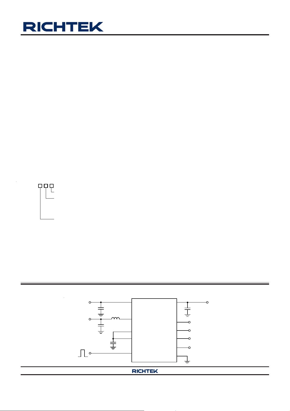
Simplified Application Circuit
Input Power
C
IN
Battery
Copyright 2014 Richtek Technology Corporation. All rights reserved. is a registered trademark of Richtek Technology Corporation.
©
L1
C1
C
VMID
VBUS
LXBST
VMID
SWIN2
BUTTON
RT9480
DS9480-04 December 2014 www.richtek.com
VBAT
USBOUT1
USBOUT2
LEDx
TORCH
GND
Battery
C
BAT
USB Port 1
USB Port 2
LED Indicator
Torch Function
1
Page 2
RT9480
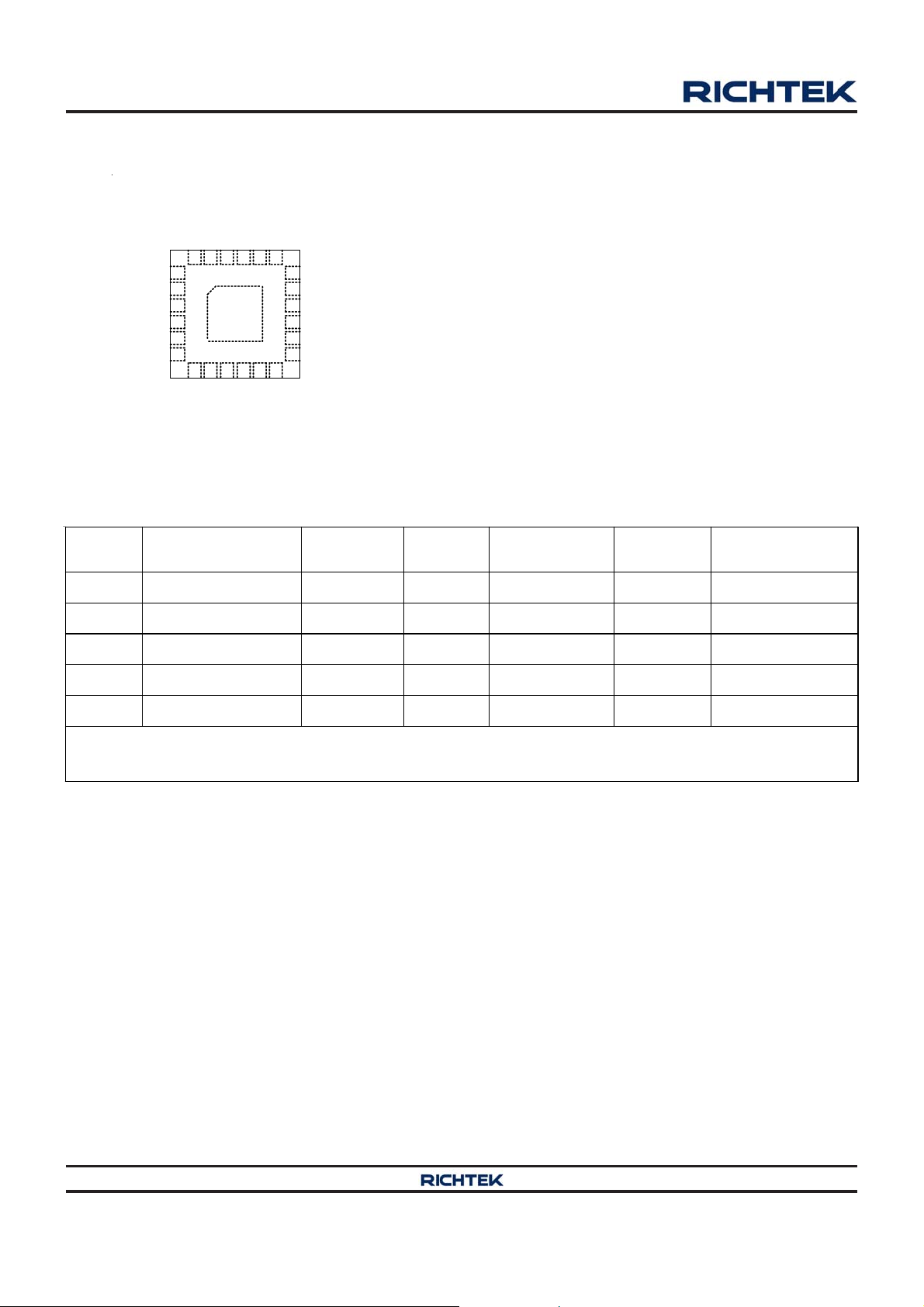
Pin Configurations
(TOP VIEW)
Marking Information
For marking information, contact our sales re presentative
directly or through a Richtek distributor located in your
area.
LXBST
VMID
LXBST
21 20 1924 2223
18
USBOUT1
17
USBOUT1
16
SWIN2
15
25
TORCH
USBOUT2
14
NC
13
TP2
TP1
BUTTON
VBAT
TS
LED1
LED2
LED3
LED4
VBUS
PGNDBST
1
2
3
4
5
6
78910 1211
NC
NC
PGNDBST
GND
GND
WQFN-24L 4x4
Product Name List
Serial
Number
Product Name Auto/Button
RT9480GQW Button 4LEDs Disable 4.2V 12 Hours
SOC LED
Number
Programmable
Battery
Regulation
USBOUT Detach
Time Out of
AA01 RT9480GQW-AA01 Auto 4LEDs Disable 4.2V 3sec
AA02 RT9480GQW-AA02 Button 4LEDs Disable 4.35V 12 Hours
AA03 RT9480GQW-AA03 Button 4LEDs Disable 4.2V 3sec
AB01 RT9480GQW-AB01 -- -- Enable -- --
* : Please refer to application note.
-- : Set by program
Copyright 2014 Richtek Technology Corporation. All rights reserved. is a registered trademark of Richtek Technology Corporation.
©
DS9480-04 December 2014www.richtek.com
2
Page 3
Functional Pin Description
Pin No. Pin Name Pin Function
1 VBAT Battery Char ge Cur r ent O utput .
2 TS Battery Temperature Sense Setting.
3 LED1 Current Si nk Output for LE D1.
4 LED2 Current Si nk Output for LE D2.
5 LED3 Current Si nk Output for LE D3.
6 LED4 Current Si nk Output for LE D4.
7, 8, 14 NC No Internal Connection.
9,
25 (Exposed Pad)
10 TORCH Current Si nk Output for Tor c h LE D Function. Open Drain Output
1 1 BUTTON Button Control Input for mode change.
12 TP1 Connected to GND.
13 TP2 Connected to GND.
15 USBOUT2 USB-2 Power Output .
GND
Ground. The exposed pad must be soldered to a large PCB and
connected to G ND for maxim um power di ssipat ion.
RT9480
16 SWIN2 USB-2 Power Input.
17, 18 USBOUT1 USB-1 Power Output .
19 VMID Boost Output.
20, 21 LXBST Boost Switch Output.
22, 23 PGNDBST Boost Power GND.
24 VBUS VBUS Power Supply.
Copyright 2014 Richtek Technology Corporation. All rights reserved. is a registered trademark of Richtek Technology Corporation.
DS9480-04 December 2014 www.richtek.com
©
3
Page 4
RT9480
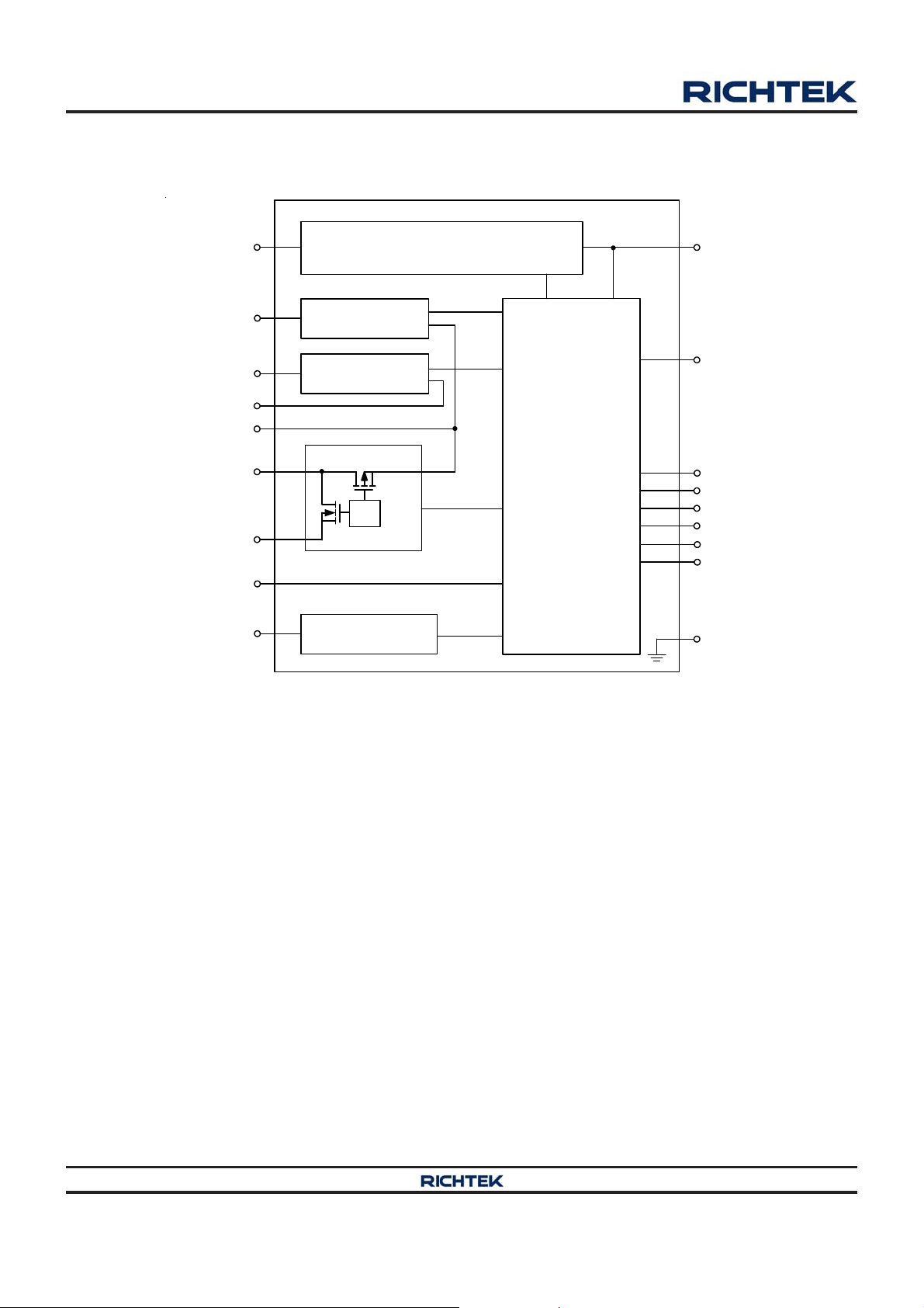
Function Block Diagram
VBUS
USBOUT1
USBOUT2
SWIN2
VMID
LXBST
PGNDBST
BUTTON
TORCH
Linear Charger 1.2A
USB-1 Load
Manager Up to 2.1A
USB-2 Load
Manager Up to 1A
Torch Brightness
Control (Open Drain)
Central Control
1. Battery Capacity
Detection
2. Protection
3. LED Display
4. Mode Control
5. Button Operation
VBAT
TS
LED1
LED2
LED3
LED4
TP1
TP2
GND
Copyright 2014 Richtek Technology Corporation. All rights reserved. is a registered trademark of Richtek Technology Corporation.
©
DS9480-04 December 2014www.richtek.com
4
Page 5

Operation
RT9480
The RT9480 is a high integrated IC for Li-Ion battery power
bank. It includes a linear charger 1.2A, a synchronous
Boost 5.1V , two output loa d ma nagement, LED indicator
and torch function.
Change Current
Ba se on thermal regulation function, the charging current
can support up to 1.2A.
VBUS OVP
If the input voltage (VBUS) is higher than the threshold
voltage V
charger will stop charging until VIN is below V
, the internal OVP signal will go high a nd the
OVP
− ΔV
OVP
OVP
VMID OVP
If the internal voltage (VMID) is higher than the threshold
voltage V
, the internal OVP signal will go high a nd the
OVP
charger will stop charging until VMID is below
V
OVP
−ΔV
OVP
.
OCP
The converter senses the current signal when the highside P-MOSFET turns on. As a result, The OCP is cycle
by-cycle current limitation. If the OCP occurs, the converter
holds off the next on pulse until inductor current drops
below the OCP limit.
OTP
The converter has a n over-temperature protection. When
the junction temperature is higher than the thermal
shutdown rising threshold, the system will be latched and
the output voltage will no longer be regulated until the
junction temperature drops under the falling threshold.
Output Short Protection
When output short to ground, the system will be latched
and the output voltage will no longer be regulated until
power reset.
.
CC/CV/TR Multi Loop Controller
There are constant current loop, consta nt voltage loop and
thermal regulation loop to control the charging current.
T oo Hot or Too Cold
The temperature sense input TS pin can be connected a
thermistor to determine whether the battery is too hot or
too cold for charging operation. If the battery's temperature
is out of range, charging is paused until it re-enters the
valid range.
Copyright 2014 Richtek Technology Corporation. All rights reserved. is a registered trademark of Richtek Technology Corporation.
DS9480-04 December 2014 www.richtek.com
©
5
Page 6
RT9480
Absolute Maximum Ratings (Note 1)
Supply Voltage, VBAT-------------------------------------------------------------------------------------- −0.3V to 6V
Supply Voltage, VBUS ------------------------------------------------------------------------------------- −0.3V to 10V
Supply V oltage USBOUT1, USBOUT2 Pulse (100μs)---------------------------------------------- −0.3V to 10V
LED Output Voltage, LED1, LED2, LED3, LED4 ---------------------------------------------------- −0.3V to 10V
TORCH--------------------------------------------------------------------------------------------------------- −0.3V to 10V
Other Pins----------------------------------------------------------------------------------------------------- −0.3V to 6V
Power Dissipation, P
WQFN-24L 4x4 ---------------------------------------------------------------------------------------------- 3.57W
Package Thermal Re sistance (Note 2)
WQFN-24L 4x4, θJA-----------------------------------------------------------------------------------------28°C/W
WQFN-24L 4x4, θJC----------------------------------------------------------------------------------------7.1°C/W
Junction T emperature Range------------------------------------------------------------------------------ 150°C
Lead T e mperature (Soldering, 10 sec.)-----------------------------------------------------------------26 0°C
Storage T emperature Range ------------------------------------------------------------------------------ −65°C to 150°C
ESD Susceptibility (Note 3)
HBM (Human Body Model)-------------------------------------------------------------------------------- 2kV
MM (Machine Model) --------------------------------------------------------------------------------------- 200V
@ TA = 25°C
D
Recommended Operating Conditions
Supply Input V oltage, VBAT, VBUS ---------------------------------------------------------------------2.8V to 5.5V
Junction T emperature Range------------------------------------------------------------------------------ −40°C to 125°C
Ambient T emperature Range------------------------------------------------------------------------------ −40°C to 85°C
(Note 4)
Electrical Characteristics
TOP Unit Electrical Characteristics
(V
= 5V, V
BUS
Supply Input
Battery Quiescent Current
for Standby
= 3.7V, T
BAT
= 25°C, unless otherwise specified)
A
Parameter Symbol Test Conditions Min Typ Max Unit
I
BAT_sdy
No VBUS, Boost
on, Indicator Off.
Button Mode -- 30 -- A
Copyright 2014 Richtek Technology Corporation. All rights reserved. is a registered trademark of Richtek Technology Corporation.
©
DS9480-04 December 2014www.richtek.com
6
Page 7

Charger Unit Electrical Characteristics
(V
BUS
= 5V, V
= 3.7V, T
BAT
= 25°C, unless otherwise specified)
A
Parameter Symbol Test Conditions Min Typ Max Unit
Supply Input
VBUS VBAT VOS Ri sing V
VBUS VBAT VOS Falling V
-- 100 200 mV
OS_H
10 50 -- mV
OS_L
Battery Charger
VBUS Operating Range V
BUS_CHG
4.5 -- 5.5 V
VBUS Regulati on DPM V
Voltage Regulation
VBAT Regulation V
Re-Charge Threshold V
VBUS Power FET R
DS(ON)
R
T
REG
V
RECHG
DS(ON)_chg IBAT
Current Regulation
Fast-Charge Current A c c ur ac y I
Pre-Charge Current Accuracy I
Pre-Charge Threshold V
Pre-Charge Threshold
Hysteresis
I
CHG
CHG_Pre
pre
V
Ratio of Fast-Char ge Cur rent 5.5 10 14.5 %
V
V
pre
Charge Termination Detection
Termination Current Ratio I
-- 10 -- %
TERMI
Timer
RT9480
= 4.5V 5 -- 5 %
DPM
= 0 to 85C, V
A
Recharge Level -- 150 -- mV
REG
= 1A -- 200 300 m
= 1.2A 5 -- 5 %
CHG
Rising 2.35 2.5 2.65 V
BAT
Falling 120 200 280 mV
BAT
= 4.2V 1 -- 1 %
REG
Fast-Charge Time Fault T
-- 24 -- hour
F_CC
Boost Unit Electrical Characteristics
(V
BUS
= 5V, V
= 3.7V, T
BAT
= 25°C, unless otherwise specified)
A
Parameter Symbol Test Conditions Min Typ Max Unit
Supply Input
Output Voltage V
Output Voltage Accuracy V
OUTBST
OUTBST
MAX Output Current As V
PFET Peak Current Limit I
OCP
-- 5.1 -- V
5 -- 5 %
BAT
> 3.3V, V
= 5V -- 2.5 -- A
OUT
6 -- -- A
Power Switch
Switching Frequency fSW 0.2 0.25 0.3 MHz
Protection
Over-Volt age Protection V
Over-Volt age Protection
Hysteresis
Under-Volt age P r otection
(Short-Circuit Protection)
MID_OVP
V
MID_O VP_hys
V
BST_FBUV
5.6 5.7 6 V
-- 0.2 -- V
-- 3.37 -- V
Copyright 2014 Richtek Technology Corporation. All rights reserved. is a registered trademark of Richtek Technology Corporation.
DS9480-04 December 2014 www.richtek.com
©
7
Page 8

RT9480
Others Electrical Characteristics
(V
BUS
LED
= 5V, V
= 3.7V, T
BAT
= 25°C, unless otherwise specified)
A
Parameter Symbol Test Conditions Min Typ Max Unit
LED Current Sink I
Torch
Open-Drain Low Voltage V
Button
Logic-High V
Button Contr ol
Logic-Low V
Press Duty
Time
High-Level T
Low-Level T
Protection
Charger Thermal Regulation T
Over-Tem per ature P r otect T
Over-Tem per ature P r otect
Hysteresis
VBUS OVP Threshold Voltage V
VBUS OVP Threshold Voltage
Hysteresis
BASE
VBUS Attached Threshold
Voltage
VBUS Attached Threshold
Voltage Hyster esi s
-- 0.75 -- mA
LED
I
ODL_T
1.5 -- -- V
IH_B
-- -- 0.4 V
IL_B
Press_H
Press_L
REG
OTP
T
OVP
V
OVP_Hys
V
BUS_ATT
V
BUS_ATT_Hys
0.1 -- -- sec
0.1 -- -- sec
For Charger -- 105 -- °C
-- 150 -- °C
-- 20 -- °C
OTP
V
V
V
V
= 5mA -- 200 -- mV
SINK
Rising 6.5 6.8 7.1 V
BUS
Falling -- 200 280 mV
BUS
Rising 3.8 4 4.2 V
BUS
Falling -- 200 280 mV
BUS
Note 1. Stresses beyond those listed “Absolute Maximum Ratings” may cause permanent damage to the device. These are
stress ratings only, and functional operation of the device at these or any other conditions beyond those indicated in
the operational sections of the specifications is not implied. Exposure to absolute maximum rating conditions may
affect device reliability.
Note 2. θ
Note 3. Devices are ESD sensitive. Handling precaution is recommended.
Note 4. The device is not guaranteed to function outside its operating conditions.
Copyright 2014 Richtek Technology Corporation. All rights reserved. is a registered trademark of Richtek Technology Corporation.
8
is measured at T
JA
©
= 25°C on a high effective thermal conductivity four-layer test board per JEDEC 51-7.
A
DS9480-04 December 2014www.richtek.com
Page 9

Typical Application Circuit
IN
VMID
100k
100k
24
16
19
20, 21
22, 23
11
12
13
VBUS
SWIN2
VMID
LXBST
PGNDBST
BUTTON
TP1
TP2
Input Power
V
BAT
V
BAT
1µH
C1
10µF
Button
C
1µF/25V
C
22µF x2
L1
R2
R3
RT9480
USBOUT1
USBOUT2
VBAT
TS
LED1
LED2
LED3
LED4
TORCH
1
2
17, 18
15
3
4
5
6
10
R1
C
BAT
10µF
C
OUT1
1µF
C
OUT2
1µF
D1
D2
D3
D4
D6
USB1
Output
USB2
Output
V
BAT
Display
VMID
Power
Li-Bat
Prot-IC
RT9480
+
-
R
NTC
10k
Semitec
103AT
N-MOSFET
9, 25 (Exposed Pad)
GND
Copyright 2014 Richtek Technology Corporation. All rights reserved. is a registered trademark of Richtek Technology Corporation.
©
DS9480-04 December 2014 www.richtek.com
9
Page 10

RT9480
)
Typical Operating Characteristics
USBOUT Efficiency vs. Load Current
100
90
80
70
60
50
40
Eff iciency (%)
30
20
10
0
0 500 1000 1500 2000 2500
USBOUT = 5.1V, L = 1μH, C
V
BAT
V
BAT
V
BAT
Load Current (mA)
USBOUT V ol tage vs. Temperature
5.5
5.4
5.3
5.2
5.1
5.0
4.9
4.8
Output Voltage (V)
4.7
4.6
4.5
-50 -25 0 25 50 75 100 125
V
= 3.3V
BAT
V
= 3.7V
BAT
V
= 3.9V
BAT
Temperature (°C)
USBOUT = 5.1V
= 3.9V
= 3.7V
= 3.3V
= 1μF
OUT
USBOUT Voltage vs. Load Current
6.0
5.5
5.0
V
= 3.3V
BAT
V
= 3.7V
4.5
4.0
BAT
= 3.9V
V
BAT
Output Voltage (V)
3.5
3.0
0 500 1000 1500 2000 2500
USBOUT = 5.1V
Load Current (mA)
VBUS OVP Threshold Voltage vs. Tempe rature
7.2
7.0
6.8
6.6
6.4
6.2
OVP Threshol d Voltage (V)
6.0
-50 -25 0 25 50 75 100 125
Rising
Falling
VBAT = Real Battery
Tempera ture (°C)
Battery Regulation Voltage vs. Temperature
4.25
4.22
105°C
4.19
4.16
4.13
Battery Regulation V oltage (V) 1
Copyright 2014 Richtek Technology Corporation. All rights reserved. is a registered trademark of Richtek Technology Corporation.
VIN = 5V , VB AT = Real Battery
4.10
-50 -25 0 25 50 75 100 125
Temperatur e (°C)
©
ICHG Thermal Regulation vs. Temperature
1300
1200
1100
1000
900
800
700
600
500
400
300
200
ICHG Thermal Regulat ion (mA
100
VIN = 5V , VB AT = Real Battery
0
-50 -25 0 25 50 75 100 125
Temperatur e (°C)
DS9480-04 December 2014www.richtek.com
10
Page 11

Application Information
RT9480
The RT9480 is a high integrated IC for Li-Ion battery power
bank. This chi p includes a linear charger , a synchronous
Boost, two output load management, LED indicator and
torch function.
Pre-Charge Mode
When the output voltage is lower than 2.3V, the charging
current will be reduced to a fast-charge current ratio to
protect the battery life time.
Fast-Charge Mode
When the output voltage is higher than 2.5V, the charging
current will be equal to the fast-charge current with 1.2A.
Constant-Voltage Mode
When the output voltage is near 4.2V or 4.35V , the charging
current will fall below the termination current.
Re-Charge Mode
When the chip is in charge termination mode, the charging
current will gradually go down to zero. However, once the
voltage of the battery drops to below 4.05V or 4.2V, then
the charging current will resume again.
battery in order to maintain thermal regulation at around
105°C. This operation continues until the junction
temperature falls below the thermal regulation threshold
(105°C) by the hysteresis level. This feature prevents the
maximum power dissipation from exceeding typical design
conditions.
Time Fault
The Fast-Charge Fault T i me is set by 24hours.
When time fault ha ppens, the charger cycle will be turned
off charging function.
Battery Pack Temperature Monitoring
The RT9480 features an extern al battery pack temperature
monitoring input. The TS input connects to the NTC
thermistor in the battery pack to monitor battery
temperature and prevent danger over temperature
conditions. If at any ti me the voltage at TS falls outside of
the operating range, charging will be suspended. The NTC
thermistor recommends using 10kΩ.
JEIT A Function
For JEIT A battery temperature sta ndard :
Charge Termination
When the charge current is lower than the charge
termination current ratio (10%) for V
> 4.05V or 4.2V
BAT
and the time is larger tha n the deglitch time (25ms), it will
be latched high unless the power is re-toggled.
Input DPM Mode
If the input voltage is lower than V
(4.5V), the input
DPM
current limit will be reduced to stop the input voltage from
dropping any further . This can prevent the IC from da maging
improperly configured or inadequately designed USB
sources.
Temperature Regulation
In order to maximize charge rate, the RT9480 features a
junction temperature regulation loop. If the power
dissipation of the IC results in junction temperature greater
than the thermal regulation threshold (105°C), the R T9480
will cut back on the charge current a nd disconnect the
CV regulation voltage will change at the f ollowing battery
T emp ra nges 45°C to 60°C.
4.35V or 4.2V
4.2V or 4.05V
100% Ichg
50% Ichg
010 4560
C C
C C
Synchronous Step-Up
The converter operates in fixed frequency PWM Mode
with 250kHz, Continuous Current Mode (CCM), and
Discontinuous Current Mode (DCM) with internal
MOSFETs.
Copyright 2014 Richtek Technology Corporation. All rights reserved. is a registered trademark of Richtek Technology Corporation.
DS9480-04 December 2014 www.richtek.com
©
11
Page 12

RT9480
Operation Method
Charge Mode : VBUS in and charging battery
Discharge Mode : USBOUT in and discharging for ha ndheld
Chg-Dchg Mode : VBUS and USBOUT in, charging battery
and discharging ha ndheld at the sa me tim e
Button Mode
Button mode : When external handheld device plug in f or
power bank, the USBOUT will turns on by button.
If device attched, RT9480 will count 12 hours
(RT9480GQW or AA02) or 3sec (AA01 or AA03) to turn
off USBOUT after deta ch.
Relax Mode : VBUS and USBOUT plug out
AA01 and AA03. Plea se reference Product N a me List.
Attach mea n device plug in a nd loading > 100mA.
Detach mea n device plug out and loa ding < 50mA.
Button Function
Function Button Action Description
After plugging in t he exter nal power sour c e, the power
Micro-USB Adapter
plug-in : ON
Charging NA
Micro-USB Adapter
plug-out : OFF
bank will be charged aut omatically without pressing the
button, and the LE D batt er y indicator lights up at the
same time.
After unplugging t he exter n al power source, the power
bank stops being charged automatically wit h out pressing
the button, and t he LED battery indicat or fades out at the
same time.
After plugging in t he H/H dev ic e and pr essing the button,
the power bank starts to charge the device.
After unplugging the H/H device, the power bank stops
charging the dev ic e automatically without pressing the
Discharging
0.1s
USB slave plug-in : ON
USB slave plug-out : OF F
button.
Check Battery
Capacity
Torch
0.1s
0.1s 0.1s
Press the button (short
press) one time : ON
After 20sec : OFF After 20sec, the LED batt er y indicator fades out.
Double clic k the butt o n
(short press) : ON
Double clic k the butt o n
(short press : OFF
Press the button (short pres s), the LED battery indicator
lights up.
Double click the button (short press), the torch light li ghts
up.
Double click the button (short press) again, the torch light
fades out.
Copyright 2014 Richtek Technology Corporation. All rights reserved. is a registered trademark of Richtek Technology Corporation.
12
©
DS9480-04 December 2014www.richtek.com
Page 13

RT9480
BUTTON Press Timing
Define Button (Short/Long) Press Timing
Short press = min (0.1s)
Blank = min (0.1s)
SOC LED Flash and Running Timing
SOC LED Fla sh
0.5s
0.5s
SOC LED Running
LED Indicator Function
About LED indicator, it will follow below table to show
SOC. The LED current is 0.75mA.
●●●●
Low→High
● : LED ON, ○ : LED OFF, ● : LED FLASH
Battery Voltage Operation of Charging
●○○○
3700mV
●●○○
●●●○
●●●●
●●○○
3700mV
3940mV
●●●○
●●●●
0.5s
0.5s
0.5s
3940mV
4100mV
●●●○
●●●●
4100mV
4200mV
●●●●
4200mV ●●●●
Battery Vol t age Operation of Discharging
4200mV
3880mV
3880mV
3720mV
3720mV
3500mV
3500mV
3200mV
3200mV
2800mV
●●●●
●●●○
●●○○
●○○○
●○○○
Copyright 2014 Richtek Technology Corporation. All rights reserved. is a registered trademark of Richtek Technology Corporation.
DS9480-04 December 2014 www.richtek.com
©
13
Page 14

RT9480
Thermal Considerations
For continuous operation, do not exceed absolute
maximum junction temperature. The maximum power
dissipation depends on the thermal resistance of the IC
package, PCB layout, rate of surrounding airflow, and
difference between junction and a mbient temperature. The
maximum power dissipation can be calculated by the
following formula :
P
where T
the ambient temperature, a nd θ
D(MAX)
= (T
J(MAX)
− TA) / θ
J(MAX)
JA
is the maximum junction temperature, TA is
is the junction to ambient
JA
thermal resistance.
For recommended operating condition specifications, the
maximum junction temperature is 125°C. The junction to
a mbient thermal resistance, θJA, is layout dependent. For
WQFN-24L 4x4 package, the thermal resistance, θJA, is
28°C/W on a standard JEDEC 51-7 f our-layer thermal test
board. The maximum power dissipation at TA = 25°C can
be calculated by the following formula :
Layout Consideration
The PCB layout is an importa nt step to maintain the high
performance of the R T9480.
Both the high current and the fa st switching nodes demand
full attention to the PCB layout to save the robustness of
the RT9480 through the PCB layout. Improper layout might
show the symptoms of poor line or load regulation, ground
and output voltage shifts, stability issues, unsatisfying
EMI behavior or worsened efficiency.For the best
performance of the RT9480, the following PCB layout
guidelines must be strictly followed.
Place the input and output capacitors as close as
possible to the input and output pins respectively for
good filtering.
Care should be taken for a proper thermal layout. Wide
traces, connecting with vi as through the layers, provides
a proper thermal path to sink the heat energy created
from the device and inductor . Keep the main power traces
as wide a nd short as possible. Recommend as below :
P
= (125°C − 25°C) / (28°C/W) = 3.57W for
D(MAX)
WQF N-24L 4x4 pa ckage
The maximum power dissipation depends on the operating
ambient temperature for fixed T
and thermal
J(MAX)
resistance, θJA. The derating curve in Figure 1 allows the
designer to see the effect of rising ambient temperature
on the maximum power dissipation.
4.0
3.5
3.0
2.5
2.0
1.5
1.0
0.5
Maximum Power Dissipati on ( W ) 1
0.0
0 25 50 75 100 125
Ambient Temperature (°C)
Four-Layer PCB
VBUS trace > 40mil;
VBAT trace > 80mil;
LXBST trace > 80mil;
VMID tra ce > 40mil;
USBOUT1 trace > 80mil;
USBOUT2 trace > 40mil.
The switching node area connected to LX and inductor
should be minimized for lower EMI.
Connect the GND pin, PGNDBST pin a nd Exposed Pad
together to a strong ground plane for maxi mum thermal
dissipation and noise protection.
Directly connect the output cap acitors to the feedback
network of each cha nnel to avoid bouncing caused by
parasitic resista nce and inducta nce from the PCB trace.
Figure 1. Derating Curve of Maxi mum Power Dissi pation
Copyright 2014 Richtek Technology Corporation. All rights reserved. is a registered trademark of Richtek Technology Corporation.
14
©
DS9480-04 December 2014www.richtek.com
Page 15

Input capacitors
must be placed
as close as
possible to the
Input pins.
GND
VBAT
GND
RT9480
LX should be connected to Inductor by
wide and short trace, keep sensitive
compontents away from this trace
L1
LXBST
LXBST
10 11 12
TORCH
BUTTON
R1
D6
VMID
VMID
19202124
TP1
C
18
17
16
15
14
13
R2
MID
USBOUT1
USBOUT1
SWIN2
USBOUT2
NC
TP2
VMID
R3
C
OUT1
GND
USBOUT1
VMID
USBOUT2
C
OUT2
GND
Output
capacitors must
be placed as
close as
possible to the
Output pins.
Connect GND
Pin and PGND
Pin to Exposed
Pad.
VBAT
C
BAT
R
NTC
D1
D2
D3
D4
VBAT
LED1
LED2
LED3
LED4
VBUS
C
VBUS
1
2
TS
3
4
5
6
78
NC
C1
GND
IN
PGNDBST
PGNDBST
2223
GND
9
NC
GND
Connect the Exposed Pad to a ground
plane.
Figure 2. PCB Layout Guide
Copyright 2014 Richtek Technology Corporation. All rights reserved. is a registered trademark of Richtek Technology Corporation.
©
DS9480-04 December 2014 www.richtek.com
15
Page 16

RT9480
Outline Dimension
D
D2
SEE DETAIL A
L
1
E
be
A
A3
A1
E2
1
2
1
2
DETAIL A
Pin #1 ID a nd T ie Bar Mark Option s
Note : The configuration of the Pin #1 identifier is optional,
but must be located within the zone indicated.
Dimensions In Millimeters Dimensions In Inches
Symbol
Min Max Min Max
A 0.700 0.800 0.028 0.031
A1 0.000 0.050 0.000 0.002
A3 0.175 0.250 0.007 0.010
b 0.180 0.300 0.007 0.012
D 3.950 4.050 0.156 0.159
Option 1 2.400 2.500 0.094 0.098
D2
Option 2 2.650 2.750 0.104 0.108
E 3.950 4.050 0.156 0.159
Option 1 2.400 2.500 0.094 0.098
E2
Option 2 2.650 2.750 0.104 0.108
e 0.500 0.020
L 0.350 0.450 0.014 0.018
W-Type 24L QFN 4x4 Package
Richtek Technology Corporation
14F, No. 8, Tai Yuen 1st Street, Chupei City
Hsinchu, Taiwan, R.O.C.
Tel: (8863)5526789
Richtek products are sold by description only. Richtek reserves the right to change the circuitry and/or specifications without notice at any time. Customers should
obtain the latest relevant information and data sheets before placing orders and should verify that such information is current and complete. Richtek cannot
assume responsibility for use of any circuitry other than circuitry entirely embodied in a Richtek product. Information furnished by Richtek is believed to be
accurate and reliable. However, no responsibility is assumed by Richtek or its subsidiaries for its use; nor for any infringements of patents or other rights of third
parties which may result from its use. No license is granted by implication or otherwise under any patent or patent rights of Richtek or its subsidiaries.
DS9480-04 December 2014www.richtek.com
16
Page 17

 Loading...