

RT9396
I2C Interface PMIC with 6-Channel WLED Driver and 4-LDO
General Description
The RT9396 is a power management IC (PMIC) for
backlighting and phone camera applications. The PMIC
contains a 6-Channel charge pump white LED driver and
four low dropout linear regulators.
The charge pump drives up to 6 white LEDs with regulated
constant current for uniform intensity. Each channel
(LED1 to LED6) supports up to 25mA of current. These
6-Channels can be also programmed as 4 plus 2-Channels
or 5 plus 1-Channel with different current setting for
auxiliary LED application. The RT9396 maintains highest
efficiency by utilizing a x1/ x1.5/ x2 fractional charge pump
and low dropout current regulators. An internal 6-bit DAC
is used for backlight brightness control. Users can easily
configure up to 64 steps of LED current via the I2C interface
control.
The RT9396 also comprises low noise, low dropout
regulators, which provide up to 200mA of current for each
of the four channels. The four LDOs deliver 3% output
accuracy and low dropout voltage of 200mV @ 200mA.
Users can easily configure LDO output voltage via the I2C
interface control. The LDOs also provide current limiting
and over temperature functions.
Features
zz
Tri-Mode (x1/x1.5/x2) Charge Pump
z
zz
zz
z Maximum 25mA x 6-Channel LED Backlighting
zz
Output Current
zz
z Support Main/Sub (4+2/5+1) LED Function
zz
zz
z 64 Steps Programmable LED Current
zz
zz
z Support PWM Dimming Function
zz
zz
z Fade In/Out Via I
zz
zz
z 4 Low Dropout Regulators
zz
zz
z Maximum 200mA x 4-Channel LDO Output Current
zz
zz
z 16-Level LDO Output V oltage Setting
zz
2
zz
z I
C Programmable Independent LDO Channel
zz
2
C Control
ON/OFF Control
zz
z Over Temperature Protection
zz
zz
z Thin 24-Lead WQFN Package
zz
zz
z RoHS Compliant and Halogen Free
zz
Applications
z Cellular Phones
z PDAs and Smart Phones
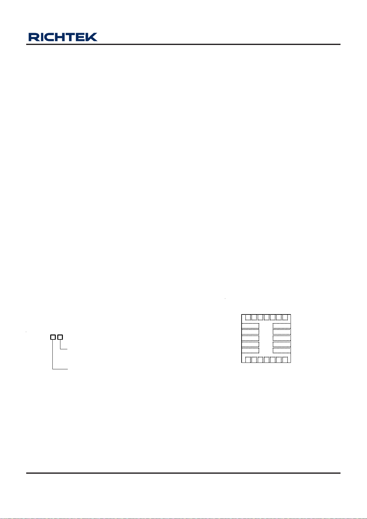
Pin Configurations
(TOP VIEW)
The RT9396 is available in a WQFN-24L 3x3 package.
Ordering Information
RT9396
Package Type
QW : WQFN-24L 3x3 (COL) (W-Type)
Lead Plating System
G : Green (Halogen Free and Pb Free)
Note :
VOUT
PGND
C2N
C1N
C1P
C2P
1
2
3
4
5
6789 1110
AGND
WQFN-24L 3x3 (COL)
LED1
VIN
LED2
LDOIN
LED3
LED5
LED4
21 20 1924 2223
18
17
SCL
16
SDA
15
EN
14
PWM
13
CF
12
LDO1 LED6
LDO2
LDO3
LDO4
Richtek products are :
RoHS compliant and compatible with the current require-
ments of IPC/JEDEC J-STD-020.
Suitable for use in SnPb or Pb-free soldering processes.
DS9396-01 April 2011 www.richtek.com
1
RT9396
Marking Information
JP= : Product Code
JP=YM
DNN
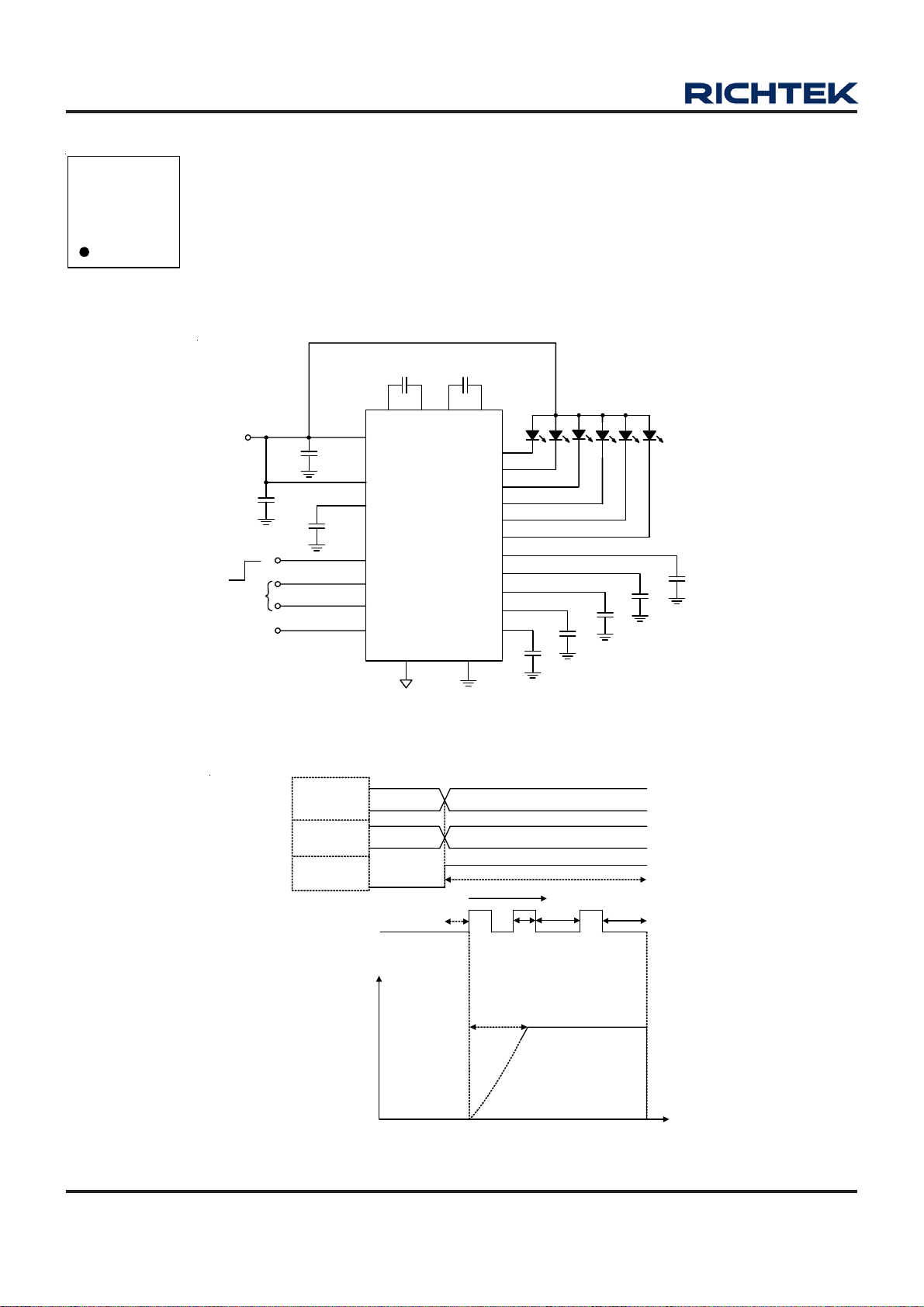
Typical Application Circuit
YMDNN : Date Code
V
Chip Enable
Timing Diagram
Note:
PWM signal rise after
internal PWMEN is
enabled
BAT
I2C
PWM
2
C
I
Reg. Addr.
2
I
C
Reg. Data
C
IN2
2.2µF
LED<1:6>
Current Level
PWMEN Reg.
Main I
C
IN1
2.2µF
C
F
1µF
010
On/Off
Main BL
Internal
PWM Pin
LED
C1P C1N C2P
7
VIN
8
LDOIN
1
3
CF
1
5
EN
1
7
SCL
1
6
SDA
1
4
PWM
00000000
00000000
[1:6]
C
FLY1
1µF
4
AGND
6
C
FLY2
1µF
3
5
2
C2N
2
3
LED1
2
2
RT9396
LED2
2
1
LED3
2
0
LED4
1
9
LED5
1
8
LED6
2
4
VOUT
1
2
LDO1
1
1
LDO2
1
0
LDO3
9
LDO4
PGND
1
01011111
6CH PWM Mode
01111101
Fade in/out time = 8ms/step, I
PWM control Backlight
THi > 0.5µs
Fade in
time
C
L2
1µF
C
L3
C
1µF
L4
1µF
[1~6] = 62/64 x 25mA
LED
PWM Dimming
0.5µs < T
I
[1~6] Current =
LED
62/64 x 25mA x PWM Duty
LO
T
< 500µs
SHD
C
L1
1µF
= 16m s
WLED
C
1µF
OUT
0
Time (s)
Figure 1. Timing Diagram
DS9396-01 April 2011www.richtek.com
2
RT9396
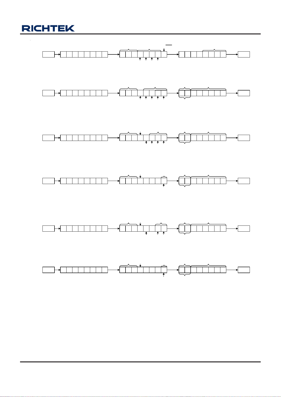
2
• I
C Writing Cycles of LDOX
2
• I
C Writing Cycles of Backlighting I (LED1~6)
1 0 1 0 1 0 0 0
2
• I
C Writing Cycles of Backlighting II (Main: LED1~5, Sub: LED6)
1 0 1 0 1 0 0 0
1 0 1 0 1 0 0 0
LDO
Address
0 0 1 B4 B3 B2 B1 B0 0 0 0 0 C3 C2 C1 C0Start Stop1 0 1 0 1 0 0 0
Backlight
Address
Backlight
Address
Backlight
Address
LDO4
PWMEN
Main
Sub
Channel
Selection
LDO3
Channel
ON/OFF
LED6
Channel
ON/OFF
PWMENPWMEN
LDO2
LED5
LED5
ON/OFF
LDO1
LED4
LED1~3
LED4
LED1~3
Channel
ON/OFF
16-step Voltage
Setting
Fade In/Out
Setting
C7 C6 C5 C4 C3 C2 C1 C00 x x x x x0 1 0 B4 B3 B2 B1 B0
Fade In/Out Setting:
01: Every Step of Fade In/Out = 8 ms
BLON
10: Every Step of Fade In/Out = 16 ms
11: Every Step of Fade In/Out = 32 ms
Fade In/Out
Setting
C7 C6 C5 C4 C3 C2 C1 C00 x x x x x0 1 1 0 B3 B2 B1 B0
Main Fade In/Out Setting:
01: Every Step of Fade In/Out = 8 ms
10: Every Step of Fade In/Out = 16 ms
Main ON
11: Every Step of Fade In/Out = 32 ms
Fade In/Out
Setting
C7 C6 C5 C4 C3 C2 C1 C00 x x x x x0 1 1 1 0 0 0 B0
64-step Current Setting
Main 64-step Current Setting
Sub 64-step Current Setting
StopStart
StopStart
StopStart
2
• I
C Writing Cycles of Backlighting III (Main: LED1~4, Sub: LED5~6)
1 0 1 0 1 0 0 0
1 0 1 0 1 0 0 0
Figure 2. Control Sequences of LDO Setting and LED Dimming
Backlight
Address
Backlight
Address
Main
Sub
Channel
ON/OFF
LED4
Channel
ON/OFF
Sub Fade In/Out Setting:
LED6
LED1~3
LED5~6
01: Every Step of Fade In/Out = 8 ms
10: Every Step of Fade In/Out = 16 ms
Sub ON
11: Every Step of Fade In/Out = 32 ms
Fade In/Out
Setting
C7 C6 C5 C4 C3 C2 C1 C00 x x x x x1 0 0 0 B2 0 B1 B0
Main Fade In/Out Setting:
01: Every Step of Fade In/Out = 8 ms
10: Every Step of Fade In/Out = 16 ms
Main ON
11: Every Step of Fade In/Out = 32 ms
Fade In/Out
Setting
C7 C6 C5 C4 C3 C2 C1 C00 x x x x x1 0 0 1 0 0 0 B0
Sub Fade In/Out Setting:
01: Every Step of Fade In/Out = 8 ms
10: Every Step of Fade In/Out = 16 ms
Sub ON
11: Every Step of Fade In/Out = 32 ms
Main 64-step Current Setting
StopStart
Sub 64-step Current Setting
StopStart
DS9396-01 April 2011 www.richtek.com
3

RT9396
Functional Pin Description
Pin No. Pin Name Pin Function
1 PGND Charge Pump Ground.
2 C2N Fly Capa ci tor 2 Negative Conne cti on.
3 C1N Fly Capa ci tor 1 Negative Conne cti on.
4 C1P Fly Capacitor 1 Positi ve Connection.
5 C2P Fly Capacitor 2 Positi ve Connection.
6 AGND Ground for LDO1 to LDO4.
7 VIN Charge Pump Power I npu t. Con nect th is pi n to LDOIN pin.
8 LDOIN LDO Power Input. Connect this pin to VIN pin.
9 LDO4 LDO4 Out put.
10 LDO3 LDO3 Out put.
11 LDO2 LDO2 Output.
12 LDO1 LDO1 Out put.
13 CF PWM Fi lter Ca paci tor Connection.
14 PWM PWM Dimming Control Input.
15 EN Chip Enable (Active High).
16 SDA I2C Data Input.
17 SCL I2C Clock Input.
18 LED6 Current Sink for LED6.
19 LED5 Current Sink for LED5.
20 LED4 Current Sink for LED4.
21 LED3 Current Sink for LED3.
22 LED2 Current Sink for LED2.
23 LED1 Current Sink for LED1.
24 VOUT Charge Pump Output. Connect a 1μF ceramic capacitor be tween VOUT and GND.
DS9396-01 April 2011www.richtek.com
4
Function Block Diagram
RT9396
VIN
CF
PWM
SDA
SCL
1MHz
Oscillator
Mode
Decision
PWM
Dimming
Shutdown
Delay
LED
Ctrl.
I2C
C1P
C1N
x1/x1.5/x2
Charge Pump
Gate Driver
Current Setting
OR
Gate
LDO
Ctrl.
C2P
C2N
OVP
Soft Start
Current Source
OTP &
Current Bias
V
VOUT
LED1
LED2
LED3
LED4
LED5
LED6
OUT
EN
AGND
PGND
POR
Table 1. 16-Step LDO Output Voltage Setting
C3 C2 C1 C0
LDO1 &
LDO2 Ou tp ut
Voltag e (V)
LDO3 & LDO4
Output
Volt age (V)
0 0 0 0 1 1.1
0 0 0 1 1.1 1.2
0 0 1 0 1.2 1.4
0 0 1 1 1.3 1.7
0 1 0 0 1.5 1.8
BandGap
Reference
LDOIN
+
RES Divider
Voltage Setting
x4
C3 C2 C1 C0
LDOIN
LDO1 to
LDO4
LDO1 &
LDO2 Output
Vol ta ge (V)
LDO3 & LDO4
Output
Voltage (V)
1 0 0 0 2.5 2.2
1 0 0 1 2.6 2.3
1 0 1 0 2.7 2.4
1 0 1 1 2.8 2.5
1 1 0 0 2.9 2.8
0 1 0 1 1.6 1.9
0 1 1 0 1.8 2
0 1 1 1 2.1 2.1
DS9396-01 April 2011 www.richtek.com
1 1 0 1 3 2.85
1 1 1 0 3.1 3.2
1 1 1 1 3.3 3.3
5
RT9396
Table 2. 64-Step WLED Current Setting
C5 C4 C3 C2 C1 C0
0 0 0 0 0 0 0.39
0 0 0 0 0 1 0.78
0 0 0 0 1 0 1.17
0 0 0 0 1 1 1.56
0 0 0 1 0 0 1.95
0 0 0 1 0 1 2.34
0 0 0 1 1 0 2.73
0 0 0 1 1 1 3.13
0 0 1 0 0 0 3.52
0 0 1 0 0 1 3.91
0 0 1 0 1 0 4 .3
0 0 1 0 1 1 4.69
0 0 1 1 0 0 5.08
0 0 1 1 0 1 5.47
0 0 1 1 1 0 5.86
0 0 1 1 1 1 6.25
0 1 0 0 0 0 6.64
0 1 0 0 0 1 7.03
0 1 0 0 1 0 7.42
0 1 0 0 1 1 7.81
0 1 0 1 0 0 8 .2
0 1 0 1 0 1 8.59
0 1 0 1 1 0 8.98
0 1 0 1 1 1 9.38
0 1 1 0 0 0 9.77
0 1 1 0 0 1 10 .16
0 1 1 0 1 0 10 .55
0 1 1 0 1 1 10 .94
0 1 1 1 0 0 11 .33
0 1 1 1 0 1 11 .72
0 1 1 1 1 0 12 .11
0 1 1 1 1 1 12.5
WLED
Current (mA)
C5 C4 C3 C2 C1 C0
1 0 0 0 0 0 12 .89
1 0 0 0 0 1 13 .28
1 0 0 0 1 1 14 .06
1 0 0 1 0 0 14 .45
1 0 0 1 0 1 14 .84
1 0 0 1 1 0 15 .23
1 0 0 1 1 1 15 .63
1 0 1 0 0 0 16 .02
1 0 1 0 0 1 16 .41
1 0 1 0 1 0 16.8
1 0 1 0 1 1 17 .19
1 0 1 1 0 0 17 .58
1 0 1 1 0 1 17 .97
1 0 1 1 1 0 18 .36
1 0 1 1 1 1 18 .75
1 1 0 0 0 0 19 .14
1 1 0 0 0 1 19 .53
1 1 0 0 1 0 19 .92
1 1 0 0 1 1 20 .31
1 1 0 1 0 0 20.7
1 1 0 1 0 1 21 .09
1 1 0 1 1 0 21 .48
1 1 0 1 1 1 21 .88
1 1 1 0 0 0 22 .27
1 1 1 0 0 1 22 .66
1 1 1 0 1 0 23 .05
1 1 1 0 1 1 23 .44
1 1 1 1 0 0 23 .83
1 1 1 1 0 1 24 .22
1 1 1 1 1 0 24 .61
1 1 1 1 1 1 25
WLED
Current (mA)
6
DS9396-01 April 2011www.richtek.com

Absolute Maximum Ratings (Note 1)
RT9396
z Supply Input Voltage, V
z Output Voltage, V
z Other Pins ----------------------------------------------------------------------------------------------------------------- −0.3V to 6V
z Power Dissipation, P
OUT
---------------------------------------------------------------------------------------------- −0.3V to 6V
IN
-----------------------------------------------------------------------------------------------------------------------------------------------
@ T
D
= 25°C
A
−6V to 0.3V
WQFN-24L 3x3 ----------------------------------------------------------------------------------------------------------- 1.667W
z Package Thermal Resistance (Note 2)
WQFN-24L 3x3, θJA----------------------------------------------------------------------------------------------------- 60°C/W
z Junction Temperature --------------------------------------------------------------------------------------------------- 150°C
z Lead Temperature (Soldering, 10 sec.) ----------------------------------------------------------------------------- 260°C
z Storage Temperature Range ------------------------------------------------------------------------------------------- −65°C to 150°C
z ESD Susceptibility (Note 3)
HBM (Human Body Mode) --------------------------------------------------------------------------------------------- 2kV
MM (Machine Mode) ---------------------------------------------------------------------------------------------------- 200V
Recommended Operating Conditions
z Supply Input Voltage, V
z Junction Temperature Range ------------------------------------------------------------------------------------------ −40°C to 125°C
z Ambient Temperature Range ------------------------------------------------------------------------------------------ −40°C to 85°C
, V
IN
------------------------------------------------------------------------------------ 2.8V to 5V
LDOIN
(Note 4)
Electrical Characteristics
(V
= V
IN
specification)
Input Power Supply
Under -Voltage Lock out Threshold V
Under -Voltage Lockout Hysteresis ΔV
Quies cent of x1 Mode I
Quies cent of x2 Mode I
Shutdown Current I
Charge Pump WLED Driver
Backlight I
Backlight Current Matching −3 0 3 %
Dropou t Voltage -- 70 -- mV
Charge Pump
Oscilla tor F requency -- 100 0 -- kHz
LDOIN
= 3.6V, C
= 2.2μF, C
IN
= 1μF, C
OUT
FLY1
= C
= 1μF, VF = 3.5V, I
FLY2
= 25mA, TA = 25°C, unless otherwise
LEDx
Parameter Symbol Test Conditions Min Typ Max Unit
VIN Rising. 1.8 2.1 2.5 V
UVLO
-- 200 -- mV
UVLO
Q_x1
Q_x2
SHDN
Accuracy −5 0 5 %
LEDx
LDO[1:4] OFF
x2 Mode, V
LDO[1:4] OFF
VIN = 5V, VEN = 0V -- 0.5 1 μA
x1 Mode, V
= 5V, No Load,
IN
= 3.5V, No Load,
IN
-- 1 2 mA
-- 3.5 5 mA
x1 Mode to x1.5 Mode
Transition Voltage (V
falling)
IN
Mode Transiti on Hysteresis Vf = 3.5V, I
Over Voltag e Protecti on V
V
= 3.5V, I
f
= 4.5V 5.2 5.5 5.8 V
IN
= 150mA -- 3.6 3.75 V
OUT
= 150mA -- 250 -- mV
OUT
T o be continued
DS9396-01 April 2011 www.richtek.com
7

RT9396
Parameter Symbol Test Conditions Min Typ Max Unit
LDO1 to L DO4
Input Voltag e VIN = 2.8V to 5V 2.8 -- 5 V
Dropou t Voltag e VIN ≥ 2.8 V, I
Ou tput voltage Range By I2C Sett ing 1.1 -- 3. 3 V
VOUT Accuracy I
Line Regulation
Load Regulation 1mA < I
Current Limit I
R
LIM
= 1mA −3 3 %
OUT
= (V
V
IN
OUT
> 2.5V, whichever is larg er
V
IN
OUT
= 1Ω 230 350 600 mA
LOAD
Qu ies cent Current IQ 4-Chan nel All Turn O n -- 140 200 μA
Shutdown Current I
-- -- 1 μA
SHDN
Thermal Shutdown TSD -- 160 -- °C
Thermal Shutdown Hysteresis ΔTSD -- 20 -- °C
I2C interface
EN, SDA,SCL Pull Low Current IEN -- 5 10 μA
EN, SDA, SCL
Threshold Voltage
Logic-High VIH 1.4 -- -- V
Logic-Low V
-- -- 0.4 V
IL
SDA Output Low Voltage VCL -- -- 0.4 V
SCL Clock Frequ enc y f
SCL Clock Low Period t
SCL Clock High Period t
Hold Time START Co ndition t
Setup Time fo r Repe at START t
SDA Data Setup Time t
SDA Data HOLD Time t
Setup Time fo r STOP Condition t
Bus Free Time Between STOP and
START Condition
-- -- 400 kHz
SCL
1.3 -- -- μs
Low
0.6 -- -- μs
High
HD_STR
SU_STR
SU_DAT
HD_DAT
SU_STO
t
BUF
0.6 -- -- μs
0.6 -- -- μs
100 -- -- ns
0.05 -- 0.9 μs
0.6 -- -- μs
1.3 -- -- μs
PWM Dimming Control
PW M Dimmin g Frequency 1 -- 200 kHz
= 200 mA -- -- 200 mV
OUT
+ 0.3V) to 5V or
-- -- 0.2 %/V
< 200mA -- -- 0.6 %
PWM Dimming High Time 0.5 -- -- μs
PW M Dimmin g Lo w Time 0.5 -- 500 μs
Shutdown Delay 16 -- -- ms
Note 1. Stresses listed as the above “Absolute Maximum Ratings” may cause permanent damage to the device. These are for
stress ratings. Functional operation of the device at these or any other conditions beyond those indicated in the
operational sections of the specifications is not implied. Exposure to absolute maximum rating conditions for extended
periods may remain possibility to affect device reliability.
Note 2. θ
Note 3. Devices are ESD sensitive. Handling precaution is recommended.
Note 4. The device is not guaranteed to function outside its operating conditions.
8
is measured in the natural convection at TA = 25°C on a high effective thermal conductivity four-layer test board of
JA
JEDEC 51-7 thermal measurement standard.
DS9396-01 April 2011www.richtek.com

)
Typical Operating Characteristics
For Charge Pump
Efficiency vs. Input Voltage
100
90
80
70
60
50
40
Efficiency (%)
30
20
10
0
2.5 3 3.5 4 4.5 5 5.5
Input Voltage (V)
Vf = 3.5V, I
LEDx
= 25mA
RT9396
LED Current vs . Input Voltage
30
29
28
27
26
25
24
23
22
21
20
LED Current (mA)
19
18
17
16
15
2.533.544.555.5
LED1
LED2
LED3
LED4
LED5
LED6
Vf = 3.5V
Input Voltage (V)
x1 Mode Quiescent Current vs. Input Voltage
3.0
2.5
2.0
1.5
1.0
Quiesent Cu rrent (mA)
0.5
0.0
2.533.544.555.5
Input Voltage (V)
Shutdown Current vs. Input Voltage
0.650
0.625
x2 Mode Quiescent Current vs. Input Voltage
6.0
5.5
5.0
4.5
4.0
3.5
3.0
2.5
2.0
1.5
Quiesent Current (mA)
1.0
0.5
0.0
2.5 3 3.5 4 4.5 5 5.5
Input Voltage (V)
x2 Mode Inrush Current Response
V
OUT
(1V/Div)
0.600
C1P
(2V/Div)
0.575
Shutdown Current (μA
0.550
2.5 3 3.5 4 4.5 5 5.5
Input Voltage (V)
I
IN
(500mA/Div)
VIN = 2.8V, Vf = 3.5V, I
Time (100μs/Div)
LEDx
= 25mA
DS9396-01 April 2011 www.richtek.com
9

RT9396
V
OUT
(1V/Div)
C1P
(2V/Div)
I
IN
(200mA/Div)
x1.5 Mode Inrush Current Response
VIN = 3V, Vf = 3.5V, I
Time (100μs/Div)
LEDx
= 25mA
V
OUT
(20mV/Div)
V
IN
(20mV/Div)
V
C1P
(2V/Div)
Ripple & Spike
VIN = 3.35V, Vf = 3.5V, I
Time (500ns/Div)
LEDx
= 25mA
10
DS9396-01 April 2011www.richtek.com

For LDO
RT9396
3.34
3.33
3.32
3.31
3.30
Output Voltage (V)
3.29
3.28
SCL
(5V/Div)
Output Voltage vs. Temperature
LDO2
LDO3
LDO1
LDO4
VIN = 4.3V, V
-50-25 0 25 50 75100125
LDO
= 3.3V
Temperature (°C)
Power On
250
200
150
100
Dropout Voltage (V)
SCL
(5V/Div)
Dropout Voltage v s . Load Current
LDO1
LDO3
LDO4
50
0
0 50 100 150 200 250
LDO2
Load Current (mA)
Power On
V
LDO1
(2V/Div)
V
LDO2
(2V/Div)
I
IN
(500mA/Div)
V
IN
(V)
V
LDO2
(20mV/Div)
V
LDO1
(20mV/Div)
4.8
3.8
VIN = 4.3V, V
LDO1
= V
LDO2
= 3.3V, I
Time (25μs/Div)
Line Transient Response
V
= V
LDO1
LDO2
= 2.8V, I
= 200mA
LOAD
V
= 3.8V to 4.8V
IN
LOAD
= 200mA
V
LDO3
(2V/Div)
V
LDO4
(2V/Div)
I
IN
(500mA/Div)
4.8
V
IN
(V)
3.8
V
LDO4
(20mV/Div)
V
LDO3
(20mV/Div)
VIN = 4.3V, V
LDO3
= V
LDO4
= 3.3V, I
Time (25μs/Div)
Line Transient Response
V
= V
LDO4
= 2.8V, I
LDO3
= 200mA
LOAD
V
= 3.8V to 4.8V
IN
LOAD
= 200mA
Time (100μs/Div)
Time (100μs/Div)
DS9396-01 April 2011 www.richtek.com
11

RT9396
V
LDO1
(100mV/Div)
I
LDO1
(200mA/Div)
V
LDO2
(100mV/Div)
I
LDO2
(200mA/Div)
20
10
0
-10
-20
-30
-40
-50
PSRR (dBm)
-60
-70
-80
-90
-100
Load Transient Response
VIN = 4.3V, V
Time (10μs/Div)
LDO1
= V
LDO2
= 3.3V
PSRR
VIN = 4.3V, V
10 100 1000 10000 100000 1000000
Frequency (Hz)
= 3.3V, I
LDO
LOAD
= 200mA
V
LDO3
(100mV/Div)
I
LDO3
(200mA/Div)
V
LDO4
(100mV/Div)
I
LDO4
(200mA/Div)
(0.2mV/Div)
Load Transient Response
VIN = 4.3V, V
Time (10μs/Div)
LDO3
= V
LDO4
Noise
VIN = 4.3V, V
Time (50ms/Div)
= 3.3V, No Load
LDO
= 3.3V
(0.2mV/Div)
12
Noise
VIN = 4.3V, V
Time (50ms/Div)
LDO
= 3.3V, I
LOAD
= 50mA
DS9396-01 April 2011www.richtek.com

Applications Information
RT9396
The RT9396 is an I2C interface PMIC with one 6-Channel
charge pump white LED driver and four LDOs. The charge
pump provides 6-Channel low dropout voltage current
source to regulate up to 6 white LEDs. For high efficiency,
the RT9396 implements a smart mode transition for charge
pump operation. The four LDOs are capable of delivering
low dropout voltage of 200mV @ 200mA with 3% output
accuracy. The I2C dimming function allows for a 64 steps
LED brightness control and 16 steps LDO voltage control.
Input UVLO
An under voltage lockout (UVLO) function is provided to
prevent unstable occurrences during start-up. The UVLO
threshold is set at an input rising voltage of 2.1V typically
with a hysteresis of 0.2V. The input operating voltage range
of the RT9396 is from 2.8V to 5V. An input capacitor should
be placed near the VIN pin to reduce ripple voltage. It is
recommended to use a ceramic 2.2μF or larger capacitance
as the input capacitor.
Soft-Start
The RT9396 includes a soft-start circuit to limit the inrush
current at power on and mode switching. The soft-start
circuit limits the input current before the output voltage
reaches a desired voltage level.
Mode Decision
The RT9396 uses a smart mode decision method to
choose the working mode for maximum efficiency. The
charge pump can operate at x1, x1.5 or x2 mode. The
mode decision circuit senses the output voltage and LED
voltage to determine the optimum working mode.
Power Sequence
In order to assure normal operating condition, the input
voltage and EN should be active before the RT9396 receives
the I2C signal, as shown in Figure 3. The RT9396 can be
shut down by pulling EN low. When EN is reset, the I2C
signal also needs to be re-applied to resume normal
operating condition.
EN
SDA
SCL
……………
……………
Figure 3. The Power Sequence
I2C Compatible Interface
Figure 4 shows the timing diagram of the I2C interface.
The RT9396 communicates with a host (master) using
the standard I2C 2-wire interface. The two bus lines of
SCL and SDA must be pulled high when the bus is not in
use. Internal pull-up resistors are installed. After the START
condition, the I2C master sends 8-bits data, consisting of
seven address bits and a following data direction bit (R/
W). The RT9396 address is 1010100 (54h) and is a receive-
only (slave) device. The second word selects the register
to which the data will be written. The third word contains
data to write to the selected register.
Figure 2 shows the writing information for voltage of the
four LDOs and current of the six LEDs. In the second
word, the sub-address of the four LDOs is “001” and the
sub-address of the LED Driver for different dimming modes
are respectively “010”, “011” and “100”. For the LDO
output voltage setting, bits B1 to B4 represent each LDO
channel respectively where a “1” indicates selected and
a “0” means not selected. The B0 bit controls on/off (1/
0) mode for the selected LDO channel(s). Then, in the
third word, bits C0 to C3 control a 16-step setting of LDO1
to LDO4. The voltage values are listed in Table 1.
For LED dimming, there are three operating modes
(Backlight I, Backlight II and Backlight III) to select from
by writing respectively “010”, “011” and “100” into the
first three bits of the second word. When Backlight I is
selected, all six LEDs have the same behavior. Their 64-
step dimming currents are set by bits C0 to C5, which
are listed in Table 2. The bits C6 and C7 determine the
fade in/out time of each step as shown in Figure 2. For
Backlight II and Backlight III, two sets of LEDs, called
main and Sub, can work separately and turn on solely. It
should be noticed that no matter which mode is selected,
the B0 bit must be a “1” in order for te LEDs in the main
set to be turned on.
DS9396-01 April 2011 www.richtek.com
13

RT9396
In Backlight II, the main set consists of LED1 to LED5
and LED6 is the Sub set. In Backlight III, the main set
consists of LED1 to LED4, while the Sub set comprises
of LED5 and LED6. The RT9396 has another dimming
function called PWM dimming, which can be enabled by
selecting the B4 bit in Backlight I, B3 bit in Backlight II,
The 1st Word (Chip
Address, R/W)
2
I
C Address
S P
SCL
SDA
12345678912
0B4
S = Start Condition
W = Write (SDA =“0")
R = Read (SDA =“1")
ACK = Acknowledge
P = Stop Condition
R/W
The 2nd Word (Sub
Address, Data)
Channel
Sub
selection
Adress
B7 B6 B5 B4 B3 B2 B1 B0 C7 C6C5C4 C3 C2C1C0Start StopA6 A5 A4 A3 A2 A1 A0 0
A0A1A2A3A4A5A6 B5 C7 C6B3ACK ACK ACK
B7
ON/OFF
3456789
B6 B2 B1 B0
Figure 4. I2C Communication Sequence
and B2 bit in Backlight III. Once the function is enabled, a
PWM signal is applied to the PWM pin to perform PWM
dimming. The LED current value is the current value set
by C0 to C5 multiplied by the duty cycle. It is important to
note that the PWM dimming function applies only to the
main set.
The 3rd Word (data)
Data IITest Mode
123456789
C5 C4 C3 C2 C1 C00
Flying Capacitors Selection
To attain better performance of the RT9396, the selection
of peripherally appropriate capacitor and value is very
important. These capacitors determine some parameters
such as input/output ripple voltage, power efficiency and
maximum supply current by charge pump. To reduce the
input and output ripple effectively, low ESR ceramic
capacitors are recommended. For LED driver applications,
the input voltage ripple is more important than the output
voltage ripple. The input ripple is influenced by the input
capacitor, CIN. Increasing the input capacitance can further
reduce the ripple. The flying capacitors ,C
FLY1
and C
FLY2
determine the supply current capability of the charge pump,
which in turn influences the overall efficiency of the system.
A lower capacitance will improve efficiency, but it will limit
the LED's current at low input voltage. For a 6 x 25mA
load over the entire input voltage range of 2.8V to 5V, it is
recommended to use a 1μF ceramic capacitor for C
C
FLY2
and C
OUT
.
FLY1
LDO Capacitor Selection
Like for any low dropout regulator, the external capacitors
used for the RT9396 must be carefully selected for
regulator stability and performance. A capacitor with
capacitance larger than 1μF is placed close to the RT9396
supply input to reduce ripple. The value of this capacitor
can be increased without limit. The input capacitor must
be located at a distance of not more than 0.5 inch away
from the input pin of the IC and tied to a clean analog
ground. Any good quality ceramic or tantalum capacitor
can meet the requirement. The capacitor with larger value
and lower ESR (equivalent series resistance) provides
better PSRR power supply rejection ratio and line-transient
response. The output capacitor must meet minimum
requirement for both capacitance and ESR in all LDO's
applications. For stability consideration, a ceramic
capacitor with minimum capacitance of 1μF and minimum
ESR of 20mΩ is recommended for the output capacitor.
For space-saving and performance consideration, the
RT9396 is designed to work with ceramic capacitor of low
ESR. However, because of it's wide ESR range tolerance,
the RT9396 can work stably with output capacitor of other
,
types as well. Figure 5 shows the stable region for various
load current and output capacitor conditions. Large output
capacitance can reduce noise and improve load transient
response, stability, and PSRR. The capacitor must be
located at a distance not more than 0.5 inch away from
the VOUT pin and tied to a clean analog ground.
14
DS9396-01 April 2011www.richtek.com

RT9396
)
Region of Stable C
100
10
ESR (Ω)
ESR (Ω)
OUT
OUT
1
0.1
0.01
Region of Stable C
Region of Stable C
0.001
0 50 100 150 200 250 300
Unstable Range
Stable Range
Simulation Verify
ESR vs. Load Current
OUT
V
= 5V
IN
C
= C
IN
OUT1
C
= 1uF/X7R
OUT2
2.00
=
1.75
1.50
1.25
1.00
0.75
0.50
0.25
Maximum Power Dissipation (W
0.00
0 25 50 75 100 125
Four- Layer PCB
Ambient Temperature (°C)
Load Current (mA)
Figure 5. Stable C
ESR Range
OUT
Thermal Considerations
For continuous operation, do not exceed absolute
maximum junction temperature. The maximum power
dissipation depends on the thermal resistance of IC
package, PCB layout, rate of surrounding airflow and
temperature difference between junction to ambient. The
maximum power dissipation can be calculated by following
the formula :
P
D(MAX)
= (T
J(MAX)
− TA ) / θ
JA
Figure 6. Derating Curve for RT9396 Package
Layout Considerations
The RT9396 is a high-frequency switched-capacitor
converter. For best performance, careful PCB layout is
necessary. Place all peripheral components as close as
possible to the IC. Place C
CL4, C
FLY1
, and C
near to VIN, LDOIN, VOUT, LDO1,
FLY2
IN1
, C
IN2
, C
, CL1, CL2, CL3,
OUT
LDO2, LDO3, LDO4, C1P, C1N, C2P, C2N, and GND pin
respectively. A short connection is highly recommended.
The following guidelines should be strictly followed when
designing a PCB layout for the RT9396.
Where T
the ambient temperature and θ
thermal resistance.
is the maximum junction temperature, T
J(MAX)
is the junction to ambient
JA
is
A
The exposed GND pad must be soldered to a large
ground plane for heat sinking and noise prevention. The
through-hole vias located at the exposed pad is
For recommended operating conditions specification of
connected to the ground plane of internal layer.
the RT9396, the maximum junction temperature is 125°C
and TA is the ambient temperature. The junction to ambient
thermal resistance θJA is layout dependent. For
WQFN-24L 3x3 package, the thermal resistance θJA is
60°C/W on the standard JEDEC 51-7 four-layer thermal
test board. The maximum power dissipation at TA = 25°C
can be calculated by the following formula :
P
= (125°C − 25°C) / (60°C/W) = 1.667W for
D(MAX)
WQFN-24L 3x3 package
The maximum power dissipation depends on operating
ambient temperature for fixed T
resistance θJA. For RT9396 package, the derating curve
and thermal
J(MAX)
in Figure 6 allows the designer to see the effect of rising
ambient temperature on the maximum power dissipation
VIN traces should be wide enough to minimize
inductance and handle high currents. The trace running
from the battery to the IC should be placed carefully
and shielded strictly.
Input and output capacitors must be placed close to the
IC. The connection between pins and capacitor pads
should be copper traces without any through-hole via
connection.
The flying capacitors must be placed close to the IC.
The traces running from the pins to the capacitor pads
should be as wide as possible. Long traces will also
produce large noise radiation caused by the large dv/dt
on these pins. Short trace is recommended.
allowed.
DS9396-01 April 2011 www.richtek.com
15

RT9396
All the traces of LEDs and VIN running from pins to
LCM module should be shielded and isolated by the
ground plane. The shielding prevents the interference of
high frequency noise coupled from the charge pump.
Output capacitor must be placed between
GND and VOUT to reduce noise coupling
from charge pump to LEDs.
GND
The flying capacitors
must be placed close
to the IC.
VIN traces should
be wide enough.
Battery
GND
PGND
C2N
C1N
C1P
C2P
LED3
VOUT
LED1
LED2
21 20 1924 2223
1
2
3
4
5
6789 1110
VIN
LDO4
AGND
LDOIN
GND
LED5
LED4
18
17
SCL
16
SDA
15
EN
14
PWM
13
CF
12
LDO3
LDO2
LDO1 LED6
Input capacitors must be
placed close to the IC.
Figure 7. PCB Layout Guide
GND
16
DS9396-01 April 2011www.richtek.com

Outline Dimension
RT9396
Symbol
A 0.700 0.800 0.028 0.031
A1 0.000 0.050 0.000 0.002
A3 0.175 0.250 0.007 0.010
b 0.150 0.250 0.006 0.010
D 2.900 3.100 0.114 0.122
E 2.900 3.100 0.114 0.122
e 0.400 0 .01 6
L 0.350 0.450
L1 0.950 1.050
Dimensions In Millimeters Dimensions In Inches
Min Max Min Max
0.014 0.018
0.037 0.041
W-Type 24L QFN 3x3 (COL) Package
Richtek Technology Corporation
Headquarter
5F, No. 20, Taiyuen Street, Chupei City
Hsinchu, Taiwan, R.O.C.
Tel: (8863)5526789 Fax: (8863)5526611
Information that is provided by Richtek Technology Corporation is believed to be accurate and reliable. Richtek reserves the right to make any change in circuit
design, specification or other related things if necessary without notice at any time. No third party intellectual property infringement of the applications should be
guaranteed by users when integrating Richtek products into any application. No legal responsibility for any said applications is assumed by Richtek.
DS9396-01 April 2011 www.richtek.com
Richtek Technology Corporation
Taipei Office (Marketing)
5F, No. 95, Minchiuan Road, Hsintien City
Taipei County, Taiwan, R.O.C.
Tel: (8862)86672399 Fax: (8862)86672377
Email: marketing@richtek.com
17

 Loading...