RICHTEK RT9264CS Datasheet

Preliminary
RT9264
High Frequency, High Efficiency, Step-up DC/DC Converter
General Description
The RT9264 is a compact, high efficient, step-up
DC/DC converter with current mode PWM control
loop, providing stable and high efficient operations
without external compensation.
The RT9264 suitable for 1 to 4 battery cells as well
as USB power applications providing up to 400mA
output current. The high switching rate minimized
the size of external components.
A 300mA LDO is included in RT9264 to provide a
secondary low noise output as well as an output
current stop in the shutdown mode. RT9264 is
provided in SOP-8 packages.
Ordering Information
RT9264
Package type
S : SOP-8
Operating temperature range
C: Commercial standard
Features
z
400mA High Supply Capability
z
90% Efficiency
z
Switching Rate higher Than 1.4MHz
z
Providing Flexibility for Using Internal and
External Power Switches
z
Built-in 300mA LDO, also for the Zero-Output-
Current Shutdown Mode
z
Boost DC-DC Integrating LDO for Up-Down
Regulation
z
8-Pin SOP Package
Applications
Portable Instrument
z
ADSL Modem
z
USB Devices
z
Pin Configurations
Part Number Pin Configurations
EXT
TOP VIEW
1
2
CE
8
LX
7
RT9264CS
(Plastic SOP-8)
GND
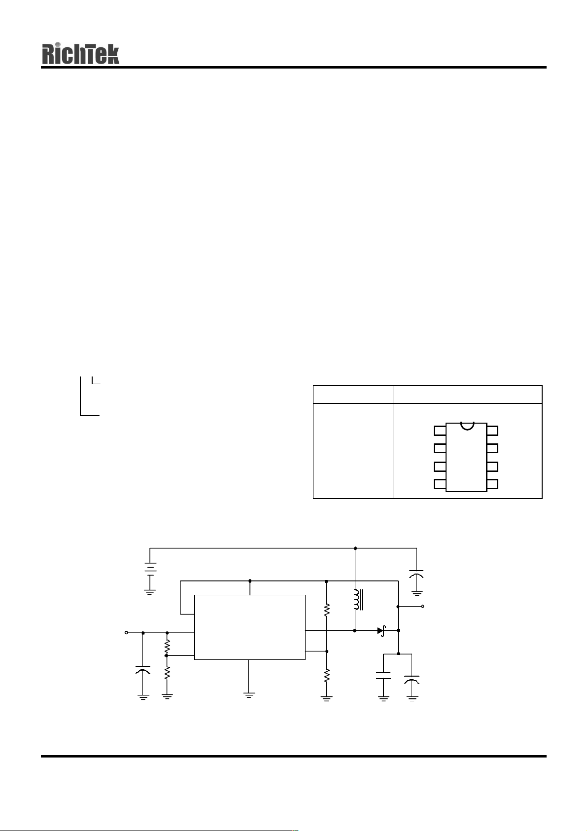
Typical Application Circuit
V
IN
CE
V
2.5V
OU T2
+
C3
10µF
Fig. 1 RT9264 Typical Application for Portable Instruments
LDOO LX
R4
42K
LFB GND FB
R3
22K
VDD
RT9264
EXT
R1
36K
R2
22K
L1
2.2µH
D1
1N5819
C2
1µF
LFB
LDOO
+
C1
47µF
3
4
47µF
3.3V
V
OU T1
6
VDD
5
FB
DS9264-00 December 2001 www.richtek-ic.com.tw
1

RT9264
Preliminary
V
IN
47µF
Chip Ena bl e I nput
3.3V
V
OU T
+
C3
10µF
VDD
CE
LDOO LX
LFB GND FB
RT9264
EXT
36K
22K
R1
R2
L1
2.2µH
D1
1N5819
C2
1µF
+
C1
47µF
Fig. 2 Application Circuit with Zero-Output-Current Shutdown Mode Control
R5
100
Ω
+
VDD
RT9264
C5
22µF
EXT
L1
3.3µH
D1
1N5819
Q1
NMOS
R1
220K
R2
20K
C4
47µF
C2
1µF
V
OU T2
3.3V/5 V
2.5V
C3
10µF
V
IN
CE
LDOO LX
R4
42K
+
LFB GND FB
R3
22K
+
15V
V
C1
47µF
OU T1
Fig. 3 High Voltage Application
www.richtek-ic.com.tw DS9264-00 December 2001
2

Pin Description
Preliminary
RT9264
Pin No. Pin Name
1GND
2EXT
Pin Function
Ground
Output pin for driving external NMOS or NPN
When driving an NPN, a resistor should be added for limiting base current.
3LFB
4LDOO
5FB
Feedback pin of the built-in LDO (Internal Vref = 0.86V)
Voltage output pin of the built-in LDO
Feedback input pin
Internal reference voltage for the error amplifier is 1.25V.
6VDD
7LX
8CE
Input positive power pin of RT9264
Pin for switching
Chip enable
RT9264 gets into shutdown mode when CE pin set to low.
Function Block Diagram
VDD
LDOO
LF B
FB
Q2
PMOS
VDD
VDD
1. 25 V
RT9264
_
1. 25 V
+
_
Loop Control Circuit
+
EXT
LX
Q1
NMOS
CE
R2
Q3
NMOS
Over Temp.
Detector
R1
Shut Down
GND
DS9264-00 December 2001 www.richtek-ic.com.tw
3
 Loading...