


VFM Step-Up DC/DC Converter
RT9261/A
General Description
The RT9261 Series are VFM Ste p-up DC/DC ICs with ultra
low supply current by CMOS process and suitable for
use with battery-powered instruments.
The RT9261 IC consists of an oscillator, a VFM control
circuit, a driver transistor (LX switch), a reference voltage
unit, an error a mplifier , resistors for voltage detection, a nd
a LX switch protection circuit. A low ripple and high
efficiency step-up DC/DC converter can be constructed of
this RT9261 IC with only three external components.
The RT9261A IC provides with a drive pin (EXT) for an
external transistor, so that a power transistor can be
externally applied. Therefore, the RT9261A IC is
recommended for a pplication s where large currents are
required. EN pin ena bles circuit to set the standby supply
current at a maximum of 0.5μA.
Ordering Information
RT9261/A-
Features
zz
Minimal Number of External Components ( Only
z
zz
an Inductor, a Diode, and a Capacitor)
zz
z Ultra Low Input Current ( 5
zz
±±
zz
z
±2% High Output V oltage Accura cy
zz
±±
zz
z Low Ripple and Low Noise
zz
zz
z Low Start-up Voltage, 0.85V at 1mA
zz
zz
z 75% Efficiency with Low Cost Inductor
zz
zz
z +50 ppm/
zz
zz
z SOT-89 and SOT-23-5 Small Pa c kages
zz
zz
z RoHS Compliant and 100% Lead (Pb)-Free
zz
°°
°C Low Temperature-Drift
°°
μμ
μA at Switch Off)
μμ
Applications
z Power source for battery-powered equipment
z Power source for ca mera s, ca mcorders, VCRs, PDAs,
pagers, electronic data ban ks, and ha nd-held
communication equipment
z Power source for a pplications, which require higher
voltage than that of batteries used in the a ppli ances
Package Type
B : SOT-23-5
X : SOT-89
Lead Plating System
P : Pb Free
G : Green (Halogen Free and Pb Free)
Output Voltage
15 : 1.5V
16 : 1.6V
:
49 : 4.9V
50 : 5.0V
Use external switch
Use internal switch
Note :
Richtek products are :
` RoHS compliant and compatible with the current require-
ments of IPC/JEDEC J-STD-020.
` Suitable for use in SnPb or Pb-free soldering processes.
Marking Information
For marking information, conta ct our sales representative
directly or through a Richtek distributor located in your
area.
Pin Configurations
(TOP VIEW)
123
GND
VOUT
RT9261
LX GND
5
EN VOUT NC
LX
(TAB)
SOT-89
4
23
SOT-23-5
123
EXT
VOUT
GND
(TAB)
RT9261A
EXT GND
5
EN VOUT NC
4
23
RT9261ART9261
DS9261/A-16 April 2011 www.richtek.com
1
RT9261/A
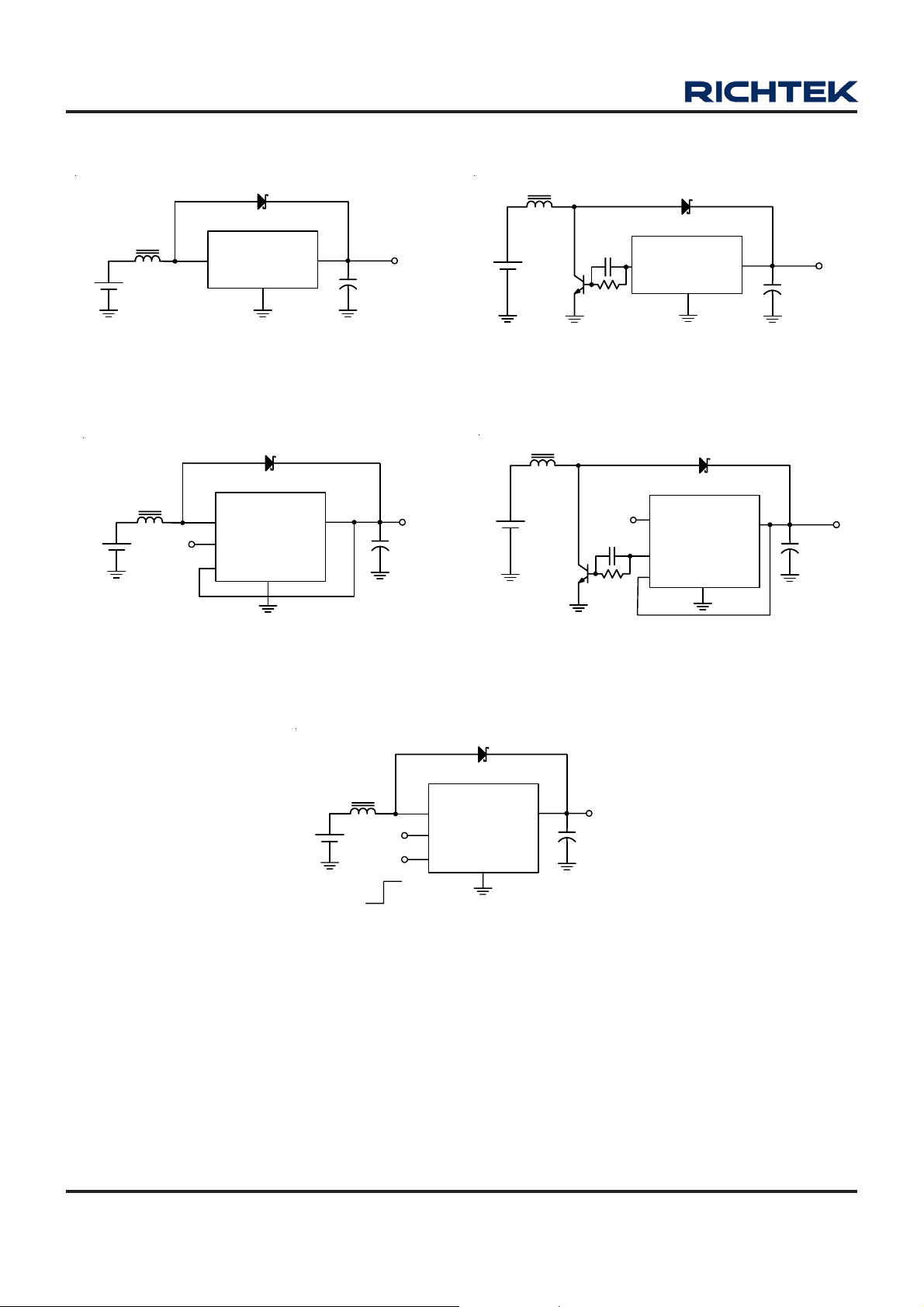
T ypical Application Circuit
D1
1N5819
L1
100µH
V
IN
RT9261xX
VOUTLX
GND
+
C
OUT
22µF
V
OUT
V
IN
L1
27µH
ZTX
650
0.01µF
Tr
Cb
Rb
300
D1
1N5819
RT9261AxX
VOUTEXT
GND
+
C
OUT
22µF
V
OUT
Figure 1 Figure 2
D1
1N5819
L1
100µH
V
IN
NC
RT9261xB
LX
EN
GND
VOUT
+
C
OUT
22µF
V
OUT
V
IN
L1
27µH
ZTX
650
0.01µF
Tr
Cb
Rb
300
NC
1N5819
RT9261AxB
EXT
EN
GND
D1
VOUT
+
C
OUT
22µF
V
OUT
Figure 3 Figure 4
D1
1N5819
L1
27µH
V
IN
NC
Chip
Enable
RT9261xB
LX
EN
GND
VOUT
+
C
OUT
22µF
V
OUT
Figure 5
DS9261/A-16 April 2011www.richtek.com
2

Functional Pin Description
RT9261/A
Pin No .
RT9261-□□□X RT9261A-□□□X RT9261-□□□B R T9261A-□□□B
1 1 4 4 GND Ground.
2 2 2 2 VOUT Output Voltage.
3 -- 5 -- LX Pin for Switching.
-- 3 -- 5 EXT Drive External Device.
-- -- 1 1 EN
-- -- 3 3 NC No Internal Connected.
Function Block Diagram
LX
LXSW
GND
EXT
VLX Limiter
Buffer
VFM Control
OSC 100kHz
+
Error
Amplifier
P in Name Pin Function
V
REF
Chip Enable (Active High).
VOUT
Notes:
(1) LX Pin...... only for 9261- xX and 9261- xB
(2) EXT Pin.... only for 9261A- xX a nd 9261A- xB
(3) EN Pin...... only for 9261- xB and 9261A- xB
Chip Enable
EN
DS9261/A-16 April 2011 www.richtek.com
3
RT9261/A
Absolute Maximum Ratings
z Output V oltage ------------------------------------------------------------------------------------------------------ 8V
z LX Pin V oltage
z EXT Pin V oltage
z EN Pin Voltage
z LX Pin Output Current
z EXT Pin Current
z Power Dissipation, P
SOT-89 ---------------------------------------------------------------------------------------------------------------- 0.5W
SOT-23-5-------------------------------------------------------------------------------------------------------------- 0.25W
z Pack age Thermal Resistance
SOT-89, θJC---------------------------------------------------------------------------------------------------------- 100°C/W
SOT -89, θJA---------------------------------------------------------------------------------------------------------- 300°C/W
SOT-23-5, θJA-------------------------------------------------------------------------------------------------------- 250°C/W
z Operating T emperature Range ----------------------------------------------------------------------------------- −20 to +85°C
z Storage T emperature Range-------------------------------------------------------------------------------------- 165°C
z Lead T emperature (Soldering, 10 sec.) ------------------------------------------------------------------------ 260°C
Notes:
(1) Applicable to R T9261- xX and RT9261- xB
(2) Applicable to R T9261A- xX and RT9261A- xB
(3) Applicable to RT9261- xB and RT9261A- xB
(1)
------------------------------------------------------------------------------------8V
(2)
------------------------------------------------------------------------------------------------- −0.3 to V
(3)
--------------------------------------------------------------------------------------------------- −0.3 to V
(1)
------------------------------------------------------------------------------------------ 250mA
(2)
-------------------------------------------------------------------------------------------------- ±50mA
@ T
D
= 25°C
A
OUT
OUT
+0.3V
+0.3V
Electrical Characteristics (Refer to Figure 1)
Parameter Symbol Test Conditions Min Typ Max Unit
Output Voltage Accuracy ΔV
In put Volt age VIN -- -- 7 V
Start - u p Volt a g e VST I
Hol d-on Voltage VHO I
In put Cu rr en t 1 V
In put Cu rr en t 2 V
LX Swi tc hing Curr e nt I
LX Lea ka ge Cu rr en t I
Maximum Oscillator F
Oscillator Duty Cycle D
Efficiency -- 75 -- %
VLX Voltage Limit LX switch on 0.65 0.8 1 V
Notes:
(1)Unless otherwise provided, V
(2)Unless otherwise provided, V
−2 -- 2 %
OUT
= 1mA, VIN: 0 → 2V -- 0.85 1 V
OUT
= 1mA, VIN: 2 → 0V 0.7 -- -- V
OUT
V
≤ 3.5V
at no load
IN
in switch off condition -- 5 8 μA
OUT
SWITCHING
LEAKAGE
MAX
OSC
= 1.8V, VSS = 0V, I
IN
= 3V, VSS = 0V, I
IN
V
V
80 120 160 kHz
On ( V
= 0.4V
LX
= 6V -- -- 0.5 μA
LX
” L ” ) side
LX
= 10mA, T
OUT
= 10mA, T
OUT
OUT
3.5V < V
V
≤ 3. 5V
OUT
3.5V < V
V
= 2.5V to 5V 65 75 85 %
OUT
= 1.5V to 2.4V 60 70 80 %
V
OUT
= 25°C, and External Circuit of Typical Application
OPT
= 25°C, and External Circuit of Typical Application
OPT
(1)
-- 15 18
(2)
OUT
OUT
≤ 5V
(1)
≤ 5V
-- 18 24
60 -- --
(2)
80 -- --
μA
mA
DS9261/A-16 April 2011www.richtek.com
4

Electrical Characteristics (Refer to Figure 2)
Parameter Symbol Test Conditions Min Typ Max Unit
RT9261/A
Output Voltage Accuracy ΔV
−2 -- +2 %
OUT
In put Volt age VIN -- -- 7 V
Start - u p Vo lt a g e VST I
In put Cu rre n t 1 V
In put Cu rre n t 2
EXT “H” Output Current V
EXT “L” Output Current V
Maxim um Os ci lla t or Fr equ en cy F
Oscillator Du ty Cycle D
80 120 160 kHz
MAX
V
OSC
= 1mA, V
OUT
at no load
IN
V
in switch off
OUT
condition
= V
EXT
= 0.4V
EXT
” H ” si de
EXT
OUT
: 0 → 2V -- 0.85 1.0 V
IN
– 0.4V
V
≤ 3.5V
OUT
3.5V < V
V
≤ 3.5V
OUT
3.5V < V
V
≤ 3.5V
OUT
3.5V < V
V
≤ 3.5V
OUT
3.5V < V
V
= 2.5V to 5V 65 75 85 %
OUT
= 1.5V to 2.4V 60 70 80 %
V
OUT
(1)
-- 30 50
(2)
OUT
OUT
OUT
OUT
≤ 5V
(1)
≤ 5V
(1)
≤ 5V
(1)
≤ 5V
-- 60 90
(2)
-- 6 10 μA
−1.5 -- --
(2)
−2 -- --
1.5 -- --
(2)
2 -- --
μA
mA
mA
Notes:
(1)Unless otherwise provided, V
Application
(2)Unless otherwise provided, V
= 1.8V, VSS = 0V, I
IN
= 3V, VSS= 0V, I
IN
OUT
= 10mA, T
OUT
= 10mA, T
= 25° C, and use External Circuit of Typical
OPT
= 25° C, and External Circuit of Typical Application
OPT
DS9261/A-16 April 2011 www.richtek.com
5

RT9261/A
Electrical Characteristics (Refer to Figure 3)
Parameter Symbol Test Conditions Min Typ Max Unit
Ou tput Voltag e Acc ur acy
Input Voltage
Start-up Voltage
Hold- o n Voltage
ΔV
OUT
V
IN
V
I
ST
V
I
HO
Efficiency
Input Current 1
Input Current 2
LX Switching Current
LX Leakage Current
I
SWITCHING
I
LEAKAGE
EN “H” Leve l
EN “ L” Level
EN “ H” Input Current
EN “ L“ Input Current EN = 0V
Maximum Oscillator Frequency
Oscillator Duty Cycle
V
Voltage Limit
LX
F
MAX
D
OSC
LX switch on 0.65 0.8 1.0 V
−2 -- +2 %
-- -- 7 V
= 1m A, V
OUT
= 1m A, V
OUT
V
≤ 3.5V
OUT
3.5V < V
V
at no load
IN
in switch
V
OUT
off condition
V
V
V
V
EN
LX
LX
IN
IN
= V
= 0.4V
= 6V
= V
OUT
= V
OUT
OUT
80 120 160 kHz
On (V
LX
side
OUT
× 0.9
× 0.9
” L” )
: 0 → 2V
IN
: 2 → 0V
IN
(1)
≤ 5V
V
OUT
3.5V < V
V
OUT
3.5V < V
V
OUT
3.5V < V
(2)
≤ 3.5V
≤ 3.5V
≤ 3.5V
OUT
OUT
OUT
(1)
≤ 5V
(1)
≤ 5V
(1)
≤ 5V
-- 0.85 1.0 V
0.7 -- -- V
-- 75 --
-- 85 --
-- 15 18
(2)
-- 18 24
-- 5 8
(2)
-- 6 10
60 -- --
(2)
80 -- --
-- -- 0.5
0.4 x
V
OUT
-- -- V
-- -- 0.2 V
-- -- 0.5 μA
−0.5
V
= 2.5V to 5V 65 75 85 %
OUT
= 1.5V to 2.4V 60 70 80 %
V
OUT
-- --
%
μA
μA
mA
μA
μA
Notes:
(1)Unless otherwise provided, V
Application
(2)Unless otherwise provided, V
= 1.8V, VSS = 0V, I
IN
= 3V, VSS= 0V, I
IN
OUT
= 10mA, T
OUT
= 10mA, T
= 25°C, and use External Circuit of Typical
OPT
= 25°C, and External Circuit of Typical Application
OPT
DS9261/A-16 April 2011www.richtek.com
6

RT9261/A
Electrical Characteristics (Refer to Figure 4)
Parameter Symbol Test Conditions Min Typ Max Unit
Output Voltage Accuracy ΔV
Input Voltage VIN -- -- 7 V
Start-up Voltage VST I
Efficiency
Input Current 1 V
Input Current 2
EXT “H” Output Current
EXT “L” Output Current V
EN “H” Level V
EN “ L” Level V
EN “ H” Input Current EN = V
EN “ L“ Input Current EN = 0V −0.5 -- -- μA
Maximum Oscillator Frequency F
Oscillator Duty Cycle D
V
Voltage Limit LX switch on 0.65 0.8 1.0 V
LX
Notes:
(1)Unless otherwise provided, V
Application
(2)Unless otherwise provided, V
= 1.8V, VSS = 0V, I
IN
= 3V, VSS= 0V, I
IN
−2 -- +2 %
OUT
= 1m A, V
OUT
V
≤ 3.5V
OUT
3.5V < V
IN
V
OUT
OUT
at no load
in switch
off condition
V
= V
EXT
OUT
0.4V
= 0.4V
EXT
= V
IN
OUT
= V
IN
OUT
OUT
80 120 160 kHz
MAX
OSC
On (V
side
LX
OUT
= 10mA, T
OUT
” L” )
= 10mA, T
: 0 → 2V -- 0.85 1.0 V
IN
(1)
-- 75 --
(2)
≤ 5V
–
× 0.9 0.4× V
-- 85 --
V
≤ 3.5V
OUT
3.5V < V
V
≤ 3.5V
OUT
3.5V < V
V
≤ 3.5V
OUT
3.5V < V
V
≤ 3.5V
OUT
3.5V < V
(1)
-- 30 50
(2)
OUT
OUT
OUT
OUT
≤ 5V
(1)
≤ 5V
(1)
≤ 5V
(1)
≤ 5V
-- 60 90
(2)
-- 6 10 μA
−1.5 -- --
(2)
−2 -- --
1.5 -- --
(2)
2 -- --
-- -- V
OUT
× 0.9 -- -- 0.2 V
-- -- 0.5 μA
V
= 2.5V to 5V 65 75 85 %
OUT
V
= 1.5V to 2.4V 60 70 80 %
OUT
= 25°C, and use External Circuit of Typical
OPT
= 25°C, and External Circuit of Typical Application
OPT
%
μA
mA
mA
DS9261/A-16 April 2011 www.richtek.com
7

RT9261/A
Typical Operating Characteristics
Start-up/Hold-on Voltage vs. Output Current
1.4
Start-up/Hold-on Voltage
1.2
0.8
0.6
Vstart/Vhold (V)
0.4
0.2
Vstart
1
Vhold
RT9261
V
0
0 1020304050
OUT
Output Current (mA)
Output Voltage vs. Output Current
3
2.5
1.5V
0.9V
2
1.0V
2.0V
= 2.7V
2.5V
Output Current v s. Ripple Voltage
120
100
80
2.0V
60
40
Ripple Voltage (mV p-p)
20
0
0 20406080100
1.5V
0.9V
RT9261
V
= 2.7V
OUT
2.5V
Output Current (mA)
Output Voltage vs. Temperature
2.90
2.85
2.80
1.5
1
Output Voltage (V)
0.5
0
020406080100
RT9261
V
= 2.7V
OUT
Output Current (mA)
Efficiency vs. Output Current
90
80
70
60
50
40
30
Efficiency (%)
20
10
0.9V
0
0 20406080100
1.5V
1.0V
2.0V
Output Current (mA)
RT9261
V
= 2.7V
OUT
2.5V
2.75
2.70
Output Voltage (V)
2.65
2.60
-40-200 20406080
Temperature
(°C)
RT9261
V
= 2.7V
OUT
Supply Current vs. Temperature
70
RT9261
V
= 2.7V
OUT
60
50
40
30
20
Supply Current (uA)
10
0
-40-200 20406080
Input Current 2
Temperature
Input Current 1
(°C)
DS9261/A-16 April 2011www.richtek.com
8

160
140
120
100
Maximum Oscillator Frequency
vs. Temperature
2.5
RT9261/A
Output Voltage v s. Output Current
3
2
1.0V
0.9V
2.5V
1.5V
2.0V
80
60
40
(°C)
RT9261
V
= 2.7V
OUT
20
0
Maximum Oscillator Frequency (kHz) A
-40 -20 0 20 40 60 80
Temperature
Oscillator Duty Cycle vs. Temperature
100
90
80
70
60
Oscillator Duty Cycle (%)
50
-40-200 20406080
Temperature
(°C)
RT9261
V
= 2.7V
OUT
1.5
1
Output Voltage (V)
0.5
0
0306090120150
RT9261A
V
= 2.7V
OUT
Output Current (mA)
Efficiency vs. Output Current
80
70
60
50
40
30
Efficiency (%)
20
10
0
0 306090120150
0.9V
1.0V
Output Current (mA)
2.5V
1.5V
RT9261A
V
= 2.7V
OUT
2.0V
Start -up/Hold- on Vo l tage vs. Output Current
1.6
1.4
1.2
1
0.8
0.6
Vstart
Vhold
Vstart/Vhold (V)
0.4
Start-up/Hold-on Voltage1
0.2
0
0 306090120150
RT9261A
V
= 2.7V
OUT
120
100
Ripple Voltage (mV p-p)
80
60
40
20
Output Current (mA)
Output Current vs. Ripple Voltage
2.5V
2.0V
1.5V
0.9V
RT9261A
V
= 2.7V
0
0306090120150
Output Current (mA)
OUT
DS9261/A-16 April 2011 www.richtek.com
9

RT9261/A
Outline Dimension
H
D
L
C
b
A
e
Dimensions In Millimeters Dimensions In Inches
Symbol
Min Max Min Max
A 0.889 1.295 0.035 0.051
A1 0.000 0.152 0.000 0.006
B 1.397 1.803 0.055 0.071
b 0.356 0.559 0.014 0.022
C 2.591 2.997 0.102 0.118
D 2.692 3.099 0.106 0.122
B
A1
10
e 0.838 1.041 0.033 0.041
H 0.080 0.254 0.003 0.010
L 0.300 0.610 0.012 0.024
SOT-23-5 Surface Mount Package
DS9261/A-16 April 2011www.richtek.com

D
D1
RT9261/A
A
C
B
C1
e
e
H
A
b
b1
Dimensions In Millimeters Dimension s In Inches
Symbol
Min Max Min Max
A 1.397 1.600 0.055 0.063
b 0.356 0.483 0.014 0.019
B 2.388 2.591 0.094 0.102
b1 0.406 0.533 0.016 0.021
C 3.937 4.242 0.155 0.167
b
C1 0.787 1.194 0.031 0.047
D 4.394 4.597 0.173 0.181
D1 1.397 1.753 0.055 0.069
e 1.448 1.549 0.057 0.061
H 0.356 0.432 0.014 0.017
3-Lead SOT-89 Surface Mount
Richtek Technology Corporation
Headquarter
5F, No. 20, Taiyuen Street, Chupei City
Hsinchu, Taiwan, R.O.C.
Tel: (8863)5526789 Fax: (8863)5526611
Information that is provided by Richtek Technology Corporation is believed to be accurate and reliable. Richtek reserves the right to make any change in circuit
design, specification or other related things if necessary without notice at any time. No third party intellectual property infringement of the applications should be
guaranteed by users when integrating Richtek products into any application. No legal responsibility for any said applications is assumed by Richtek.
DS9261/A-16 April 2011 www.richtek.com
Richtek Technology Corporation
Taipei Office (Marketing)
5F, No. 95, Minchiuan Road, Hsintien City
Taipei County, Taiwan, R.O.C.
Tel: (8862)86672399 Fax: (8862)86672377
Email: marketing@richtek.com
11

 Loading...