

Preliminary
RT9202
Single Synchronous Buck PWM DC-DC Controller
General Description
The RT9202 is a single power supply PWM DC-DC
converter controller designed to drive N-channel
MOSFET in a synchronous buck topology. The IC
integrates the control, output adjustment, monitoring
and protection functions in a small 8-pin package.
The RT9202 uses a low gain voltage mode PWM
control for simple application design. An internal 0.8V
reference allows the output voltage to be precisely
regulated to low voltage requirement. A fixed 300kHz
oscillator reduces the component size for saving
board space.
The RT9202 features over current protection, over
voltage protection, and under voltage lock-out. The
output current is monitored by sensing the voltage
drop across the MOSFET’s R
, which eliminates
DS(ON)
the need for a current sensing resistor.
Applications
Motherboard Power Regulation for Computers
z
Subsystems Power Supplies
z
Cable Modems, Set Top Box, and DSL Modems
z
DSP and Core Communications processor Supplies
z
Memory Power Supplies
z
Personal Computer Peripherals
z
Industrial Power Supplies
z
5V-Input DC-DC Regulators
z
Low Voltage Distributed Power Supplies
z
Features
z
Operate from 5V
z
0.8V Internal Reference
z
Drive Two N-channel MOSFET
z
Voltage Mode PWM Control
z
Fast Transient Response
z
Fixed 300kHz Oscillator Frequency
z
Full 0~100% Duty Cycle
z
Internal Soft Start
z
Adaptive Non-overlapping Gate Driver
z
Over-current Monitor Uses MOSFET R
z
Over-voltage Protection Uses Low-side
DS(ON)
MOSFET
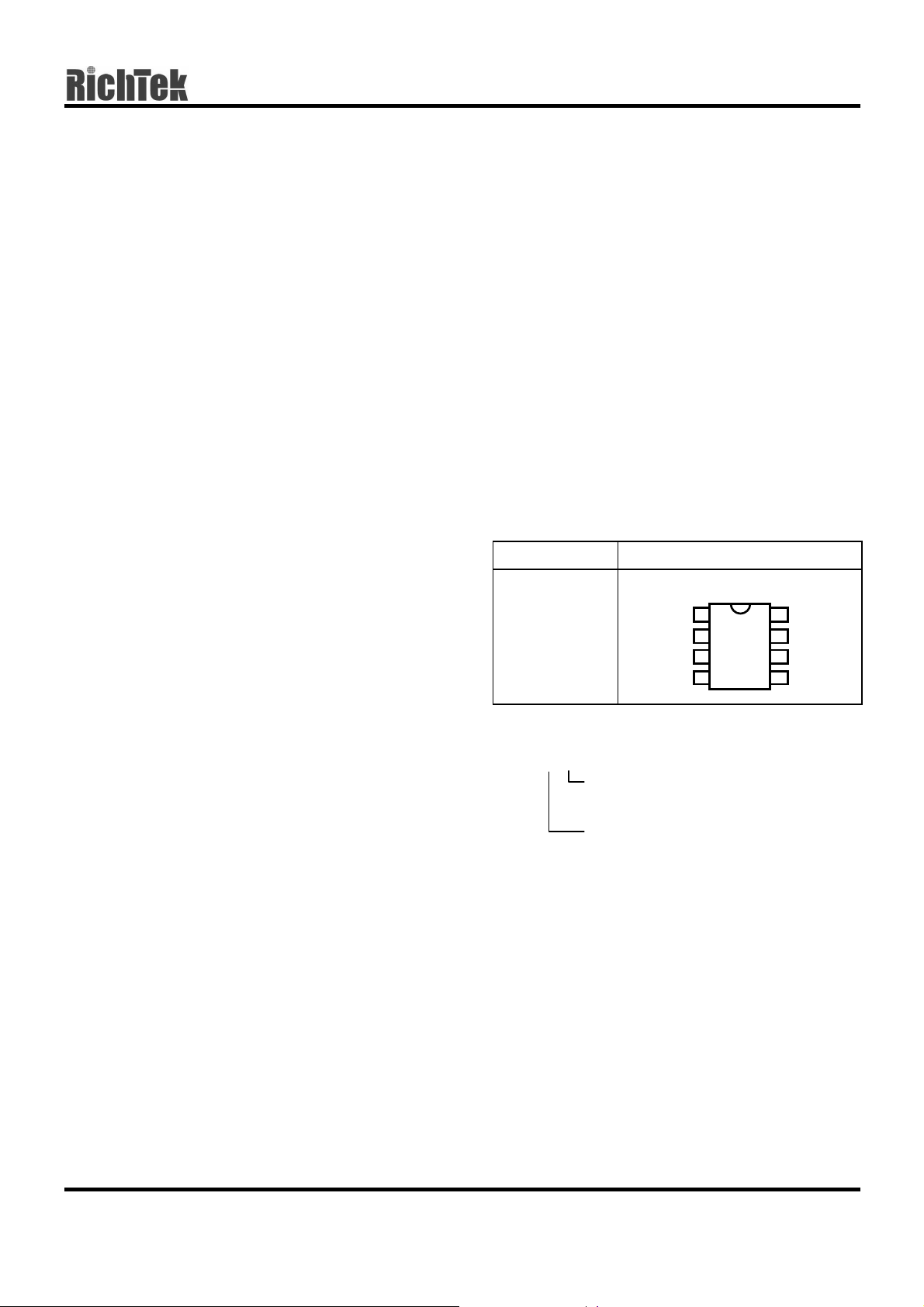
Pin Configurations
Part Number Pin Configurations
GND
TOP VIEW
1
2
3
4
8
7
6
5
PHASE
OCSET
FB
VCC
RT9202CS
(Plastic SOP-8)
BOO T
UGATE
LGATE
Ordering Information
RT9202
Package type
S : SOP-8
Operating temperature range
C: Commercial standard
DS9202-01 March 2002 www.richtek-ic.com.tw
1
RT9202
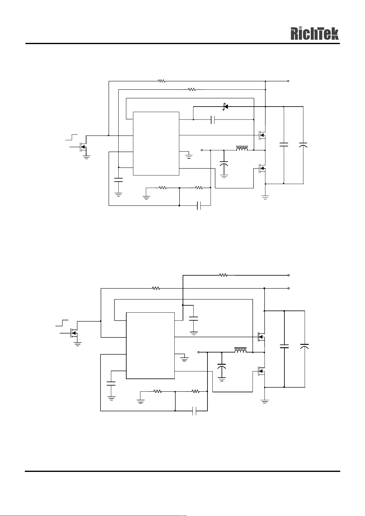
Typical Application Circuit
Preliminary
SHDN
H: shutdown
Q2
2N7002
R1
R4
10
V
2.5V
R2
255
C6
10nF
C2
0.1µF
OU T
1
2
3
4
C4
1µF
8
7
6
5
PHASE
OCSET
RT9202
FB
VCC
20K
BOOT
UGATE
GND
LGATE
R3
120
Fig.1 RT9202 powered from 5V only
D1
MA732
+
C3
1000µF
L2
5µH
MU
ML
5V
C5
1µF
+
C1
470µF
H: shutdown
SHDN
Q1
2N7002
C4
1µF
R1
20K
8
7
6
5
PHASE
OCSET
RT9202
FB
VCC
UGATE
LG ATE
R3
120
BOOT
GND
1
2
V
OU T
2. 5V
3
4
R2
250
C6
10nF
Fig.2 RT9202 powered from 12V
C2
1µF
R4
10
+
C3
1000µF
L1
5µH
MU
ML
12V
5V
C5
1µF
+
C1
470µF
www.richtek-ic.com.tw DS9202-01 March 2002
2
Preliminary
MU
+
COUT
CVCC
1µF
GND
VCC
RT9202
1000µF
CBOOT
BOOT
0.1µF
L
5µH
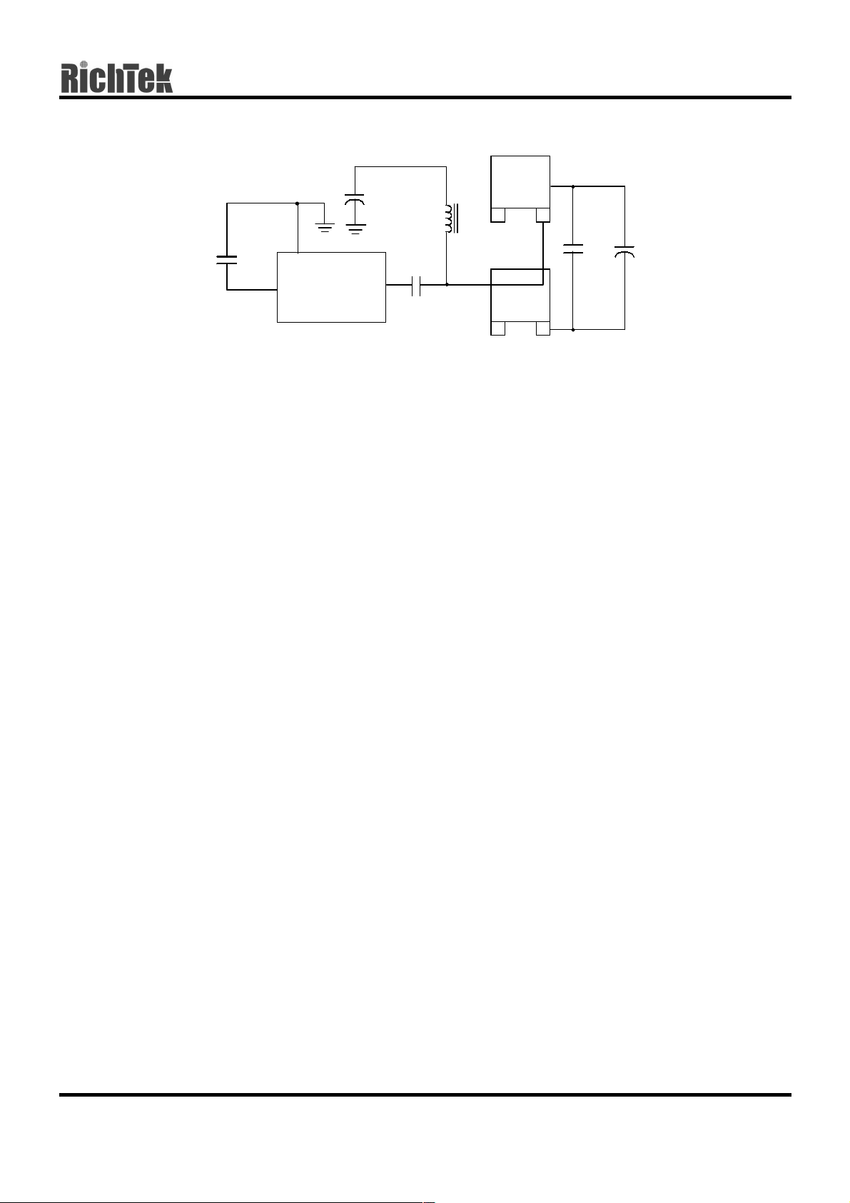
Layout Placement
Layout Notes
1. Put CIN1 & CIN2 to be near the MU drain and ML source nodes.
2. Put RT9202 to be near the COUT
3. Put CBOOT as close as to BOOT pin
4. Put CVCC as close as to VCC pin
D
GS
ML
D
GS
GND Re tur n
CIN1
1µF
+
RT9202
CIN2
470µF
DS9202-01 March 2002 www.richtek-ic.com.tw
3
RT9202
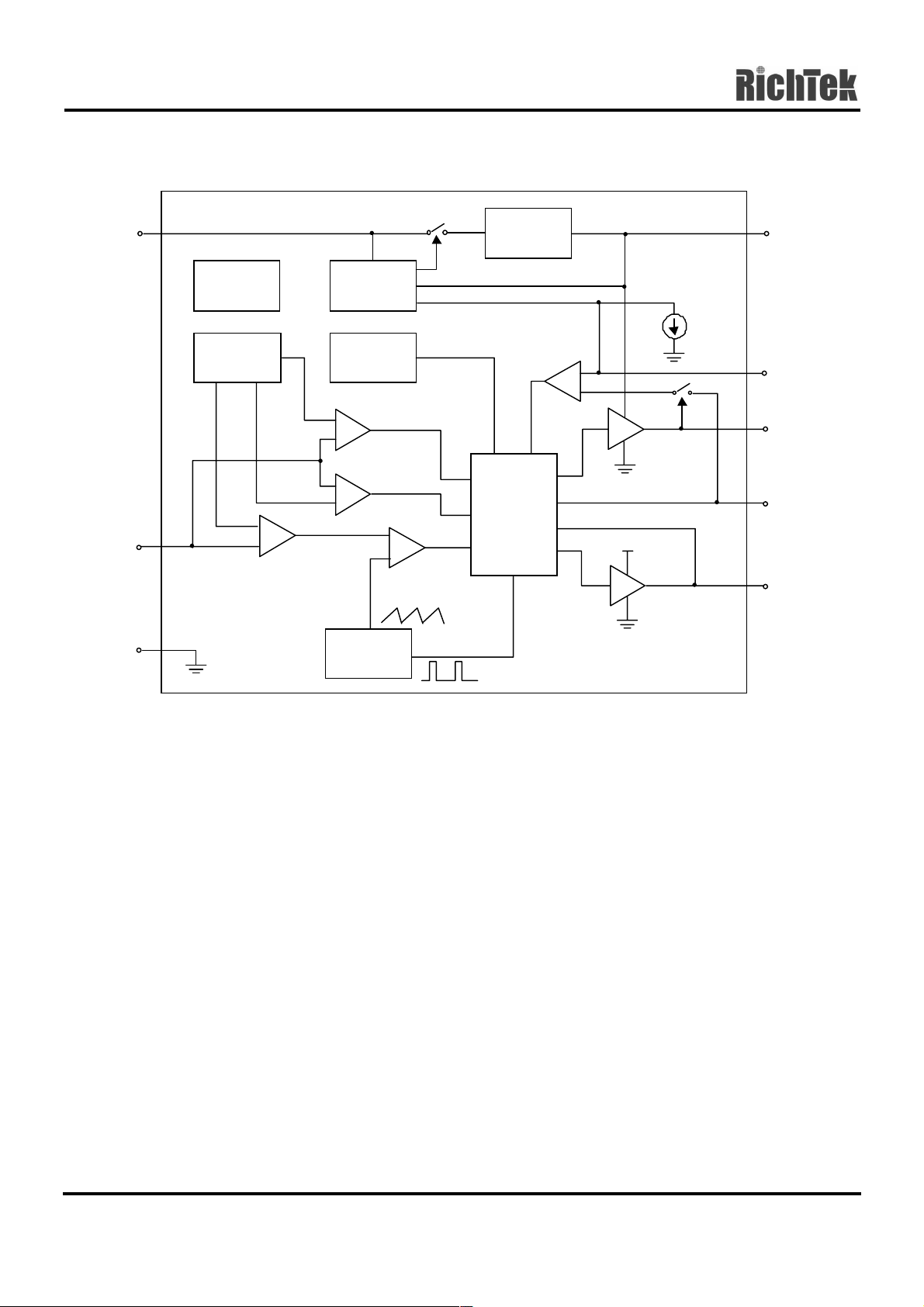
Function Block Diagram
Preliminary
VCC
FB
GND
Bias
0.8V
Reference
0.8V
Error
6.0V
Regulator
Power on
Reset
40µA
Soft Start
+
OC
_
1V
0.5V
+
35dB
_
Erro r
Amp
_
OVP
+
_
UVP
+
300kH z
Oscillator
+
PWM
_
Control
Logic
VCC
BOOT
OCSET
UGATE
PHASE
LGATE
www.richtek-ic.com.tw DS9202-01 March 2002
4

Preliminary
RT9202
Absolute Maximum Ratings
z
Supply Voltage VCC 7V
z
BOOT & UGATE to GND 15V
z
Input, Output or I/O Voltage GND−0.3V ~ 7V
z
Power Dissipation, PD @ TA = 25°C
SOP-8 0.625W
z
Package Thermal Resistance
SOP-8, θ
z
Ambient Temperature Range 0°C ~ +70°C
z
Junction Temperature Range -40°C ~ +125°C
z
Storage Temperature Range -65°C ~ +150°C
z
Lead Temperature (Soldering, 10 sec.) 260°C
JA
160°C/W
CAUTION:
Stresses beyond the ratings specified in “Absolute Maximum Ratings” may cause permanent damage to the
device. This is a stress only rating and operation of the device at these or any other conditions above those
indicated in the operational sections of this specification is not implied.
Electrical Characteristics
(V
= 5V, TA = 25°C, Unless otherwise specified.)
CC
Parameter Symbol Test Conditions Min Typ Max Units
VCC Supply Current / Regulated Voltage
Nominal Supply Current
Regulated Voltage from BOOT
I
V
CC
CC
UGATE, LGATE open -- 3 -- mA
V
BOOT
= 12V
-- 6.0 -- V
Power-On Reset
Rising VCC Threshold
VCC Threshold Hysteresis
Rising V
OCSET
Threshold
V
OCSET
V
OCSET1
= 4.5V
= 4.5V
3.85 4.1 4.35 V
0.3 0.5 0.7 V
0.8 1.25 2.0 V
Reference
Reference Voltage 0.784 0.8 0.816 V
Oscillator
Free Running Frequency 250 300 350 KHz
Ramp Amplitude
∆ V
OSC
-- 1.9 --
Error Amplifier
DC gain -- 35 -- dB
PWM Controller Gate Driver
V
P-P
Upper Drive Source
Upper Drive Sink
Lower Drive Source
Lower Drive Sink
R
UGATE
R
UGATE
R
LGATE
R
LGATE
BOOT= 12V
BOOT-V
V
UGATE
VCC - V
V
LGATE
UGATE
= 1V
LGATE
= 1V
= 1V
= 1V,
-- 7 --
-- 5 --
-- 4 --
-- 2 --
Ω
Ω
Ω
Ω
To be continued
DS9202-01 March 2002 www.richtek-ic.com.tw
5

RT9202
Parameter Symbol Test Conditions Min Typ Max Units
Protection
FB Over-Voltage Trip FB Rising -- 1 -- V
FB Under-Voltage Trip FB Falling -- 0.5 -- V
Preliminary
OCSET Current Source I
Soft-Start Interval -- 2 -- mS
OCSET
V
OCSET
= 4.5V -- 40 -- µA
Functional Pin Description
BOOT (Pin 1)
This pin provides ground referenced bias voltage to the
upper MOSFET driver. A bootstrap circuit is used to
create a voltage suitable to drive a logic-level N-
channel MOSFET when operating at a single 5V power
supply. This pin also could be powered from ATX 12V,
in this situation, a internal 6.0V regulator will supply to
VCC pin for internal voltage bias.
UGATE (Pin 2)
Connect UGATE pin to the PWM converter’s upper
MOSFET gate. This pin provides the gate drive for the
upper MOSFET.
GND (Pin 3)
Signal and power ground for the IC. All voltage levels
are measured with respect to this pin.
LGATE (Pin 4)
Connect LGATE to the PWM converter’s lower
MOSFET gate. This pin provides the gate drive for the
lower MOSFET.
FB (Pin 6)
This pin is connected to the PWM converter’s output
divider. This pin also connects to internal PWM error
amplifier inverting input and protection monitor.
OCSET (Pin 7)
Connect a resistor from this pin to the drain of the
respective upper MOSFET. This resistor, an internal
40µA current source, and the upper MOSFET on-
resistance set the converter over-current trip point. An
over-current trip cycles the soft-start function. The
voltage at this pin is monitored for power-on reset
(POR) purpose and pulling this pin low with an open
drain device will shut down the IC.
RI
×
I
=
PEAK
PHASE (Pin 8)
This pin is used to monitor the voltage drop across the
upper MOSFET for over-current protection.
OCSETOCSET
R
)ON(DS
VCC (Pin 5)
This is the main bias supply for the RT9202. This pin
also provides the gate bias charge for the lower
MOSFETs gate. The voltage at this pin monitored for
power-on reset (POR) purpose. This pin is also the
internal 6.0V regulator output powered from BOOT pin
when BOOT pin is directly powered from ATX 12V.
www.richtek-ic.com.tw DS9202-01 March 2002
6

Typical Operating Charateristics
Dead Time Dead Time
Preliminary
RT9202
UGATE
VCC = 5V
V
= 2.2V
OUT
Time
Power On
V
CC
LGATE
= 5V
V
CC
LGATE
Time
Power Off
V
CC
VCC = 5V
VCC = 5V
V
OUT
UGATE
= 2.2V
Time
Load Transient
UGATE
V
OUT
V
V
C
CC
OUT
OUT
V
= 5V
= 2.2V
= 3000µF
OUT
V
OUT
Time
Load Transient
UGATE
V
V
C
V
OUT
CC
OUT
OUT
= 5V
= 2.2V
= 3000µF
Time
DS9202-01 March 2002 www.richtek-ic.com.tw
Time
7

RT9202
µ
Preliminary
Reference (V)
0.803
0.802
0.801
0.800
0.799
0.798
Bootstrap Wave Form
= 5V; V
V
CC
OUT
UGATE
LGATE
PHASE
Time
Reference vs. Temperature
= 2.2V
( A)
OCSET
I
55
50
45
40
35
30
Short Hiccup
I
vs. Temperature
OCSET
Time
V
OUT
UGATE
VCC = 5V
V
= 2.2V
OUT
0.797
0.796
-50 0 50 100 150
Temperature ( C)
°
POR (Rising/Falling) vs. Temperature
4.3
4.2
4.1
4.0
3.9
POR (V)
3.8
Rising
Falling
3.7
3.6
-50 0 50 100 150
Temperature ( C)
°
25
20
-40 -10 20 50 80 110 140
Temperature ( C)
°
Oscillator Frequency vs. Temperature
315
310
305
300
295
290
285
Frequency (kHz)
280
275
270
-50 0 50 100 150
Temperature ( C)
°
www.richtek-ic.com.tw DS9202-01 March 2002
8

Functional Description
Preliminary
RT9202
The RT9202 operates at either single 5V power
supply with a bootstrap UGATE driver or 5V/12V
dual-power supply form the ATX SMPS. The dual-
power supply is recommended for high current
application, the RT9202 can deliver higher gate
driving current while operating with ATX SMPS based
on dual-power supply.
The Bootstrap Operation
In a single power supply system, the UGATE driver of
RT9202 is powered by an external bootstrap circuit,
as the Fig.1. The boot capacitor, C
, generates a
BOOT
floating reference at the PHASE pin. Typically a
0.1µF C
is enough for most of MOSFETs used
BOOT
with the RT9202. The voltage drop between BOOT
and PHASE is refreshed to a voltage of VCC – diode
drop (V
C2
1µF
) while the low side MOSFET turning on.
D
R1
VCC
BOOT
UGATE
PHASE
D1
0.1µF
+
5V
C1
1µF
R1
10
12V
+
VCC
C2
1µF
6.0 V
Regulator
RT9202
BOOT
UGATE
VCC
LGATE
Fig.2 Dual Power Supply Operation
Power On Reset
The Power-On Reset (POR) monitors the supply
voltage (normal +5V) at the VCC pin and the input
voltage at the OCSET pin. The VCC POR level is
4.1V with 0.5V hysteresis and the normal level at
OCSET pin is 1.5V (see over-current protection). The
POR function initiates soft-start operation after all
supply voltages exceed their POR thresholds.
5V
VCC
LGATE
RT9202
Fig.1 Single 5V power Supply Operation
Dual Power Operation
The RT9202 was designed to regulate a 6.0V at VCC
pin automatically when BOOT pin is powered by 12V.
In a system with ATX 5V/12V power supply, the
RT9202 is ideal for higher current application due to
the higher gate driving capability, V
V
= 6.0V. A RC (10Ω/1µF) filter is also
LGATE
UGATE
= 7V and
recommended at BOOT pin to prevent the ringing
induced from fast power on, as shown in Fig.2.
Soft Start
A built-in soft-start is used to prevent surge current
from power supply input during power on. The soft-
start voltage is controlled by an internal digital
counter. It clamps the ramping of reference voltage at
the input of error amplifier and the pulse-width of the
output driver slowly. The typical soft-start duration is
2mS.
Over-Current Protection
The over current protection (OCP) function of the
RT9202 is triggered when the voltage across the
R
of upper side MOSFET that developed by
DS(
ON)
drain current exceeds over-current tripping level. An
external resistor (R
) programs the over-current
OCSET
tripping level of the PWM converter. As shown on
Fig.1, the internal 40µA current sink (I
a voltage across R
V
. The DRIVE signal enables the over-current
IN
OCSET
(V
) that is referenced to
SET
OCSET
) develops
comparator (OC). When the voltage across the upper
MOSFET (V
) exceeds V
DS(ON)
, the over-current
SET
DS9202-01 March 2002 www.richtek-ic.com.tw
9

RT9202
Preliminary
comparator trips to set the over-current latch. Both
V
and VDS are referenced to VIN and a small
SET
capacitor across R
variations of V
due to MOSFET switching. The
IN
OCSET
helps V
tracking the
OCSET
over-current function will be tripped at a peak
inductor current (I
) determined by:
PEAK
COUNT = 1 COUNT = 2 COUNT = 3
4V
SS
2V
Internal
0V
OVERLOAD
APPLIED
The OC trip point varies with MOSFET’s R
DS(ON)
temperature variations. The temperature coefficient
of I
R
DS(ON)
is 2500ppm that is used to compensate
OCSET
temperature variations. To avoid over-current
tripping in the normal operating load range,
determine the R
resistor value from the equation
OCSET
above with:
1. The maximum R
at the highest junction
SD(ON)
temperature
2. The minimum I
3. Determine I
PEAK
from the characteristics
OCSET
for I
PEAK
> I
OUT(MAX)
+ (∆I)/2
where ∆I is the output inductor ripple current.
OVE R-CURRE NT TRIP:
V
V
>
DS
SET
R
iD
OC
×
PWM
DS(ON)
+
_
> I
CONTROL
OCSET
GATE
OCSET
I
OCSET
40µA
DRIVE
× R
OCSET
VCC
R
V
UGATE
PHASE
V
PH ASE
V
OC SET
OCSET
SET +
= V
= V
V
= +5V
IN
i
D
V
DS+
- V
IN
DS
- V
IN
SET
0A
INDUCTOR CURRENT
T0T1 T2
TIME
T3
Fig. 4
Shutdown
Pulling low the OCSET pin by a small single
transistor can shutdown the RT9202 PWM controller
as shown in typical application circuit.
Fig.3
Under Voltage and Over Voltage Protection
The voltage at FB pin is monitored and protected
against OC (over current), UV (under voltage), and
OV (over voltage). The UV threshold is 0.5V and OV-
threshold is 1.0V. Both UV/OV detection have 30µS
triggered delay. When OC or UV trigged, a hiccup re-
start sequence will be initialized, as shown in Fig.4.
Only 3 times of trigger are allowed to latch off. Hiccup
is disabled during soft-start interval.
www.richtek-ic.com.tw DS9202-01 March 2002
10

Applications Information
Preliminary
RT9202
Inductor Selection
The RT9202 was designed for V
= 5V, step-down
IN
application mainly. Fig.5 shows the typical topology
and waveforms of step-down converter.
The ripple current of inductor can be calculated as
follows:
IL
RIPPLE
= (5V - V
OUT
)/L × T
ON
Because operation frequency is fixed at 300kHz,
T
The V
V
= 3.33 × V
ON
ripple is
OUT
OUT RIPPLE
= IL
OUT
RIPPLE
/5V
× ESR
ESR is output capacitor equivalent series resistor
Table 1 shows the ripple voltage of V
: VIN = 5V
OUT
V
I
V
i
C.C.M.
L
L
Q
T
S
T
ONTOFF
V
I - VO
L
V
L
DC
-
VO
I
µ
L
V
R
O
Q
µ
IL = I
O
i
Q
i
D
Fig.5
Table 1
V
OUT
3.3V 2.5V 1.5V
Inductor 2µH5µH2µH5µH2µH5µH
1000µF (ESR=53mΩ) 100mV 40mV 110mV 44mV 93mV 37mV
1500µF (ESR=33mΩ) 62mV 25mV 68mV 28mV 58mV 23mV
3000µF (ESR=21mΩ) 40mV 16mV 43mV 18mV 37mV 15mV
*Refer to Sanyo low ESR series (CE, DX, PX…)
The suggested L and C are as follows:
2µH with ≥ 1500µF C
5µH with ≥ 1000µF C
OUT
OUT
I
Q
I
D
DS9202-01 March 2002 www.richtek-ic.com.tw
11

RT9202
Preliminary
Input / Output Capacitor
High frequency/long life decoupling capacitors should
be placed as close to the power pins of the load as
physically possible. Be careful not to add inductance
to the PCB trace, as it could eliminate the
performance from utilizing these low inductance
components. Consult with the manufacturer of the
load on specific decoupling requirements.
The output capacitors are necessary for filtering
output and stabilizing the close loop (see the PWM
loop stability). For powering advanced, high-speed
processors, it is required to meet with the
requirement of fast load transient, high frequency
capacitors with low ESR/ESL capacitors are
recommended.
Another concern is high ESR induced ripple may
trigger UV or OV protections.
PWM Loop Stability
The RT9202 is a voltage mode buck controller
designed for 5V step-down applications. The gain of
error amplifier is fixed at 35dB for simplified design.
The output amplitude of ramp oscillator is 1.6V, the
loop gain and loop pole/zero are calculated as
follows:
DC loop gain G
LC filter pole P
A
O
Error Amp pole P
ESR zero Z
= × π × ESR × C
O
= 35dB × ×
1
= × π ×
2
= 300kHz
A
5
6.1
LC
1
2
8.0
VOUT
The RT9202 Bode plot as shown Fig.6 is stable in
most of application conditions.
= 3.3V
V
OU T
C
= 1500µF(33mΩ)
OUT
L=2µH
= 2.9kH z
40
30
V
V
OU T
OU T
= 2.5V
= 3.3V
= 1.5V
V
OU T
P
O
= 3.2kHz
Z
O
Reference Voltage
Because RT9202 use a low 35dB gain error amplifier,
shown in Fig. 7. The voltage regulation is dependent
on V
0.8V were trimmed at V
condition. In a fixed V
reference voltage vs. V
IN
& V
setting. The FB reference voltage of
OUT
= 5V & V
IN
= 5V application, the FB
IN
voltage can be calculated
OUT
OUT
= 2.5V
as Fig. 8.
I3
FB
+
_
I2
1K
REP
0.8V
_
EA
+
1.75 V
56K
RAMP
+
PWM
_
Fig. 7
0.8 2
VIN = 5V
43.531 1.5 2 2.5
FB (V)
0.8 1
0.8 0
0.7 9
0.7 8
0.5
V
OUT
(V)
Fig. 8
Feedback Divider
The reference of RT9202 is 0.8V. The output voltage
can be set using a resistor based divider as shown in
Fig.9. Put the R1 and R2 as close as possible to FB
pin and R2 should less than 1 kΩ to avoid noise
coupling. The C1 capacitor is a speed-up capacitor
for reducing output ripple to meet with the
requirement of fast transient load. Typically a 1nF ~
0.1µF is enough for C1.
4.5
20
10
Loop Ga in
1M100k10k1k100
Fig. 6
www.richtek-ic.com.tw DS9202-01 March 2002
12

Preliminary
RT9202
VIN
L
V
R1
R2
<
OUT
1K
C1
RT9202
FB
+
C
OUT
Fig. 9
PWM Layout Considerations
MOSFETs switch very fast and efficiently. The speed
with which the current transitions from one device to
another causes voltage spikes across the
interconnecting impedances and parasitic circuit
elements. The voltage spikes can degrade efficiency
and radiate noise, that results in ocer-voltage stress
on devices. Careful component placement layout and
printed circuit design can minimize the voltage spikes
induced in the converter. Consider, as an example,
the turn-off transition of the upper MOSFET prior to
turn-off, the upper MOSFET was carrying the full load
current. During turn-off, current stops flowing in the
upper MOSFET and is picked up by the low side
MOSFET or Schottky diode. Any inductance in the
switched current path generates a large voltage spike
during the switching interval. Careful component
selections, layout of the critical components, and use
shorter and wider PCB traces help in minimizing the
magnitude of voltage spikes.
There are two sets of critical components in a DC-DC
converter using the RT9202. The switching power
components are most critical because they switch
large amounts of energy, and as such, they tend to
generate equally large amounts of noise. The critical
small signal components are those connected to
sensitive nodes or those supplying critical bypass
current.
especially the high-frequency ceramic decoupling
capacitors, close to the power switches. Place the
output inductor and output capacitors between the
MOSFETs and the load. Also locate the PWM
controller near by MOSFETs.
A multi-layer printed circuit board is recommended.
Fig.10 shows the connections of the critical
components in the converter. Note that the capacitors
CIN and COUT each of them represents numerous
physical capacitors. Use a dedicated grounding plane
and use vias to ground all critical components to this
layer. Apply another solid layer as a power plane and
cut this plane into smaller islands of common voltage
levels. The power plane should support the input
power and output power nodes. Use copper filled
polygons on the top and bottom circuit layers for the
PHASE node, but it is not necessary to oversize this
particular island. Since the PHASE node is subjected
to very high dV/dt voltages, the stray capacitance
formed between these island and the surrounding
circuitry will tend to couple switching noise. Use the
remaining printed circuit layers for small signal
routing. The PCB traces between the PWM controller
and the gate of MOSFET and also the traces
connecting source of MOSFETs should be sized to
carry 2A peak currents.
IL
IQ2
VCC GND
RT9202
+
FB
V
OUT
+
GND
5V
IQ1
Q1
+
Q2
LGATE
UGATE
Fig. 10
LOAD
The power components and the PWM controller
should be placed firstly. Place the input capacitors,
DS9202-01 March 2002 www.richtek-ic.com.tw
13

RT9202
Package Information
B
J
Preliminary
H
A
M
F
C
D
Dimensions In Millimeters Dimensions In Inches
Symbol
Min Max Min Max
A 4.801 5.004 0.189 0.197
B 3.810 3.988 0.150 0.157
C 1.346 1.753 0.053 0.069
D 0.330 0.508 0.013 0.020
F 1.194 1.346 0.047 0.053
H 0.178 0.254 0.007 0.010
I 0.102 0.254 0.004 0.010
J 5.791 6.198 0.228 0.244
M 0.406 1.270 0.016 0.050
I
www.richtek-ic.com.tw DS9202-01 March 2002
14

Preliminary
RT9202
DS9202-01 March 2002 www.richtek-ic.com.tw
15

RT9202
Preliminary
RICHTEK TECHNOLOGY CORP.
Headquarter
6F, No. 35, Hsintai Road, Chupei City
Hsinchu, Taiwan, R.O.C.
Tel: (8863)5510047 Fax: (8863)5537749
www.richtek-ic.com.tw DS9202-01 March 2002
16
RICHTEK TECHNOLOGY CORP.
Taipei Office (Marketing)
8F-1, No. 137, Lane 235, Paochiao Road, Hsintien City
Taipei County, Taiwan, R.O.C.
Tel: (8862)89191466 Fax: (8862)89191465
Email: marketing@richtek-ic.com.tw
 Loading...