

Single Synchronous Buck Controller
RT8204L
General Description
The RT8204L PWM controller provides high efficiency,
excellent transient response, and high DC output accuracy
needed for stepping down high voltage batteries to
generate low voltage CPU core, I/O, and chipset RAM
supplies in notebook computers.
The constant-on-time PWM control scheme handles wide
input/output voltage ratios with ease and provides 100ns
“instant-on” response to load transients while maintaining
a relatively constant switching frequency.
The RT8204L achieves high efficiency at a reduced cost
by eliminating the current sense resistor found in
traditional current mode PWMs. Efficiency is further
enhanced by its ability to drive very large synchronous
rectifier MOSFETs. The buck conversion allows this device
to directly step down high voltage batteries for the highest
possible efficiency. The RT8204L is intended for CPU core,
chipset, DRAM, or other low voltage supplies as low as
0.75V. The RT8204L is available in a WQFN-16L 3x3
package.
A built in LDO controller can drive an external N-MOSFET
to provide a second output voltage from PWM output or
other power source. The RT8204L can provide adjustable
voltage down to 0.75V and maximum output voltage is
dependen on the selected MOSFET. The internal 0.75V
reference voltage with ±1.5% accuracy provides tight
regulation of the output voltage. Other features such as
independent enable control, open drain power good
indicator, under voltage protection, and soft start make
the RT8204L a system friendly power management solution
for various applications.
Features
zz
PWM Controller
z
zz
``
` Ultra High Efficiency
``
``
` Resistor Progra mmable Current Limit by Low Side
``
R
``
` 4700ppm/
``
``
` Quick Load Step Response within 100ns
``
``
` 1% V
``
``
` Adjustable 0.75V to 3.3V Output Range
``
``
` 4.5V to 26V Battery Input Range
``
``
` Resistor Programmable Frequency
``
``
` Integrated Bootstrap Switch
``
``
` Over/Under Voltage Protection
``
``
` Voltage Ramp Soft-Start
``
``
` Power Good Indicator
``
zz
z LDO Controller
zz
``
` 1.5% accuracy Over Line and Load
``
``
` Independent Enable and Power Good Indicator
``
``
` Drive N-MOSFETs within Rail to Rail Controller
``
Sense (Lossless Limit)
DS(ON)
°°
°C R
°°
Accuracy Over Line and Load
FB
Current Sensing
DS(ON)
Voltage
``
` MLCC and POSCAP Stable
``
zz
z RoHS Compliant and Halogen Free
zz
Applications
z Notebook Computers
z CPU Core Supply
z Chipset/RAM Supply as Low as 0.75V
Ordering Information
RT8204L
Package Type
QW : WQFN-16L 3x3 (W-Type)
Lead Plating System
G : Green (Halogen Free and Pb Free)
Z : ECO (Ecological Element with
Halogen Free and Pb free)
Note :
Richtek products are :
` RoHS compliant and compatible with the current require-
ments of IPC/JEDEC J-STD-020.
` Suitable for use in SnPb or Pb-free soldering processes.
DS8204L-04 April 2011 www.richtek.com
1
RT8204L
Marking Information
RT8204LGQW
J8= : Product Code
YMDNN : Data Code
J8=YM
DNN
RT8204LZQW
J8 : Product Code
YMDNN : Data Code
J8 YM
DNN
Typical Application Circuit
Pin Configurations
VOUT
VDD
FB
PGOOD
V
N
I
V
5
.
4
o
2
t
6
V
R
T
O
N
(TOP VIEW)
TON
EN/DEM
BOOT
LEN
13141516
1
2
GND
3
4
WQFN-16L 3x3
17
LFB
LDRV
LPGOOD
8765
LGATE
12
11
10
9
UGATE
PHASE
OC
VDDP
C
R
T
8
0
2
4
16
O
N
T
V
P
D
D
V
5
O
G
P
C
C
D
M
/
D
O
L
E
n
a
L
P
D
O
G
O
V
1
C
D
O
M
E
b
e
l
O
D
D
D
P
1
R
3
R
17 (Exposed Pad)
:
*
O
p
o
i
t
9
V
D
D
P
2
R
2
D
D
V
2
C
4
O
O
G
P
15
E
D
N
E
/
14
L
E
N
5
L
P
O
G
D
G
N
n
a
l
L
B
O
T
O
U
G
A
T
E
P
H
S
A
E
L
G
A
T
E
O
C
D
M
O
D
F
B
V
O
U
T
L
D
R
V
L
F
B
13
12
11
8
10
3
1
7
6
R
4
C
R
5
R
I
I
L
M
R
C
3
Q
Q
2
3
Q
R
1
9
0
R
1
C
1
9
1
0
R
1
2
4
V
O
U
T
1
1
L
1
6
R
*
R
7
C
5
*
C
1
C
1
2
1
*
C
6
*
R
8
C
C
V
O
U
T
1
3
C
8
7
*
C
1
4
2
DS8204L-04 April 2011www.richtek.com
2
Function Block Diagram
TRIG
+
+
GM
-
-
SS Ramp
On-time
Compute
1-SHOT
+
-
+
-
90% V
OV
UV
VOUT
TON
FB
VDD
GND
SS (Internal)
115% V
70% V
REF
REF
+
Latch
S1 Q
Latch
S1 Q
REF
Thermal
Shutdown
Comp
+
R
QS
Min. T
OFF
QTRIG
1-SHOT
Emulation
Diode
RT8204L
BOOT
DRV
DRV
20µA
+
-
UGATE
PHASE
VDDP
LGATE
PGND
OC
EN/DEM
LEN
LFB
0.75V V
SS Ramp
90% V
50% V
REF
+
-
+
REF
-
REF
+
LDO Controller
SS
X1
PGOOD
LDRV
LPGOOD
DS8204L-04 April 2011 www.richtek.com
3

RT8204L
Functional Pin Description
Pin No. Pin Name Pin Function
1 VOUT
2 VDD
3 FB
4 PGOOD
5 LPGOOD
6 LFB
7 LDRV Drive Signal for LDO’s Path MOSFET.
8 LGATE
9 VDDP
10 OC
11 PHASE
12 UGATE
13 BOOT
14 LEN
15 EN/DEM
16 TON
17 (Exposed Pad) GND
Output Voltage Sense Pin. Connect this pin to the output of the PWM converter.
VOUT is an inp ut of the PWM controller.
Analog Supply Voltage Inpu t for Internal Analog In tegrated Circuit. Bypass this
pin to GND with a 1μF ceramic capacitor.
Feedback Input o f PWM Cont roll er. Conn ect FB to a resistive voltage divider
from VOUT to GND t o adjust the output voltage from 0.75V to 3 .3V.
Power Good Signal Open-Drain Output of PW M Cont roller. Th is pin will be
pulled high when the ou tput voltage is within the target r ange .
Power Good Signal Open-Drain Output of the LDO Regulat or. This pin will be
pulled high when the ou tput voltage is within the target range.
Feedback Input of LDO Reg ulator. Th is pin will b e pulled high when the outp ut
voltage is within the target range.
Low Side N-MOSFET Gate-Drive Output for the PWM Controller. This pin
swings between GND to V DDP.
Gate Driver Su pply for external MOSFETs. Bypass this pin to GND with a 1μF
ceramic capacitor.
PWM Current Limit Setting and Sense. Connect a resistor between OC to
PHASE for current limit setting.
Inductor Connect ion. This p in is no t only the zero cur rent se nse inpu t for t he
PWM converter, but also the UGATE high s ide gate driver retu rn.
High Side N-MOSFET Floating Gate-Driver Output for PWM Controller. This pin
swings between PHASE and BOOT.
Boost Capacitor Connecti on for PWM Controller. Connect an external ceram ic
capacitor fro m this pin to PHASE.
LDO Enable Inp ut with In ternal Pull Low Resistor. LDO is enabled if LEN voltage
is greater than t he Logic Hi gh voltage level and disabled if LEN voltag e is les s
than the L ogic Low volt age level.
PWM Enable and Operation Mode Selec tion Input. Connect to VDD for diode
emula tion mode, connect GND for shutdown mo de, and float the pin for CCM
mode .
On Time/Fre quency Adjustment Pin. Connect this pin to VIN through a resistor.
TON is an input of the PWM controller.
Analog Grou nd and Power Groun d. Th e exposed pad must be soldered to a
large PCB and connected to GND for maximum power dissipation.
DS8204L-04 April 2011www.richtek.com
4
RT8204L
Absolute Maximum Ratings (Note 1)
z Input Voltage, TON to GND ------------------------------------------------------------------------------------------------ –0.3V to 32V
z BOOT to PHASE ------------------------------------------------------------------------------------------------------------ –0.3V to 6V
z UGATE to PHASE
DC------------------------------------------------------------------------------------------------------------------------------- –0.3V to 6V
< 20ns ------------------------------------------------------------------------------------------------------------------------- −5V to 7.5V
z LGATE to GND
DC------------------------------------------------------------------------------------------------------------------------------- –0.3V to 6V
< 20ns ------------------------------------------------------------------------------------------------------------------------- −2.5V to 7.5V
z PHASE to GND
DC------------------------------------------------------------------------------------------------------------------------------- –0.3V to 32V
< 20ns ------------------------------------------------------------------------------------------------------------------------- −8V to 38V
z VDD, VDDP, VOUT, EN/DEM, LEN, LFB, FB, PGOOD, LPGOOD, LDRV to GND ------------------------- –0.3V to 6V
z OC to GND -------------------------------------------------------------------------------------------------------------------- –0.3V to 28V
z Power Dissipation, P
WQFN-16L 3x3 -------------------------------------------------------------------------------------------------------------- 1.471W
z Package Thermal Resistance (Note 2)
WQFN-16L 3x3, θJA--------------------------------------------------------------------------------------------------------- 68°C/W
WQFN-16L 3x3, θJC-------------------------------------------------------------------------------------------------------- 7.5°C/W
z Lead Temperature (Soldering, 10 sec.) --------------------------------------------------------------------------------- 260°C
z Junction Temperature ------------------------------------------------------------------------------------------------------- 150°C
z Storage Temperature Range ---------------------------------------------------------------------------------------------- –65°C to 150°C
z ESD Susceptibility (Note 3)
HBM (Human Body Mode) ------------------------------------------------------------------------------------------------ 2kV
MM (Machine Mode) -------------------------------------------------------------------------------------------------------- 200V
@ TA = 25°C
D
Recommended Operating Conditions
z Input Voltage, V
z Supply Voltage, V
z Junction Temperature Range --------------------------------------------------------------------------------------------- −40°C to 125°C
z Ambient Temperature Range --------------------------------------------------------------------------------------------- −40°C to 85°C
------------------------------------------------------------------------------------------------------------ 4.5V to 26V
IN
DD, VDDP
------------------------------------------------------------------------------------------------ 4.5V to 5.5V
(Note 4)
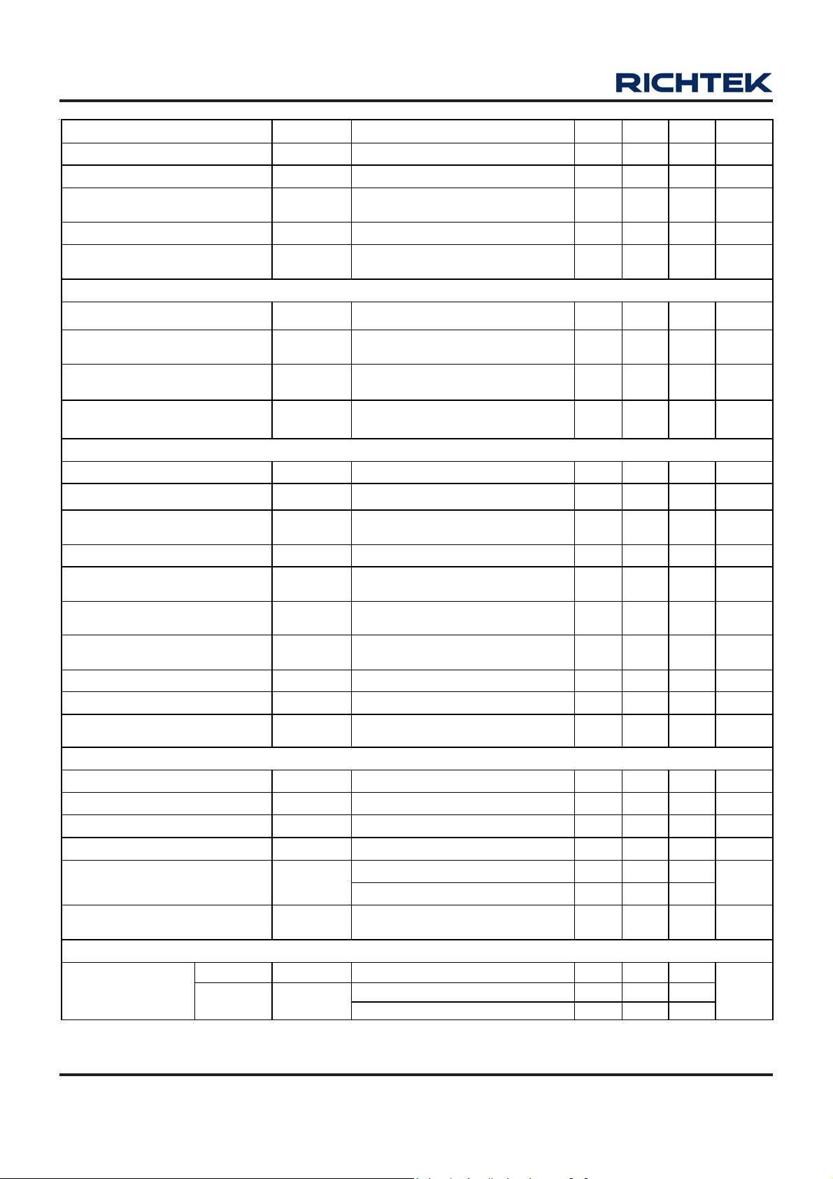
Electrical Characteristics
(VDD = V
PWM Controller
Quiescent Current IQ
TON Operating Current -- 15 -- μA
Shutdown Current I
FB Reference Voltage VFB V
= 5V, VIN = 15V, V
DDP
EN/DEM
= VDD, R
= 1MΩ, T
TON
= 25°C, unless otherwise specified)
A
Parameter Symbol Test Conditions Min Typ Max Unit
V
SHDN
+ V
DD
the regulati on point
VDD + V
TON -- 1 5
V
EN/DEM
= 4.5V to 5.5V 0.742 0.75 0.758 V
DD
, VFB = 0.8 V, forced abo ve
DDP
-- 1 10
DDP
-- -- 1250 μA
μA
= 0V −10 −1 --
To be continued
DS8204L-04 April 2011 www.richtek.com
5
RT8204L
Parameter Symbol Test Conditions Min Typ Max Unit
FB Input Bias Current VFB = 0.75V −1 0.1 1 μA
Output Voltage Range V
On-Time
Minimum Off-Time 250 400 550 ns
VOUT Shutdown Discharge
Resistance
Current Sensing
Current Limit Source Current LGATE = High 18 20 22 μA
0.75 -- 3.3 V
OUT
= 15V, V
V
IN
R
TON
= 1MΩ
= 1.25V,
OUT
267 334 401 ns
EN/DEM = GND -- 20 -- Ω
Current Limiter Temperature
Coefficient
Current Comparator Offset
Voltage
Zero Crossing Threshold
Voltage
TC
On the basis of 25°C -- 4700 -- ppm/°C
ICS
GND to OC −10 -- 10 mV
PHASE to GND, V
EN/ DEM
= 5V −10 -- 5 mV
Fault Pr otection
Current Limit Sense Voltage GND − PHASE, R
Output Under Voltage Threshold V
Over Voltage Protection
Threshold
60 70 80 %
UVP
V
OVP
With respect to error comparator
threshold
= 10kΩ 170 200 230 mV
ILIM
110 115 120 %
Over Voltage Fault Delay FB forced above OV threshold -- 20 -- μs
Under Voltage Lockout
Threshold
Under Voltage Lockout
Hysteresis
-- 150 -- mV
Soft-Start Ramp Time tSS
Falling edge, PWM disabled below
this level
From EN high to internal V
REF
reaches 0.71V (0Æ95%)
3.7 3.9 4.1 V
-- 1.5 -- ms
Under Voltage Blank Time From EN signal going high -- 4.5 -- ms
Thermal Shutdown T
Thermal Shutdown Hysteresis ΔT
SD_PWM
-- 155 -- °C
SD_PWM
-- 10 -- °C
Driver On-Resistance
UGATE Driver Source R
UGATE Driver Sink R
LGATE Driver Source R
LGATE Driver Sink R
Dead Time
Internal BOOT Charging Switch
On Resistance
Logic I/O
EN/DEM Input
Threshold Voltage
Logic-Low VIL EN/DEM Low -- -- 0.8
Logic-High V
6
UGATEsr
UGATEsk
LGATE sr
LGATE sk
BOOT to PHASE forced to 5V -- 2 -- Ω
BOOT to PHASE forced to 5V -- 1.5 -- Ω
LGATE, High State -- 1.5 -- Ω
LGATE, Low State -- 0.7 -- Ω
LGATE Rising (V
UGATE Rising -- 30 --
= 1.5V) -- 30 --
PHASE
ns
VDDP to BOOT, 10mA -- -- 90 Ω
IH
EN/DEM High 2.9 -- -EN/DEM Float -- 2 --
V
To be continued
DS8204L-04 April 2011www.richtek.com

RT8204L
Parameter Symbol Test Conditions Min Typ Max Unit
Logic Input Current
PGOOD (upper side thresh old decide by OV threshold)
Trip Threshold (falling)
Fault Propagation Delay
Output Low Voltage I
Leakage Current High state, forced to 5V -- -- 1 μA
LDO Controller
Quiescent Current I
LEN Threshold
Voltage
Logic-High V
Logic-Low V
LEN Input Current I
LFB Reference Voltage V
LFB Input Current I
LDRV Output Current I
Soft-Start Time V
Output Under Voltage
Protection Threshold
LDO Under Voltage
Blanking Time
Power Good Threshold
(falling)
LDO Power Good
Propagation Delay
LPGOOD Low Voltage I
Leakage Current High state, forced to 5V -- -- 1 μA
Thermal shutdown T
Thermal shutdown
Hysteresis
EN/DEM = VDD -- 1 10
μA
EN/DEM = 0 −10 1 --
Measured at FB, with respect to
reference, no load. Hysteresis = 3%
Falling edge, FB forced below
PGOOD trip threshold
= 1mA -- -- 0.4 V
SINK
PWM Off, LDO On, I
Q_LDO
1.2 -- --
IH_LDO
-- -- 0.8
IL_LDO
V
IN_LEN
REF_LFB
IN_LFB
OUT_LDRV
0.739 0.75 0.761 V
−1 -- 1 μA
= 5V, (internal pull low) -- -- 10 μA
LEN
Sourcing, LFB = 0.72 1.4 2 --
Sinking, LFB = 0.78 1.4 2 --
= 0.75V -- 2 -- ms
LFB
= 0A -- -- 400 μA
LOA D
87 90 93 %
-- 2.5 -- μs
V
mA
Measured at LFB pin 40 50 60 %
-- 4 -- ms
Measured at LFB pin 87 90 93 %
SD _LDO
ΔT
SD_LDO
Falling edge, LFB forced below
LPGOOD trip threshold
= 1mA -- -- 0.4 V
SINK
-- 2.5 -- μs
Hysteresis = 10°C -- 155 -- °C
-- 10 -- °C
Note 1. Stresses listed as the above “Absolute Maximum Ratings” may cause permanent damage to the device. These are for
stress ratings. Functional operation of the device at these or any other conditions beyond those indicated in the
operational sections of the specifications is not implied. Exposure to absolute maximum rating conditions for extended
periods may remain possibility to affect device reliability.
Note 2. θ
Note 3. Devices are ESD sensitive. Handling precaution is recommended.
Note 4. The device is not guaranteed to function outside its operating conditions.
DS8204L-04 April 2011 www.richtek.com
is measured in natural convection at T
JA
JEDEC 51-7 thermal measurement standard. The measurement case position of θ
package.
= 25°C on a high-effective thermal conductivity four- layer test board of
A
is on the exposed pad of the
JC
7

RT8204L
Typical Operating Characteristics
V
Efficiency vs. Output Current
100
Efficiency (%)
OUT1
90
80
70
60
50
40
30
20
10
0
0.001 0.01 0.1 1 10 100
DEM
PWM
VIN = 8V, V
OUT1
Output Current (A)
V
Efficiency vs. Output Current
OUT1
DEM
PWM
0
VIN = 12V, V
0.001 0.01 0.1 1 10 100
OUT1
Efficiency (%)
100
90
80
70
60
50
40
30
20
10
Output Current (A)
= 1.05V
= 1.05V
Switching Frequency vs. Output Current
350
325
300
275
250
225
200
175
150
125
100
75
Switching Frequency (kHz) 1
50
25
0
0.001 0.01 0.1 1 10 100
PWM
DEM
VIN = 8V, V
OUT1
Output Current (A)
Switching Frequency vs . Output Current
350
325
300
275
250
225
200
175
150
125
100
75
Switching Frequency (kHz) 1
50
25
0
0.001 0.01 0.1 1 10 100
PWM
DEM
VIN = 12V, V
Output Current (A)
OUT1
= 1.05V
= 1.05V
V
Efficiency vs. Output Current
OUT1
100
90
80
70
60
50
40
Efficiency (%)
30
20
10
0
0.001 0.01 0.1 1 10 100
DEM
PWM
VIN = 20V, V
OUT1
= 1.05V
Output Current (A)
Switching Frequency vs. Output Current
350
325
300
275
250
225
200
175
150
125
100
75
Switching Frequency (kHz) 1
50
25
0
0.001 0.01 0.1 1 10 100
PWM
DEM
VIN = 20V, V
Output Current (A)
OUT1
= 1.05V
DS8204L-04 April 2011www.richtek.com
8

RT8204L
1.0640
1.0632
1.0624
1.0616
Output Voltage (V)
1.0608
1.0600
LDO Output Voltage vs. Output Current
V
= 1.5V
IN_LDO
012345
Output Current (A)
Shutdown Current vs. Input Voltage
10
8
520
500
480
460
440
Standby Current (µA) 1
420
400
V
OUT1
(1V/Div)
Standby Current v s . Input Voltage
V
= 5V, No Load
EN/DEM
7 101316192225
Input Voltage (V)
Power On from EN_PWM Mode
6
4
Shutdown Current (µA) 1
2
0
V
OUT1
(1V/Div)
V
PHASE
(10V/Div)
V
EN/DEM
(5V/Div)
V
PGOOD
(5V/Div)
EN/DEM = GND, No Load
7 1013161922 25
Input Voltage (V)
Power On from EN_DEM Mode
VIN = 12V, V
EN_DEM
= 5V, No Load
V
PHASE
(10V/Div)
V
EN/DEM
(2V/Div)
V
PGOOD
(5V/Div)
V
OUT1
(1V/Div)
V
EN/DEM
(2V/Div)
V
UGATE
(20V/Div)
V
LGATE
(5V/Div)
VIN = 12V, EN/DEM = Floating, No Load
Time (1ms/Div)
Power Off from EN
VIN = 12V, EN/DEM = Floating, No Load
Time (1ms/Div)
Time (10ms/Div)
DS8204L-04 April 2011 www.richtek.com
9
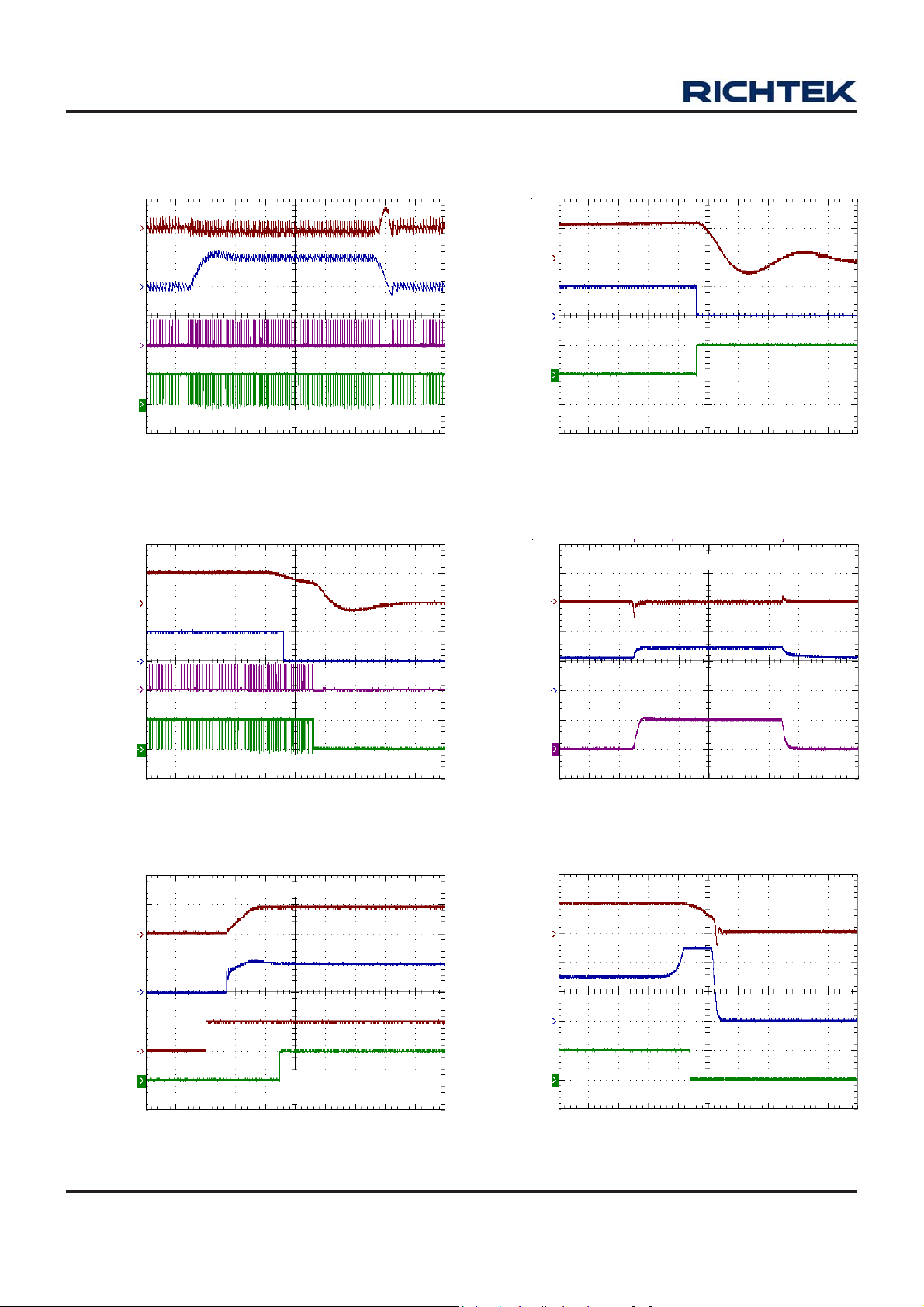
RT8204L
V
OUT1
V
OUT1
(50mV/Div)
I
L
(20A/Div)
V
UGATE
(20V/Div)
V
LGATE
(5V/Div)
VIN = 12V, EN/DEM = Floating, I
Load Transient Response
= 0A to 20A
OUT1
V
OUT1
(1V/Div)
V
PGOOD
(5V/Div)
V
LGATE
(5V/Div)
Over Voltage Protection
VIN = 12V, V
= 5V, No Load
EN/DEM
V
OUT1
(1V/Div)
V
PGOOD
(5V/Div)
V
UGATE
(20V/Div)
V
LGATE
(5V/Div)
Time (40μs/Div)
Under Voltage Protection
VIN = 12V, EN/DEM = Floating, No Load
Time (40μs/Div)
LDO Power On from LEN
No Load on OUT_PWM and OUT_LDO
V
OUT2
(100mV/Div)
V
LDRV
(2V/Div)
I
LOAD
(5A/Div)
Time (40μs/Div)
LDO Load Transient Response
V
IN_LDO
= 1.5V, C
= 10μF x2, I
OUT
OUT2
= 0A to 5A
Time (100μs/Div)
LDO Short-Circuit Protection
V
10
V
OUT2
(1V/Div)
V
LDRV
(2V/Div)
V
LEN
(5V/Div)
LPGOOD
(5V/Div)
VIN = 12V, V
CIN = 10μF, C
Time (2ms/Div)
IN_LDO
= 10μF x 2
OUT
= 1.5V
V
OUT2
(1V/Div)
V
LDRV
(2V/Div)
V
LPGOOD
(5V/Div)
V
IN_LDO
= 1.5V, C
= 10μF x 2, V
OUT
Time (100μs/Div)
DS8204L-04 April 2011www.richtek.com
OUT2
Short

Applications Information
RT8204L
The RT8204L PWM controller provides the high efficiency,
excellent transient response, and high DC output accuracy
needed for stepping down high voltage batteries to
generate low voltage CPU core, I/O, and chipset RAM
supplies in notebook computers. RichTek's Mach
ResponseTM technology is specifically designed for
providing 100ns “instant-on” response to load steps while
maintaining a relatively constant operating frequency and
inductor operating point over a wide range of input voltages.
The topology circumvents the poor load transient timing
problems of fixed frequency current mode PWMs while
also avoiding the problems caused by widely varying
switching frequencies in conventional constant-on-time and
constant- off-time PWM schemes. The DRVTM mode PWM
modulator is specifically designed to have better noise
immunity for such a single output application.
PWM Operation
The Mach Response
TM
DRVTM mode controller relies on
,
the output filter capacitor's effective series resistance
(ESR) to act as a current-sense resistor, so the output
ripple voltage provides the PWM ramp signal. Referring to
the function diagrams of the RT8204L, the synchronous
high side MOSFET is turned on at the beginning of each
cycle. After the internal one shot timer expires, the
MOSFET is turned off. The pulse width of this one shot is
determined by the converter’s input and output voltages
to keep the frequency fairly constant over the input voltage
range. Another one-shot sets a minimum off-time (400ns
typ.).
On-Time Control (TON)
The on-time one-shot comparator has two inputs. One
input looks at the output voltage, while the other input
samples the input voltage and converts it to a current.
This input voltage proportional current is used to charge
an internal on-time capacitor. The on-time is the time
required for the voltage on this capacitor to charge from
zero volts to V
, thereby making the on-time of the high
OUT
side switch directly proportional to the output voltage and
inversely proportional to the input voltage. The
implementation results in a nearly constant switching
frequency without the need of a clock generator.
3.85p x R x V
t =
ON
TON OUT
(V 0.5)−
IN
And then the switching frequency is :
V
Frequency =
R
is a resistor connected from the input supply (VIN)
TON
OUT
(V x t
IN ON
)
to the TON pin.
Mode Selection (EN/DEM) Operation
The EN/DEM pin enables the supply. When EN/DEM is
tied to VDD, the controller is enabled and operates in
diode-emulation mode. When the EN/DEM pin is floating,
the RT8204L will operate in forced-CCM mode.
Diode-Emulation Mode (EN/DEM = High)
In diode-emulation mode, the RT8204L automatically
reduces switching frequency at light load conditions to
maintain high efficiency. This reduction of frequency is
achieved smoothly and without increasing VOUT ripple or
load regulation. As the output current decreases from
heavy-load condition, the inductor current is also reduced,
and eventually comes to the point when its valley touches
zero current, which is the boundary between continuous
conduction and discontinuous conduction modes. By
emulating the behavior of diodes, the low side MOSFET
allows only partial negative current when the inductor
freewheeling current becomes negative. As the load current
is further decreased, it takes longer and longer to discharge
the output capacitor to the level that requires the next
“ON” cycle. The on-time is kept the same as that in the
heavy-load condition. In reverse, when the output current
increases from light load to heavy load, the switching
frequency increases to the preset value as the inductor
current reaches the continuous condition. The transition
load point to the light load operation can be calculated as
follows (Figure 1) :
(V V )
−
I x t
LOAD ON
≈
IN OUT
2L
where tON is the On-time.
DS8204L-04 April 2011 www.richtek.com
11

RT8204L
I
L
Slope = (VIN -V
0
t
ON
OUT
) / L
I
L, PEAK
I
LOAD
t
= I
L, PEAK
/ 2
Figure 1. Boundary Condition of CCM/DEM
The switching waveforms may appear noisy and
asynchronous when light loading causes diode-emulation
operation, however, this is a normal operating condition
that results in high light load efficiency. Trade-offs in DEM
noise vs. light load efficiency are made by varying the
inductor value. Generally, low inductor values produce a
broader efficiency vs. load curve, while higher values result
in higher full-load efficiency (assuming that the coil
resistance remains fixed) and less output voltage ripple.
The disadvantages for using higher inductor values include
larger physical size and degraded load-transient response
(especially at low input voltage levels).
I
L
I
L, PEAK
I
LOAD
I
LIM
0
t
Figure 2. Valley Current Limit
Current sensing of the RT8204L can be accomplished in
two ways. Users can either use a current-sense resistor
or the on-state of the low side MOSFET (R
DS(ON)
). For
resistor sensing, a sense resistor is placed between the
source of low side MOSFET and PGND (Figure 3(a)).
R
sensing is more efficient and less expensive (Figure
DS(ON)
3(b)). However, there is a compromise between current
limit accuracy and sense resistor power dissipation.
PHASE
LGATE
Forced-CCM Mode (EN/DEM = floating)
The low noise, forced-CCM mode (EN/DEM = floating)
disables the zero crossing comparator, which controls
the low side switch on-time. This causes the low side
gate-drive waveform to become the complement of the
high-side gate-drive waveform. This in turn causes the
inductor current to reverse at light loads as the PWM loop
to maintain a duty ratio V
OUT/VIN
. The benefit of forced-
CCM mode is to keep the switching frequency fairly
constant, but it comes at a cost. The no-load battery
current can be as high as 10mA to 40mA, depending on
the external MOSFETs.
Current Limit Setting (OCP)
The RT8204L has a cycle-by-cycle current limiting control.
The current limit circuit employs a unique“valley” current
sensing algorithm. If the magnitude of the current-sense
signal at OC is above the current-limit threshold, the PWM
is not allowed to initiate a new cycle (Figure 2).
OC
R
ILIM
(a)
PHASE
LGATE
OC
R
ILIM
(b)
Figure 3. Current Sense Methods
In both cases, the R
resistor between the OC pin and
ILIM
PHASE pin sets the over current threshold. This resistor
R
is connected to a 20μA current source within the
ILIM
RT8204L which is turned on when the low side MOSFET
turns on. When the voltage drop across the sense resistor
or low side MOSFET equals the voltage across the R
ILIM
resistor, positive current limit will activate. The high side
12
DS8204L-04 April 2011www.richtek.com

MOSFET will not be turned on until the voltage drop across
the sense element (resistor or MOSFET) falls below the
voltage across the R
resistor.
ILIM
Choose a current limit resistor by the following equation :
I x R
R =
ILIM
LIMIT SENSE
20μA
Carefully observe the PC board layout guidelines to ensure
that noise and DC errors do not corrupt the current sense
signal seen by OC and PGND. Mount the IC close to the
low-side MOSFET and sense resistor with short, direct
traces, making a Kelvin sense connection to the sense
resistor.
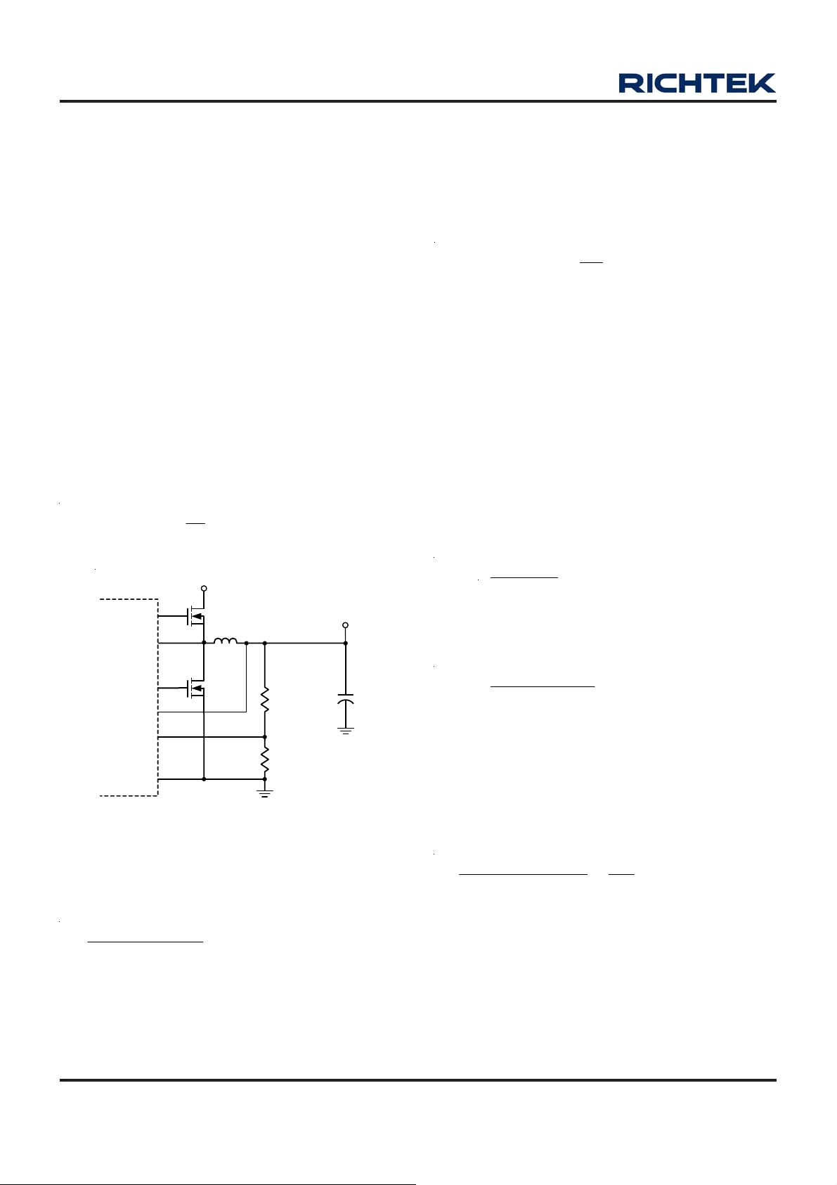
MOSFET Gate Driver (UGATE, LGA TE)
The high side driver is designed to drive high current, low
R
N-MOSFET(s). When configured as a floating driver,
DS(ON)
5V bias voltage is delivered from VDDP supply. The average
drive current is proportional to the gate charge at VGS =
5V times the switching frequency. The instantaneous drive
current is supplied by the flying capacitor between BOOT
and PHASE pins.
A dead time to prevent shoot through is internally
generated between high side MOSFET off to low side
MOSFET on, and low side MOSFET off to high side
MOSFET on.
The low side driver is designed to drive high current, low
R
N-MOSFET(s). The internal pull down transistor
DS(ON)
that drives LGATE low is robust, with a 0.6Ω typical on
resistance. A 5V bias voltage is delivered form VDDP
supply. The instantaneous drive current is supplied by the
flying capacitor between VDDP and PGND.
For high current applications, some combinations of high
and low side MOSFETs might be encountered that will
cause excessive gate-drain coupling, which can lead to
efficiency-killing, EMI producing shoot through currents.
This is often remedied by adding a resistor in series with
BOOT, which increases the turn-on time of the high side
MOSFET without degrading the turn-off time (Figure 4).
RT8204L
V
+5V
BOOT
UGATE
PHASE
R
Figure 4. Reducing the UGATE Rise Time
Power Good Output (PGOOD)
The power good output is an open-drain output and requires
a pull up resistor. When the output voltage is 15% above
or 10% below its set voltage, PGOOD gets pulled low. It
is held low until the output voltage returns to within these
tolerances once more. In soft start, PGOOD is actively
held low and is allowed to transition high until soft start is
over and the output reaches 93% of its set voltage. There
is a 2.5μs delay built into PGOOD circuitry to prevent
false transition.
POR, UVLO and Soft-Start
Power on reset (POR) occurs when VDD rises above to
approximately 4.1V. The RT8204L will reset the fault latch
and prepare the PWM for operation. At below 3.7V (min),
the VDD under voltage lockout (UVLO) circuitry inhibits
switching by keeping UGATE and LGATE low.
A built in soft-start is used to prevent surge current from
power supply input after EN/DEM is enabled. It clamps
the ramping of internal reference voltage which is compared
with the FB signal. The typical soft-start duration is 1.5ms.
Output Over Voltage Protection (OVP)
The output voltage can be continuously monitored for over
voltage protection. When the output voltage exceeds 15%
of its set voltage threshold, over voltage protection is
triggered and the low side MOSFET is latched on. This
activates the low side MOSFET to discharge the output
capacitor.
IN
The RT8204L is latched once OVP is triggered and can
only be released by VDD or EN/DEM power-on reset. There
is a 20μs delay built into the over voltage protection circuit
to prevent false transitions.
DS8204L-04 April 2011 www.richtek.com
13
RT8204L
Output Under Voltage Protection (UVP)
The output voltage can be continuously monitored for under
voltage protection. When the output voltage is less than
70% of its set voltage threshold, under voltage protection
is triggered and then both UGATE and LGATE gate drivers
are forced low. In order to remove the residual charge on
the output capacitor during the under voltage period, if
PHASE is greater than 1V, the LGATE is forced high until
PHASE is lower than 1V. There is 2.5μs delay built into
the under voltage protection circuit to prevent false
transitions. During soft-start, the UVP will be blanked
around 4.5ms.
Output V oltage Setting (FB)
The output voltage can be adjusted from 0.75V to 3.3V by
setting the feedback resistors R7 and R8 (Figure 5).
Choose R8 to be approximately 10kΩ, and solve for R7
using the equation :
R7
V = V x 1 +
OUT FB
⎛⎞
⎜⎟
R8
⎝⎠
where VFB is 0.75V.
V
IN
UGATE
PHASE
LGATE
R7
VOUT
FB
R8
GND
V
OUT
Find a low pass inductor having the lowest possible DC
resistance that fits in the allowed dimensions. Ferrite cores
are often the best choice, although powdered iron is
inexpensive and can work well at 200kHz. The core must
be large enough not to saturate at the peak inductor current
(I
) :
PEAK
LIR
I = I + x I
PEAK LOAD(MAX) LOAD(MAX)
⎛⎞
⎜⎟
2
⎝⎠
Output Capacitor Selection
The output filter capacitor must have ESR low enough to
meet output ripple and load transient requirement, yet have
high enough ESR to satisfy stability requirements. Also,
the capacitance value must be high enough to absorb the
inductor energy going from a full load to no load condition
without tripping the OVP circuit.
For CPU core voltage converters and other applications
where the output is subject to violent load transient, the
output capacitor's size depends on how much ESR is
needed to prevent the output from dipping too low under a
load transient. Ignoring the sag due to finite capacitance :
V
P P
ESR
≤
−
I
LOAD(MAX)
In non-CPU applications, the output capacitor's size
depends on how much ESR is needed to maintain at an
acceptable level of output voltage ripple :
V
P P
ESR
≤
LIR x I
−
LOAD(MAX)
Organic semiconductor capacitor(s) or special polymer
capacitor(s) are recommended.
Output Capacitor Stability
Figure 5. Setting The Output Voltage
Output Inductor Selection
The switching frequency (on-time) and operating point
(% ripple or LIR) determine the inductor value as follows :
t x (V V )
ON IN OUT
L =
LIR x I
14
−
LOAD(MAX)
Stability is determined by the value of the ESR zero relative
to the switching frequency. The point of instability is given
by the following equation :
f = <
2 x x ESR x C 4
1
π
OUT
f
SW
Do not put high value ceramic capacitors directly across
the outputs without taking precautions to ensure stability.
Large ceramic capacitors can have a high-ESR zero
frequency and cause erratic and unstable operation.
However, it is easy to add sufficient series resistance by
placing the capacitors a couple of inches downstream from
the inductor and connecting VOUT or the FB divider close
to the inductor.
DS8204L-04 April 2011www.richtek.com

RT8204L
There are two related but distinct ways, double pulsing
and feedback loop instability to identify the unstable
operation.
Double pulsing occurs due to noise on the output or
because the ESR is too low such that there is not enough
voltage ramp in the output voltage signal. This“fools” the
error comparator into triggering a new cycle immediately
after the 400ns minimum off-time period has expired.
Double pulsing is more annoying than harmful, resulting
in nothing worse than increased output ripple. However, it
may indicate the possible presence of loop instability,
which is caused by insufficient ESR.
Loop instability can result in oscillation at the output after
line or load perturbations and trip the over voltage
protection latch or cause the output voltage to fall below
the tolerance limit.
The easiest method for stability checking is to apply a
very zero-to-max load transient and carefully observe the
output-voltage-ripple envelope for overshoot and ringing. It
helps to simultaneously monitor the inductor current with
an AC probe. Do not allow more than one ringing cycle
after the initial step response under shoot or over shoot.
LDO Normal Operation
The RT8204L LDO controls an N-MOSFET to produce a
tightly regulated output voltage from higher supply voltage.
It takes 5V power supply for controller and draws maximally
400μA while operating.
The feedback voltage is regulated to compare with the
internal 0.75V reference voltage. To set the output voltage,
feedback the conjunction of a resistive voltage divider from
output node to ground for the LFB pin.
Depending upon the input voltage used for the device, the
LDRV pin can pull up near to VDD. Thus, the device can
be used to regulate a large range of output voltage by
careful selection of the external MOSFETs.
The RT8204L LDO includes an active high enable control
(LEN pin) used to turn on RT8204L LDO. If this pin is
pulled low, the LDRV pin is pulled low, turning off the
N-MOSFET. If this pin is pulled higher than 1.2V, the LDRV
pin is enabled.
The RT8204L LDO contains a power good output pin
(LPGOOD pin), which is an open drain output that pulled
low if the output is below the power good threshold
(typically 90% of the programmed output voltage, or 93%
at start up). The power good detection is active if the
RT8204L LDO is enabled.
Also included is an under voltage protection circuit that
monitors the output voltage. If the output voltage drops
below 50% (typical) of nominal, as would occur during
over current or short condition, the RT8204L LDO will pull
the LDRV pin low and latch off. The RT8204L LDO is
latched once UVP is triggered and can only be relieved
by VDD or LEN power on reset.
LDO Driver and Stability Design
The drive output (LDRV pin) is sink/source capable. The
sink current is typically 2mA, while the source current is
typically 2mA in normal operation.
The drive output is also used for stabilizing the loop of the
system using different types of output capacitors. The
components listed in the table below are used.
Table 1. LDO Configuration and Compensation
LDO Configuration Compensator
Input
Voltage
1.25V 1.05V 33nF 39pF 82Ω
1.5V 1.05V 33nF 47pF 43Ω
1.5V 1.25V 33nF 47pF 30Ω
1.8V 1.5V 33nF 39pF 100Ω
Note : test condition is output capacitor 220μF (ESR : 9 to
25mΩ) or 100μF (ESR : 9 to 15mΩ) +MLCC 10μF output
current is from 0.1A to 5A
Outpu t
Voltage
C9 C10 R9
LDO Output V oltage Protection(UVP)
The RT8204L LDO has output under voltage protection
that monitors at the output to check if RT8204L :
(a) LDO output voltage is less than 50% (typical) of its
nominal value and
(b) V
is within 900mV (typical) of its maximum.
LDRV
This provides inherent immunity to under voltage shut down
at start up since V
has a slow rate of rising at this
LDRV
moment. If both of these criteria are met, the output is
shut down by means of pulling V
to ground
LDRV
immediately.
DS8204L-04 April 2011 www.richtek.com
15

RT8204L
If the VDDP input is supplied prior to the LDO_VIN, it
could accidentally meet the UVP fault protection. To avoid
entering UVP latch off, use the enable control (LEN pin)
VDDP
VTH(UV) = 0.88V
LDO_VIN
VTH(LEN) = 1.2V
LEN
RT8204L Supply Comes Up Before MOSFET Drain Supply
VDDP
VTH(UV) = 0.88V
LDO_VIN
to turn the system on after all power supplies are ready.
Refer to the power sequencing example below (Figure 6).
VTH(LEN) occurs after VTH(UV) is reached
VTH(LEN) = 1.2V
LEN
MOSFET Drain Supply Comes Up Before RT8204L Supply
Figure 6. Power Supply Sequencing
LDO Output Voltage Setting
The LFB pin connects directly to the inverting input of the
error amplifier, and the output voltage is set using external
resistors R11 and R12 (Figure 7). The following equation
is for adjusting the output voltage :
R11
V = V x 1 +
OUT LFB
where V
LFB
⎛⎞
⎜⎟
R12
⎝⎠
is 0.75V (typ.).
LDO Output Capacitor Selection
Low ESR capacitors such as Sanyo POSCAPs or
Panasonic SP-caps are recommended for bulk
capacitance, and ceramic bypass capacitors are
recommended for decoupling high frequency transients.
VTH(LEN) occurs after VTH(UV) is reached
LEN rising with VDDP shown
LDO Input Capacitor Selection
Low ESR capacitors such as Sanyo POSCAPs or
Panasonic SP-caps are recommended for the input
capacitors to provide better load transient response. If the
LDO input is connected from the output of buck converter
(V
), a 0.1μF ceramic capacitor will be sufficient.
OUT1
LDO_VIN (V
LDRV
R11
LFB
R12
)
OUT1
LDO_VOUT (V
OUT2
)
16
Figure 7. LDO Output Voltage Setting
DS8204L-04 April 2011www.richtek.com

RT8204L
LDO MOSFET Selection
1.60
1.40
Four-Layer PCB
Low threshold N-MOSFETs are required. For the device
to work under all operating conditions, a maximum R
DS(ON)
must be met to ensure that the output will not go into
dropout :
VV
R = ( )
DS(ON)(MAX)
Note that R
DS(ON)
IN(MIN) OUT(MAX)
must be met for operating temperature
−
I
OUT(PEAK)
Ω
range at the minimum VGS condition.
Power consumptions of the N-MOSFETs should be taken
into consideration for the selection of various package
types.
Thermal Considerations
For continuous operation, do not exceed absolute
maximum junction temperature. The maximum power
dissipation depends on the thermal resistance of the IC
package, PCB layout, rate of surrounding airflow, and
difference between junction and ambient temperature. The
1.20
1.00
0.80
0.60
0.40
0.20
Maximum Power Dissipation (W) 1
0.00
0 25 50 75 100 125
Ambient Temperature (°C)
Figure 8. Derating Curve for the RT8204L Package
Layout Consideration
Layout is very important in high frequency switching
converter design. If designed improperly, the PCB could
radiate excessive noise and contribute to converter
instability. Certain points must be considered before
starting a layout for the RT8204L.
maximum power dissipation can be calculated by the
following formula :
` Connect RC low-pass filter from VDDP to VDD, 1μF and
20Ω are recommended. Place the filter capacitor close
P
where T
the ambient temperature, and θ
thermal resistance.
For recommended operating condition specifications of
the RT8204L, the maximum junction temperature is 125°C
and TA is the ambient temperature. The junction to ambient
D(MAX)
= (T
J(MAX)
− TA) /θ
J(MAX)
JA
is the maximum junction temperature, TA is
is the junction to ambient
JA
to the IC.
` Keep current limit setting network as close as possible
to the IC. Routing of the network should avoid coupling
to high-voltage switching node.
` Connections from the drivers to the respective gate of
the high side or low side MOSFET should be as short
as possible to reduce stray inductance.
thermal resistance, θJA, is layout dependent. For WQFN-
16L 3x3 packages, the thermal resistance, θJA, is 68°C/
W on a standard JEDEC 51-7 four-layer thermal test board.
The maximum power dissipation at TA = 25°C can be
calculated by the following formula :
` All sensitive analog traces and components such as
VOUT, FB, GND, EN/DEM, PGOOD, OC, VDD, and
TON should be placed away from high voltage switching
nodes such as PHASE, LGATE, UGATE, or BOOT
nodes to avoid coupling. Use internal layer(s) as ground
P
16L 3x3 package
The maximum power dissipation depends on the operating
ambient temperature for fixed T
resistance, θJA. For the RT8204L package, the derating
= (125°C − 25°C ) / (68°C/W) = 1.471W for WQFN-
D(MAX)
and thermal
J(MAX)
plane(s) and shield the feedback trace from power traces
and components.
` Current sense connections must always be made using
Kelvin connections to ensure an accurate signal, with
the current limit resistor located at the device.
curve in Figure 8 allows the designer to see the effect of
rising ambient temperature on the maximum power
dissipation.
` Power sections should connect directly to ground
plane(s) using multiple vias as required for current
handling (including the chip power ground connections).
Power components should be placed to minimize loops
and reduce losses.
DS8204L-04 April 2011 www.richtek.com
17

RT8204L
Outline Dimension
D
D2
L
SEE DETAIL A
1
E
e
A
A3
A1
E2
1
2
b
DETAIL A
1
2
Pin #1 ID and Tie Bar Mark Options
Note : The configuration of the Pin #1 identifier is optional,
but must be located within the zone indicated.
Dimensions In Millimeters Dimensions In Inches
Symbol
Min Max Min Max
A 0.700 0.800 0.028 0.031
A1 0.000 0.050 0.000 0.002
A3 0.175 0.250 0.007 0.010
b 0.180 0.300 0.007 0.012
D 2.950 3.050 0.116 0.120
D2 1.300 1.750 0.051 0.069
E 2.950 3.050 0.116 0.120
E2 1.300 1.750 0.051 0.069
e 0.500 0.020
L 0.350 0.450
Richtek Technology Corporation
Headquarter
5F, No. 20, Taiyuen Street, Chupei City
Hsinchu, Taiwan, R.O.C.
Tel: (8863)5526789 Fax: (8863)5526611
0.014 0.018
W-Type 16L QFN 3x3 Package
Richtek Technology Corporation
Taipei Office (Marketing)
5F, No. 95, Minchiuan Road, Hsintien City
Taipei County, Taiwan, R.O.C.
Tel: (8862)86672399 Fax: (8862)86672377
Email: marketing@richtek.com
Information that is provided by Richtek Technology Corporation is believed to be accurate and reliable. Richtek reserves the right to make any change in circuit
design, specification or other related things if necessary without notice at any time. No third party intellectual property infringement of the applications should be
guaranteed by users when integrating Richtek products into any application. No legal responsibility for any said applications is assumed by Richtek.
DS8204L-04 April 2011www.richtek.com
18

 Loading...