

®
RT8020
Dual High-Efficiency PWM Step-Down DC/DC Converter
General Description
The RT8020 is a dual high-efficiency Pulse-Width-
Modulated (PWM) step-down DC/DC converter. It is
capable of delivering 1A output current over a wide input
voltage range from 2.5V to 5.5V, the RT8020 is ideally
suited for portable electronic devices that are powered
from 1-cell Li-ion battery or from other power sources within
the range such as cellular phones, PDAs and other hand-
held devices.
Two operational modes are available : PWM/Low-Dropout
auto-switch and shutdown modes. Internal synchronous
rectifier with low R
loss at PWM mode. No external Schottky diode is
required in practical application.
The RT8020 enters Low-Dropout mode when normal PWM
cannot provide regulated output voltage by continuously
turning on the upper PMOS. The RT8020 enter shutdown
mode and consumes less than 0.1μA when EN pin is pulled
low.
dramatically reduces conduction
DS(ON)
Features
2.5V to 5.5V Input Range
Adjustable Output From 0.6V to V
1.2V, 1.3V, 1.8V, 2.5V and 3.3V Fixed/ Adjustable
IN
Output Voltage
1A Output Current
95% Efficiency
No Schottky Diode Required
50uA Quiescent Current per Channel
1.5MHz Fixed Frequency PWM Operation
Small 12-Lead WDFN Package
RoHS Compliant and 100% Lead (Pb)-Free
Applications
Mobile Phones
Personal Information Appliances
Wireless and DSL Modems
MP3 Players
Portable Instruments
The switching ripple is easily smoothed-out by small
package filtering elements due to a fixed operation
frequency of 1.5MHz. This along with small
WDFN-12L 3x3 package provides small PCB area
application. Other features include soft start, lower internal
reference voltage with 2% accuracy, over temperature
protection, and over current protection.
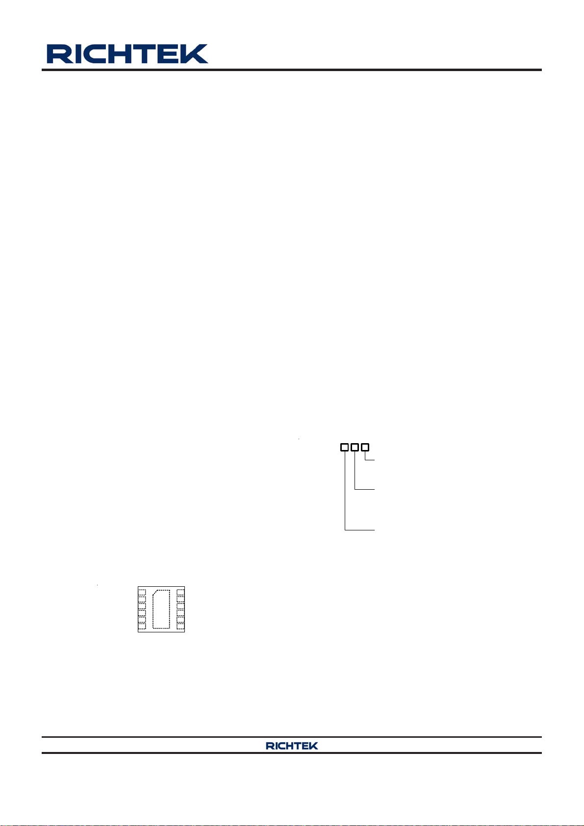
Pin Configurations
(TOP VIEW)
GND
12
EN2
11
NC2
10
FB2
9
GND
8
LX1
13
VIN1
1
VIN2
2
LX2
3
GND
4
FB1
5
NC1
67
EN1
WDFN-12L 3x3
Ordering Information
RT8020
Package Type
QW : WDFN-12L 3x3 (W-Type)
Lead Plating System
P : Pb Free
G : Green (Halogen Free and Pb Free)
Output Voltage : VOUT1/VOUT2
Default : Adjustable
A : 3.3V/1.8V
B : 3.3V/1.3V
C : 3.3V/1.2V
D : 2.5V/1.8V
Note :
Richtek products are :
` RoHS compliant and compatible with the current require-
ments of IPC/JEDEC J-STD-020.
` Suitable for use in SnPb or Pb-free soldering processes.
Copyright 2012 Richtek Technology Corporation. All rights reserved. is a registered trademark of Richtek Technology Corporation.
©
DS8020-06 March 2012 www.richtek.com
1
RT8020
(
)
Marking Information
RT8020APQW
C2- : Product Code
C2-YM
DNN
YMDNN : Date Code
RT8020CPQW
C4-YM
DNN
C4- : Product Code
YMDNN : Date Code
RT8020AGQW
C2=YM
DNN
RT8020BPQW
C3-YM
DNN
RT8020BGQW
C3=YM
DNN
C2= : Product Code
YMDNN : Date Code
C3- : Product Code
YMDNN : Date Code
C3= : Product Code
YMDNN : Date Code
RT8020CGQW
C4=YM
DNN
RT8020DPQW
C5-YM
DNN
RT8020DGQW
C5=YM
DNN
C4= : Product Code
YMDNN : Date Code
C5- : Product Code
YMDNN : Date Code
C5=: Product Code
YMDNN : Date Code
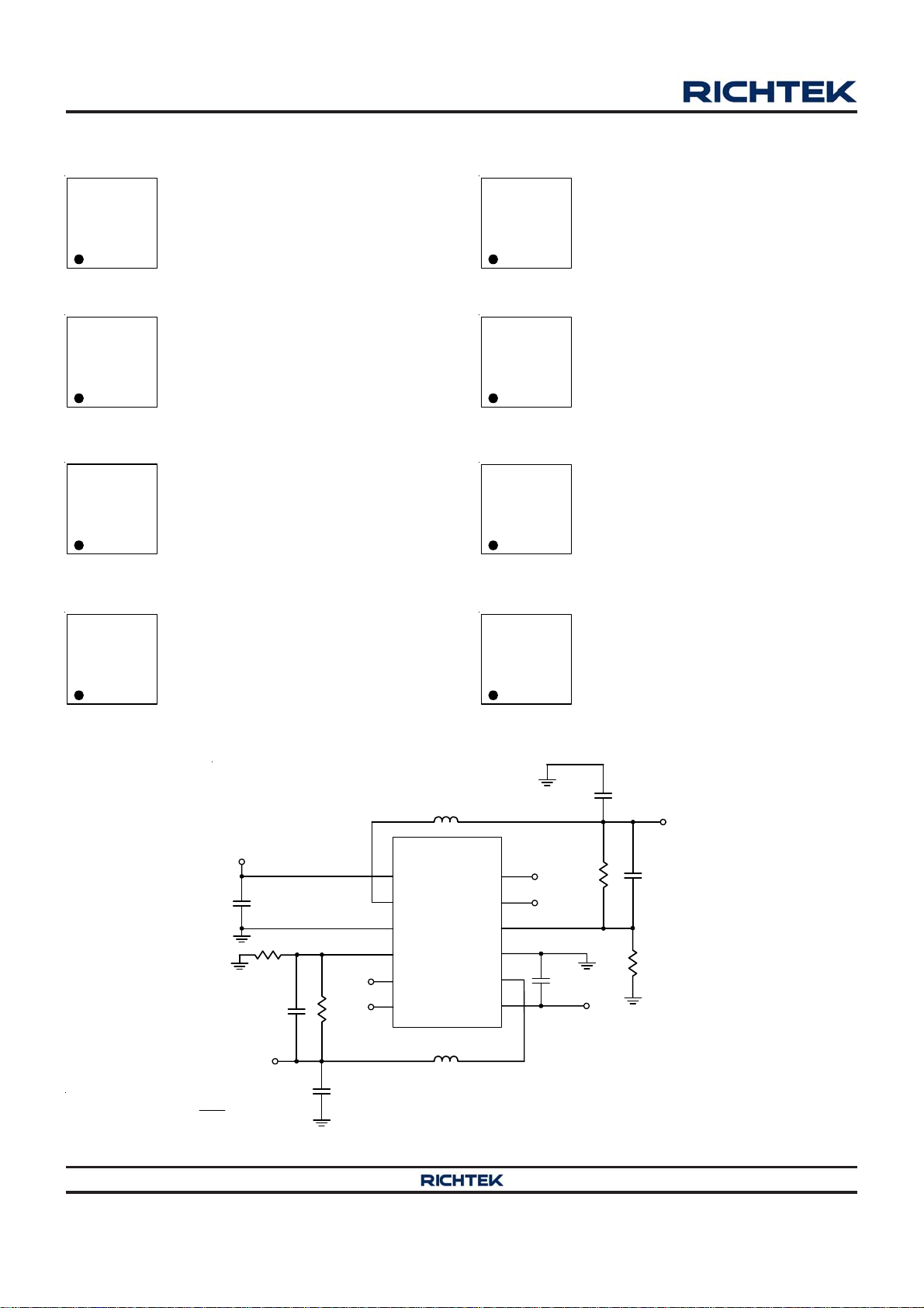
Typical Application Circuit
C
L2
2.2µH
V
IN2
C
IN2
4.7µF
3, Exposed Pad (13)
R12
C11
22pF
V
OUT1
Rx1
1 VV
REFOUTx
+×=
Rx2
R11
850k
C
OUT1
4.7µF
1
2
4
5
6
VIN2
LX2
GND
FB1
NC1
EN1
RT8020
L1
2.2µH
EN2
NC2
FB2
GND
LX1
VIN1
12
11
10
9
8
7
Figure 1. Adjustable Voltage Regulator
Copyright 2012 Richtek Technology Corporation. All rights reserved. is a registered trademark of Richtek Technology Corporation.
2
©
OUT2
4.7µF
R21
850k
C
IN1
4.7µF
V
OUT2
C21
22pF
R22
V
IN1
DS8020-06 March 2012www.richtek.com
V
= 1.2V, 1.3V, 1.8V, 2.5V or 3.3V
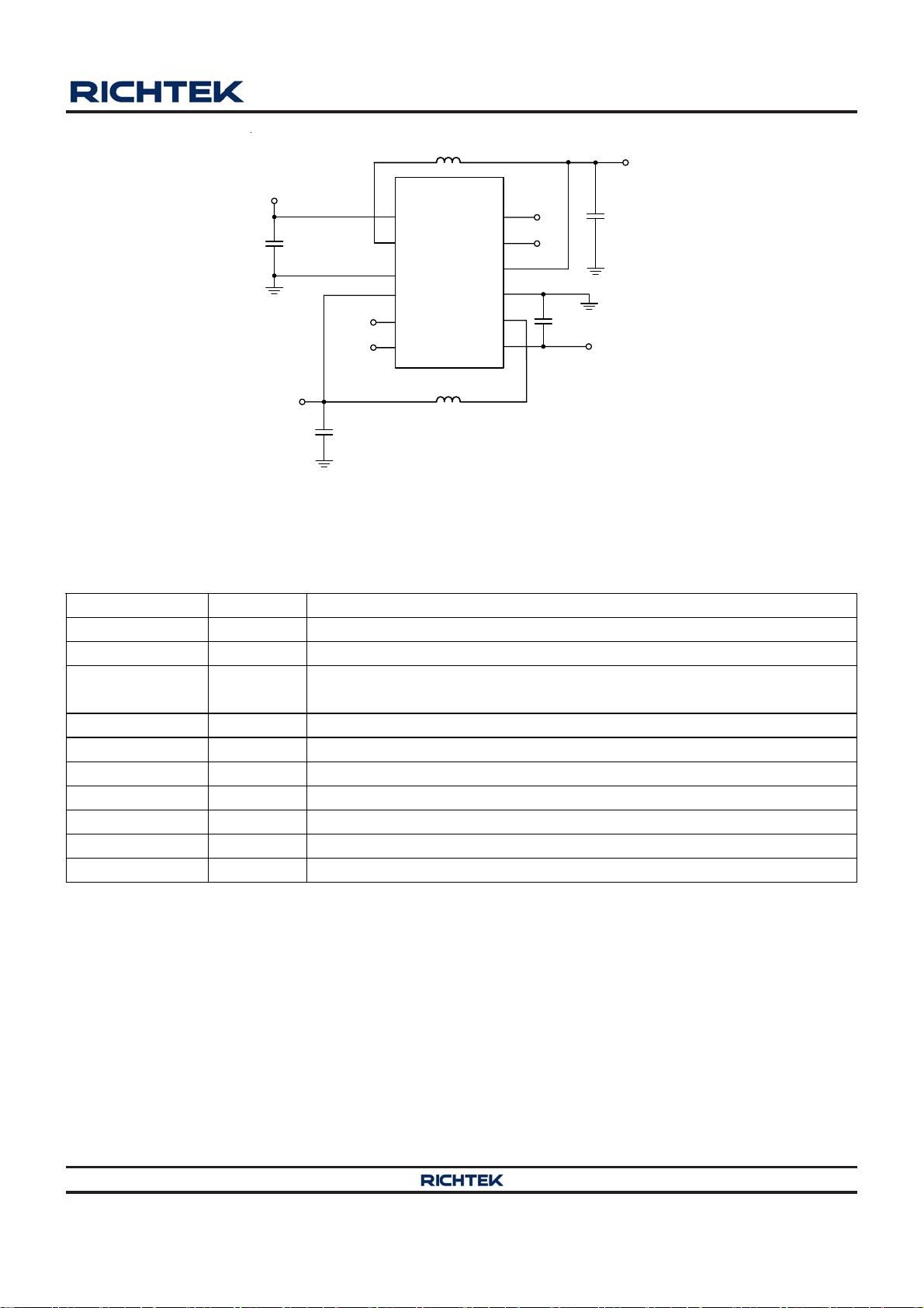
OUTx
V
IN2
C
IN2
4.7µF
3, Exposed Pad (13)
V
OUT1
C
4.7µF
L2
2.2µH
RT8020
OUT1
1
2
4
5
6
VIN2
LX2
GND
FB1
NC1
EN1
L1
2.2µH
EN2
NC2
FB2
GND
LX1
VIN1
12
11
10
9
8
7
Figure 2. Fixed Voltage Regulator
C
IN1
4.7µF
C
V
IN1
OUT2
4.7µF
V
RT8020
OUT2
Functional Pin Description
Pin No. Pin Name Pin Function
1 VIN2 Power Input of Channel 2.
2 LX2 Pin for Switching of Channel 2.
3, 9,
Exposed Pad (13)
4 FB1 Feedback of Channel 1.
5, 11 NC1, NC2 No Connection or Connect to VIN.
6 EN1 Chip Enable of Channel 1 (Active High). V
7 VIN1 Power Input of Channel 1.
8 LX1 Pin for Switching of Channel 1.
10 FB2 Feedback of Channel 2.
12 EN2 Chip Enable of Channel 2 (Active High). V
GND
Ground. The exposed pad must be soldered to a large PCB and connected to
GND for maximum power dissipation.
EN1
EN2
≦ V
≦ V
IN1.
IN2.
Copyright 2012 Richtek Technology Corporation. All rights reserved. is a registered trademark of Richtek Technology Corporation.
©
DS8020-06 March 2012 www.richtek.com
3
RT8020
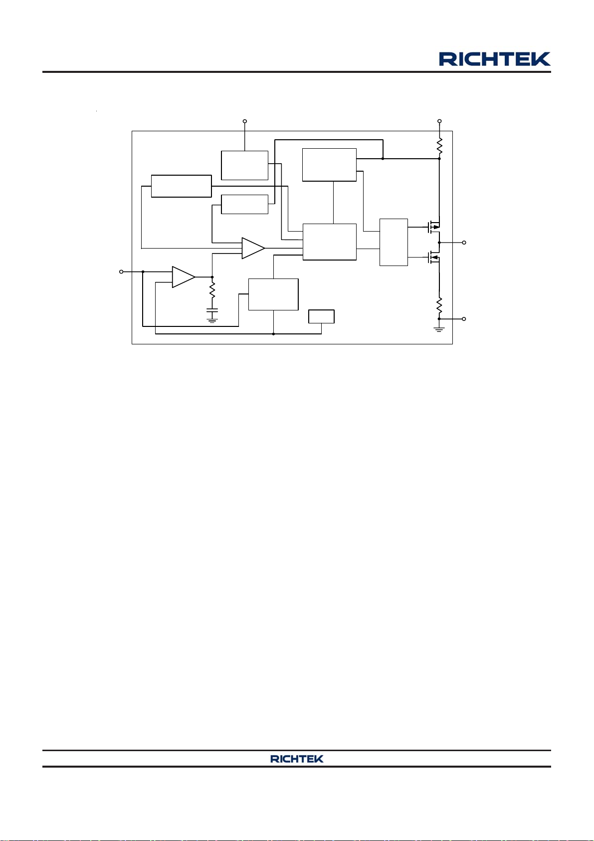
Function Block Diagram
ENx VINx
FBx
Slope
Compensation
Error
Amplifier
COMP
OSC and
Shutdown
Control
Current
Sense
PWM
Comparator
RC
UVLO and
Power Good
Detector
Current Limit
Detector
Control
Logic
V
REF
Driver
RS1
LXx
RS2
GND
Copyright 2012 Richtek Technology Corporation. All rights reserved. is a registered trademark of Richtek Technology Corporation.
©
DS8020-06 March 2012www.richtek.com
4
Absolute Maximum Ratings (Note 1)
RT8020
Supply Input Voltage, V
EN1, FB1, LX1, EN2, FB2 and LX2 Pin Voltage -------------------------------------------------------------- −0.3V to (V
Power Dissipation, P
, V
IN1
IN2
@ TA = 25°C
D
---------------------------------------------------------------------------------- −0.3V to 6.5V
IN
+ 0.3V)
WDFN-12L 3x3 -------------------------------------------------------------------------------------------------------- 1.667W
Package Thermal Resistance (Note 2)
WDFN-12L 3x3, θJA-------------------------------------------------------------------------------------------------- 60°C/W
WDFN-12L 3x3, θJC-------------------------------------------------------------------------------------------------- 8.2°C/W
Lead Temperature (Soldering, 10 sec.)-------------------------------------------------------------------------- 260°C
Junction Temperature ------------------------------------------------------------------------------------------------ 150°C
Storage Temperature Range --------------------------------------------------------------------------------------- −65°C to 150°C
ESD Susceptibility (Note 3)
HBM (Human Body Mode) ----------------------------------------------------------------------------------------- 2kV
MM (Machine Mode) ------------------------------------------------------------------------------------------------- 200V
Recommended Operating Conditions (Note 4)
Supply Input Voltage ------------------------------------------------------------------------------------------------- 2.5V to 5.5V
Junction Temperature Range ---------------------------------------------------------------------------------------
Ambient Temperature Range ---------------------------------------------------------------------------------------
−40°C to 125°C
−40°C to 85°C
Electrical Characteristics
(VIN = 3.6V, V
= 2.5V, V
OUT
= 0.6V, L = 2.2uH, CIN = 4.7μF, C
REF
= 10μF, T
OUT
= 25°C, I
A
= 1A unless otherwise specified)
MAX
Parameter Symbol Test Conditions Min Typ Max Unit
Channel 1 and Channel 2
Input Voltage Range
Under Voltage Lock Out
threshold
V
IN
UVLO -- 1.8 -- V
2.5 -- 5.5 V
Hysteresis -- 0.1 -- V
Quiescent Current
Shutdown Current
Reference Voltage
Adjustable Output Voltage
Range
Output Voltage
Accuracy
Fix
I
I
Q
I
SHDN
V
REF
V
OUT
ΔV
ΔV
ΔV
ΔV
ΔV
OUT
OUT
OUT
OUT
OUT
OU T
EN = GND -- 0.1 1
For Adjustable Output Voltage 0.588 0.6 0.612 V
(Note 6)
V
IN
0A < I
V
IN
0A < I
V
IN
0A < I
V
IN
V
OUT
V
IN
V
OUT
= 0mA, VFB = V
= 2.5V to 5.5V, V
< 1A
OUT
= 2.5V to 5.5V, V
< 1A
OUT
= 2.5 to 5.5V, V
< 1A
OUT
= V
+ ΔV to 5.5V (Note 5)
OUT
= 2.5V, 0A < I
= V
+ ΔV to 5.5V (Note 5)
OUT
= 3.3V, 0A < I
REF
OUT
OUT
OUT
OU T
OU T
+ 5%
= 1.2V
= 1.3V
= 1.8V
< 1A
< 1A
-- 50 70 μA
μA
V
REF
−3
--
V
−ΔV
IN
-- 3 %
V
−3 -- 3 %
−3 -- 3 %
−3
−3
-- 3 %
-- 3 %
Copyright 2012 Richtek Technology Corporation. All rights reserved. is a registered trademark of Richtek Technology Corporation.
DS8020-06 March 2012 www.richtek.com
©
5
RT8020
Parameter Symbol Test Conditions Min Typ Max Unit
Output Voltage
Accuracy
Adjustable ΔV
OUT
FB Input Current IFB V
R
R
P-Channel Current Limit I
EN Input Voltage
Oscillator Frequency f
Thermal Shutdown Temperature T
of P-MOSFET R
DS(ON)
of N-MOSFET R
DS(ON)
Logic-High V
Logic-Low V
DS(ON)_P
DS(ON)_N
V
LIM_P
VIN = 2.5V to 5.5V 1.5 -- VIN
EN_H
VIN = 2.5V to 5.5V -- -- 0.4
EN_L
V
OSC
-- 160 -- °C
SD
= V
V
IN
0A < I
= VIN −50 -- 50 nA
FB
I
OUT
I
OUT
= 2.5V to 5.5 V 1.4 1.5 -- A
IN
= 3.6V, I
IN
+ ΔV to 5.5V (Note 5)
OUT
< 1A
OUT
V
= 200mA
V
V
= 200mA
V
= 100mA 1.2 1.5 1.8 MHz
OUT
−3 -- 3 %
= 2.5V -- 0.38 --
IN
= 3.6V -- 0.28 --
IN
= 2.5V -- 0.35 --
IN
= 3.6V -- 0.25 --
IN
Ω
Ω
V
Maximum Duty Cycle 100 -- -- %
LX Leakage Current ILX V
Note 1. Stresses beyond those listed “Absolute Maximum Ratings” may cause permanent damage to the device. These are
stress ratings only, and functional operation of the device at these or any other conditions beyond those indicated in
the operational sections of the specifications is not implied. Exposure to absolute maximum rating conditions may
affect device reliability.
Note 2. θ
Note 3. Devices are ESD sensitive. Handling precaution recommended.
Note 4. The device is not guaranteed to function outside its operating conditions.
Note 5. ΔV = I
Note 6. Guarantee by design.
is measured at T
JA
measured at the exposed pad of the package.
x P
OUT
RDS(ON)
= 25°C on a high effective thermal conductivity four-layer test board per JEDEC 51-7. θJC is
A
= 3.6V, V
IN
= 0V or V
LX
= 3.6V −1 -- 1 μA
LX
Copyright 2012 Richtek Technology Corporation. All rights reserved. is a registered trademark of Richtek Technology Corporation.
6
©
DS8020-06 March 2012www.richtek.com
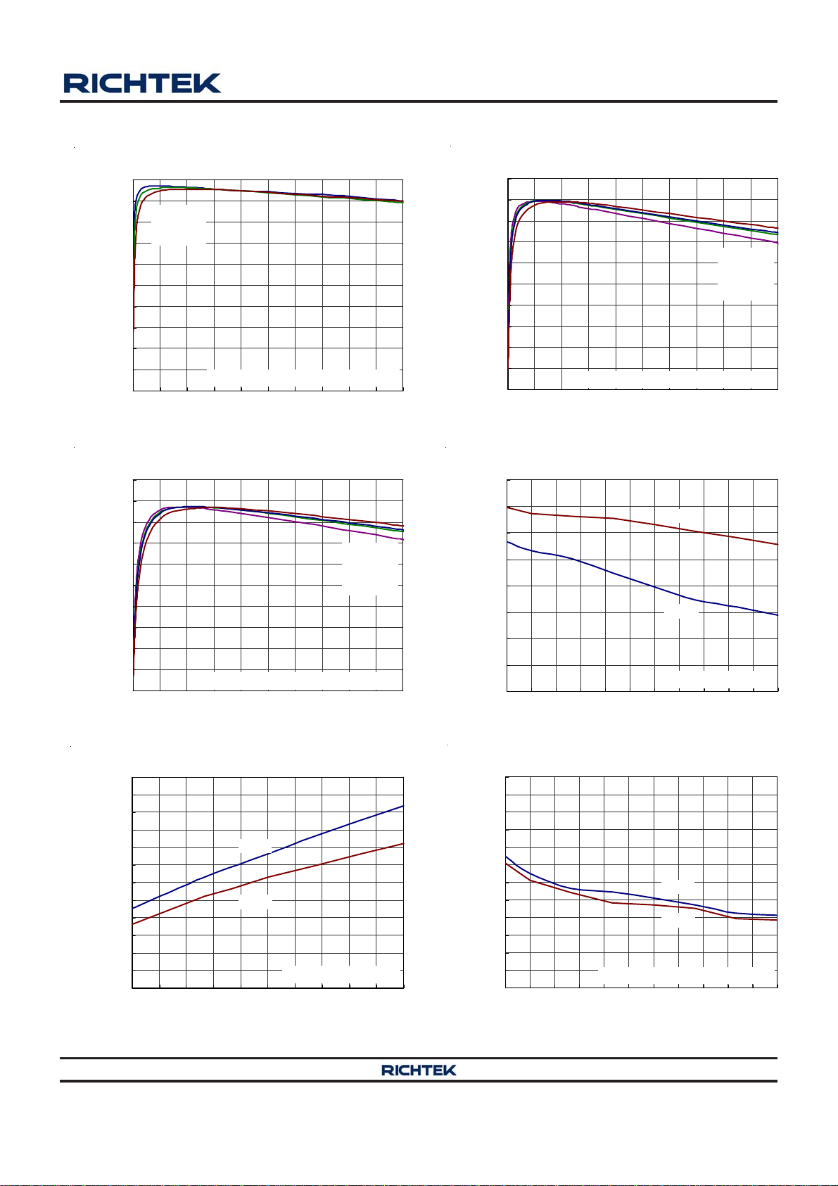
Typical Operating Characteristics
RT8020
Efficiency vs. Output Current
100
90
VIN = 3.6V
VIN = 4.2V
80
VIN = 5.0V
70
60
50
40
Efficiency (%)
30
20
10
0
0 0.1 0.2 0.3 0.4 0.5 0.6 0.7 0.8 0.9 1
V
= 3.3V, L = 4.7μH, C
OUT
Output Current (A)
Efficiency vs. Output Current
100
90
80
70
60
50
40
Efficiency (%)
30
20
10
0
0 0.1 0.2 0.3 0.4 0.5 0.6 0.7 0.8 0.9 1
V
= 1.2V, L = 2.2μH, C
OUT
Output Current (A)
= 4.7μF
OUT
VIN = 5.0V
VIN = 3.6V
VIN = 3.3V
VIN = 2.5V
= 10μF
OUT
Efficiency vs. Output Current
100
90
80
70
60
50
40
Efficiency (%)
30
20
10
0
0 0.1 0.2 0.3 0.4 0.5 0.6 0.7 0.8 0.9 1
V
= 1.2V, L = 4.7μH, C
OUT
Output Current (A)
UVLO Threshold vs. Temperature
2.00
1.90
1.80
1.70
1.60
1.50
1.40
UVLO Threshold (V)
1.30
1.20
-40 -25 -10 5 20 35 50 65 80 95 110 125
Temperature
Rising
Falling
V
OUT
(°C)
= 1.2V, I
VIN = 5.0V
VIN = 3.6V
VIN = 3.3V
VIN = 2.5V
= 4.7μF
OUT
= 0A
OUT
EN Pin Threshold vs. Input Voltage
EN Pin Threshold vs. Input Voltage
1.20
1.15
1.10
1.05
1.00
0.95
0.90
0.85
0.80
0.75
EN Pin Threshold (V)
0.70
0.65
0.60
2.5 2.8 3.1 3.4 3.7 4 4.3 4.6 4.9 5.2 5.5
Rising
Falling
V
OUT
= 1.2V, I
OUT
= 0A
Input Voltage (V)
Copyright 2012 Richtek Technology Corporation. All rights reserved. is a registered trademark of Richtek Technology Corporation.
©
1.6
1.5
1.4
1.3
1.2
1.1
1.0
0.9
0.8
0.7
EN Pin Threshold (V)
0.6
0.5
0.4
EN Pin Threshold vs. Temperature
Rising
Falling
VIN = 3.6V, V
-40 -25 -10 5 20 35 50 65 80 95 110 125
Temperature
OUT
(°C)
= 1.2V, I
OUT
= 0A
DS8020-06 March 2012 www.richtek.com
7
RT8020
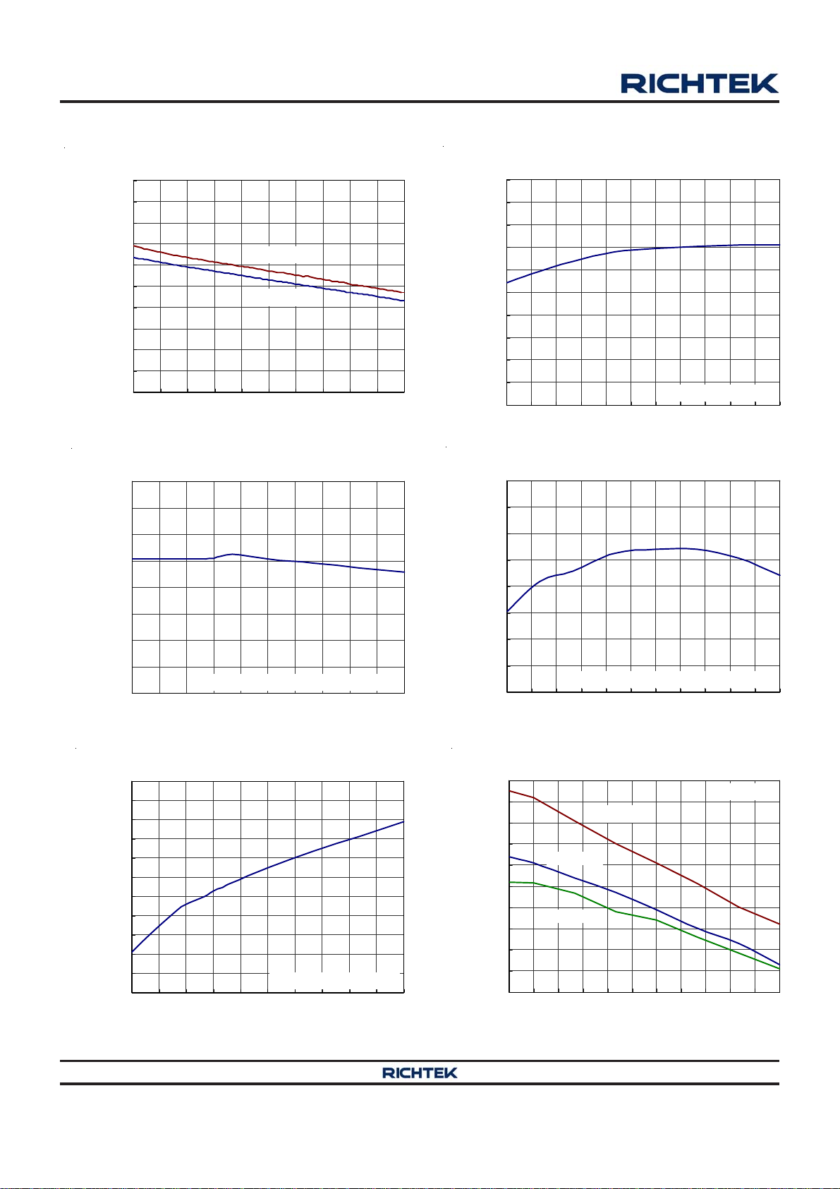
Output Voltage (V)
Output Voltage vs. Loading Current
1.230
1.225
1.220
1.215
1.210
1.205
1.200
1.195
1.190
1.185
1.180
0 0.1 0.2 0.3 0.4 0.5 0.6 0.7 0.8 0.9 1
VIN = 5.0V
VIN = 3.6V
Loading Current (A)
Switching Frequency vs . Input Voltage
1.60
1.55
1.50
1.45
Output Voltage vs. Temperature
1.25
1.24
1.23
1.22
1.21
1.20
1.19
1.18
Output Voltage (V)
1.17
1.16
1.15
-40 -25 -10 5 20 35 50 65 80 95 110 125
Temperature
VIN = 3.6V, I
(°C)
Switching Frequency vs. Temperature
1.6
1.55
1.5
1.45
OUT
= 0A
1.40
1.35
Frequency(kHz)
1.30
1.25
1.20
VIN = 3.6V, V
2.5 2.8 3.1 3.4 3.7 4 4.3 4.6 4.9 5.2 5.5
OUT
= 1.2V, I
OUT
Input Voltage (V)
Output Current Limit vs. Input Voltage
2.4
2.3
2.2
2.1
2.0
1.9
1.8
1.7
1.6
1.5
Output Current Limit (A)
1.4
1.3
2.5 2.8 3.1 3.4 3.7 4 4.3 4.6 4.9 5.2 5.5
Input Voltage (V)
V
OUT
= 1.2V @ T
= 300mA
= 25°C
A
1.4
1.35
Frequency(kHz)
1.3
1.25
1.2
-40 -25 -10 5 20 35 50 65 80 95 110 125
VIN = 3.6V, V
Temperature
OUT
(°C)
= 1.2V, I
OUT
Output Current Limit vs. Tempe rature
2.4
2.3
2.2
2.1
2.0
1.9
1.8
1.7
1.6
Output Current Limit (A)
1.5
1.4
-40 -25 -10 5 20 35 50 65 80 95 110 125
VIN = 5.0V
VIN = 3.6V
VIN = 3.3V
Temperature
(°C)
V
= 300mA
= 1.2V
OUT
Copyright 2012 Richtek Technology Corporation. All rights reserved. is a registered trademark of Richtek Technology Corporation.
©
DS8020-06 March 2012www.richtek.com
8

RT8020
V
EN
(2V/Div)
V
OUT
(1V/Div)
I
IN
(500mA/Div)
V
IN
(2V/Div)
VIN = 3.6V, V
VIN = 3.6V, V
Power On from EN
= 1.2V, I
OUT
Time (100μs/Div)
OUT
= 10mA
Power On from V
= 1.2V, I
OUT
OUT
= 10mA
Power On from EN
VIN = 3.6V, V
V
EN
(2V/Div)
V
OUT
(1V/Div)
I
IN
(500mA/Div)
IN
VIN = 3.6V, V
V
EN
(2V/Div)
= 1.2V, I
OUT
OUT
= 1A
Time (100μs/Div)
Power Off from EN
= 1.2V, I
OUT
OUT
= 10mA
V
OUT
(1V/Div)
I
LX
(1A/Div)
V
OUT
(50mV/Div)
I
OUT
(500mA/Div)
Time (250μs/Div)
Load Transient Response
VIN = 3.6V, V
= 1.2V, I
OUT
OUT
= 50mA to 1A
V
OUT
(1V/Div)
I
LX
(1A/Div)
V
OUT
(50mV/Div)
I
OUT
(500mA/Div)
Time (100μs/Div)
Load Transient Response
VIN = 3.6V, V
OUT
= 1.2V, I
OUT
= 50mA to 0.5A
Time (50μs/Div)
Copyright 2012 Richtek Technology Corporation. All rights reserved. is a registered trademark of Richtek Technology Corporation.
©
Time (50μs/Div)
DS8020-06 March 2012 www.richtek.com
9

RT8020
V
OUT
(50mV/Div)
I
OUT
(500mA/Div)
V
OUT
(10mV/Div)
Load Transient Response
VIN = 5.0V, V
= 1.2V, I
OUT
OUT
Time (50μs/Div)
Ripple
VIN = 3.6V, V
= 1.2V, I
OUT
OUT
= 50mA to 1A
= 1A
V
OUT
(50mV/Div)
I
OUT
(500mA/Div)
V
OUT
(10mV/Div)
Load Transient Response
VIN = 5.0V, V
= 1.2V, I
OUT
Time (50μs/Div)
OUT
Ripple
VIN = 5.0V, V
= 1.2V, I
OUT
OUT
= 50mA to 0.5A
= 1A
V
LX
(2V/Div)
Time (500ns/Div)
V
LX
(2V/Div)
Time (500ns/Div)
Copyright 2012 Richtek Technology Corporation. All rights reserved. is a registered trademark of Richtek Technology Corporation.
©
DS8020-06 March 2012www.richtek.com
10
Applications Information
RT8020
The basic RT8020 application circuit is shown in Typical
Application Circuit. External component selection is
determined by the maximum load current and begins with
the selection of the inductor value and operating frequency
followed by CIN and C
OUT
.
Inductor Selection
For a given input and output voltage, the inductor value
and operating frequency determine the ripple current. The
ripple current ΔI
increases with higher VIN and decreases
L
with higher inductance.
ΔI
V
⎡
=
L
⎢
⎣
⎤
⎥
Lf
×
⎦
V
⎡
1
−×
⎢
⎣
⎤
OUTOUT
⎥
V
IN
⎦
Having a lower ripple current reduces the ESR losses in
the output capacitors and the output voltage ripple. Highest
efficiency operation is achieved at low frequency with small
ripple current. This, however, requires a large inductor.
A reasonable starting point for selecting the ripple current
is ΔIL = 0.4(I
). The largest ripple current occurs at the
MAX
highest VIN. To guarantee that the ripple current stays
below a specified maximum, the inductor value should be
chosen according to the following equation :
⎡
L(MAX)
⎤
⎥
⎦
V
1
−×
⎢
V
IN(MAX)
⎣
⎡
V
L
=
OUT
⎢
If
Δ×
⎣
OUT
⎤
⎥
⎦
Inductor Core Selection
Once the value for L is known, the type of inductor must
be selected. High efficiency converters generally cannot
afford the core loss found in low cost powdered iron cores,
forcing the use of more expensive ferrite or permalloy
cores. Actual core loss is independent of core size for a
fixed inductor value but it is very dependent on the
inductance selected. As the inductance increases, core
losses decrease. However, increased inductance requires
more turns of wire and therefore copper losses will
increase.
Ferrite designs have very low core losses and are preferred
at high switching frequencies, so design goals can
concentrate on copper loss and preventing saturation.
Ferrite core material saturates “hard”, which means that
inductance collapses abruptly when the peak design
current is exceeded.
This results in an abrupt increase in inductor ripple current
and consequent output voltage ripple.
Do not allow the core to saturate!
Different core materials and shapes will change the size/
current and price/current relationship of an inductor. Toroid
or shielded pot cores in ferrite or permalloy materials are
small and don't radiate energy but generally cost more
than powdered iron core inductors with similar
characteristics. The choice of which style inductor to use
mainly depend on the price vs. size requirements and
any radiated field/EMI requirements.
CIN and C
Selection
OUT
The input capacitance, CIN, is needed to filter the
trapezoidal current at the source of the top MOSFET. To
prevent large ripple voltage, a low ESR input capacitor
sized for the maximum RMS current should be used. RMS
current is given by :
V
II
OUT(MAX)RMS
OUT
V
This formula has a maximum at VIN = 2V
I
RMS
= I
/2. This simple worst-case condition is
OUT
V
IN
1
−=
V
OUT
IN
, where
OUT
commonly used for design because even significant
deviations do not offer much relief. Note that ripple current
ratings from capacitor manufacturers are often based on
only 2000 hours of life which makes it advisable to further
de-rate the capacitor, or choose a capacitor rated at a
higher temperature than required. Several capacitors may
also be paralleled to meet size or height requirements in
the design.
The selection of C
is determined by the effective series
OUT
resistance (ESR) that is required to minimize voltage ripple
and load step transients, as well as the amount of bulk
capacitance that is necessary to ensure that the control
loop is stable. Loop stability can be checked by viewing
the load transient response as described in a later section.
The output ripple, ΔV
⎡
ESR ΔIΔV
LOUT
⎢
⎣
, is determined by :
OUT
⎤
1
+≤
8fC
OUT
⎥
⎦
Copyright 2012 Richtek Technology Corporation. All rights reserved. is a registered trademark of Richtek Technology Corporation.
DS8020-06 March 2012 www.richtek.com
©
11

RT8020
The output ripple is highest at maximum input voltage
since ΔIL increases with input voltage. Multiple capacitors
placed in parallel may be needed to meet the ESR and
RMS current handling requirements. Dry tantalum, special
polymer, aluminum electrolytic and ceramic capacitors are
all available in surface mount packages. Special polymer
capacitors offer very low ESR but have lower capacitance
density than other types. Tantalum capacitors have the
highest capacitance density but it is important to only
use types that have been surge tested for use in switching
power supplies. Aluminum electrolytic capacitors have
significantly higher ESR but can be used in cost-sensitive
applications provided that consideration is given to ripple
current ratings and long-term reliability. Ceramic capacitors
have excellent low ESR characteristics but can have a
high voltage coefficient and audible piezoelectric effects.
The high Q of ceramic capacitors with trace inductance
can also lead to significant ringing.
Using Ceramic In put and Output Capacitors
Higher values, lower cost ceramic capacitors are now
becoming available in smaller case sizes. Their high ripple
current, high voltage rating and low ESR make them ideal
for switching regulator applications. However, care must
be taken when these capacitors are used at the input and
output. When a ceramic capacitor is used at the input
and the power is supplied by a wall adapter through long
wires, a load step at the output can induce ringing at the
input, VIN. At best, this ringing can couple to the output
and be mistaken as loop instability. At worst, a sudden
inrush of current through the long wires can potentially
cause a voltage spike at VIN large enough to damage the
part.
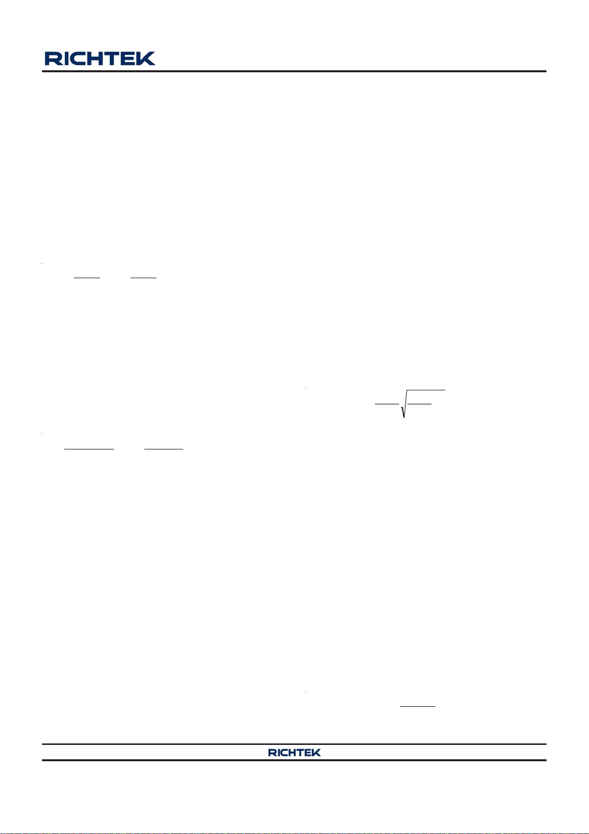
Output Voltage Programming
The resistive divider allows the FB pin to sense a fraction
of the output voltage as shown in Figure 3.
V
OUT
R1
FB
RT8020
GND
R2
Figure 3. Setting the Output Voltage
For adjustable voltage mode, the output voltage is set by
an external resistive divider according to the following
equation :
V
= V
OUT
Where V
x (1+ R1/R2)
REF
is the internal reference voltage (0.6V typical)
REF
Efficiency Considerations
The efficiency of a switching regulator is equal to the output
power divided by the input power times 100%. It is often
useful to analyze individual losses to determine what is
limiting the efficiency and which change would produce
the most improvement. Efficiency can be expressed as :
Efficiency = 100% − (L1+ L2+ L3+...)
where L1, L2, etc. are the individual losses as a percentage
of input power. Although all dissipative elements in the
circuit produce losses, two main sources usually account
for most of the losses: VIN quiescent current and I2R
losses.
The VIN quiescent current loss dominates the efficiency
loss at very low load currents whereas the I2R loss
dominates the efficiency loss at medium to high load
currents. In a typical efficiency plot, the efficiency curve
at very low load currents can be misleading since the
actual power lost is of no consequence.
1.The VIN quiescent current oppears due to two
components : the DC bias current and the gate charge
currents. The gate charge current results from switching
the gate capacitance of the internal power MOSFET
switches. Each time the gate is switched from high to
low to high again, a packet of charge ΔQ moves from V
to ground.
The resulting ΔQ/Δt is the current out of VIN that is typically
larger than the DC bias current. In continuous mode,
I
GATECHG
= f(QT + QB)
where QT and QB are the gate charges of the internal top
and bottom switches. Both the DC bias and gate charge
losses are proportional to VIN and thus their effects will
be more pronounced at higher supply voltages.
2. I2R losses are calculated from the resistances of the
internal switches, RSW and external inductor RL. In
continuous mode the average output current flowing
IN
Copyright 2012 Richtek Technology Corporation. All rights reserved. is a registered trademark of Richtek Technology Corporation.
12
©
DS8020-06 March 2012www.richtek.com

RT8020
through inductor L is “chopped” between the main switch
and the synchronous switch. Thus, the series resistance
looking into the LX pin is a function of both top and bottom
MOSFET R
and the duty cycle (DC) is shown as
DS(ON)
follows :
RSW = R
The R
DS(ON)
DS(ON)TOP
x DC + R
DS(ON)BOT
x (1 − DC)
for both the top and bottom MOSFETs can be
obtained from the Typical Performance Characteristics
curves. Thus, to obtain I2R losses, simply add RSW to R
and multiply the result by the square of the average output
current. Other losses including CIN and C
OUT
ESR
dissipative losses and inductor core losses generally
account for less than 2% of the total loss.
Thermal Considerations
The maximum power dissipation depends on the thermal
resistance of IC package, PCB layout, the rate of
surroundings airflow and temperature difference between
junction to ambient. The maximum power dissipation can
be calculated by following formula :
P
Where T
D(MAX)
= ( T
J(MAX)
− TA ) / θ
J(MAX)
JA
is the maximum junction temperature, TA is
the ambient temperature and the θJA is the junction to
ambient thermal resistance. For recommended operating
conditions specification of RT8020 DC/DC converter,
where T
is the maximum junction temperature of
J(MAX)
the die and TA is the ambient temperature. The junction
to ambient thermal resistance θJA is layout dependent.
For WDFN-12L 3x3 packages, the thermal resistance
θ
is 60°C/W on the standard JEDEC 51-7 four-layers
JA
thermal test board. The maximum power dissipation at
TA = 25°C can be calculated by following formula :
P
= (125°C − 25°C) / (60°C/W) = 1.667W for
D(MAX)
WDFN-12L 3x3 packages
The maximum power dissipation depends on operating
ambient temperature for fixed T
and thermal
J(MAX)
resistance θJA. For RT8020 packages, the Figure 4 of de-
rating curves allows the designer to see the effect of rising
ambient temperature on the maximum power allowed.
1.8
1.6
1.4
1.2
1.0
0.8
0.6
0.4
L
0.2
Maximum Power Dissipation (W)
0.0
0 25 50 75 100 125
Four-Layer PCB
Ambient Temperature (°C)
Figure 4. De-rating Curves for RT8020 Package
Checking Tra n sient Re spon se
The regulator loop response can be checked by looking
at the load transient response. Switching regulators take
several cycles to respond to a step in load current. When
a load step occurs, V
equal to ΔI
resistance of C
discharge C
(ESR), where ESR is the effective series
LOAD
OUT
generating a feedback error signal used
OUT
by the regulator to return V
During this recovery time, V
immediately shifts by an amount
OUT
. ΔI
also begins to charge or
LOAD
to its steady-state value.
OUT
can be monitored for
OUT
overshoot or ringing that would indicate a stability problem.
Layout Considerations
Follow the PCB layout guidelines for optimal performance
of RT8020.
` For the main current paths, keep their traces short and
wide.
` Put the input capacitor as close as possible to the device
pins (VIN and GND).
` LX node is with high frequency voltage swing and should
be kept small area. Keep analog components away from
LX node to prevent stray capacitive noise pick-up.
` Connect feedback network behind the output capacitors.
Keep the loop area small. Place the feedback
components near the RT8020.
` Connect all analog grounds to a command node and
then connect the command node to the power ground
behind the output capacitors.
Copyright 2012 Richtek Technology Corporation. All rights reserved. is a registered trademark of Richtek Technology Corporation.
DS8020-06 March 2012 www.richtek.com
©
13

RT8020
Table 1. Recommended Inductors
Component
Supplier
T AIYO YUDEN NR 3015 2.2 60 1480 3 x 3 x 1.5
T AIYO YUDEN NR 3015 4.7 120 1020 3 x 3 x 1.5
Sumida CDRH2D14 2.2 75 1500 4.5 x 3.2 x 1.55
Sumida CDRH2D14 4.7 135 1000 4.5 x 3.2 x 1.55
GOTREND GTSD32 2.2 58 1500 3.85 x 3.85 x 1.8
GOTREND GTSD32 4.7 146 1 100 3.85 x 3.85 x 1. 8
Series
Inductance
(μH)
DCR
(mΩ)
Current Rati ng
(mA)
Dimensions
(mm)
Table 2. Recomm ended Capacitors for CIN and C
Compon ent Sup pl ie r Part No. Capacit ance (μF) Case Size
TDK C1608JB0J475M 4.7 0603
TDK C2012JB0J106M 10 0805
MURAT A GRM188R60J475KE19 4.7 0603
MURAT A GRM219R60J106ME19 10 0805
TAIYO YUDEN JMK107BJ475RA 4.7 0603
TAIYO YUDEN JMK107BJ106MA 10 0603
TAIYO YUDEN JMK212BJ106RD 10 0805
OUT
Copyright 2012 Richtek Technology Corporation. All rights reserved. is a registered trademark of Richtek Technology Corporation.
14
©
DS8020-06 March 2012www.richtek.com
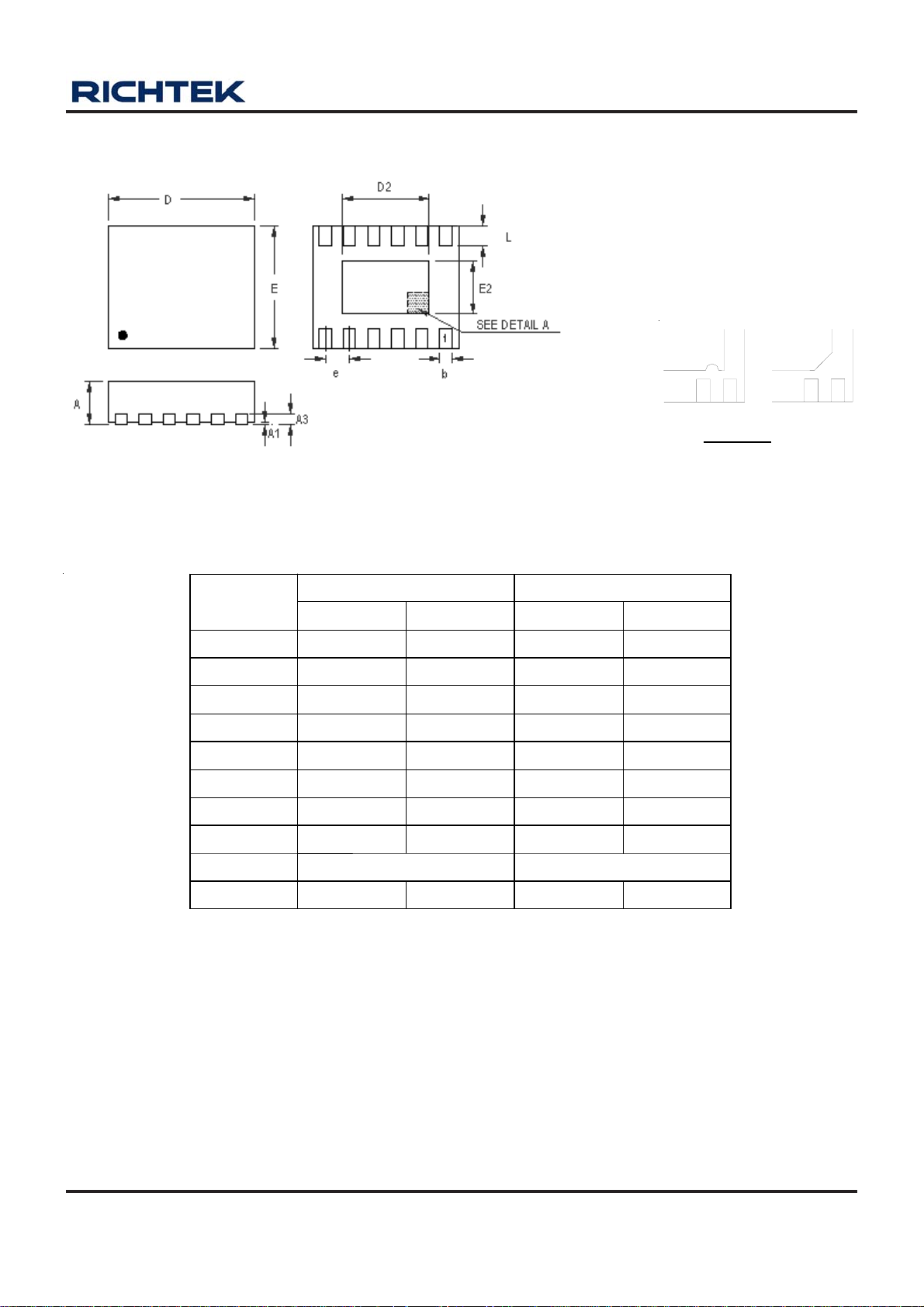
Outline Dimension
RT8020
2
DETAIL A
Pin #1 ID a nd T ie Bar Mark Option s
Note : The configuration of the Pin #1 identifier is optional,
but must be located within the zone indicated.
Dimensions In Millimeters Dimension s In Inches
Symbol
Min Max Min Max
A 0.700 0.800 0.028 0.031
A1 0.000 0.050 0.000 0.002
A3 0.175 0.250 0.007 0.010
b 0.150 0.250 0.006 0.010
D 2.950 3.050 0.116 0.120
D2 2.300 2.650 0.091 0.104
E 2.950 3.050 0.116 0.120
1
1
2
E2 1.400 1.750 0.055 0.069
e 0.450 0.018
L 0.350 0.450
W-Type 12L DFN 3x3 Package
0.014 0.018
Richtek Technology Corporation
5F, No. 20, Taiyuen Street, Chupei City
Hsinchu, Taiwan, R.O.C.
Tel: (8863)5526789
Richtek products are sold by description only. Richtek reserves the right to change the circuitry and/or specifications without notice at any time. Customers should
obtain the latest relevant information and data sheets before placing orders and should verify that such information is current and complete. Richtek cannot
assume responsibility for use of any circuitry other than circuitry entirely embodied in a Richtek product. Information furnished by Richtek is believed to be
accurate and reliable. However, no responsibility is assumed by Richtek or its subsidiaries for its use; nor for any infringements of patents or other rights of third
parties which may result from its use. No license is granted by implication or otherwise under any patent or patent rights of Richtek or its subsidiaries.
DS8020-06 March 2012 www.richtek.com
15

 Loading...