Page 1

Short-Form Datasheet
GX32424
4 x 32Gbps Linear TIA
X0106030 Rev.1.0
Nov.18.20
Page 1
SPI Control
ADC DAC
PD bi as
Filter
MGC/AGC
Gain Monitor
Input Monitor /LOS
OA-Output
Voltag e Contr ol
GC-Gain
Cont rol
Peak
Cont rol
Output Monit or
Cor e
TIA
VGA1
Output
Stage
VGA2
CM Loop
1
DC Offse t
Loop2
DC Offse t
Loop3
Rectif ier
AGC
RSSI
SW
PKD_GC1 SWPKD_GC
2
PKD_GC3
PKD_GC
4
GC_OA1GC_OA2
GC_OA3
GC_OA4
SW
SW
SW
Peaking
MC
SHD
CONFI G
PDS1
PDS2
PDS3
PDS4
PD2
PD3
PD4
PD1
NoCon
PKD_SUM
GC_SUM
LOS
SW
Scale r
SUM
SUM
CH2,3,4
CH2,3,4
CH2 CH3 CH4 CH4CH3CH2
CH2,3,4
In1p
In1n
Out1p
Out1n
SW SW
SHD
CH2,3,4 CH2,3,4
CH1,2,3,4
SUM
CH2,3,4
CH1,2,3,4
CH1,2,3,4
CH1,2,3,4
CS
SCK
MOSI
MISO
RST
CH1,2,3,4
CH1,2,3,4
CH1,2,3,4
VCCi n1
VCCi n2VCCi n3
VCCi n4
VCCo ut1
VCCo ut2
VCCo ut3
VCCo ut4
In2
p
In2n
In3p
In3n
In4p
In4n
Out2p
Out2n
Out4p
Out4n
Out3p
Out3n
The GX32424 is a 32Gbps linear quad TIA chip that
integrates four lanes of TIAs for XI, XQ, YI, and YQ
channels, as well as digital interface circuitry for DC
controls on a single die for 100G/200G coherent
applications. The TIA electrical characteristics,
functions, and physical dimensions are designed for
small-form factor integrated optical modules such as
CFP2 and CFP4.
Applications
• 100G/200G coherent systems with 32Gbps
QPSK/16QAM modulation format
• Integrated optical modules for CFP/CFP2/CFP4
form factors
Features
• Quad 32Gbps linear TIA Integrated SPI and
analog interface
• Differential linear gain: 150–5,000Ω, and > 30dB
dynamic range
• 25+GHz adjustable 3dB bandwidth
• Automatic and manual gain control, output
voltage control, peak detection, RSSI and input
current monitor, and shutdown functionalities
• Low THD, low crosstalk, and low power for
covering 16QAM applications
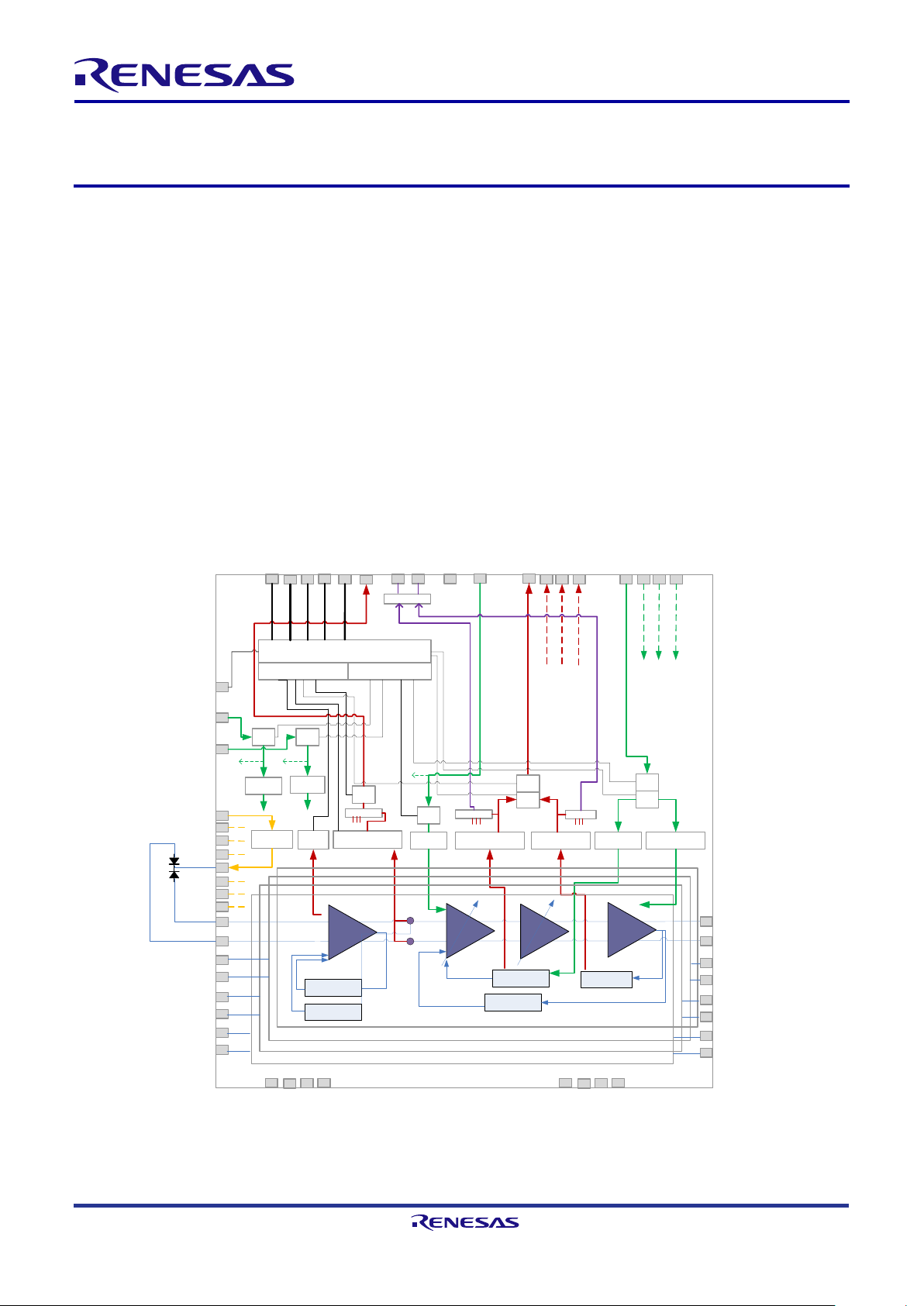
Figure 1. Block Diagram
Page 2

IMPORTANT NOTICE AND DISCLAIMER
RENESAS ELECTRONICS CORPORATION AND ITS SUBSIDIARIES (“RENESAS”) PROVIDES TECHNICAL
SPECIFICATIONS AND RELIABILITY DATA (INCLUDING DATASHEETS), DESIGN RESOURCES (INCLUDING
REFERENCE DESIGNS), APPLICATION OR OTHER DESIGN ADVICE, WEB TOOL S, SAFETY INFORMATION, AND
OTHER RESOURCES “AS IS” AND WITH ALL FAULTS, AND DISCLAIMS ALL WARRANTIES, EXPRESS OR IMPLIED,
INCLUDING, WITHOUT LIMITATION, ANY IMPLIED WARRANTIES OF MERCHANTABILITY, FITNESS FOR A
PARTICULAR PURPOSE, OR NON-INFRINGEMENT OF THIRD PARTY INTELLECTUAL PROPERTY RIGHTS.
These resources are intended for developers skilled in the art designing with Renesas products. You are solely responsible
for (1) selecting the appropriate products for your application, (2) designing, validating, and testing your application, and (3)
ensuring your application meets applicable standards, and any other safety, security, or other requirements. These
resources are subject to change without notice. Renesas grants you permission to use these resources only for
development of an application that uses Renesas products. Other reproduction or use of these resources is strictly
prohibited. No license is granted to any other Renesas intellectual property or to any third party intellectual property.
Renesas disclaims responsibility for, and you will fully indemnify Renesas and its representatives against, any claims,
damages, costs, losses, or liabilities arising out of your use of these resources. Renesas' products are provided only subject
to Renesas' Terms and Conditions of Sale or other applicable terms agreed to in writing. No use of any Renesas resources
expands or otherwise alters any applicable warranties or warranty disclaimers for these products.
Corporate Headquarters
TOYOSU FORESIA, 3-2-24 Toyosu,
Koto-ku, Tokyo 135-0061, Japan
www.renesas .com
Trademarks
Renesas and the Renesas logo are trademarks of Renesas
Electronics Corporation. All trademarks and registered
trademarks are the property of their respective owners.
(Rev.1.0 Mar 2020)
Contact Information
For further information on a product, technology, the most
up-to-date version of a document, or your nearest sales
office, please visit:
www.renesas .com/contact/
© 2020 Renesas Electronics Corporation. All rights reserved.
 Loading...