

Page 1

User’s Manual
A
RL78/G1
16
User’s Manual: Hardware
16-Bit Single-Chip Microcontrollers
All information contained in these materials, including products and product specifications,
represents information on the product at the time of publication and is subject to change by
Renesas Electronics Corp. without notice. Please review the latest information published by
Renesas Electronics Corp. through various means, including the Renesas Electronics Corp.
website (http://www.renesas.com).
www.renesas.com
Rev.2.00 Jul 2013
Page 2

Notice
1. Descriptions of circuits, software and other related information in this document are provided only to illustrate the operation of
semiconductor products and application examples. You are fully responsible for the incorporation of these circuits, software,
and information in the design of your equipment. Renesas Electronics assumes no responsibility for any losses incurred by you
or third parties arising from the use of these circuits, software, or information.
2. Renesas Electronics has used reasonable care in preparing the information included in this document, but Renesas Electronics
does not warrant that such information is error free. Renesas Electronics assumes no liability whatsoever for any damages
incurred by you resulting from errors in or omissions from the information included herein.
3. Renesas Electronics does not assume any liability for infringement of patents, copyrights, or other intellectual property rights of
third parties by or arising from the use of Renesas Electronics products or technical information described in this document. No
license, express, implied or otherwise, is granted hereby under any patents, copyrights or other intellectual property rights of
Renesas Electronics or others.
4. You should not alter, modify, copy, or otherwise misappropriate any Renesas Electronics product, whether in whole or in part.
Renesas Electronics assumes no responsibility for any losses incurred by you or third parties arising from such alteration,
modification, copy or otherwise misappropriation of Renesas Electronics product.
5. Renesas Electronics products are classified according to the following two quality grades: “Standard” and “High Quality”. The
recommended applications for each Renesas Electronics product depends on the product’s quality grade, as indicated below.
“Standard”: Computers; office equipment; communications equipment; test and measurement equipment; audio and visual
equipment; home electronic appliances; machine tools; personal electronic equipment; and industrial robots etc.
“High Quality”: Transportation equipment (automobiles, trains, ships, etc.); traffic control syst ems; anti-disaster systems; anti-
crime systems; and safety equipment etc.
Renesas Electronics products are neither intended nor authorized for use in products or systems that may pose a direct threat to
human life or bodily injury (artificial life support devices or systems, surgical implantations etc.), or may cause serious property
damages (nuclear reactor control systems, military equipment etc.). You must check the quality grade of each Renesas
Electronics product before using it in a particular application. You may not use any Renesas Electronics product for any
application for which it is not intended. Renesas Electronics shall not be in any way liable for any damages or losses incurred
by you or third parties arising from the use of any Renesas Electronics product for which the product is not intended by Renesas
Electronics.
6. You should use the Renesas Electronics products described in this document within the range specified by Renesas Electronics,
especially with respect to the maximum rating, operating supply voltage range, movement power voltage range, heat radiation
characteristics, installation and other product characteristics. Renesas Electronics shall have no liability for malfunctions or
damages arising out of the use of Renesas Electronics products beyond such specified ranges.
7. Although Renesas Electronics endeavors to improve the quality and reliability of its products, semiconductor products have
specific characteristics such as the occurrence of failure at a certain rate and malfunctions under certain use conditions. Further,
Renesas Electronics products are not subject to radiation resistance design. Please be sure to implement safety measures to
guard them against the possibility of physical injury, and injury or damage caused by fire in the event of the failure of a Renesas
Electronics product, such as safety design for hardware and software including but not limited to redundancy, fire control and
malfunction prevention, appropriate treatment for aging degradation or any other appropriate measures. Because the evaluation
of microcomputer software alone is very difficult, please evaluate the safety of the final products or systems manufactured by
you.
8. Please contact a Renesas Electronics sales office for details as to environmental matters such as the environmental compatibility
of each Renesas Electronics product. Please use Renesas Electronics products in compliance with all applicable laws and
regulations that regulate the inclusion or use of controlled substances, including without limitation, the EU RoHS Directive.
Renesas Electronics assumes no liability for damages or losses occurring as a result of your noncompliance with applicable laws
and regulations.
9. Renesas Electronics products and technology may not be used for or incorporated into any products or systems whose
manufacture, use, or sale is prohibited under any applicable domestic or foreign laws or regulations. You should not use
Renesas Electronics products or technology described in this document for any purpose relating to military applications or use
by the military, including but not limited to the development of weapons of mass destruction. When exporting the Renesas
Electronics products or technology described in this document, you should comply with the applicable export control laws and
regulations and follow the procedures required by such laws and regulations.
10. It is the responsibility of the buyer or distributor of Renesas Electronics products, who distributes, disposes of, or otherwise
places the product with a third party, to notify such third party in advance of the contents and conditions set forth in this
document, Renesas Electronics assumes no responsibility for any losses incurred by you or third parties as a result of
unauthorized use of Renesas Electronics products.
11. This document may not be reproduced or duplicated in any form, in whole or in part, without prior written consent of Renesas
Electronics.
12. Please contact a Renesas Electronics sales office if you have any questions regarding the information contained in this document
or Renesas Electronics products, or if you have any other inquiries.
(Note 1) “Renesas Electronics” as used in this document means Renesas Electronics Corporation and also includes its majority-
owned subsidiaries.
(Note 2) “Renesas Electronics product(s)” means any product developed or manufactured by or for Renesas Electronics.
(2012.4)
Page 3

NOTES FOR CMOS DEVICES
(1) VOLTAGE APPLICATION WAVEFORM AT INPUT PIN: Waveform distortion due to input noise or a
reflected wave may cause malfunction. If the input of the CMOS device stays in the area between VIL
(MAX) and VIH (MIN) due to noise, etc., the device may malfunction. Take care to prevent chattering noise
from entering the device when the input level is fixed, and also in the transition period when the input level
passes through the area between VIL (MAX) and VIH (MIN).
(2) HANDLING OF UNUSED INPUT PINS: Unconnected CMOS device inputs can be cause of malfunction. If
an input pin is unconnected, it is possible that an internal input level may be generated due to noise, etc.,
causing malfunction. CMOS devices behave differently than Bipolar or NMOS devices. Input levels of
CMOS devices must be fixed high or low by using pull-up or pull-down circuitry. Each unused pin should be
connected to VDD or GND via a resistor if there is a possibility that it will be an output pin. All handling
related to unused pins must be judged separately for each device and according to related specifications
governing the device.
(3) PRECAUTION AGAINST ESD: A strong electric field, when exposed to a MOS device, can cause
destruction of the gate oxide and ultimately degrade the device operation. Steps must be taken to stop
generation of static electricity as much as possible, and quickly dissipate it when it has occurred.
Environmental control must be adequate. When it is dry, a humidifier should be used. It is recommended
to avoid using insulators that easily build up static electricity. Semiconductor devices must be stored and
transported in an anti-static container, static shielding bag or conductive material. All test and measurement
tools including work benches and floors should be grounded. The operator should be grounded using a wrist
strap. Semiconductor devices must not be touched with bare hands. Similar precautions need to be taken
for PW boards with mounted semiconductor devices.
(4) STATUS BEFORE INITIALIZATION: Power-on does not necessarily define the initial status of a MOS
device. Immediately after the power source is turned ON, devices with reset functions have not yet been
initialized. Hence, power-on does not guarantee output pin levels, I/O settings or contents of registers. A
device is not initialized until the reset signal is received. A reset operation must be executed immediately
after power-on for devices with reset functions.
(5) POWER ON/OFF SEQUENCE: In the case of a device that uses different power supplies for the internal
operation and external interface, as a rule, switch on the external power supply after switching on the internal
power supply. When switching the power supply off, as a rule, switch off the external power supply and then
the internal power supply. Use of the reverse power on/off sequences may result in the application of an
overvoltage to the internal elements of the device, causing malfunction and degradation of internal elements
due to the passage of an abnormal current. The correct power on/off sequence must be judged separately
for each device and according to related specifications governing the device.
(6) INPUT OF SIGNAL DURING POWER OFF STATE : Do not input signals or an I/O pull-up power supply
while the device is not powered. The current injection that results from input of such a signal or I/O pull-up
power supply may cause malfunction and the abnormal current that passes in the device at this time may
cause degradation of internal elements. Input of signals during the power off state must be judged
separately for each device and according to related specifications governing the device.
Page 4

How to Use This Manual
Readers This manual is intended for user engineers who wish to understand the functions of the
RL78/G1A and design and develop application systems and programs for these devices.
The target products are as follows.
• 25-pin: R5F10E8x (x = A, C, D, E)
• 32-pin: R5F10EBx (x = A, C, D, E)
• 48-pin: R5F10EGx (x = A, C, D, E)
• 64-pin: R5F10ELx (x = C, D, E)
Purpose This manual is intended to give users an understanding of the functions described in the
Organization below.
Organization The RL78/G1A manual is separated into two parts: this manual and the instructions edition
(common to the RL78 Microcontroller).
RL78/G1A
User’s Manual
(This Manual)
• Pin functions
• Internal block functions
• Interrupts
• Other on-chip peripheral functions
• Electrical specifications
How to Read This Manual It is assumed that the readers of this manual have general knowledge of electrical
engineering, logic circuits, and microcontrollers.
• To gain a general understanding of functions:
→ Read this manual in the order of the CONTENTS. The mark “<R>” shows major
revised points. The revised points can be easily searched by copying an “<R>” in the
PDF file and specifying it in the “Find what:” field.
• How to interpret the register format:
→ For a bit number enclosed in angle brackets, the bit name is defined as a reserved
word in the assembler, and is defined as an sfr variable using the #pragma sfr
directive in the compiler.
• To know details of the RL78G1A Microcontroller instructions:
→ Refer to the separate document RL78 Microcontroller Instructions User’s Manual
(R01US0015E).
• CPU functions
• Instruction set
• Explanation of each instruction
RL78 Microcontroller
User’s Manual
Instructions
Page 5
Conventions Data significance: Higher digits on the left and lower digits on the right
Active low representations: ××× (overscore over pin and signal name)
Note: Footnote for item marked with Note in the text
Caution: Information requiring particular attention
Remark: Supplementary information
Numerical representations: Binary
Decimal
Hexadecimal
...
×××× or ××××B
...
××××
...
××××H
Related Documents The related documents indicated in this publication may include preliminary versions.
However, preliminary versions are not marked as such.
Documents Related to Devices
Document Name Document No.
RL78/G1A User’s Manual Hardware This manual
RL78 family User’s Manual: Software R01US0015E
Documents Related to Flash Memory Programming
Document Name Document No.
PG-FP5 Flash Memory Programmer User’s Manual R20UT0008E
Caution The related documents listed above are subject to change without notice. Be sure to use the latest
version of each document when designing.
Page 6

Other Documents
Document Name Document No.
Renesas MPUs & MCUs RL78 Family R01CP0003E
Semiconductor Package Mount Manual Note
Quality Grades on NEC Semiconductor Devices C11531E
Guide to Prevent Damage for Semiconductor Devices by Electrostatic Discharge (ESD) C11892E
Semiconductor Reliability Handbook R51ZZ0001E
Note See the “Semiconductor Package Mount Manual” website (http://www.renesas.com/products/package/manual/index.jsp).
Caution The related documents listed above are subject to change without notice. Be sure to use the latest
version of each document when designing.
All trademarks and registered trademarks are the property of their respective owners.
EEPROM is a trademark of Renesas Electronics Corporation.
SuperFlash is a registered trademark of Silicon Storage Technology, Inc. in several countries including the United States
and Japan.
®
Caution: This product uses SuperFlash
technology licensed from Silicon Storage Technology, Inc.
Page 7

CONTENTS
CHAPTER 1 OUTLINE............................................................................................................................... 1
1.1 Features ....................................................................................................................................... 1
1.2 List of Part Numbers................................................................................................................... 4
1.3 Pin Configuration (Top View)..................................................................................................... 6
1.3.1 25-pin products ............................................................................................................................... 6
1.3.2 32-pin products ............................................................................................................................... 7
1.3.3 48-pin products ............................................................................................................................... 8
1.3.4 64-pin products ............................................................................................................................. 10
1.4 Pin Identification ....................................................................................................................... 12
1.5 Block Diagram ........................................................................................................................... 13
1.5.1 25-pin products ............................................................................................................................. 13
1.5.2 32-pin products ............................................................................................................................. 14
1.5.3 48-pin products ............................................................................................................................. 15
1.5.4 64-pin products ............................................................................................................................. 16
1.6 Outline of Functions ................................................................................................................. 17
CHAPTER 2 PIN FUNCTIONS ............................................................................................................... 19
2.1 Port Function............................................................................................................................. 19
2.1.1 25-pin products ............................................................................................................................. 20
2.1.2 32-pin products ............................................................................................................................. 22
2.1.3 48-pin products ............................................................................................................................. 24
2.1.4 64-pin products ............................................................................................................................. 26
2.2 Functions Other than Port Pins ............................................................................................... 29
2.2.1 With functions for each product .................................................................................................... 29
2.2.2 Explanation of function.................................................................................................................. 33
2.3 Pin I/O Circuits and Recommended Connection of Unused Pins........................................ 35
2.4 Block Diagrams of Pins ............................................................................................................ 36
CHAPTER 3 CPU ARCHITECTURE ...................................................................................................... 47
3.1 Memory Space........................................................................................................................... 47
3.1.1 Internal program memory space ................................................................................................... 54
3.1.2 Mirror area .................................................................................................................................... 57
3.1.3 Internal data memory space ......................................................................................................... 59
3.1.4 Special function register (SFR) area............................................................................................. 60
3.1.5 Extended special function register (2nd SFR: 2nd Special Function Register) area..................... 60
3.1.6 Data memory addressing.............................................................................................................. 61
3.2 Processor Registers ................................................................................................................. 62
3.2.1 Control registers ........................................................................................................................... 62
3.2.2 General-purpose registers ............................................................................................................ 64
3.2.3 ES and CS registers ..................................................................................................................... 65
3.2.4 Special function registers (SFRs) ................................................................................................. 66
3.2.5 Extended special function registers (2nd SFRs) ........................................................................... 72
Index-1
Page 8

3.3 Instruction Address Addressing ............................................................................................. 79
3.3.1 Relative addressing ...................................................................................................................... 79
3.3.2 Immediate addressing................................................................................................................... 79
3.3.3 Table indirect addressing.............................................................................................................. 80
3.3.4 Register direct addressing ............................................................................................................ 81
3.4 Addressing for Processing Data Addresses.......................................................................... 82
3.4.1 Implied addressing........................................................................................................................ 82
3.4.2 Register addressing...................................................................................................................... 82
3.4.3 Direct addressing.......................................................................................................................... 83
3.4.4 Short direct addressing................................................................................................................. 84
3.4.5 SFR addressing ............................................................................................................................ 85
3.4.6 Register indirect addressing ......................................................................................................... 86
3.4.7 Based addressing ......................................................................................................................... 87
3.4.8 Based indexed addressing............................................................................................................ 91
3.4.9 Stack addressing .......................................................................................................................... 92
CHAPTER 4 PORT FUNCTIONS ........................................................................................................... 96
4.1 Port Functions........................................................................................................................... 96
4.2 Port Configuration..................................................................................................................... 97
4.2.1 Port 0 ............................................................................................................................................ 98
4.2.2 Port 1 ............................................................................................................................................ 98
4.2.3 Port 2 ............................................................................................................................................ 99
4.2.4 Port 3 ............................................................................................................................................ 99
4.2.5 Port 4 .......................................................................................................................................... 100
4.2.6 Port 5 .......................................................................................................................................... 100
4.2.7 Port 6 .......................................................................................................................................... 100
4.2.8 Port 7 .......................................................................................................................................... 101
4.2.9 Port 12 ........................................................................................................................................ 101
4.2.10 Port 13 ........................................................................................................................................ 101
4.2.11 Port 14 ........................................................................................................................................ 102
4.2.12 Port 15 ........................................................................................................................................ 102
4.3 Registers Controlling Port Function ..................................................................................... 103
4.3.1 Port mode registers (PMxx) ........................................................................................................ 105
4.3.2 Port registers (Pxx) ..................................................................................................................... 106
4.3.3 Pull-up resistor option registers (PUxx)....................................................................................... 107
4.3.4 Port input mode registers (PIMxx) .............................................................................................. 108
4.3.5 Port output mode registers (POMxx) .......................................................................................... 109
4.3.6 Port mode control registers (PMCxx).......................................................................................... 110
4.3.7 A/D port configuration register (ADPC)....................................................................................... 111
4.3.8 Peripheral I/O redirection register (PIOR)................................................................................... 112
4.3.9 Global digital input disable register (GDIDIS) ............................................................................. 113
4.3.10 Global analog input disable register (GAIDIS) ............................................................................ 114
4.4 Port Function Operations....................................................................................................... 115
4.4.1 Writing to I/O port........................................................................................................................ 115
4.4.2 Reading from I/O port ................................................................................................................. 115
4.4.3 Operations on I/O port ................................................................................................................ 115
Index-2
Page 9

4.4.4 Handling different potential (1.8 V or 2.5 V) by using EV
4.4.5 Handling different potential (1.8 V or 2.5 V) by using I/O buffers ................................................ 116
DD ≤ VDD............................................... 116
4.5 Register Settings When Using Alternate Function.............................................................. 118
4.5.1 Basic concept when using alternate function .............................................................................. 118
4.5.2 Register settings for alternate function whose output function is not used ................................. 119
4.5.3 Register setting examples for used port and alternate functions ................................................ 120
4.6 Cautions When Using Port Function..................................................................................... 137
4.6.1 Cautions on 1-bit manipulation instruction for port register n (Pn) .............................................. 137
4.6.2 Notes on specifying the pin settings ........................................................................................... 138
CHAPTER 5 CLOCK GENERATOR .................................................................................................... 139
5.1 Functions of Clock Generator................................................................................................ 139
5.2 Configuration of Clock Generator ......................................................................................... 141
5.3 Registers Controlling Clock Generator................................................................................. 143
5.3.1 Clock operation mode control register (CMC)............................................................................. 143
5.3.2 System clock control register (CKC) ........................................................................................... 146
5.3.3 Clock operation status control register (CSC)............................................................................. 147
5.3.4 Oscillation stabilization time counter status register (OSTC) ...................................................... 148
5.3.5 Oscillation stabilization time select register (OSTS) ................................................................... 150
5.3.6 Peripheral enable register 0 (PER0) ........................................................................................... 152
5.3.7 Subsystem clock supply mode control register (OSMC)............................................................. 155
5.3.8 High-speed on-chip oscillator frequency select register (HOCODIV).......................................... 156
5.3.9 High-speed on-chip oscillator trimming register (HIOTRM)......................................................... 157
5.4 System Clock Oscillator ......................................................................................................... 158
5.4.1 X1 oscillator ................................................................................................................................ 158
5.4.2 XT1 oscillator .............................................................................................................................. 158
5.4.3 High-speed on-chip oscillator...................................................................................................... 162
5.4.4 Low-speed on-chip oscillator ...................................................................................................... 162
5.5 Clock Generator Operation .................................................................................................... 163
5.6 Controlling Clock .................................................................................................................... 165
5.6.1 Example of setting high-speed on-chip oscillator........................................................................ 165
5.6.2 Example of setting X1 oscillation clock ....................................................................................... 166
5.6.3 Example of setting XT1 oscillation clock ..................................................................................... 167
5.6.4 CPU clock status transition diagram ........................................................................................... 168
5.6.5 Condition before changing CPU clock and processing after changing CPU clock...................... 174
5.6.6 Time required for switchover of CPU clock and system clock..................................................... 176
5.6.7 Conditions before clock oscillation is stopped............................................................................. 177
5.7 Resonator and Oscillator Constants..................................................................................... 178
CHAPTER 6 TIMER ARRAY UNIT...................................................................................................... 182
6.1 Functions of Timer Array Unit ............................................................................................... 184
6.1.1 Independent channel operation function..................................................................................... 184
6.1.2 Simultaneous channel operation function ................................................................................... 185
6.1.3 8-bit timer operation function (channels 1 and 3 only) ................................................................ 186
6.1.4 LIN-bus supporting function (channel 7 of unit 0 only)................................................................ 187
6.2 Configuration of Timer Array Unit ......................................................................................... 188
Index-3
Page 10

6.2.1 Timer count register mn (TCRmn) .............................................................................................. 193
6.2.2 Timer data register mn (TDRmn)................................................................................................ 195
6.3 Registers Controlling Timer Array Unit ................................................................................ 196
6.3.1 Peripheral enable register 0 (PER0) ........................................................................................... 197
6.3.2 Timer clock select register m (TPSm)......................................................................................... 198
6.3.3 Timer mode register mn (TMRmn).............................................................................................. 201
6.3.4 Timer status register mn (TSRmn).............................................................................................. 206
6.3.5 Timer channel enable status register m (TEm)........................................................................... 207
6.3.6 Timer channel start register m (TSm) ......................................................................................... 208
6.3.7 Timer channel stop register m (TTm).......................................................................................... 209
6.3.8 Timer input select register 0 (TIS0)............................................................................................. 210
6.3.9 Timer output enable register m (TOEm) ..................................................................................... 211
6.3.10 Timer output register m (TOm) ................................................................................................... 212
6.3.11 Timer output level register m (TOLm) ......................................................................................... 213
6.3.12 Timer output mode register m (TOMm)....................................................................................... 214
6.3.13 Input switch control register (ISC)............................................................................................... 215
6.3.14 Noise filter enable register 1 (NFEN1) ........................................................................................ 216
6.3.15 Registers controlling port functions of pins to be used for timer I/O............................................ 218
6.4 Basic Rules of Timer Array Unit ............................................................................................ 219
6.4.1 Basic rules of simultaneous channel operation function ............................................................. 219
6.4.2 Basic rules of 8-bit timer operation function (channels 1 and 3 only).......................................... 221
6.5 Operation of Counter .............................................................................................................. 222
6.5.1 Count clock (fTCLK)....................................................................................................................... 222
6.5.2 Start timing of counter................................................................................................................. 224
6.5.3 Operation of counter ................................................................................................................... 225
6.6 Channel Output (TOmn Pin) Control ..................................................................................... 230
6.6.1 TOmn pin output circuit configuration ......................................................................................... 230
6.6.2 TOmn pin output setting.............................................................................................................. 231
6.6.3 Cautions on channel output operation ........................................................................................ 232
6.6.4 Collective manipulation of TOmn bit ........................................................................................... 237
6.6.5 Timer Interrupt and TOmn pin output at operation start.............................................................. 238
6.7 Timer Input (TImn) Control..................................................................................................... 239
6.7.1 TImn pin input circuit configuration ............................................................................................. 239
6.7.2 Noise filter................................................................................................................................... 239
6.7.3 Cautions on channel input .......................................................................................................... 240
6.8 Independent Channel Operation Function of Timer Array Unit ......................................... 241
6.8.1 Operation as interval timer/square wave output.......................................................................... 241
6.8.2 Operation as external event counter........................................................................................... 247
6.8.3 Operation as frequency divider (channel 0 of unit 0 only)........................................................... 252
6.8.4 Operation as input pulse interval measurement.......................................................................... 256
6.8.5 Operation as input signal high-/low-level width measurement .................................................... 260
6.8.6 Operation as delay counter......................................................................................................... 264
6.9 Simultaneous Channel Operation Function of Timer Array Unit ....................................... 269
6.9.1 Operation as one-shot pulse output function .............................................................................. 269
6.9.2 Operation as PWM function ........................................................................................................ 276
6.9.3 Operation as multiple PWM output function................................................................................ 283
6.10 Cautions When Using Timer Array Unit................................................................................ 291
Index-4
Page 11

6.10.1 Cautions when using timer output............................................................................................... 291
CHAPTER 7 REAL-TIME CLOCK........................................................................................................ 292
7.1 Functions of Real-time Clock................................................................................................. 292
7.2 Configuration of Real-time Clock .......................................................................................... 293
7.3 Registers Controlling Real-time Clock.................................................................................. 295
7.3.1 Peripheral enable register 0 (PER0) ........................................................................................... 296
7.3.2 Subsystem clock supply mode control register (OSMC)............................................................. 297
7.3.3 Real-time clock control register 0 (RTCC0) ................................................................................ 298
7.3.4 Real-time clock control register 1 (RTCC1) ................................................................................ 299
7.3.5 Second count register (SEC) ...................................................................................................... 301
7.3.6 Minute count register (MIN) ........................................................................................................ 301
7.3.7 Hour count register (HOUR) ....................................................................................................... 302
7.3.8 Day count register (DAY)............................................................................................................ 304
7.3.9 Week count register (WEEK) ...................................................................................................... 305
7.3.10 Month count register (MONTH)................................................................................................... 306
7.3.11 Year count register (YEAR) ........................................................................................................ 306
7.3.12 Watch error correction register (SUBCUD) ................................................................................. 307
7.3.13 Alarm minute register (ALARMWM)............................................................................................ 308
7.3.14 Alarm hour register (ALARMWH)................................................................................................ 308
7.3.15 Alarm week register (ALARMWW).............................................................................................. 308
7.3.16 Port mode register 3 (PM3)......................................................................................................... 309
7.3.17 Port register 3 (P3) ..................................................................................................................... 309
7.4 Real-time Clock Operation ..................................................................................................... 310
7.4.1 Starting operation of real-time clock ........................................................................................... 310
7.4.2 Shifting to HALT/STOP mode after starting operation ................................................................ 311
7.4.3 Reading/writing real-time clock ................................................................................................... 312
7.4.4 Setting alarm of real-time clock................................................................................................... 314
7.4.5 1 Hz output of real-time clock ..................................................................................................... 315
7.4.6 Example of watch error correction of real-time clock .................................................................. 316
CHAPTER 8 12-BIT INTERVAL TIMER .............................................................................................. 321
8.1 Functions of 12-bit Interval Timer ......................................................................................... 321
8.2 Configuration of 12-bit Interval Timer ................................................................................... 321
8.3 Registers Controlling 12-bit Interval Timer ..........................................................................322
8.3.1 Peripheral enable register 0 (PER0) ........................................................................................... 322
8.3.2 Subsystem clock supply mode control register (OSMC)............................................................. 323
8.3.3 Interval timer control register (ITMC) .......................................................................................... 324
8.4 12-bit Interval Timer Operation.............................................................................................. 325
8.4.1 12-bit interval timer operation timing........................................................................................... 325
8.4.2 Starting counter operation after returning from HALT or STOP mode and then shifting to
HALT or STOP mode again ........................................................................................................ 326
CHAPTER 9 CLOCK OUTPUT/BUZZER OUTPUT CONTROLLER ................................................. 327
9.1 Functions of Clock Output/Buzzer Output Controller ......................................................... 327
Index-5
Page 12

9.2 Configuration of Clock Output/Buzzer Output Controller................................................... 329
9.3 Registers Controlling Clock Output/Buzzer Output Controller.......................................... 329
9.3.1 Clock output select registers n (CKSn) ....................................................................................... 329
9.3.2 Registers controlling port functions of pins to be used for clock or buzzer output....................... 331
9.4 Operations of Clock Output/Buzzer Output Controller ....................................................... 332
9.4.1 Operation as output pin............................................................................................................... 332
9.5 Cautions of Clock Output/Buzzer Output Controller........................................................... 332
CHAPTER 10 WATCHDOG TIMER ..................................................................................................... 333
10.1 Functions of Watchdog Timer ............................................................................................... 333
10.2 Configuration of Watchdog Timer......................................................................................... 334
10.3 Register Controlling Watchdog Timer .................................................................................. 335
10.3.1 Watchdog timer enable register (WDTE) .................................................................................... 335
10.4 Operation of Watchdog Timer................................................................................................ 336
10.4.1 Controlling operation of watchdog timer...................................................................................... 336
10.4.2 Setting overflow time of watchdog timer ..................................................................................... 337
10.4.3 Setting window open period of watchdog timer........................................................................... 338
10.4.4 Setting watchdog timer interval interrupt..................................................................................... 339
CHAPTER 11 A/D CONVERTER ......................................................................................................... 340
11.1 Function of A/D Converter ..................................................................................................... 340
11.2 Configuration of A/D Converter............................................................................................. 343
11.3 Registers Used in A/D Converter........................................................................................... 345
11.3.1 Peripheral enable register 0 (PER0) ........................................................................................... 346
11.3.2 A/D converter mode register 0 (ADM0)....................................................................................... 347
11.3.3 A/D converter mode register 1 (ADM1)....................................................................................... 359
11.3.4 A/D converter mode register 2 (ADM2)....................................................................................... 360
11.3.5 12-bit A/D conversion result register (ADCR) ............................................................................. 362
11.3.6 8-bit A/D conversion result register (ADCRH)............................................................................. 363
11.3.7 Analog input channel specification register (ADS) ...................................................................... 364
11.3.8 Conversion result comparison upper limit setting register (ADUL).............................................. 366
11.3.9 Conversion result comparison lower limit setting register (ADLL)............................................... 366
11.3.10 A/D test register (ADTES)........................................................................................................... 367
11.3.11 Registers controlling port function of analog input pins............................................................... 368
11.4 A/D Converter Conversion Operations ................................................................................. 369
11.5 Input Voltage and Conversion Results ................................................................................. 371
11.6 A/D Converter Operation Modes............................................................................................ 372
11.6.1 Software trigger mode (select mode, sequential conversion mode) ........................................... 372
11.6.2 Software trigger mode (select mode, one-shot conversion mode).............................................. 373
11.6.3 Software trigger mode (scan mode, sequential conversion mode) ............................................. 374
11.6.4 Software trigger mode (scan mode, one-shot conversion mode)................................................ 375
11.6.5 Hardware trigger no-wait mode (select mode, sequential conversion mode).............................. 376
11.6.6 Hardware trigger no-wait mode (select mode, one-shot conversion mode)................................ 377
11.6.7 Hardware trigger no-wait mode (scan mode, sequential conversion mode) ............................... 378
11.6.8 Hardware trigger no-wait mode (scan mode, one-shot conversion mode).................................. 379
11.6.9 Hardware trigger wait mode (select mode, sequential conversion mode)................................... 380
Index-6
Page 13

11.6.10 Hardware trigger wait mode (select mode, one-shot conversion mode) ..................................... 381
11.6.11 Hardware trigger wait mode (scan mode, sequential conversion mode)..................................... 382
11.6.12 Hardware trigger wait mode (scan mode, one-shot conversion mode)....................................... 383
11.7 A/D Converter Setup Flowchart............................................................................................. 384
11.7.1 Setting up software trigger mode ................................................................................................ 385
11.7.2 Setting up hardware trigger no-wait mode .................................................................................. 386
11.7.3 Setting up hardware trigger wait mode ....................................................................................... 387
11.7.4 Setup when temperature sensor output voltage/internal reference voltage is selected
(example for software trigger mode and one-shot conversion mode) ......................................... 388
11.7.5 Setting up test mode................................................................................................................... 389
11.8 SNOOZE Mode Function ........................................................................................................ 390
11.9 How to Read A/D Converter Characteristics Table.............................................................. 394
11.10 Cautions for A/D Converter.................................................................................................... 396
CHAPTER 12 SERIAL ARRAY UNIT.................................................................................................. 400
12.1 Functions of Serial Array Unit ............................................................................................... 401
12.1.1 3-wire serial I/O (CSI00, CSI01, CSI10, CSI11, CSI20, CSI21).................................................. 401
12.1.2 UART (UART0 to UART2) .......................................................................................................... 402
12.1.3 Simplified I2C (IIC00, IIC01, IIC10, IIC11, IIC20, IIC21) .............................................................. 403
12.2 Configuration of Serial Array Unit......................................................................................... 404
12.2.1 Shift register................................................................................................................................ 407
12.2.2 Lower 8/9 bits of the serial data register mn (SDRmn) ............................................................... 407
12.3 Registers Controlling Serial Array Unit ................................................................................ 409
12.3.1 Peripheral enable register 0 (PER0) ........................................................................................... 410
12.3.2 Serial clock select register m (SPSm)......................................................................................... 411
12.3.3 Serial mode register mn (SMRmn) ............................................................................................. 412
12.3.4 Serial communication operation setting register mn (SCRmn) ................................................... 413
12.3.5 Higher 7 bits of the serial data register mn (SDRmn) ................................................................. 416
12.3.6 Serial flag clear trigger register mn (SIRmn)............................................................................... 418
12.3.7 Serial status register mn (SSRmn) ............................................................................................. 419
12.3.8 Serial channel start register m (SSm) ......................................................................................... 421
12.3.9 Serial channel stop register m (STm) ......................................................................................... 422
12.3.10 Serial channel enable status register m (SEm)........................................................................... 423
12.3.11 Serial output enable register m (SOEm)..................................................................................... 424
12.3.12 Serial output register m (SOm) ................................................................................................... 425
12.3.13 Serial output level register m (SOLm)......................................................................................... 426
12.3.14 Serial standby control register 0 (SSC0)..................................................................................... 428
12.3.15 Input switch control register (ISC)............................................................................................... 429
12.3.16 Noise filter enable register 0 (NFEN0)........................................................................................ 430
12.3.17 Registers controlling port functions of serial input/output pins .................................................... 431
12.4 Operation Stop Mode.............................................................................................................. 432
12.4.1 Stopping the operation by units .................................................................................................. 432
12.4.2 Stopping the operation by channels............................................................................................ 433
12.5 Operation of 3-Wire Serial I/O (CSI00, CSI01, CSI10, CSI11, CSI20, CSI21)
Communication ....................................................................................................................... 434
12.5.1 Master transmission.................................................................................................................... 437
Index-7
Page 14

12.5.2 Master reception ......................................................................................................................... 447
12.5.3 Master transmission/reception .................................................................................................... 457
12.5.4 Slave transmission...................................................................................................................... 467
12.5.5 Slave reception ........................................................................................................................... 477
12.5.6 Slave transmission/reception ...................................................................................................... 485
12.5.7 SNOOZE mode function ............................................................................................................. 495
12.5.8 Calculating transfer clock frequency ........................................................................................... 499
12.5.9 Procedure for processing errors that occurred during 3-wire serial I/O (CSI00, CSI01, CSI10,
CSI11, CSI20, CSI21) communication........................................................................................ 501
12.6 Operation of UART (UART0 to UART2) Communication..................................................... 502
12.6.1 UART transmission ..................................................................................................................... 505
12.6.2 UART reception .......................................................................................................................... 515
12.6.3 SNOOZE mode function ............................................................................................................. 522
12.6.4 Calculating baud rate.................................................................................................................. 530
12.6.5 Procedure for processing errors that occurred during UART (UART0 to UART2)
communication............................................................................................................................ 534
12.7 LIN Communication Operation .............................................................................................. 535
12.7.1 LIN transmission ......................................................................................................................... 535
12.7.2 LIN reception .............................................................................................................................. 538
12.8 Operation of Simplified I2C (IIC00, IIC01, IIC10, IIC11, IIC20, IIC21) Communication .......544
12.8.1 Address field transmission .......................................................................................................... 547
12.8.2 Data transmission ....................................................................................................................... 553
12.8.3 Data reception ............................................................................................................................ 557
12.8.4 Stop condition generation ........................................................................................................... 562
12.8.5 Calculating transfer rate.............................................................................................................. 563
12.8.6 Procedure for processing errors that occurred during simplified I2C (IIC00, IIC01, IIC10, IIC11,
IIC20, IIC21) communication ...................................................................................................... 565
CHAPTER 13 SERIAL INTERFACE IICA ........................................................................................... 566
13.1 Functions of Serial Interface IICA.......................................................................................... 566
13.2 Configuration of Serial Interface IICA ................................................................................... 569
13.3 Registers Controlling Serial Interface IICA .......................................................................... 572
13.3.1 Peripheral enable register 0 (PER0) ........................................................................................... 572
13.3.2 IICA control register 00 (IICCTL00) ............................................................................................ 573
13.3.3 IICA status register 0 (IICS0) ...................................................................................................... 578
13.3.4 IICA flag register 0 (IICF0).......................................................................................................... 581
13.3.5 IICA control register 01 (IICCTL01) ............................................................................................ 583
13.3.6 IICA low-level width setting register 0 (IICWL0).......................................................................... 585
13.3.7 IICA high-level width setting register 0 (IICWH0)........................................................................ 585
13.3.8 Port mode register 6 (PM6)......................................................................................................... 586
13.4 I2C Bus Mode Functions .........................................................................................................587
13.4.1 Pin configuration ......................................................................................................................... 587
13.4.2 Setting transfer clock by using IICWL0 and IICWH0 registers .................................................... 588
13.5 I2C Bus Definitions and Control Methods ............................................................................. 590
13.5.1 Start conditions ........................................................................................................................... 590
13.5.2 Addresses................................................................................................................................... 591
Index-8
Page 15

13.5.3 Transfer direction specification ................................................................................................... 591
13.5.4 Acknowledge (ACK).................................................................................................................... 592
13.5.5 Stop condition ............................................................................................................................. 593
13.5.6 Wait ............................................................................................................................................ 594
13.5.7 Canceling wait ............................................................................................................................ 596
13.5.8 Interrupt request (INTIICA0) generation timing and wait control ................................................. 597
13.5.9 Address match detection method ............................................................................................... 598
13.5.10 Error detection ............................................................................................................................ 598
13.5.11 Extension code ........................................................................................................................... 598
13.5.12 Arbitration ................................................................................................................................... 599
13.5.13 Wakeup function ......................................................................................................................... 601
13.5.14 Communication reservation ........................................................................................................ 604
13.5.15 Cautions...................................................................................................................................... 608
13.5.16 Communication operations ......................................................................................................... 609
13.5.17 Timing of I2C interrupt request (INTIICA0) occurrence................................................................ 616
13.6 Timing Charts .......................................................................................................................... 637
CHAPTER 14 MULTIPLIER AND DIVIDER/MULTIPLY-ACCUMULATOR ....................................... 652
14.1 Functions of Multiplier and Divider/Multiply-Accumulator................................................. 652
14.2 Configuration of Multiplier and Divider/Multiply-Accumulator .......................................... 652
14.2.1 Multiplication/division data register A (MDAH, MDAL) ................................................................ 654
14.2.2 Multiplication/division data register B (MDBL, MDBH) ................................................................ 655
14.2.3 Multiplication/division data register C (MDCL, MDCH) ............................................................... 656
14.3 Register Controlling Multiplier and Divider/Multiply-Accumulator.................................... 658
14.3.1 Multiplication/division control register (MDUC) ........................................................................... 658
14.4 Operations of Multiplier and Divider/Multiply-Accumulator ............................................... 660
14.4.1 Multiplication (unsigned) operation ............................................................................................. 660
14.4.2 Multiplication (signed) operation ................................................................................................. 661
14.4.3 Multiply-accumulation (unsigned) operation................................................................................ 662
14.4.4 Multiply-accumulation (signed) operation.................................................................................... 664
14.4.5 Division operation ....................................................................................................................... 666
CHAPTER 15 DMA CONTROLLER ..................................................................................................... 668
15.1 Functions of DMA Controller ................................................................................................. 668
15.2 Configuration of DMA Controller........................................................................................... 669
15.2.1 DMA SFR address register n (DSAn) ......................................................................................... 669
15.2.2 DMA RAM address register n (DRAn) ........................................................................................ 670
15.2.3 DMA byte count register n (DBCn) ............................................................................................. 671
15.3 Registers Controlling DMA Controller .................................................................................. 672
15.3.1 DMA mode control register n (DMCn)......................................................................................... 672
15.3.2 DMA operation control register n (DRCn) ................................................................................... 674
15.4 Operation of DMA Controller ................................................................................................. 675
15.4.1 Operation procedure ................................................................................................................... 675
15.4.2 Transfer mode ............................................................................................................................ 676
15.4.3 Termination of DMA transfer ....................................................................................................... 676
15.5 Example of Setting of DMA Controller.................................................................................. 677
Index-9
Page 16

15.5.1 CSI consecutive transmission ..................................................................................................... 677
15.5.2 Consecutive capturing of A/D conversion results........................................................................ 679
15.5.3 UART consecutive reception + ACK transmission...................................................................... 681
15.5.4 Holding DMA transfer pending by DWAITn bit............................................................................ 682
15.5.5 Forced termination by software................................................................................................... 683
15.6 Cautions on Using DMA Controller....................................................................................... 685
CHAPTER 16 INTERRUPT FUNCTIONS............................................................................................. 688
16.1 Interrupt Function Types ........................................................................................................ 688
16.2 Interrupt Sources and Configuration .................................................................................... 688
16.3 Registers Controlling Interrupt Functions............................................................................ 694
16.3.1 Interrupt request flag registers (IF0L, IF0H, IF1L, IF1H, IF2L, IF2H).......................................... 698
16.3.2 Interrupt mask flag registers (MK0L, MK0H, MK1L, MK1H, MK2L, MK2H) ................................ 699
16.3.3 Priority specification flag registers (PR00L, PR00H, PR01L, PR01H, PR02L, PR02H, PR10L,
PR10H, PR11L, PR11H, PR12L, PR12H) .................................................................................. 701
16.3.4 External interrupt rising edge enable registers (EGP0, EGP1), external interrupt falling edge
enable registers (EGN0, EGN1) ................................................................................................. 703
16.3.5 Program status word (PSW) ....................................................................................................... 705
16.4 Interrupt Servicing Operations .............................................................................................. 706
16.4.1 Maskable interrupt request acknowledgment.............................................................................. 706
16.4.2 Software interrupt request acknowledgment............................................................................... 709
16.4.3 Multiple interrupt servicing .......................................................................................................... 709
16.4.4 Interrupt request hold.................................................................................................................. 713
CHAPTER 17 KEY INTERRUPT FUNCTION ..................................................................................... 714
17.1 Functions of Key Interrupt ..................................................................................................... 714
17.2 Configuration of Key Interrupt............................................................................................... 715
17.3 Register Controlling Key Interrupt ........................................................................................ 717
17.3.1 Key return control register (KRCTL) ........................................................................................... 717
17.3.2 Key return mode registers 0, 1 (KRM0, KRM1) .......................................................................... 718
17.3.3 Key return flag register (KRF) ..................................................................................................... 719
17.3.4 Port mode registers 0 to 2, 7, 12, 15 (PM0 to PM2, PM7, PM12, PM15).................................... 720
17.3.5 Peripheral I/O redirection register (PIOR)................................................................................... 721
17.4 Key Interrupt Operation.......................................................................................................... 722
17.4.1 When not using the key interrupt flag (KRMD = 0)...................................................................... 722
17.4.2 When using the key interrupt flag (KRMD = 1) ........................................................................... 723
CHAPTER 18 STANDBY FUNCTION .................................................................................................. 726
18.1 Standby Function.................................................................................................................... 726
18.2 Registers Controlling Standby Function .............................................................................. 727
18.3 Standby Function Operation .................................................................................................. 727
18.3.1 HALT mode................................................................................................................................. 727
18.3.2 STOP mode................................................................................................................................ 732
18.3.3 SNOOZE mode........................................................................................................................... 737
Index-10
Page 17

CHAPTER 19 RESET FUNCTION........................................................................................................ 740
19.1 Timing of Reset Operation ..................................................................................................... 742
19.2 States of Operation During Reset Periods ........................................................................... 744
19.3 Register for Confirming Reset Source.................................................................................. 746
19.3.1 Reset control flag register (RESF) .............................................................................................. 746
CHAPTER 20 POWER-ON-RESET CIRCUIT ...................................................................................... 749
20.1 Functions of Power-on-reset Circuit ..................................................................................... 749
20.2 Configuration of Power-on-reset Circuit............................................................................... 750
20.3 Operation of Power-on-reset Circuit ..................................................................................... 750
CHAPTER 21 VOLTAGE DETECTOR ................................................................................................. 754
21.1 Functions of Voltage Detector............................................................................................... 754
21.2 Configuration of Voltage Detector......................................................................................... 755
21.3 Registers Controlling Voltage Detector................................................................................ 755
21.3.1 Voltage detection register (LVIM) ............................................................................................... 756
21.3.2 Voltage detection level register (LVIS)........................................................................................ 757
21.4 Operation of Voltage Detector ............................................................................................... 760
21.4.1 When used as reset mode.......................................................................................................... 760
21.4.2 When used as interrupt mode..................................................................................................... 762
21.4.3 When used as interrupt & reset mode ........................................................................................ 764
21.5 Cautions for Voltage Detector ............................................................................................... 770
CHAPTER 22 SAFETY FUNCTIONS ................................................................................................... 772
22.1 Overview of Safety Functions................................................................................................ 772
22.2 Registers Used by Safety Functions..................................................................................... 773
22.3 Operation of Safety Functions............................................................................................... 773
22.3.1 Flash memory CRC operation function (high-speed CRC) ......................................................... 773
22.3.2 CRC operation function (general-purpose CRC) ........................................................................ 776
22.3.3 RAM parity error detection function ............................................................................................ 778
22.3.4 RAM guard function .................................................................................................................... 780
22.3.5 SFR guard function ..................................................................................................................... 781
22.3.6 Invalid memory access detection function .................................................................................. 782
22.3.7 Frequency detection function ...................................................................................................... 784
22.3.8 A/D test function ......................................................................................................................... 786
CHAPTER 23 REGULATOR ................................................................................................................. 791
23.1 Regulator Overview................................................................................................................. 791
CHAPTER 24 OPTION BYTE............................................................................................................... 792
24.1 Functions of Option Bytes ..................................................................................................... 792
24.1.1 User option byte (000C0H to 000C2H/010C0H to 010C2H) ....................................................... 792
24.1.2 On-chip debug option byte (000C3H/ 010C3H) .......................................................................... 793
24.2 Format of User Option Byte ................................................................................................... 794
Index-11
Page 18

24.3 Format of On-chip Debug Option Byte ................................................................................. 798
24.4 Setting of Option Byte ............................................................................................................ 799
CHAPTER 25 FLASH MEMORY .......................................................................................................... 800
25.1 Serial Programming Using Flash Memory Programmer ..................................................... 802
25.1.1 Programming environment.......................................................................................................... 804
25.1.2 Communication mode................................................................................................................. 804
25.2 Serial Programming Using External Device (that Incorporates UART)............................. 805
25.2.1 Programming environment.......................................................................................................... 805
25.2.2 Communication mode................................................................................................................. 806
25.3 Connection of Pins on Board................................................................................................. 807
25.3.1 P40/TOOL0 pin........................................................................................................................... 807
25.3.2 RESET pin .................................................................................................................................. 807
25.3.3 Port pins...................................................................................................................................... 808
25.3.4 REGC pin.................................................................................................................................... 808
25.3.5 X1 and X2 pins ........................................................................................................................... 808
25.3.6 Power supply .............................................................................................................................. 808
25.4 Serial Programming Method .................................................................................................. 809
25.4.1 Serial programming procedure ................................................................................................... 809
25.4.2 Flash memory programming mode ............................................................................................. 810
25.4.3 Selecting communication mode .................................................................................................. 812
25.4.4 Communication commands ........................................................................................................ 812
25.5 Processing Time for Each Command When PG-FP5 Is in Use (Reference Value)........... 814
25.6 Self-Programming ................................................................................................................... 815
25.6.1 Self-programming procedure ...................................................................................................... 816
25.6.2 Boot swap function ..................................................................................................................... 817
25.6.3 Flash shield window function ...................................................................................................... 819
25.7 Security Settings..................................................................................................................... 820
25.8 Data Flash ................................................................................................................................ 822
25.8.1 Data flash overview .................................................................................................................... 822
25.8.2 Register controlling data flash memory ....................................................................................... 822
25.8.3 Procedure for accessing data flash memory............................................................................... 823
CHAPTER 26 ON-CHIP DEBUG FUNCTION ..................................................................................... 824
26.1 Connecting E1 On-Chip Debugging Emulator ..................................................................... 824
26.2 On-Chip Debug Security ID .................................................................................................... 825
26.3 Securing of User Resources.................................................................................................. 825
CHAPTER 27 BCD CORRECTION CIRCUIT ..................................................................................... 827
27.1 BCD Correction Circuit Function........................................................................................... 827
27.2 Registers Used by BCD Correction Circuit .......................................................................... 827
27.2.1 BCD correction result register (BCDADJ) ................................................................................... 827
27.3 BCD Correction Circuit Operation......................................................................................... 828
CHAPTER 28 INSTRUCTION SET....................................................................................................... 830
Index-12
Page 19

28.1 Conventions Used in Operation List..................................................................................... 830
28.1.1 Operand identifiers and specification methods ........................................................................... 830
28.1.2 Description of operation column ................................................................................................. 831
28.1.3 Description of flag operation column........................................................................................... 832
28.1.4 PREFIX instruction ..................................................................................................................... 832
28.2 Operation List.......................................................................................................................... 833
CHAPTER 29 ELECTRICAL SPECIFICATIONS (TA = −40 to +85°C)........................................... 850
29.1 Absolute Maximum Ratings ................................................................................................... 851
29.2 Oscillator Characteristics....................................................................................................... 853
29.2.1 X1, XT1 oscillator characteristics................................................................................................ 853
29.2.2 On-chip oscillator characteristics ................................................................................................ 853
29.3 DC Characteristics .................................................................................................................. 854
29.3.1 Pin characteristics....................................................................................................................... 854
29.3.2 Supply current characteristics ..................................................................................................... 859
29.4 AC Characteristics .................................................................................................................. 865
29.5 Peripheral Functions Characteristics ................................................................................... 870
29.5.1 Serial array unit........................................................................................................................... 870
29.5.2 Serial interface IICA .................................................................................................................... 893
29.6 Analog Characteristics ........................................................................................................... 896
29.6.1 A/D converter characteristics ...................................................................................................... 896
29.6.2 Temperature sensor, internal reference voltage output characteristics ...................................... 901
29.6.3 POR circuit characteristics.......................................................................................................... 901
29.6.4 LVD circuit characteristics........................................................................................................... 902
29.6.5 Supply voltage rise slope characteristics .................................................................................... 903
29.7 Data Memory STOP Mode Low Supply Voltage Data Retention Characteristics ............. 904
29.8 Flash Memory Programming Characteristics ...................................................................... 904
29.9 Dedicated Flash Memory Programmer Communication (UART) ....................................... 904
29.10 Timing Specs for Switching Flash Memory Programming Modes..................................... 905
CHAPTER 30 ELECTRICAL SPECIFICATIONS
(G: INDUSTRIAL APPLICATIONS T
A = −40 to +105°C)....................................... 906
30.1 Absolute Maximum Ratings ................................................................................................... 907
30.2 Oscillator Characteristics....................................................................................................... 909
30.2.1 X1, XT1 oscillator characteristics................................................................................................ 909
30.2.2 On-chip oscillator characteristics ................................................................................................ 909
30.3 DC Characteristics .................................................................................................................. 910
30.3.1 Pin characteristics....................................................................................................................... 910
30.3.2 Supply current characteristics ..................................................................................................... 915
30.4 AC Characteristics .................................................................................................................. 921
30.5 Peripheral Functions Characteristics ................................................................................... 925
30.5.1 Serial array unit........................................................................................................................... 925
30.5.2 Serial interface IICA .................................................................................................................... 943
30.6 Analog Characteristics ........................................................................................................... 944
30.6.1 A/D converter characteristics ...................................................................................................... 944
Index-13
Page 20

30.6.2 Temperature sensor, internal reference voltage output characteristics ...................................... 948
30.6.3 POR circuit characteristics.......................................................................................................... 948
30.6.4 LVD circuit characteristics........................................................................................................... 949
30.6.5 Supply voltage rise slope characteristics .................................................................................... 949
30.7 Data Memory STOP Mode Low Supply Voltage Data Retention Characteristics ............. 950
30.8 Flash Memory Programming Characteristics ...................................................................... 950
30.9 Dedicated Flash Memory Programmer Communication (UART) ....................................... 950
30.10 Timing Specs for Switching Flash Memory Programming Modes..................................... 951
CHAPTER 31 PACKAGE DRAWINGS ................................................................................................ 952
31.1 25-pin Products ....................................................................................................................... 952
31.2 32-pin Products ....................................................................................................................... 953
31.3 48-pin Products ....................................................................................................................... 954
31.4 64-pin Products ....................................................................................................................... 956
APPENDIX A REVISION HISTORY ..................................................................................................... 958
A.1 Major Revisions in This Edition............................................................................................. 958
A.2 Revision History of Preceding Editions................................................................................ 969
Index-14
Page 21

RL78/G1A
RENESAS MCU
1.1 Features
<R>
Ultra-low power consumption technology
• V
DD = single power supply voltage of 1.6 to 3.6 V which can operate a 1.8 V device at a low voltage
• HALT mode
• STOP mode
• SNOOZE mode
RL78 CPU core
• CISC architecture with 3-stage pipeline
• Minimum instruction execution time: Can be changed from high speed (0.03125 μs: @ 32 MHz operation with high-
speed on-chip oscillator) to ultra-low speed (30.5 μs: @ 32.768 kHz operation with subsystem clock)
• Address space: 1 MB
• General-purpose registers: (8-bit register × 8) × 4 banks
• On-chip RAM: 2 to 4 KB
Code flash memory
• Code flash memory: 16 to 64 KB
• Block size: 1 KB
• Prohibition of block erase and rewriting (security function)
• On-chip debug function
• Self-programming (with boot swap function/flash shield window function)
Data flash memory
• Data flash memory: 4 KB
• Back ground operation (BGO): Instructions can be executed from the program memory while rewriting the data flash
memory.
• Number of rewrites: 1,000,000 times (TYP.)
• Voltage of rewrites: V
High-speed on-chip oscillator
• Select from 32 MHz, 24 MHz, 16 MHz, 12 MHz, 8 MHz, 6 MHz, 4 MHz, 3 MHz, 2 MHz, and 1 MHz
• High accuracy ±1.0 % (V
Operating ambient temperature
• T
A = -40 to +85°C (A: Consumer applications)
• T
A = -40 to +105°C (G: Industrial applications)
Power management and reset function
• On-chip power-on-reset (POR) circuit
• On-chip voltage detector (LVD) (Select interrupt and reset from 12 levels)
DD = 1.8 to 3.6 V
CHAPTER 1 OUTLINE
DD = 1.8 to 3.6 V, TA = -20 to +85°C)
R01UH0305EJ0200
Rev.2.00
Jul 04, 2013
R01UH0305EJ0200 Rev.2.00 1
Jul 04, 2013
Page 22

RL78/G1A CHAPTER 1 OUTLINE
DMA (Direct Memory Access) controller
• 2 channels
• Number of clocks during transfer between 8/16-bit SFR and internal RAM: 2 clocks
Multiplier and divider/multiply-accumulator
• 16 bits × 16 bits = 32 bits (Unsigned or signed)
• 32 bits ÷ 32 bits = 32 bits (Unsigned)
• 16 bits × 16 bits + 32 bits = 32 bits (Unsigned or signed)
Serial interface
• CSI: 2 to 6 channels
• UART/UART (LIN-bus supported): 2 or 3 channels
2
• I
C/Simplified I2C communication: 2 to 7 channels
Timer
• 16-bit timer: 8 channels
• 12-bit interval timer: 1 channel
• Real-time clock: 1 channel (calendar for 99 years, alarm function, and clock correction function)
• Watchdog timer: 1 channel (operable with the dedicated low-speed on-chip oscillator)
A/D converter
• 8/12-bit resolution A/D converter (V
• Analog input: 13 to 28 channels
• Internal reference voltage (1.45 V) and temperature sensor
I/O port
• I/O port: 19 to 56 (N-ch open drain I/O [withstand voltage of 6 V]: 2 to 4,
N-ch open drain I/O [V
• Can be set to N-ch open drain, TTL input buffer, and on-chip pull-up resistor
• Different potential interface: Can connect to a 1.8/2.5 V device
• On-chip key interrupt function
• On-chip clock output/buzzer output controller
Others
• On-chip BCD (binary-coded decimal) correction circuit
Notes 1. Can be selected only in HS (high-speed main) mode
2. Products with 25 to 48 pins
3. Products with 64 pins
Remark The functions mounted depend on the product. See 1.6 Outline of Functions.
DD = 1.6 to 3.6 V)
DD withstand voltage
Note 1
Note 2
/EVDD withstand voltage
Note 3
]: 6 to 12)
R01UH0305EJ0200 Rev.2.00 2
Jul 04, 2013
Page 23

RL78/G1A CHAPTER 1 OUTLINE
{ ROM, RAM capacities
Data flash
64 KB 4 KB
48 KB 4 KB 3 KB R5F10E8D R5F10EBD R5F10EGD R5F10ELD
32 KB 4 KB 2 KB R5F10E8C R5F10EBC R5F10EGC R5F10ELC
16 KB 4 KB 2 KB R5F10E8A R5F10EBA R5F10EGA
RAM
4 KB
Note
25 pins 32 pins 48 pins 64 pins
R5F10E8E R5F10EBE R5F10EGE R5F10ELE
Note
This is about 3 KB when the self-programming function and data flash function are used. (For details, see
CHAPTER 3)
RL78/G1A Flash ROM
−
R01UH0305EJ0200 Rev.2.00 3
Jul 04, 2013
Page 24
RL78/G1A CHAPTER 1 OUTLINE
1.2 List of Part Numbers
Figure 1-1. Part Number, Memory Size, and Package of RL78/G1A
Part No. R 5 F 1 0 E L C A x x x F B # V 0
Packing
#U0 : Tray (HWQFN, VFBGA, WFLGA)
#V0 : Tray (LFQFP)
#W0 : Embossed Tape (HWQFN, VFBGA, WFLGA)
#X0 : Embossed Tape (LFQFP)
Package type:
BG : VFBGA, 0.40 mm pitch
FB
: LFQFP, 0.50 mm pitch
LA
: WFLGA, 0.50 mm pitch
NA : HWQFN, 0.50 mm pitch
ROM number (Omitted with blank products)
Classification:
A : Consumer applications : TA = −40˚C to 85˚C
G : Industrial applications
: TA = −40˚C to 105˚C
ROM capacity:
A
: 16 KB
C
: 32 KB
D
: 48 KB
E
: 64 KB
Pin count:
8 : 25-pin
B
: 32-pin
G : 48-pin
L
: 64-pin
RL78/G1A group
Memory type:
F : Flash memory
Renesas MCU
Renesas semiconductor product
Caution The part number above is valid as of when this manual was issued. For the latest part number, see the
web page of the target product on the Renesas Electronics website.
R01UH0305EJ0200 Rev.2.00 4
Jul 04, 2013
Page 25
RL78/G1A CHAPTER 1 OUTLINE
Table 1-1. List of Ordering Part Numbers
A
Note 2
A
G
A
G
A
G
A
G
A
Note 2
Note 1
R5F10E8AALA#U0, R5F10E8CALA#U0,
R5F10E8DALA#U0, R5F10E8EALA#U0,
R5F10E8AALA#W0, R5F10E8CALA#W0,
R5F10E8DALA#W0, R5F10E8EALA#W0
R5F10E8AGLA#U0, R5F10E8CGLA#U0,
R5F10E8DGLA#U0, R5F10E8EGLA#U0,
R5F10E8AGLA#W0, R5F10E8CGLA#W0,
R5F10E8DGLA#W0, R5F10E8EGLA#W0
R5F10EBAANA#U0, R5F10EBCANA#U0,
R5F10EBDANA#U0, R5F10EBEANA#U0,
R5F10EBAANA#W0, R5F10EBCANA#W0,
R5F10EBDANA#W0, R5F10EBEANA#W0
R5F10EBAGNA#U0, R5F10EBCGNA#U0,
R5F10EBDGNA#U0, R5F10EBEGNA#U0,
R5F10EBAGNA#W0, R5F10EBCGNA#W0,
R5F10EBDGNA#W0, R5F10EBEGNA#W0
R5F10EGAAFB#V0, R5F10EGCAFB#V0,
R5F10EGDAFB#V0, R5F10EGEAFB#V0,
R5F10EGAAFB#X0, R5F10EGCAFB#X0,
R5F10EGDAFB#X0, R5F10EGEAFB#X0
R5F10EBAGNA#V0, R5F10EBCGNA#V0,
R5F10EBDGNA#V0, R5F10EBEGNA#V0,
R5F10EBAGNA#X0, R5F10EBCGNA#X0,
R5F10EBDGNA#X0, R5F10EBEGNA#X0
R5F10EGAANA#U0, R5F10EGCANA#U0,
R5F10EGDANA#U0, R5F10EGEANA#U0,
R5F10EGAANA#W0, R5F10EGCANA#W0,
R5F10EGDANA#W0, R5F10EGEANA#W0
R5F10EGAGNA#U0, R5F10EGCGNA#U0,
R5F10EGDGNA#U0, R5F10EGEGNA#U0,
R5F10EGAGNA#W0, R5F10EGCGNA#W0,
R5F10EGDGNA#W0, R5F10EGEGNA#W0
R5F10ELCAFB#V0, R5F10ELDAFB#V0, R5F10ELEAFB#V0,
R5F10ELCAFB#X0, R5F10ELDAFB#X0, R5F10ELEAFB#X0
R5F10ELCGFB#V0, R5F10ELDGFB#V0, R5F10ELEGFB#V0,
R5F10ELCGFB#X0, R5F10ELDGFB#X0, R5F10ELEGFB#X0
R5F10ELCABG#U0, R5F10ELDABG#U0, R5F10ELEABG#U0,
R5F10ELCABG#W0, R5F10ELDABG#W0, R5F10ELEABG#W0
R5F10ELCGBG#U0, R5F10ELDGBG#U0, R5F10ELEGBG#U0,
R5F10ELCGBG#W0, R5F10ELDGBG#W0, R5F10ELEGBG#W0
Ordering Part Number
<R>
Pin count Package Fields of Application
25 pins
32 pins
25-pin plastic WFLGA
(3 × 3 mm, 0.5 mm pitch)
G
32-pin plastic HWQFN
(5 × 5 mm, 0.5 mm pitch)
<R>
48 pins
48-pin plastic LFQFP
(7 × 7 mm, 0.5 mm pitch)
<R>
48-pin plastic HWQFN
(7 × 7 mm, 0.5 mm pitch)
<R>
64-pin plastic LFQFP
(10 × 10 mm, 0.5 mm
pitch)
64-pin plastic VFBGA
(4 × 4 mm, 0.4 mm pitch)
For the fields of application, see
G
Figure 1-1 Part Number, Memory Size, and Package of RL78/G1A.
<R>
<R>
64 pins
Notes 1.
2. In planning
Caution The part number above is valid as of when this manual was issued. For the latest part number, see
the web page of the target product on the Renesas Electronics website.
R01UH0305EJ0200 Rev.2.00 5
Jul 04, 2013
Page 26
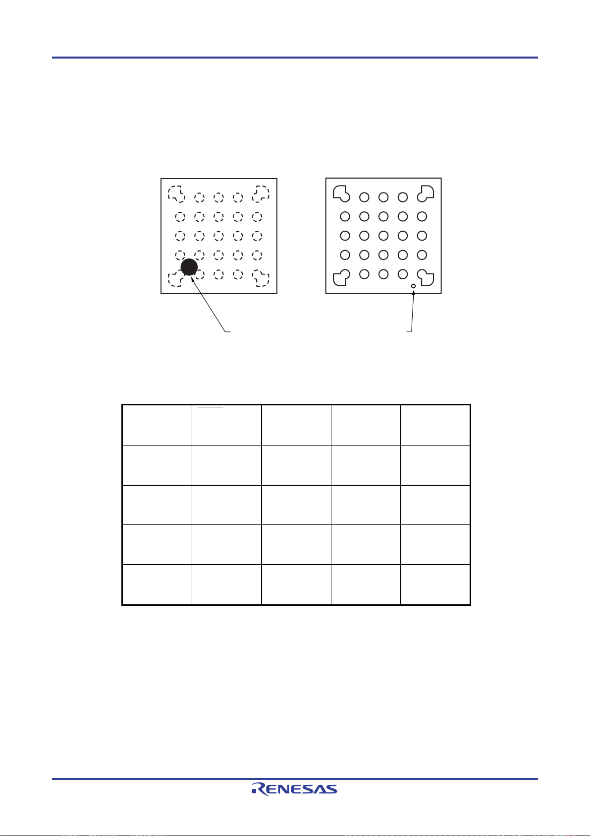
RL78/G1A CHAPTER 1 OUTLINE
1.3 Pin Configuration (Top View)
1.3.1 25-pin products
• 25-pin plastic WFLGA (3 × 3 mm, 0.50 mm pitch)
Top View
5
4
3
2
1
ABCDE EDCBA
Bottom View
INDEX MARK
INDEX MARK
A B C D E
SS
P40/TOOL0 RESET P03/ANI16/
5
P122/X2/
EXCLK
4
P121/X1 V
3
REGC
2
P60/SCLA0 P61/SDAA0 P31/ANI29/TI03/
1
A B C D E
P137/INTP0 P02/ANI17/
DD
SS P30/ANI27/
V
RxD1/TO00/
(KR1)
TxD1/TI00/
(KR0)
P21/ANI1/
REFM
AV
SCK11/SCL11/
INTP3
TO03/PCLBUZ0
/INTP4
P23/ANI3/
(KR3)
P22/ANI2/
(KR2)
P11/ANI20/
SI00/SDA00/
RxD0/
TOOLRxD
P51/ANI25/
SO11/INTP2
P12/ANI21/
SO00/TxD0/
TOOLTxD
AV
DD
AV
P10/ANI18/
SCK00/SCL00
P50/ANI26/
SI11/SDA11
INTP1
P20/ANI0/
REFP
AV
5
4
3
2
1
Caution Connect the REGC pin to Vss via a capacitor (0.47 to 1
μ
F).
Remarks 1. For pin identification, see 1.4 Pin Identification.
2. Functions in parentheses in the above figure can be assigned via settings in the peripheral I/O redirection
register (PIOR). See Figure 4-8 Format of Peripheral I/O Redirection Register (PIOR).
R01UH0305EJ0200 Rev.2.00 6
Jul 04, 2013
Page 27
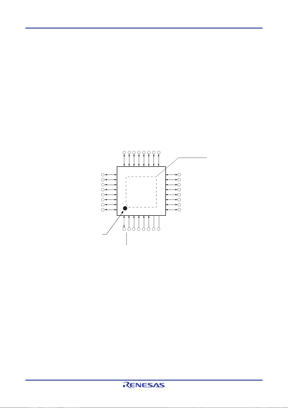
RL78/G1A CHAPTER 1 OUTLINE
1.3.2 32-pin products
• 32-pin plastic HWQFN (5 × 5 mm, 0.5 mm pitch)
<R>
P24/ANI4/(KR5)
P23/ANI3/(KR4)
P22/ANI2/(KR3)
P21/ANI1/AV
P20/ANI0/AV
P03/ANI16/RxD1/TO00/(KR2)
P02/ANI17/TxD1/TI00/(KR1)
P120/ANI19/(KR0)
INDEX MARK
REFM
REFP
AVSSAVDDP10/ANI18/SCK00/SCL00/(KR0)
24 23 22 21 20 19 18 17
25
26
27
28
29
30
31
32
1 2 3 4 5 6 7 8
P40/TOOL0
P11/ANI20/SI00/SDA00/RxD0/TOOLRxD/(KR1)
P12/ANI21/SO00/TxD0/TOOLTxD/(KR2)
P13/ANI22/SO20/TxD2/(KR3)
P14/ANI23/SI20/SDA20/RxD2/(KR4)
P15/ANI24/SCK20/SCL20/PCLBUZ1/(KR5)
exposed die pad
P51/SO11/INTP2
P50/ANI26/SI11/SDA11/INTP1
P30/ANI27/SCK11/SCL11/INTP3
P70/ANI28/KR0
P31/ANI29/TI03/TO03/PCLBUZ0/INTP4
P62
P61/SDAA0
P60/SCLA0
RESET
P121/X1
P137/INTP0
P122/X2/EXCLK
SS
V
REGC
16
15
14
13
12
11
10
9
DD
V
Caution Connect the REGC pin to Vss via a capacitor (0.47 to 1
μ
F).
Remarks 1. For pin identification, see 1.4 Pin Identification.
2. Functions in parentheses in the above figure can be assigned via settings in the peripheral I/O redirection
register (PIOR). See Figure 4-8 Format of Peripheral I/O Redirection Register (PIOR).
3. It is recommended to connect an exposed die pad to V
ss.
R01UH0305EJ0200 Rev.2.00 7
Jul 04, 2013
Page 28
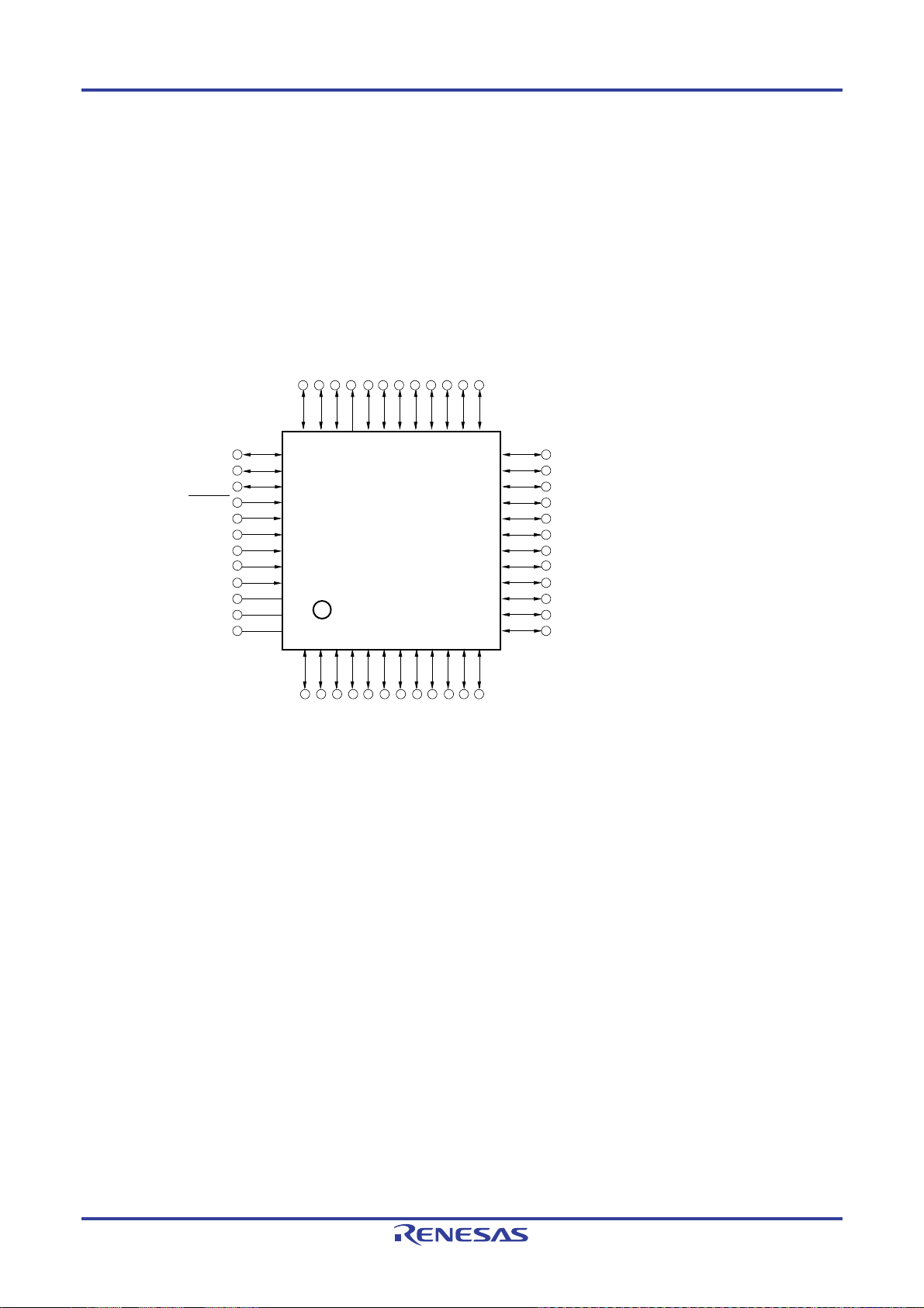
RL78/G1A CHAPTER 1 OUTLINE
1.3.3 48-pin products
• 48-pin plastic LFQFP (7 × 7 mm, 0.5 mm pitch)
REFP
REFM
P140/PCLBUZ0/INTP6
P02/ANI17/TxD1/TI00/(KR0)
P03/ANI16/RxD1/TO00/(KR1)
P130
P20/ANI0/AV
P21/ANI1/AV
P22/ANI2/(KR2)
P23/ANI3/(KR3)
P24/ANI4/(KR4)
P25/ANI5/(KR5)
P26/ANI6
P27/ANI7
P120/ANI19
P41/ANI30/TI07/TO07
P40/TOOL0
RESET
P124/XT2/EXCLKS
P123/XT1
P137/INTP0
P122/X2/EXCLK
P121/X1
REGC
V
V
36 35 34 33 32 31 30 29 28 27 26 25
37
38
39
40
41
42
43
44
45
46
SS
DD
47
48
1 2 3 4 5 6 7 8 9 10 11 12
P62
P63
P60/SCLA0
P61/SDAA0
P73/SO01/KR3
24
23
22
21
20
19
18
17
16
15
14
13
P72/SO21/KR2
AV
SS
AV
DD
P150/ANI8
P10/ANI18/SCK00/SCL00/(KR0)
P11/ANI20/SI00/SDA00/RxD0/TOOLRxD/(KR1)
P12/ANI21/SO00/TxD0/TOOLTxD/(KR2)
P13/ANI22/SO20/TxD2/(KR3)
P14/ANI23/SI20/SDA20/RxD2/(KR4)
P15/ANI24/SCK20/SCL20/PCLBUZ1/(KR5)
P16/TI01/TO01/INTP5
P51/ANI25/SO11/INTP2
P50/ANI26/SI11/SDA11/INTP1
P71/SI21/SDA21/KR1
P74/SI01/SDA01/INTP8/KR4
P31/ANI29/TI03/TO03/INTP4
P75/SCK01/SCL01/INTP9/KR5
P70/ANI28/SCK21/SCL21/KR0
P30/ANI27/SCK11/SCL11/INTP3/RTC1HZ
Caution Connect the REGC pin to Vss via a capacitor (0.47 to 1 μF).
Remarks 1. For pin identification, see 1.4 Pin Identification.
2. Functions in parentheses in the above figure can be assigned via settings in the peripheral I/O redirection
register (PIOR). See Figure 4-8 Format of Peripheral I/O Redirection Register (PIOR).
R01UH0305EJ0200 Rev.2.00 8
Jul 04, 2013
Page 29
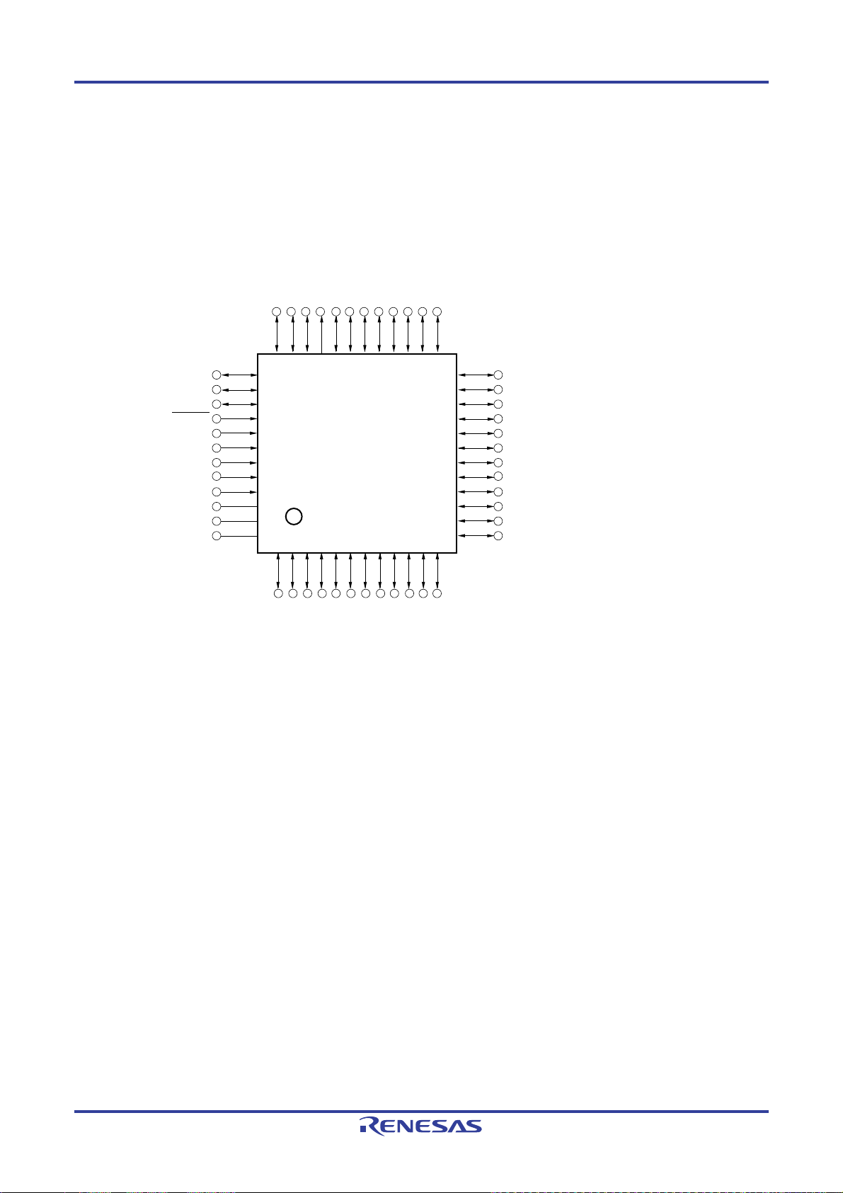
RL78/G1A CHAPTER 1 OUTLINE
• 48-pin plastic HWQFN (7 × 7 mm, 0.5 mm pitch)
REFP
REFM
P140/PCLBUZ0/INTP6
P02/ANI17/TxD1/TI00/(KR0)
P03/ANI16/RxD1/TO00/(KR1)
P130
P20/ANI0/AV
P21/ANI1/AV
P22/ANI2/(KR2)
P23/ANI3/(KR3)
P24/ANI4/(KR4)
P25/ANI5/(KR5)
P26/ANI6
P27/ANI7
P120/ANI19
P41/ANI30/TI07/TO07
P40/TOOL0
RESET
P124/XT2/EXCLKS
P123/XT1
P137/INTP0
P122/X2/EXCLK
P121/X1
REGC
V
V
36 35 34 33 32 31 30 29 28 27 26 25
37
38
39
40
41
42
43
44
45
46
SS
DD
47
48
1 2 3 4 5 6 7 8 9 10 11 12
P62
P63
P60/SCLA0
P61/SDAA0
P73/SO01/KR3
24
23
22
21
20
19
18
17
16
15
14
13
P72/SO21/KR2
AV
SS
AV
DD
P150/ANI8
P10/ANI18/SCK00/SCL00/(KR0)
P11/ANI20/SI00/SDA00/RxD0/TOOLRxD/(KR1)
P12/ANI21/SO00/TxD0/TOOLTxD/(KR2)
P13/ANI22/SO20/TxD2/(KR3)
P14/ANI23/SI20/SDA20/RxD2/(KR4)
P15/ANI24/SCK20/SCL20/PCLBUZ1/(KR5)
P16/TI01/TO01/INTP5
P51/ANI25/SO11/INTP2
P50/ANI26/SI11/SDA11/INTP1
P71/SI21/SDA21/KR1
P74/SI01/SDA01/INTP8/KR4
P31/ANI29/TI03/TO03/INTP4
P75/SCK01/SCL01/INTP9/KR5
P70/ANI28/SCK21/SCL21/KR0
P30/ANI27/SCK11/SCL11/INTP3/RTC1HZ
Caution Connect the REGC pin to Vss via a capacitor (0.47 to 1 μF).
Remarks 1. For pin identification, see 1.4 Pin Identification.
2. Functions in parentheses in the above figure can be assigned via settings in the peripheral I/O redirection
register (PIOR). See Figure 4-8 Format of Peripheral I/O Redirection Register (PIOR).
R01UH0305EJ0200 Rev.2.00 9
Jul 04, 2013
Page 30
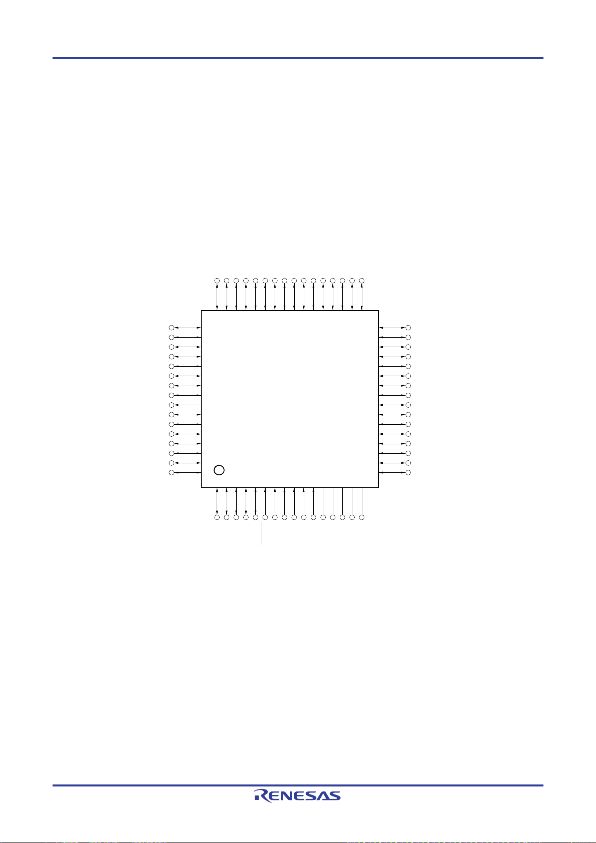
RL78/G1A CHAPTER 1 OUTLINE
1.3.4 64-pin products
• 64-pin plastic LFQFP (10 × 10 mm, 0.5 mm pitch)
P27/ANI7
P26/ANI6/(KR9)
P25/ANI5/(KR8)
P24/ANI4/(KR7)
P23/ANI3/(KR6)
P22/ANI2/(KR5)
P21/ANI1/AV
P20/ANI0/AV
P04/SCK10/SCL10/(KR4)
P03/ANI16/SI10/SDA10/RxD1/(KR3)
P02/ANI17/SO10/TxD1/(KR2)
P01/TO00/(KR1)
P00/TI00/(KR0)
P141/PCLBUZ1/INTP7
P140/PCLBUZ0/INTP6
REFM
REFP
P130
AVSSAVDDP150/ANI8
48 47 46 45 44 43 42 41 40 39 38 37 36 35 34 33
49
50
51
52
53
54
55
56
57
58
59
60
61
62
63
64
1 2 3 4 5 6 7 8 9 10 11 12 13 14 15 16
P120/ANI19
P151/ANI9/(KR6)
P152/ANI10/(KR7)
P153/ANI11/(KR8)
P43
RESET
P40/TOOL0
P42/TI04/TO04
P41/ANI30/TI07/TO07
P154/ANI12/(KR9)
P10/ANI18/SCK00/SCL00/(KR0)
P11/ANI20/SI00/SDA00/RxD0/TOOLRxD/(KR1)
P12/ANI21/SO00/TxD0/TOOLTxD/(KR2)
P13/ANI22/SO20/TxD2/(KR3)
P14/ANI23/SI20/SDA20/RxD2/(KR4)
P15/ANI24/SCK20/SCL20/(KR5)
P16/TI01/TO01/INTP5
P51/ANI25/SO11/INTP2
P50/ANI26/SI11/SDA11/INTP1
32
31
30
29
28
27
26
25
24
23
22
21
20
19
18
17
SS
DD
SS0
DD0
V
V
EV
REGC
P121/X1
P123/XT1
P137/INTP0
P122/X2/EXCLK
P124/XT2/EXCLKS
EV
P30/ANI27/SCK11/SCL11/INTP3/RTC1HZ
P05/TI05/TO05/KR8
P06/TI06/TO06/KR9
P70/ANI28/SCK21/SCL21/KR0
P71/SI21/SDA21/KR1
P72/SO21/KR2
P73/SO01/KR3
P74/SI01/SDA01/INTP8/KR4
P75/SCK01/SCL01/INTP9/KR5
P76/INTP10/KR6
P77/INTP11/KR7
P31/ANI29/TI03/TO03/INTP4
P63
P62
P61/SDAA0
P60/SCLA0
Cautions 1. Make EVSS0 pin the same potential as VSS pin.
2. Make VDD pin the potential that is higher than EVDD0 pin.
3. Connect the REGC pin to Vss via a capacitor (0.47 to 1
μ
F).
Remarks 1. For pin identification, see 1.4 Pin Identification.
2. When using the microcontroller for an application where the noise generated inside the microcontroller
must be reduced, it is recommended to supply separate powers to the V
the V
SS and EVSS0pins to separate ground lines.
DD and EVDD0 pins and connect
3. Functions in parentheses in the above figure can be assigned via settings in the peripheral I/O redirection
register (PIOR). See Figure 4-8 Format of Peripheral I/O Redirection Register (PIOR).
R01UH0305EJ0200 Rev.2.00 10
Jul 04, 2013
Page 31

RL78/G1A CHAPTER 1 OUTLINE
• 64-pin plastic VFBGA (4 × 4 mm, 0.4 mm pitch)
Top View Bottom View
8
7
6
5
4
3
2
1
ABCDEFGH
Index mark
HGFEDCBA
Pin No.
A1 P05/TI05/TO05/KR8 C1 P51/ANI25/SO11
A2 P30/ANI27/SCK11
/SCL11/INTP3
/RTC1HZ
A3 P70/ANI28/SCK21
/SCL21/KR0
A4 P75/SCK01/SCL01
/INTP9/KR5
A5 P77/INTP11/KR7 C5 P15/ANI24/SCK20
A6 P61/SDAA0 C6 P63 E6 P41/ANI30/TI07/TO07 G6 P02/ANI17/SO10/TxD1
A7 P60/SCLA0 C7 VSS E7 RESET G7 P00/TI00/(KR0)
A8 EVDD0 C8 P121/X1 E8 P137/INTP0 G8 P124/XT2/EXCLKS
B1 P50/ANI26 /SI11
/SDA11/INTP1
B2 P72/SO21/KR2 D2 P06/TI06/TO06/KR9 F2 P151/ANI9/(KR6) H2 P27/ANI7
B3 P73/SO01/KR3 D3 P12/ANI21/SO00
B4 P76/INTP10/KR6 D4 P14/ANI23/SI20/
B5 P31/ANI29/TI03/TO03
/INTP4
B6 P62 D6 P40/TOOL0 F6 P43 H6 P141/PCLBUZ1/INTP7
B7 VDD D7 REGC F7 P01/TO00/(KR1) H7 P140/PCLBUZ0/INTP6
B8 EVSS0 D8 P122/X2/EXCLK F8 P123/XT1 H8 P120/ANI19
Name Pin No.
C2 P71/SI21/SDA21/KR1 E2 P154/ANI12/(KR9) G2 P25/ANI5/(KR8)
C3 P74/SI01/SDA01
C4 P16/TI01/TO01/INTP5 E4 P11/ANI20/SI00
D1 P13/ANI22/SO20
D5 P42/TI04/TO04 F5 P04/SCK10/SCL10
/INTP2
/INTP8/KR4
/SCL20/(KR5)
/TxD2/(KR3)
/TxD0/TOOLTxD/(KR2)
SDA20/RxD2/(KR4)
Name Pin No. Name Pin No.
E1 P153/ANI11/(KR8) G1 AVDD
E3 P10/ANI18/SCK00
/SCL00/(KR0)
/SDA00/RxD0
/TOOLRxD/(KR1)
E5 P03/ANI16/SI10
/SDA10/RxD1/(KR3)
F1 P150/ANI8 H1 AVSS
F3 P152/ANI10/(KR7) H3 P26/ANI6/(KR9)
F4 P21/ANI1/AVREFM H4 P23/ANI3/(KR6)
/(KR4)
G3 P24/ANI4/(KR7)
G4 P22/ANI2/(KR5)
G5 P130
/(KR2)
H5 P20/ANI0/AVREFP
Name
Cautions 1. Make EVSS0 pin the same potential as VSS pin.
2. Make V
DD pin the potential that is higher than EVDD0 pin.
3. Connect the REGC pin to Vss via a capacitor (0.47 to 1 μF).
Remarks 1. For pin identification, see 1.4 Pin Identification.
2. When using the microcontroller for an application where the noise generated inside the microcontroller
must be reduced, it is recommended to supply separate powers to the V
the V
SS and EVSS0 pins to separate ground lines.
DD and EVDD0 pins and connect
3. Functions in parentheses in the above figure can be assigned via settings in the peripheral I/O
redirection register (PIOR). See Figure 4-8 Format of Peripheral I/O Redirection Register (PIOR).
R01UH0305EJ0200 Rev.2.00 11
Jul 04, 2013
Page 32

RL78/G1A CHAPTER 1 OUTLINE
1.4 Pin Identification
ANI0 to ANI12,
ANI16 to ANI30: Analog input
AV
DD: Analog power supply
AV
SS: Analog ground
AV
REFM: A/D converter reference
potential (− side) input
AV
REFP: A/D converter reference
potential (+ side) input
EV
DD0: Power supply for port
EV
SS0: Ground for port
EXCLK: External clock input (main
system clock)
EXCLKS: External clock input
(subsystem clock)
INTP0 to INTP11: Interrupt Request from
External
KR0 to KR9: Key return
P00 to P06: Port 0
P10 to P16: Port 1
P20 to P27: Port 2
P30, P31: Port 3
P40 to P43: Port 4
P50, P51: Port 5
P60 to P63: Port 6
P70 to P77: Port 7
P120 to P124: Port 12
P130, P137: Port 13
P140, P141: Port 14
P150 to P154: Port 15
PCLBUZ0, PCLBUZ1: Programmable clock output/buzzer
output
REGC: Regulator capacitance
RESET: Reset
RTC1HZ: Real-time clock correction clock
(1 Hz) output
RxD0 to RxD2: Receive data
SCK00, SCK01, SCK10,
SCK11, SCK20, SCK21: Serial clock input/output
SCLA0, SCL00, SCL01,
SCL10, SCL11, SCL20,
SCL21: Serial clock output
SDAA0, SDA00, SDA01,
SDA10, SDA11, SDA20,
SDA21: Serial data input/output
SI00, SI01, SI10, SI11,
SI20, SI21: Serial data input
SO00, SO01, SO10,
SO11, SO20, SO21: Serial data output
TI00, TI01, TI03 to TI07: Timer input
TO00, TO01,
TO03 to TO07: Timer output
TOOL0: Data input/output for tool
TOOLRxD, TOOLTxD: Data input/output for external device
TxD0 to TxD2: Transmit data
V
DD: Power supply
VSS: Ground
X1, X2: Crystal oscillator (main system clock)
XT1, XT2: Crystal oscillator (subsystem clock)
R01UH0305EJ0200 Rev.2.00 12
Jul 04, 2013
Page 33

RL78/G1A CHAPTER 1 OUTLINE
1.5 Block Diagram
1.5.1 25-pin products
TI00/P02
TO00/P03
TI03/TO03/P31
TIMER ARRAY
UNIT (8ch)
ch0
ch1
ch2
ch3
ch4
ch5
ch6
PORT 0
PORT 1
PORT 2
PORT 3
PORT 4
PORT 5
PORT 6
2
3
4
2
2
2
P02, P03
P10 to P12
P20 to P23
P30, P31
P40
P50, P51
P60, P61
LOW-SPEED
ON-CHIP
OSCILLATOR
RxD0/P11
TxD0/P12
RxD1/P03
TxD1/P02
SCK00/P10
SI00/P11
SO00/P12
SCK11/P30
SI11/P50
SO11/P51
SCL00/P10
SDA00/P11
SCL11/P30
SDA11/P50
ch7
WINDOW
WATCHDOG
TIMER
INTERVAL
TIMER
REAL-TIME
CLOCK
SERIAL ARRAY
UNIT0 (4ch)
UART0
UART1
CSI00
CSI11
IIC00
IIC11
DIRECT MEMORY
ACCESS
CONTROL
BCD
ADJUSTMENT
RL78
CPU
CORE
RAM
AV
SERIAL
INTERFACE IICA0
BUZZER OUTPUT
CLOCK OUTPUT
CONTROL
MULTIPLIER&
DIVIDER,
MULITIPLY-
ACCUMULATOR
CODE FLASH MEMORY
DATA FLASH MEMORY
V
SS
DD
TOOLRxD/P11,
TOOLTxD/P12
AV
SS
SDAA0/P61
SCLA0/P60
PCLBUZ0/P31
CRC
V
DD
PORT 12
PORT 13
(KEY RETURN)
A/D CONVERTER
POWER ON RESET/
VOLTAGE
DETECTOR
RESET CONTROL
ON-CHIP DEBUG
SYSTEM
CONTROL
HIGH-SPEED
ON-CHIP
OSCILLATOR
VOLTAGE
REGULATOR
INTERRUPT
CONTROL
P121, P122
2
P137
(KR0/P02, KR1/P03,
(4)
KR2/P22, KR3/P23)
ANI0/P20 to
4
ANI3/P23
ANI16/P03, ANI17/P02,
9
ANI18/P10, ANI20/P11,
ANI21/P12, ANI25/P51,
ANI26/P50, ANI27/P30,
ANI29/P31
AV
REFP
/P20
REFM
/P21
AV
POR/LVD
CONTROL
TOOL0/P40
RESET
X1/P121
X2/EXCLK/P122
REGC
INTP0/P137
INTP1/P50
INTP2/P51
INTP3/P30,
2
INTP4/P31
Remark Functions in parentheses in the above figure can be assigned via settings in the peripheral I/O redirection
register (PIOR). See Figure 4-8 Format of Peripheral I/O Redirection Register (PIOR).
R01UH0305EJ0200 Rev.2.00 13
Jul 04, 2013
Page 34

RL78/G1A CHAPTER 1 OUTLINE
1.5.2 32-pin products
<R>
TI00/P02
TO00/P03
TI03/TO03/P31
TIMER ARRAY
UNIT (8ch)
ch0
ch1
ch2
ch3
ch4
ch5
ch6
PORT 0
PORT 1
PORT 2
PORT 3
PORT 4
PORT 5
PORT 6
2
6
5
2
2
3
P02, P03
P10 to P15
P20 to P24
P30, P31
P40
P50, P51
P60 to P62
RxD2/P14
LOW-SPEED
ON-CHIP
OSCILLATOR
RxD0/P11
TxD0/P12
RxD1/P03
TxD1/P02
SCK00/P10
SI00/P11
SO00/P12
SCK11/P30
SI11/P50
SO11/P51
SCL00/P10
SDA00/P11
SCL11/P30
SDA11/P50
RxD2/P14
TxD2/P13
SCK20/P15
SI20/P14
SO20/P13
SCL20/P15
SDA20/P14
ch7
WINDOW
WATCHDOG
TIMER
INTERVAL
TIMER
REAL-TIME
CLOCK
SERIAL ARRAY
UNIT0 (4ch)
UART0
UART1
CSI00
CSI11
IIC00
IIC11
SERIAL ARRAY
UNIT1 (2ch)
UART2
LINSEL
CSI20
IIC20
RL78
CPU
CORE
RAM
V
AV
SERIAL
INTERFACE IICA0
BUZZER OUTPUT
CLOCK OUTPUT
CONTROL
MULTIPLIER&
DIVIDER,
MULITIPLY-
ACCUMULATOR
DIRECT MEMORY
ACCESS
CONTROL
BCD
ADJUSTMENT
CODE FLASH MEMORY
DATA FLASH MEMORY
V
SS
,
DD
,
AV
SS
DD
SDAA0/P61
SCLA0/P60
PCLBUZ0/P31,
2
PCLBUZ1/P15
TOOLRxD/P11,
TOOLTxD/P12
CRC
PORT 7
PORT 12
PORT 13
KEY RETURN
A/D CONVERTER
POWER ON RESET/
VOLTAGE
DETECTOR
RESET CONTROL
ON-CHIP DEBUG
SYSTEM
CONTROL
HIGH-SPEED
ON-CHIP
OSCILLATOR
VOLTAGE
REGULATOR
INTERRUPT
CONTROL
P70
P120
P121, P122
2
P137
KR0/P70
(KR0/P10 to KR5/P15)
1(6)
(KR0/P120, KR1/P02, KR2/P03,
KR3/P22 to KR5/P24)
ANI0/P20 to
5
ANI4/P24
ANI16/P01, ANI17/P00, ANI18/P10,
13
ANI19/P120 to ANI24/P15, ANI26/P50,
ANI27/P30, ANI28/P70, ANI29/P31
AV
REFP
/P20
AV
REFM
/P21
POR/LVD
CONTROL
TOOL0/P40
RESET
X1/P121
X2/EXCLK/P122
REGC
RxD2/P14
INTP0/P137
INTP1/P50,
2
INTP2/P51
INTP3/P30,
2
INTP4/P31
Remark Functions in parentheses in the above figure can be assigned via settings in the peripheral I/O redirection
register (PIOR). See Figure 4-8 Format of Peripheral I/O Redirection Register (PIOR).
R01UH0305EJ0200 Rev.2.00 14
Jul 04, 2013
Page 35

RL78/G1A CHAPTER 1 OUTLINE
1.5.3 48-pin products
<R>
TI00/P02
TO00/P03
TI01/TO01/P16
TI03/TO03/P31
TI07/TO07/P41
RxD2/P14
LOW-SPEED
ON-CHIP
OSCILLATOR
RTC1HZ/P30
RxD0/P11
TxD0/P12
RxD1/P03
TxD1/P02
SCK00/P10
SI00/P11
SO00/P12
SCK01/P75
SI01/P74
SO01/P73
SCK11/P30
SI11/P50
SO11/P51
SCL00/P10
SDA00/P11
SCL01/P75
SDA01/P74
SCL11/P30
SDA11/P50
RxD2/P14
TxD2/P13
SCK20/P15
SI20/P14
SO20/P13
SCK21/P70
SI21/P71
SO21/P72
SCL20/P15
SDA20/P14
SCL21/P70
SDA21/P71
Remark Functions in parentheses in the above figure can be assigned via settings in the peripheral I/O redirection
TIMER ARRAY
UNIT (8ch)
ch0
ch1
ch2
ch3
ch4
ch5
ch6
ch7
WINDOW
WATCHDOG
TIMER
INTERVAL
TIMER
REAL-TIME
CLOCK
SERIAL ARRAY
UNIT0 (4ch)
UART0
UART1
CSI00
CSI01
CSI11
IIC00
IIC01
IIC11
SERIAL ARRAY
UNIT1 (2ch)
UART2
LINSEL
CSI20
CSI21
IIC20
IIC21
RL78
CPU
CORE
RAM
AV
SERIAL
INTERFACE IICA0
BUZZER OUTPUT
CLOCK OUTPUT
CONTROL
MULTIPLIER&
DIVIDER,
MULITIPLY-
ACCUMULATOR
DIRECT MEMORY
ACCESS
CONTROL
BCD
ADJUSTMENT
V
SS,
V
DD,
AV
SS
DD
2
CODE FLASH MEMORY
DATA FLASH MEMORY
TOOLRxD/P11,
TOOLTxD/P12
SDAA0/P61
SCLA0/P60
PCLBUZ0/P140,
PCLBUZ1/P15
CRC
PORT 0
PORT 1
PORT 2
PORT 3
PORT 4
PORT 5
PORT 6
PORT 7
PORT 12
PORT 13
PORT 14 P140
PORT 15
A/D CONVERTER
KEY RETURN
POWER ON RESET/
VOLTAGE
DETECTOR
RESET CONTROL
ON-CHIP DEBUG
SYSTEM
CONTROL
HIGH-SPEED
ON-CHIP
OSCILLATOR
VOLTAGE
REGULATOR
INTERRUPT
CONTROL
2
P02, P03
7
P10 to P16
8
P20 to P27
2
P30, P31
2
P40, P41
2
P50, P51
4
P60 to P63
6
P70 to P75
P120
4
P121 to P124
P130
P137
P150
9
ANI0/P20 to ANI7/P2, ANI8/P150
ANI16/P03, ANI17/P02, ANI18/P147,
ANI19/P120, ANI20/P11 to ANI24/P15,
15
ANI25, P51, ANI26/P50, P30/ANI27,
ANI28/P70, ANI29/P31, ANI30/P41
AV
REFP
/P20
REFM
/P21
AV
KR0/P70 to KR5/P75
6(6)
(KR0/P10 to KR5/P15)
(KR0/P02, KR1/P03, KR2/P22 to KR5/P25)
POR/LVD
CONTROL
TOOL0/P40
RESET
X1/P121
X2/EXCLK/P122
XT1/P123
XT2/EXCLKS/P124
REGC
RxD2/P14
INTP0/P137
INTP1/P50,
2
INTP2/P51
INTP3/P30,
2
INTP4/P31
INTP5/P16
INTP6/P140
INTP8/P74,
2
INTP9/P75
register (PIOR). See Figure 4-8 Format of Peripheral I/O Redirection Register (PIOR).
R01UH0305EJ0200 Rev.2.00 15
Jul 04, 2013
Page 36

RL78/G1A CHAPTER 1 OUTLINE
1.5.4 64-pin products
TI00/P00
TO00/P01
TI01/TO01/P16
TI03/TO03/P31
TI04/TO04/P42
TI05/TO05/P05
TI06/TO06/P06
TI07/TO07/P41
RxD2/P14
LOW-SPEED
ON-CHIP
OSCILLATOR
RTC1HZ/P30
RxD0/P11
TxD0/P12
RxD1/P03
TxD1/P02
SCK00/P10
SI00/P11
SO00/P12
SCK01/P75
SI01/P74
SO01/P73
SCK10/P04
SI10/P03
SO10/P02
SCK11/P30
SI11/P50
SO11/P51
SCL00/P10
SDA00/P11
SCL01/P75
SDA01/P74
SCL10/P04
SDA10/P03
SCL11/P30
SDA11/P50
RxD2/P14
TxD2/P13
SCK20/P15
SI20/P14
SO20/P13
SCK21/P70
SI21/P71
SO21/P72
SCL20/P15
SDA20/P14
SCL21/P70
SDA21/P71
TIMER ARRAY
UNIT (8ch)
ch0
ch1
ch2
ch3
ch4
ch5
ch6
ch7
WINDOW
WATCHDOG
TIMER
INTERVAL
TIMER
REAL-TIME
CLOCK
SERIAL ARRAY
UNIT0 (4ch)
UART0
UART1
CSI00
CSI01
CSI10
CSI11
IIC00
IIC01
IIC10
IIC11
SERIAL ARRAY
UNIT1 (2ch)
UART2
LINSEL
CSI20
CSI21
IIC20
IIC21
RL78
CPU
CORE
RAM
EV
AV
SERIAL
INTERFACE IICA0
BUZZER OUTPUT
CLOCK OUTPUT
CONTROL
MULTIPLIER&
DIVIDER,
MULITIPLY-
ACCUMULATOR
DIRECT MEMORY
ACCESS
CONTROL
BCD
ADJUSTMENT
SS,
V
V
DD,
EV
SS0,
DD0,
AV
SS
DD
2
CODE FLASH MEMORY
DATA FLASH MEMORY
TOOLRxD/P11,
TOOLTxD/P12
SDAA0/P61
SCLA0/P60
PCLBUZ0/P140,
PCLBUZ1/P141
CRC
PORT 0
PORT 1
PORT 2
PORT 3
PORT 4
PORT 5
PORT 6
PORT 7
PORT 12
PORT 13
PORT 14
PORT 15
A/D CONVERTER
KEY RETURN
POWER ON RESET/
VOLTAGE
DETECTOR
RESET CONTROL
ON-CHIP DEBUG
SYSTEM
CONTROL
HIGH-SPEED
ON-CHIP
OSCILLATOR
VOLTAGE
REGULATOR
INTERRUPT
CONTROL
Remark Functions in parentheses in the above figure can be assigned via settings in the peripheral I/O redirection
register (PIOR). See Figure 4-8 Format of Peripheral I/O Redirection Register (PIOR).
7
P00 to P06
7
P10 to P16
8
P20 to P27
2
P30, P31
4
P40 to P43
2
P50, P51
4
P60 to P63
8
P70 to P77
P120
4
P121 to P124
P130
P137
2
P140, P141
5
P150 to P154
ANI0/P20 to ANI7/P27,
13
ANI8/P150 to ANI12/P154
ANI16/P03, ANI17/P02, ANI18/P10,
ANI19/P120, ANI20/P11 to ANI24/P15,
15
ANI25//P51, ANI26/P50, ANI27/P30,
ANI28/P70ANI29/P31, ANI30/P41
AVREFP/P20
AVREFM/P21
KR0/P70 to KR7/P77, KR8/P05, KR9/P06
10 (10)
(KR0/P00 to KR4/P04, KR5/P22 to KR9/P26)
(KR0/P10 to KR5/P15, KR6/P151 to KR9/P154)
POR/LVD
CONTROL
TOOL0/P40
RESET
X1/P121
X2/EXCLK/P122
XT1/P123
XT2/EXCLKS/P124
REGC
RxD2/P14
INTP0/P137
INTP1/P50,
2
INTP2/P51
INTP3/P30,
2
INTP4/P31
INTP5/P16
INTP6/P140,
2
INTP7/P141
INTP8/P74,
2
INTP9/P75
INTP10/P76,
2
INTP11/P77
R01UH0305EJ0200 Rev.2.00 16
Jul 04, 2013
Page 37

RL78/G1A CHAPTER 1 OUTLINE
1.6 Outline of Functions
25-pin 32-pin 48-pin 64-pin Item
R5F10E8x R5F10EBx R5F10EGx R5F10ELx
Code flash memory (KB) 16 to 64 16 to 64 16 to 64 32 to 64
Data flash memory (KB) 4 4 4 4
RAM (KB) 2 to 4
Address space 1 MB
Main system
clock
High-speed system
clock
High-speed on-chip
oscillator
X1 (crystal/ceramic) oscillation, external main system clock input (EXCLK)
1 to 20 MHz: V
HS (High-speed main) mode : 1 to 32 MHz (V
HS (High-speed main) mode : 1 to 16 MHz (V
LS (Low-speed main) mode : 1 to 8 MHz (VDD = 1.8 to 3.6 V),
LV (Low-voltage main) mode : 1 to 4 MHz (V
Subsystem clock XT1 (crystal) oscillation, external subsystem
Low-speed on-chip oscillator 15 kHz (TYP.)
(8-bit register × 8) × 4 bank General-purpose register
0.03125 μs (High-speed on-chip oscillator: fIH = 32 MHz operation) Minimum instruction execution time
0.05 μs (High-speed system clock: fMX = 20 MHz operation)
Instruction set
• Data transfer (8/16 bits)
• Adder and subtractor/logical operation (8/16 bits)
• Multiplication (8 bits × 8 bits)
• Rotate, barrel shift, and bit manipulation (Set, reset, test, and Boolean operation), etc.
Total 19 26 42 56 I/O port
<R>
CMOS I/O 14
(N-ch O.D. I/O [V
withstand voltage]: 6)
CMOS input 3 3 5 5
CMOS output 1 1
N-ch open-drain I/O
(6 V tolerance)
16-bit timer 8 channels Timer
Watchdog timer 1 channel
Real-time clock (RTC) 1 channel 1 channel
12-bit interval timer (IT) 1 channel
Timer output 2 channels (PWM outputs: 1 ) 4 channels
RTC output 1
Notes 1. In the case of the 4 KB, this is about 3 KB when the self-programming function and data flash function are
used. (For details, see CHAPTER 3)
<R>
2. Only the constant-period interrupt function when the low-speed on-chip oscillator clock (f
3. The number of PWM outputs varies depending on the setting of channels in use (the number of masters
and slaves). (6.9.3 Operation as multiple PWM output function).
Note1 Note1 Note1 Note1
DD = 2.7 to 3.6 V, 1 to 8 MHz: VDD = 1.8 to 2.7 V, 1 to 4 MHz: VDD = 1.6 to 1.8 V
2 to 4 2 to 4 2 to 4
DD = 2.7 to 3.6 V),
DD = 2.4 to 3.6 V),
DD = 1.6 to 3.6 V)
−
clock input (EXCLKS) 32.768 kHz (TYP.)
μ
s (Subsystem clock: fSUB = 32.768 kHz
−
30.5
operation)
(N-ch O.D. I/O [V
DD
withstand voltage]: 9)
20
DD
withstand voltage]: 11)
32
(N-ch O.D. I/O [V
(N-ch O.D. I/O [V
DD
withstand voltage]: 12)
46
− −
2 3 4 4
Note 2
Note 3
(PWM outputs: 3
7 channels
Note 3 Note 3
) )
(PWM outputs: 6
−
• 1 Hz (subsystem clock: f
SUB = 32.768 kHz)
IL) is selected.
(1/2)
DD
R01UH0305EJ0200 Rev.2.00 17
Jul 04, 2013
Page 38

RL78/G1A CHAPTER 1 OUTLINE
(2/2)
25-pin 32-pin 48-pin 64-pin Item
R5F10E8x R5F10EBx R5F10EGx R5F10ELx
1 2 2 2 Clock output/buzzer output
• 2.44 kHz, 4.88 kHz, 9.76 kHz, 1.25 MHz,
2.5 MHz, 5 MHz, 10 MHz
(Main system clock: f
MAIN = 20 MHz operation)
8/12-bit resolution A/D converter 13 channels 18 channels 24 channels 28 channels
Serial interface [25-pin products]
2
• CSI: 1 channel/simplified I
• CSI: 1 channel/simplified I
C: 1 channel/UART: 1 channel
2
C: 1 channel/UART: 1 channel
[32-pin products]
• CSI: 1 channel/simplified I
• CSI: 1 channel/simplified I
• CSI: 1 channel/simplified I
2
C: 1 channel/UART: 1 channel
2
C: 1 channel/UART: 1 channel
2
C: 1 channel/UART (UART supporting LIN-bus): 1 channel
[48-pin products]
2
• CSI: 2 channels/simplified I
• CSI: 1 channel/simplified I
• CSI: 2 channels/simplified I
C: 2 channels/UART: 1 channel
2
C: 1 channel/UART: 1 channel
2
C: 2 channels/UART (UART supporting LIN-bus): 1 channel
[64-pin products]
2
C: 2 channels/UART: 1 channel
2
C: 2 channels/UART: 1 channel
2
C: 2 channels/UART (UART supporting LIN-bus): 1 channel
I
2
C bus 1 channel 1 channel 1 channel 1 channel
Multiplier and divider/multiplyaccumulator
• CSI: 2 channels/simplified I
• CSI: 2 channels/simplified I
• CSI: 2 channels/simplified I
• 16 bits × 16 bits = 32 bits (Unsigned or signed)
• 32 bits ÷ 32 bits = 32 bits (Unsigned)
• 16 bits × 16 bits + 32 bits = 32 bits (Unsigned or signed)
DMA controller 2 channels
Internal 24 27 27 27 Vectored interrupt
sources
Key interrupt 0 ch (4 ch) 1 ch (6 ch)
Reset
External 6 6 10 13
Note 1
Note 1
• Reset by RESET pin
• Internal reset by watchdog timer
• Internal reset by power-on-reset
• Internal reset by voltage detector
• Internal reset by illegal instruction execution
• Internal reset by RAM parity error
• Internal reset by illegal-memory access
Power-on-reset circuit • Power-on-reset: 1.51 V (TYP.)
• Power-down-reset: 1.50 V (TYP.)
Voltage detector
• Rising edge : 1.67 V to 3.14 V (12 stages)
• Falling edge : 1.63 V to 3.06 V (12 stages)
On-chip debug function Provided
Power supply voltage VDD = 1.6 to 3.6 V
TA = −40 to +85°C (A: Consumer application), TA = −40 to +105°C (G: Industrial application) Operating ambient temperature
Notes 1. Can be used by the Peripheral I/O redirection register (PIOR).
2. The illegal instruction is generated when instruction code FFH is executed.
Reset by the illegal instruction execution not issued by emulation with the in-circuit emulator or on-chip
debug emulator.
• 2.44 kHz, 4.88 kHz, 9.76 kHz, 1.25 MHz,
2.5 MHz, 5 MHz, 10 MHz
(Main system clock: f
MAIN = 20 MHz operation)
• 256 Hz, 512 Hz, 1.024 kHz, 2.048 kHz,
4.096 kHz, 8.192 kHz, 16.384 kHz, 32.768 kHz
(Subsystem clock: f
SUB = 32.768 kHz operation)
6 ch 10 ch
Note 2
R01UH0305EJ0200 Rev.2.00 18
Jul 04, 2013
Page 39

RL78/G1A CHAPTER 2 PIN FUNCTIONS
CHAPTER 2 PIN FUNCTIONS
2.1 Port Function
Pin I/O buffer power supplies depend on the product. The relationship between these power supplies and the pins is
shown below.
Table 2-1. Pin I/O Buffer Power Supplies
(1) 25-pin products
Power Supply Corresponding Pins
VDD Port pins other than P20 to P23
• RESET, REGC
AVDD • P20 to P23
(2) 32-pin products
Power Supply Corresponding Pins
VDD Port pins other than P20 to P24
• RESET, REGC
AVDD • P20 to P24
(3) 48-pin products
Power Supply Corresponding Pins
VDD Port pins other than P20 to P27, P150
• RESET, REGC
AVDD • P20 to P27, P150
(4) 64-pin products
Power Supply Corresponding Pins
EVDD0 Port pins other than P20 to P27, P121 to P124, P137, and P150 to P154
VDD • P121 to P124, P137
• RESET, REGC
AVDD • P20 to P27, and P150 to P154
R01UH0305EJ0200 Rev.2.00 19
Jul 04, 2013
Page 40

RL78/G1A CHAPTER 2 PIN FUNCTIONS
Set in each port I/O, buffer, pull-up resistor is also valid for alternate functions.
2.1.1 25-pin products
<R>
Function
Name
P02 7-3-2
P03 8-3-2
P10
P11
P12 7-3-2
P20 ANI0/AVREFP
P21 ANI1/AVREFM
P22 ANI2/(KR2)
P23
P30 ANI27/INTP3/
P31
P40 7-1-1 I/O Input port TOOL0
P50 7-3-2 ANI26/INTP1/SI11/
P51 7-3-1
P60
P61
Notes 1. Digital or analog for each pin can be selected with the port mode control register x (PMCx) (can be set in 1-
2. Digital or analog for each pin can be selected with the A/D port configuration register (ADPC).
Remark Functions in parentheses in the above figure can be assigned via settings in the peripheral I/O redirection
Pin
I/O After Reset Alternate Function Function
Type
I/O Analog input port
ANI17/TI00/TxD1/
(KR0)
ANI16/TO00/RxD1/
(KR1)
Port 0.
2-bit I/O port.
Input/output can be specified in 1-bit units.
Use of an on-chip pull-up resistor can be specified by a
software setting at input port.
Input of P03 can be set to TTL input buffer.
Output of P02 and P03 can be set to N-ch open-drain
DD tolerance).
Note 1
.
8-3-2
I/O Analog input port
ANI18/SCK00/SCL00
ANI20/SI00/RxD0/
TOOLRxD/SDA00
ANI21/SO00/TxD0/
TOOLTxD
output (V
Can be set to analog input
Port 1.
3-bit I/O port.
Input/output can be specified in 1-bit units.
Use of an on-chip pull-up resistor can be specified by a
software setting at input port.
Input of P10 and P11 can be set to TTL input buffer.
Output of P10 to P12 can be set to N-ch open-drain
DD tolerance).
Note 1
.
4-3-1 I/O Analog input port
output (V
Can be set to analog input
Port 2.
4-bit I/O port.
Input/output can be specified in 1-bit units.
Can be set to analog input
Note 2
.
ANI3/(KR3)
7-3-1 I/O Analog input port
SCK11/SCL11
ANI29/TI03/TO03/
INTP4/PCLBUZ0
Port 3.
2-bit I/O port.
Input/output can be specified in 1-bit units.
Use of an on-chip pull-up resistor can be specified by a
software setting at input port.
Can be set to analog input
Note 1
.
Port 4.
1-bit I/O port.
Input/output can be specified.
Use of an on-chip pull-up resistor can be specified by a
software setting at input port.
I/O Analog input port
SDA11
Port 5.
2-bit I/O port.
Input/output can be specified in 1-bit units.
Use of an on-chip pull-up resistor can be specified by a
ANI25/INTP2/SO11
software setting at input port.
Output of P50 can be set to N-ch open-drain output
DD tolerance).
12-1-1 I/O Input port
SCLA0
SDAA0
(V
Can be set to analog input
Port 6.
2-bit I/O port.
Input/output can be specified in 1-bit units.
Note 1
.
Output of P60 and P61 can be set to N-ch open-drain
output (6 V tolerance).
bit units).
register (PIOR). See Figure 4-8 Format of Peripheral I/O Redirection Register (PIOR).
(1/2)
R01UH0305EJ0200 Rev.2.00 20
Jul 04, 2013
Page 41

RL78/G1A CHAPTER 2 PIN FUNCTIONS
<R>
Function
Name
P121 X1
P122
P137 2-1-2 Input Input port INTP0 Port 13.
RESET 2-1-1 Input
Pin
Type
2-2-1 Input Input port
I/O After Reset Alternate Function Function
− −
X2/EXCLK
Port 12.
2-bit input only port.
1-bit input only port.
Input only pin for external reset
When external reset is not used, connect this pin to V
directly or via a resistor.
(2/2)
DD
R01UH0305EJ0200 Rev.2.00 21
Jul 04, 2013
Page 42

RL78/G1A CHAPTER 2 PIN FUNCTIONS
2.1.2 32-pin products
<R>
Function
Name
P02 7-3-2
P03 8-3-2
P10
P11
P12
P13
P14
P15
P20 ANI0/AVREFP
P21 ANI1/AVREFM
P22 ANI2/(KR3)
P23 ANI3/(KR4)
P24
P30 ANI27/INTP3/
P31
P40 7-1-1 I/O Input port TOOL0
Notes 1. Digital or analog for each pin can be selected with the port mode control register x (PMCx) (can be set in 1-
2. Digital or analog for each pin can be selected with the A/D port configuration register (ADPC).
Remark Functions in parentheses in the above figure can be assigned via settings in the peripheral I/O redirection
Pin
I/O After Reset Alternate Function Function
Type
I/O Analog input
port
ANI17/TI00/TxD1/
(KR1)
ANI16/TO00/RxD1/
(KR2)
Port 0.
2-bit I/O port.
Input/output can be specified in 1-bit units.
Use of an on-chip pull-up resistor can be specified by a
software setting at input port.
Input of P03 can be set to TTL input buffer.
Output of P02 and P03 can be set to N-ch open-drain
DD tolerance).
DD tolerance).
Note 1
.
8-3-2
I/O Analog input
port
7-3-2
8-3-2
ANI18/SCK00/
SCL00/(KR0)
ANI20/SI00/RxD0/
TOOLRxD/SDA00/
(KR1)
ANI21/SO00/TxD0/
TOOLTxD/(KR2)
ANI22/TxD2/SO20/
(KR3)
ANI23/RxD2/SI20/
output (V
Can be set to analog input
Port 1.
6-bit I/O port.
Input/output can be specified in 1-bit units.
Use of an on-chip pull-up resistor can be specified by a
software setting at input port.
Input of P10, P11, P14, and P15 can be set to TTL input
buffer.
Output of P10 to P15 can be set to N-ch open-drain
output (V
Can be set to analog input.
SDA20/(KR4)
ANI24/PCLBUZ1/
SCK20/SCL20/(KR5)
4-3-1 I/O Analog input
port
Port 2.
5-bit I/O port.
Input/output can be specified in 1-bit units.
Can be set to analog input
Note 2
.
ANI4/(KR5)
7-3-1 I/O Analog input
port
SCK11/SCL11
ANI29/TI03/TO03/
INTP4/PCLBUZ0
Port 3.
2-bit I/O port.
Input/output can be specified in 1-bit units.
Use of an on-chip pull-up resistor can be specified by a
software setting at input port.
Can be set to analog input
Note 1
.
Port 4.
1-bit I/O port.
Input/output can be specified in 1-bit units.
Use of an on-chip pull-up resistor can be specified by a
software setting at input port.
bit units.
register (PIOR). See Figure 4-8 Format of Peripheral I/O Redirection Register (PIOR).
(1/2)
R01UH0305EJ0200 Rev.2.00 22
Jul 04, 2013
Page 43

RL78/G1A CHAPTER 2 PIN FUNCTIONS
<R>
Function
Name
P50 7-3-2 Analog input port ANI26/INTP1/SI11/
P51 7-1-1
P60
P61
P62
P70 7-3-1 I/O Analog input port ANI28/KR0 Port 7.
P120 7-3-1 I/O Analog input port ANI19/(KR0)
P121 X1
P122
P137 2-1-2 Input Input port INTP0 Port 13
Pin Type I/O After Reset Alternate Function Function
I/O
SDA11
Input port INTP2/SO11
Port 5.
2-bit I/O port.
Input/output can be specified in 1-bit units.
Use of an on-chip pull-up resistor can be specified by a
software setting at input port.
Output of P50 can be set to N-ch open-drain output
DD tolerance).
12-1-1 I/O Input port
SCLA0
SDAA0
(V
P50 can be set to analog input
Port 6.
3-bit I/O port.
−
Input/output can be specified in 1-bit units.
Note
Output of P60 to P62 can be set to N-ch open-drain
output (6 V tolerance).
1-bit I/O port.
Input/output can be specified.
Use of an on-chip pull-up resistor can be specified by a
software setting at input port.
Can be set to analog input
Note
.
Port 12.
2-2-1 Input Input port
X2/EXCLK
1-bit I/O port and 2-bit input only port.
P120 can be set to analog input
For only P120, input/output can be specified.
For only P120, use of an on-chip pull-up resistor can be
specified by a software setting at input port.
1bit input only port.
Note
.
(2/2)
RESET 2-1-1 Input
− −
Input only pin for external reset
When external reset is not used, connect this pin to V
directly or via a resistor.
Note Digital or analog for each pin can be selected with the port mode control register x (PMCx) (can be set in 1-bit
units).
Remark Functions in parentheses in the above figure can be assigned via settings in the peripheral I/O redirection
register (PIOR). See Figure 4-8 Format of Peripheral I/O Redirection Register (PIOR).
DD
R01UH0305EJ0200 Rev.2.00 23
Jul 04, 2013
Page 44
RL78/G1A CHAPTER 2 PIN FUNCTIONS
2.1.3 48-pin products
<R>
Function
Name
P02 7-3-2
P03 8-3-2
P10
P11
P12
P13
P14
P15
P16 8-1-1
P20
P21
P22
P23
P24
P25
P26
P27
P30
P31
Notes 1. Digital or analog for each pin can be selected with the port mode control register x (PMCx) (can be set in 1-
2. Digital or analog for each pin can be selected with the A/D port configuration register (ADPC).
Remark Functions in parentheses in the above figure can be assigned via settings in the peripheral I/O redirection
Pin
I/O After Reset Alternate Function Function
Type
I/O Analog input port
ANI17/TI00/TxD1/
(KR0)
ANI16TO00/RxD1/
(KR1)
Port 0.
2-bit I/O port.
Input/output can be specified in 1-bit units.
Use of an on-chip pull-up resistor can be specified by a
software setting at input port.
Input of P03 can be set to TTL input buffer.
Output of P02 and P03 can be set to N-ch open-drain
DD tolerance).
DD tolerance).
Note 1
.
Note 1
8-3-2
7-3-2
8-3-2
I/O
Analog input port
ANI18/SCK00/
SCL00/(KR0)
ANI20/SI00/RxD0/
TOOLRxD/SDA00/
(KR1)
ANI21/SO00/TxD0/
TOOLTxD/(KR2)
ANI22/TxD2/SO20/
(KR3)
ANI23/RxD2/SI20/
output (V
Can be set to analog input
Port 1.
7-bit I/O port.
Input/output can be specified in 1-bit units.
Use of an on-chip pull-up resistor can be specified by a
software setting at input port.
Input of P10, P11, and P14 to P16 can be set to TTL
input buffer.
Output of P10 to P15 can be set to N-ch open-drain
output (V
P10 to P15 can be set to analog input
SDA20/(KR4)
ANI24/PCLBUZ1/
SCK20/SCL20/(KR5)
Input port
4-3-1 I/O Analog input port
TI01/TO01/INTP5
ANI0/AV
ANI1/AV
REFP
REFM
ANI2/(KR2)
Port 2.
8-bit I/O port.
Input/output can be specified in 1-bit units.
Can be set to analog input
Note 2
.
ANI3/(KR3)
ANI4/(KR4)
ANI5/(KR5)
ANI6
ANI7
7-3-1 I/O Analog input port
ANI27/INTP3/
RTC1HZ/SCK11/
SCL11
ANI29/TI03/TO03/
INTP4
Port 3.
2-bit I/O port.
Input/output can be specified in 1-bit units.
Use of an on-chip pull-up resistor can be specified by a
software setting at input port.
Can be set to analog input
Note 1
.
bit units).
register (PIOR). See Figure 4-8 Format of Peripheral I/O Redirection Register (PIOR).
.
(1/2)
R01UH0305EJ0200 Rev.2.00 24
Jul 04, 2013
Page 45

RL78/G1A CHAPTER 2 PIN FUNCTIONS
<R>
Function
Name
P40 7-1-1 Input port
P41 7-3-1
P50 7-3-2 ANI26/INTP1/SI11/
P51 7-3-1
P60
P61
P62
P63
P70 7-3-1 Analog input port
P71 7-1-2
P72
P73
P74 7-1-2
P75 7-1-1
P120 7-3-1 I/O Analog input port
P121
P122
P123
P124
P130 1-1-1 Output Output port
P137 2-1-2 Input Input port INTP0
P140 7-1-1 Input port
P150 4-3-1
RESET 2-1-1 Input
Notes 1. Digital or analog for each pin can be selected with the port mode control register x (PMCx) (can be set in 1-
2. Digital or analog for each pin can be selected with the A/D port configuration register (ADPC).
Pin
I/O After Reset Alternate Function Function
Type
I/O
Analog input port
I/O Analog input port
12-1-1 I/O Input port
I/O
Input port
7-1-1
2-2-1 Input Input port
I/O
Analog input port ANI18
− −
bit units).
TOOL0
ANI30/TI07/TO07
SDA11
ANI25/INTP2/SO11
SCLA0
SDAA0
−
−
ANI28/KR0/SCK21/
SCL21
KR1/SI21/SDA21
KR2/SO21
KR3/SO01
KR4/INTP8/SI01/
SDA01
KR5/INTP9/SCK01/
SCL01
ANI19
X1
X2/EXCLK
XT1
XT2/EXCLKS
−
PCLBUZ0/INTP6
Port 4.
2-bit I/O port.
Input/output can be specified in 1-bit units.
Use of an on-chip pull-up resistor can be specified by a
software setting at input port.
P41 can be set to analog input
Note 1
.
Port 5.
2-bit I/O port.
Input/output can be specified in 1-bit units.
Use of an on-chip pull-up resistor can be specified by a
software setting at input port.
Output of P50 can be set to N-ch open-drain output
DD tolerance).
(V
Can be set to analog input
Note 1
.
Port 6.
4-bit I/O port.
Input/output can be specified in 1-bit units.
N-ch open-drain output (6 V tolerance).
Port 7.
6-bit I/O port.
Input/output can be specified in 1-bit units.
Use of an on-chip pull-up resistor can be specified by a
software setting at input port.
Output of P71 and P74 can be set to N-ch open-drain
output (V
P70 can be set to analog input
DD tolerance).
Note 1
.
Port 12.
1-bit I/O port and 4-bit input only port.
For only P120, input/output can be specified.
For only P120, use of an on-chip pull-up resistor can be
specified by a software setting at input port.
P120 can be set to analog input
Note 1
.
Port 13.
1-bit output port and 1-bit input only port.
Port 14.
1-bit I/O port.
Input/output can be specified.
Use of an on-chip pull-up resistor can be specified by a
software setting at input port.
Port 15
1-bit I/O port.
Input/output can be specified.
Can be set to analog input
Note 2
.
Input only pin for external reset
When external reset is not used, connect this pin to V
directly or via a resistor.
(2/2)
DD
R01UH0305EJ0200 Rev.2.00 25
Jul 04, 2013
Page 46

RL78/G1A CHAPTER 2 PIN FUNCTIONS
2.1.4 64-pin products
<R>
Function
Name
P00 TI00/(KR0)
P01
P02 7-3-2 ANI17/SO10/TxD1/
P03 8-3-2
P04 8-1-2 SCK10/SCL10/(KR4)
P05 TI05/TO05/KR8
P06
P10
P11
P12 ANI21/SO00/TxD0/
P13
P14 ANI23/RxD2/SI20/
P15
P16 8-1-1
P20
P21
P22
P23
P24
P25
P26
P27
P30
P31
Notes 1. Digital or analog for each pin can be selected with the port mode control register x (PMCx) (can be set in 1-
2. Digital or analog for each pin can be selected with the A/D port configuration register (ADPC).
Remark Functions in parentheses in the above figure can be assigned via settings in the peripheral I/O redirection
Pin
I/O After Reset Alternate Function Function
Type
8-1-1 Input port
I/O
TO00/(KR1)
Analog input port
(KR2)
ANI16/SI10/RxD1/
SDA10/(KR3)
Input port
7-1-1
Port 0.
7-bit I/O port.
Input/output can be specified in 1-bit units.
Use of an on-chip pull-up resistor can be specified by a
software setting at input port.
Input of P00, P01, P03, and P04 can be set to TTL input
buffer.
Output of P02 to P04 can be set to N-ch open-drain
output (V
DD tolerance).
P02 and P03 can be set to analog input
TI06/TO06/KR9
8-3-2
7-3-2
I/O
Analog input port
ANI18/SCK00/
SCL00/(KR0)
ANI20/SI00/RxD0/
TOOLRxD/SDA00/
(KR1)
TOOLTxD/(KR2)
ANI22/TxD2/SO20/
(KR3)
Port 1.
7-bit I/O port.
Input/output can be specified in 1-bit units.
Use of an on-chip pull-up resistor can be specified by a
software setting at input port.
Input of P10, P11, and P14 to P16 can be set to TTL
input buffer.
Output of P10 to P15 can be set to N-ch open-drain
output (V
P10 to P15 can be set to analog input
DD tolerance).
Note 1
8-3-2
SDA20/(KR4)
ANI24/SCK20/
SCL20/(KR5)
Input port TI01/TO01/INTP5
4-3-1 I/O Analog input port
ANI0/AV
ANI1/AV
REFP
REFM
ANI2/(KR5)
Port 2.
8-bit I/O port.
Input/output can be specified in 1-bit units.
Can be set to analog input
Note 2
.
ANI3/(KR6)
ANI4/(KR7)
ANI5/(KR8)
ANI6/(KR9)
ANI7
7-3-2 I/O Analog input port
bit units).
ANI27/INTP3/
RTC1HZ/SCK11/
SCL11
ANI29/TI03/TO03/
INTP4
Port 3.
2-bit I/O port.
Input/output can be specified in 1-bit units.
Use of an on-chip pull-up resistor can be specified by a
software setting at input port.
Can be set to analog input
Note 1
.
register (PIOR). See Figure 4-8 Format of Peripheral I/O Redirection Register (PIOR).
Note 1
.
.
(1/3)
R01UH0305EJ0200 Rev.2.00 26
Jul 04, 2013
Page 47

RL78/G1A CHAPTER 2 PIN FUNCTIONS
<R>
Function
Name
P40 7-1-1 Input port TOOL0
P41 7-3-1 Analog input port ANI30/8TI07/TO07
P42 TI04/TO04
P43
P50 7-3-2 ANI26/INTP1/SI11/
P51 7-3-1
P60
P61
P62
P63
P70 7-3-1 Analog input port
P71 7-1-2
P72
P73
P74 7-1-2
P75
P76
P77
P120 7-3-1 I/O Analog input port
P121
P122
P123
P124
P130 1-1-1 Output Output port
P137 2-1-2 Input Input port INTP0
P140
P141
Note Digital or analog for each pin can be selected with the port mode control register x (PMCx) (can be set in 1-bit
Pin Type I/O After Reset Alternate Function Function
I/O
Port 4.
4-bit I/O port.
7-1-1
Input port
−
Input/output can be specified in 1-bit units.
Use of an on-chip pull-up resistor can be specified by a
software setting at input port.
P41 can be set to analog input
I/O Analog input port
SDA11
ANI25/INTP2/SO11
Port 5.
2-bit I/O port.
Input/output can be specified in 1-bit units.
Use of an on-chip pull-up resistor can be specified by a
software setting at input port.
Output of P50 can be set to N-ch open-drain output (V
tolerance).
Can be set to analog input
12-1-1 I/O Input port
I/O
Input port
7-1-1
7-1-1
SCLA0
SDAA0
−
−
ANI28/KR0/SCK21/
SCL21
KR1/SI21/SDA21
KR2/SO21
KR3/SO01
KR4/INTP8/SI01/
SDA01
KR5/INTP9/SCK01/
Port 6.
4-bit I/O port.
Input/output can be specified in 1-bit units.
N-ch open-drain output (6 V tolerance).
Port 7.
8-bit I/O port.
Input/output can be specified in 1-bit units.
Use of an on-chip pull-up resistor can be specified by a
software setting at input port.
Output of P71 and P74 can be set to N-ch open-drain
output (V
DD tolerance).
P70 can be set to analog input
SCL01
KR6/INTP10
KR7/INTP11
Port 12.
1-bit I/O port and 4-bit input only port.
For only P120, input/output can be specified.
For only P120, use of an on-chip pull-up resistor can be
specified by a software setting at input port.
P120 can be set to analog input
Port 13.
2-2-1 Input Input port
ANI19
X1
X2/EXCLK
XT1
XT2/EXCLKS
−
1-bit output port and 1-bit input only port.
7-1-1 I/O Input port
PCLBUZ0/INTP6
PCLBUZ1/INTP7
Port 14.
2-bit I/O port.
Input/output can be specified in 1-bit units.
Use of an on-chip pull-up resistor can be specified by a
software setting at input port.
units).
Note
Note
.
.
Note
.
Note
.
(2/3)
DD
R01UH0305EJ0200 Rev.2.00 27
Jul 04, 2013
Page 48

RL78/G1A CHAPTER 2 PIN FUNCTIONS
<R>
Function
Name
P150
P151
P152
P153
P154
RESET 2-1-1 Input
Note Digital or analog for each pin can be selected with the A/D port configuration register (ADPC).
Remark Functions in parentheses in the above figure can be assigned via settings in the peripheral I/O redirection
Pin Type I/O After Reset Alternate Function Function
4-3-1 I/O Analog input port
− −
ANI8
ANI9/(KR6)
ANI10/(KR7)
ANI11/(KR8)
ANI12/(KR9)
Port 15.
5-bit I/O port.
Input/output can be specified in 1-bit units.
Can be set to analog input
Input only pin for external reset
When external reset is not used, connect this pin to V
directly or via a resistor.
Note
.
register (PIOR). See Figure 4-8 Format of Peripheral I/O Redirection Register (PIOR).
(3/3)
DD
R01UH0305EJ0200 Rev.2.00 28
Jul 04, 2013
Page 49

RL78/G1A CHAPTER 2 PIN FUNCTIONS
2.2 Functions Other than Port Pins
2.2.1 With functions for each product
(1/4)
Function
Name
ANI0
ANI1
ANI2
ANI3
ANI4
ANI5
ANI6
ANI7
ANI8
ANI9
ANI10
ANI11
ANI12
ANI16
ANI17
ANI18
ANI19
ANI20
ANI21
ANI22
ANI23
ANI24
ANI25
ANI26
ANI27
ANI28
ANI29
ANI30
INTP0
INTP1
INTP2
INTP3
INTP4
INTP5
INTP6
INTP7
INTP8
INTP9
INTP10
INTP11
64-pin 48-pin 32-pin 25-pin
√ √ √ √
√ √ √ √
√ √ √ √
√ √ √ √
√ √ √ −
√ √ − −
√ √ − −
√ √ − −
√ √ − −
√ − − −
√ − − −
√ − − −
√ − − −
√ √ √ √
√ √ √ √
√ √ √ √
√ √ √ −
√ √ √ √
√ √ √ √
√ √ √ −
√ √ √ −
√ √ √ −
√ √ − √
√ √ √ √
√ √ √ √
√ √ √ −
√ √ √ √
√ √ − −
√ √ √ √
√ √ √ √
√ √ √ √
√ √ √ √
√ √ √ √
√ √ − −
√ √ − −
√ − − −
√ √ − −
√ √ − −
√ − − −
√ − − −
R01UH0305EJ0200 Rev.2.00 29
Jul 04, 2013
Page 50

RL78/G1A CHAPTER 2 PIN FUNCTIONS
(2/4)
Function
Name
KR0
KR1
KR2
KR3
KR4
KR5
KR6
KR7
KR8
KR9
PCLBUZ0
PCLBUZ1
REGC
RTC1HZ
RESET
RxD0
RxD1
RxD2
SCK00
SCK01
SCK10
SCK11
SCK20
SCK21
SCLA0
SCL00
SCL01
SCL10
SCL11
SCL20
SCL21
SDAA0
SDA00
SDA01
SDA10
SDA11
SDA20
SDA21
64-pin 48-pin 32-pin 25-pin
√ √ √
√ √
√ √
√ √
√ √
√ √
√ − − −
√ − − −
√ − − −
√ − − −
√ √ √ √
√ √ √ −
√ √ √ √
√ √ − −
√ √ √ √
√ √ √ √
√ √ √ √
√ √ √ −
√ √ √ √
√ √ − −
√ − − −
√ √ √ √
√ √ √ −
√ √ − −
√ √ √ √
√ √ √ √
√ √ − −
√ − − −
√ √ √ √
√ √ √ −
√ √ − −
√ √ √ √
√ √ √ √
√ √ − −
√ − − −
√ √ √ √
√ √ √ −
√ √ − −
(√) (√)
(√) (√)
(√) (√)
(√)
(√)
(√)
−
−
Remark The checked function is available only when the bit corresponding to the function in the peripheral I/O
redirection register (PIOR) is set to 1.
R01UH0305EJ0200 Rev.2.00 30
Jul 04, 2013
Page 51

RL78/G1A CHAPTER 2 PIN FUNCTIONS
(3/4)
Function
Name
SI00
SI01
SI10
SI11
SI20
SI21
SO00
SO01
SO10
SO11
SO20
SO21
TI01
TI03
TI04
TI05
TI06
TI07
TO00
TO01
TO03
TO04
TO05
TO06
TO07
TxD0
TxD1
TxD2
X1
X2
EXCLK
EXCLKS
TI00
XT1
XT2
64-pin 48-pin 32-pin 25-pin
√ √ √ √
√ √ − −
√ − − −
√ √ √ √
√ √ √ −
√ √ − −
√ √ √ √
√ √ − −
√ − − −
√ √ √ √
√ √ √ −
√ √ − −
√ √ − −
√ √ √ √
√ − − −
√ − − −
√ − − −
√ √ − −
√ √ √ √
√ √ − −
√ √ √ √
√ − − −
√ − − −
√ − − −
√ √ − −
√ √ √ √
√ √ √ √
√ √ √ −
√ √ √ √
√ √ √ √
√ √ √ √
√ √ − −
√ √ √ √
√ √ − −
√ √ − −
R01UH0305EJ0200 Rev.2.00 31
Jul 04, 2013
Page 52

RL78/G1A CHAPTER 2 PIN FUNCTIONS
(4/4)
Function
Name
VDD
EVDD0
AVDD
AVREFP
AVREFM
VSS
EVSS0
AVSS
TOOLRxD
TOOLTxD
TOOL0
64-pin 48-pin 32-pin 25-pin
√ √ √ √
√ − − −
√ √ √ √
√ √ √ √
√ √ √ √
√ √ √ √
√ − − −
√ √ √ √
√ √ √ √
√ √ √ √
√ √ √ √
R01UH0305EJ0200 Rev.2.00 32
Jul 04, 2013
Page 53

RL78/G1A CHAPTER 2 PIN FUNCTIONS
2.2.2 Explanation of function
Function Name I/O Function
ANI0 to ANI12, ANI16 to ANI30 Input A/D converter analog input (see Figure 11-44 Analog Input Pin Connection)
INTP0 to INTP11 Input
KR0 to KR9 Input Key interrupt input
PCLBUZ0, PCLBUZ1 Output Clock output/buzzer output
REGC
RTC1HZ Output Real-time clock correction clock (1 Hz) output
RESET Input
RxD0 to RxD2 Input Serial data input pins of serial interface UART0, UART1, and UART2
TxD0 to TxD2 Output Serial data output pins of serial interface UART0, UART1, and UART2
SCK00, SCK01, SCK10, SCK11,
I/O
SCK20, SCK21
SCL00, SCL01, SCL10, SCL11,
Output
SCL20, SCL21
SDA00, SDA01, SDA10, SDA11,
I/O
SDA20, SDA21
SI00, SI01, SI10, SI11, SI20, SI21 Input
SO00, SO01, SO10, SO11, SO20,
Output
SO21
SCLA0 I/O Serial clock I/O pins of serial interface IICA0
SDAA0 I/O Serial data I/O pins of serial interface IICA0
TI00, TI01, TI03 to TI07 Input
<R>
TO00, TO01, TO03 to TO07 Output Timer output pins of 16-bit timers 00, 01, and 03 to 07
X1, X2
EXCLK Input External clock input for main system clock
XT1, XT2
EXCLKS Input External clock input for subsystem clock
External interrupt request input
The valid edge can be specified : Rising edge, falling edge, or both rising and
falling edges)
Pin for connecting regulator output stabilization capacitance for internal operation.
−
Connect this pin to V
SS via a capacitor (0.47 to 1
μ
F).
Also, use a capacitor with good characteristics, since it is used to stabilize internal
voltage.
This is the active-low system reset input pin.
When the external reset is not used, connect this pin directly or via a resistor to V
Serial clock I/O pins of serial interface CSI00, CSI01, CSI10, CSI11, CSI20, and
CSI21
Serial clock output pins of serial interface IIC00, IIC01, IIC10, IIC11, IIC20, and
IIC21
Serial data I/O pins of serial interface IIC00, IIC01, IIC10, IIC11, IIC20, and IIC21
Serial data input pins of serial interface CSI00, CSI01, CSI10, CSI11, CSI20, and
CSI21
Serial data output pins of serial interface CSI00, CSI01, CSI10, CSI11, CSI20, and
CSI21
The pins for inputting an external count clock/capture trigger to 16-bit timers 00, 01,
and 03 to 07
Resonator connection for main system clock
−
Resonator connection for subsystem clock
−
(1/2)
DD.
R01UH0305EJ0200 Rev.2.00 33
Jul 04, 2013
Page 54

RL78/G1A CHAPTER 2 PIN FUNCTIONS
(2/2)
Function Name I/O Function
VDD
EVDD0
AVDD
AVREFP Input A/D converter reference potential (+ side) input
AVREFM Input
VSS
EVSS0
AVSS
TOOLRxD Input
TOOLTxD Output
TOOL0 I/O Data I/O for flash memory programmer/debugger
Caution After reset release, the relationships between P40/TOOL0 and the operating mode are as follows.
Table 2-2. Relationships Between P40/TOOL0 and Operation Mode After Reset Release
<25-pin, 32-pin 48-pin>
−
Positive power supply for port pin other than P20 to P27, P150 and RESET,
REGC pin.
<64-pin >
Positive power supply for P121 to P124, P137 and RESET, REGC pin.
Positive power supply for ports (other than P20 to P27, P121 to P124, P137,
−
P150 to P154)
Positive power supply for P20 to P27, P150 to P154, and A/D converter
−
A/D converter reference potential (− side) input
Make AV
<25-pin, 32-pin, 48-pin>
−
<64-pin>
Ground potential for ports (other than P20 to P27, P121 to P124, P137, P150 to
−
P154)
Make EV
Ground potential for A/D converter, P20 to P27, and P150 to P154. Use this pin
−
with the same potential as EV
UART reception pin for the external device connection used during flash memory
programming
UART transmission pin for the external device connection used during flash
memory programming
REFM pin the same potential as AVSS and VSS pin.
Ground potential for port pin other than P20 to P27, P150 and RESET, REGC
pin.
Ground potential for P121 to P124, P137 and RESET, REGC pin.
SS0 pin the same potential as VSS pin.
SS0, and VSS.
P40/TOOL0 Operating Mode
EVDD0 Normal operation mode
0 V Flash memory programming mode
For details, see 25.4 Serial Programming Method.
Remark Use bypass capacitors (about 0.1
the shortest distance to V
DD to VSS, EVDD0 to EVSS0 lines.
μ
F) as noise and latch up countermeasures with relatively thick wires at
R01UH0305EJ0200 Rev.2.00 34
Jul 04, 2013
Page 55

RL78/G1A CHAPTER 2 PIN FUNCTIONS
2.3 Pin I/O Circuits and Recommended Connection of Unused Pins
<R>
Table 2-3 shows the connections of unused pins.
Remark The pins mounted depend on the product. See 1.3 Pin Configuration (Top View) and 2.1 Port Function.
<R>
Pin Name I/O Recommended Connection of Unused Pins
P00 to P06
P10 to P16
P20 to P27
P30, P31
P40/TOOL0
P41 to P43
P50, P51
P60 to P63
P70 to P77
P120
P121 to P124 Input Independently connect to VDD or VSS via a resistor.
P130 Output Leave open.
P137 Input Independently connect to VDD or VSS via a resistor.
P140, P141
P150 to P154
RESET Input Connect directly or via a resistor to VDD.
REGC
Remark With products not provided with an EVDD0, or EVSS0 pin, replace EVDD0 with VDD, or replace EVSS0 with VSS.
Table 2-3. Connection of Unused Pins
I/O
I/O
−
Input: Independently connect to EV
Output: Leave open.
Input: Independently connect to AV
Output: Leave open.
Input: Independently connect to EV
Output: Leave open.
Input: Independently connect to EV
Output: Leave open.
Input: Independently connect to EV
Output: Leave open.
Input: Independently connect to EV
Output: Set the port’s output latch to 0 and leave the pins open, or set the port’s
output latch to 1 and independently connect the pins to EV
a resistor.
Input: Independently connect to EV
Output: Leave open.
Input: Independently connect to EV
Output: Leave open.
Input: Independently connect to EV
Output: Leave open.
Input: Independently connect to AV
Output: Leave open.
Connect to VSS via capacitor (0.47 to 1 μF).
DD0 or EVSS0 via a resistor.
DD or AVSS via a resistor.
DD0 or EVSS0 via a resistor.
DD0 or leave open.
DD0 or EVSS0 via a resistor.
DD0 or EVSS0 via a resistor.
DD0 or EVSS0 via
DD0 or EVSS0 via a resistor.
DD0 or EVSS0 via a resistor.
DD0 or EVSS0 via a resistor.
DD or AVSS via a resistor.
R01UH0305EJ0200 Rev.2.00 35
Jul 04, 2013
Page 56

(
)
RL78/G1A CHAPTER 2 PIN FUNCTIONS
2.4 Block Diagrams of Pins
<R>
Figures 2-1 to 2-13 show the block diagrams of the pins described in 2.1.1 25-pin products to 2.1.4 64-pin products.
<R>
Internal bus
Figure 2-1. Pin Block Diagram for Pin Type 1-1-1
RD
WR
PORT
Output latch
Pmn
EV
DD
P-ch
Pmn
N-ch
<R>
Figure 2-2. Pin Block Diagram for Pin Type 2-1-1
RESET
Figure 2-3. Pin Block Diagram for Pin Type 2-1-2
<R>
Alternate
function
RD
Internal bus
Remark For alternate functions, see 2.1 Port Function.
EV
SS
RESET
Pmn
R01UH0305EJ0200 Rev.2.00 36
Jul 04, 2013
Page 57

RL78/G1A CHAPTER 2 PIN FUNCTIONS
<R>
Internal bus
Clock generator
RD
RD
Figure 2-4. Pin Block Diagram for Pin Type 2-2-1
OSCSEL/
OSCSELS
Alternate
function
CMC
EXCLK, OSCSEL/
EXCLKS, OSCSELS
Alternate
function
CMC
N-ch
P122/X2/EXCLK/Alternate function
P124/XT2/EXCLKS/Alternate function
P-ch
Remark For alternate functions, see 2.1 Port Function.
P121/X1/Alternate function
P123/XT1/Alternate function
R01UH0305EJ0200 Rev.2.00 37
Jul 04, 2013
Page 58

RL78/G1A CHAPTER 2 PIN FUNCTIONS
<R>
WRADPC
RD
WRPORT
Internal bus
WRPM
Figure 2-5. Pin Block Diagram for Pin Type 4-3-1
ADPC
ADPC3 to ADPC0
0: Analog input
1: Digital I/O
1
0
Output latch
(Pmn)
PM register
(PMmn)
V
VSS
DD
P-ch
Pmn
N-ch
P-ch
A/D converter
N-ch
R01UH0305EJ0200 Rev.2.00 38
Jul 04, 2013
Page 59

RL78/G1A CHAPTER 2 PIN FUNCTIONS
<R>
WR
PU
RD
WR
PORT
Internal bus
WR
PM
Figure 2-6. Pin Block Diagram for Pin Type 7-1-1
PU register
(PUmn)
Alternate
function
1
0
Output latch
(Pmn)
EV
DD
P-ch
EV
DD
P-ch
Pmn
PM register
(PMmn)
Alternate function
(SAU)
Alternate function
(other than SAU)
Remarks 1. For alternate functions, see 2.1 Port Function.
2. SAU: Serial array unit
EV
N-ch
SS
R01UH0305EJ0200 Rev.2.00 39
Jul 04, 2013
Page 60

RL78/G1A CHAPTER 2 PIN FUNCTIONS
<R>
WR
PU
RD
WR
PORT
Internal bus
WR
PM
Figure 2-7. Pin Block Diagram for Pin Type 7-1-2
PU register
(PUmn)
Alternate
function
1
0
Output latch
(Pmn)
EV
DD
P-ch
EV
DD
P-ch
Pmn
PM register
(PMmn)
WR
POM
POM register
(POMmn)
Alternate function
(SAU)
Alternate function
(other than SAU)
Remarks 1. For alternate functions, see 2.1 Port Function.
2. SAU: Serial array unit
EV
N-ch
SS
R01UH0305EJ0200 Rev.2.00 40
Jul 04, 2013
Page 61

RL78/G1A CHAPTER 2 PIN FUNCTIONS
<R>
WR
PU
WR
PMC
RD
WR
PORT
Internal bus
WR
PM
Figure 2-8. Pin Block Diagram for Pin Type 7-3-1
PU register
(PUmn)
PMC register
(PMCmn)
Alternate
function
1
0
Output latch
(Pmn)
EV
DD
P-ch
EV
DD
P-ch
Pmn
PM register
(PMmn)
Alternate function
(SAU)
Alternate function
(other than SAU)
A/D converter
Remarks 1. For alternate functions, see 2.1 Port Function.
2. SAU: Serial array unit
P-ch
N-ch
EV
N-ch
SS
R01UH0305EJ0200 Rev.2.00 41
Jul 04, 2013
Page 62

RL78/G1A CHAPTER 2 PIN FUNCTIONS
<R>
WR
PU
WR
PMC
RD
WR
PORT
Internal bus
WR
PM
Figure 2-9. Pin Block Diagram for Pin Type 7-3-2
PU register
(PUmn)
PMC register
(PMCmn)
Alternate
function
1
0
Output latch
(Pmn)
EV
DD
P-ch
EV
DD
P-ch
Pmn
PM register
WR
POM
(PMmn)
POM register
(POMmn)
Alternate function
(SAU)
Alternate function
(other than SAU)
A/D converter
Remarks 1. For alternate functions, see 2.1 Port Function.
2. SAU: Serial array unit
P-ch
N-ch
EV
N-ch
SS
R01UH0305EJ0200 Rev.2.00 42
Jul 04, 2013
Page 63

RL78/G1A CHAPTER 2 PIN FUNCTIONS
<R>
WR
PU
WR
PIM
RD
WR
PORT
Internal bus
WR
PM
Figure 2-10. Pin Block Diagram for Pin Type 8-1-1
PU register
(PUmn)
PIM register
(PIMmn)
Alternate
function
1
0
Output latch
(Pmn)
CMOS
TTL
EV
DD
P-ch
EV
DD
P-ch
Pmn
PM register
(PMmn)
Alternate function
(SAU)
Alternate function
(other than SAU)
Remarks 1. For alternate functions, see 2.1 Port Function.
2. SAU: Serial array unit
EV
N-ch
SS
R01UH0305EJ0200 Rev.2.00 43
Jul 04, 2013
Page 64

RL78/G1A CHAPTER 2 PIN FUNCTIONS
<R>
WR
PU
WR
PIM
RD
WR
PORT
Internal bus
WR
PM
Figure 2-11. Pin Block Diagram for Pin Type 8-1-2
PU register
(PUmn)
PMC register
(PMCmn)
Alternate
function
1
0
Output latch
(Pmn)
CMOS
TTL
EV
DD
P-ch
EV
DD
P-ch
Pmn
PM register
(PMmn)
WR
POM
POM register
(POMmn)
Alternate function
(SAU)
Alternate function
(other than SAU)
Remarks 1. For alternate functions, see 2.1 Port Function.
2. SAU: Serial array unit
EV
N-ch
SS
R01UH0305EJ0200 Rev.2.00 44
Jul 04, 2013
Page 65

RL78/G1A CHAPTER 2 PIN FUNCTIONS
<R> <R>
WR
PU
WR
PIM
WR
PMC
RD
Internal bus
WR
PORT
WR
PM
Figure 2-12. Pin Block Diagram for Pin Type 8-3-2
PU register
(PUmn)
PIM register
(PMCmn)
PMC register
(PMCmn)
Alternate
function
1
0
Output latch
(Pmn)
CMOS
TTL
EV
DD
P-ch
EV
DD
P-ch
Pmn
PM register
WR
POM
(PMmn)
POM register
(POMmn)
Alternate function
(SAU)
Alternate function
(other than SAU)
A/D converter
Remarks 1. For alternate functions, see 2.1 Port Function.
2. SAU: Serial array unit
P-ch
N-ch
EV
N-ch
SS
R01UH0305EJ0200 Rev.2.00 45
Jul 04, 2013
Page 66

RL78/G1A CHAPTER 2 PIN FUNCTIONS
<R>
Figure 2-13. Pin Block Diagram for Pin Type 12-1-1
Alternate
function
RD
WR
PORT
Output latch
(Pmn)
WR
PM
Internal bus
PM register
(PMmn)
Alternate function
(SAU)
Alternate function
(other than SAU)
Remarks 1. For alternate functions, see 2.1 Port Function.
2. SAU: Serial array unit
1
0
Pmn
N-ch
EV
SS
R01UH0305EJ0200 Rev.2.00 46
Jul 04, 2013
Page 67

RL78/G1A CHAPTER 3 CPU ARCHITECTURE
CHAPTER 3 CPU ARCHITECTURE
3.1 Memory Space
Products in the RL78/G1A can access a 1 MB address space. Figures 3-1 to 3-4 show the memory maps.
R01UH0305EJ0200 Rev.2.00 47
Jul 04, 2013
Page 68

RL78/G1A CHAPTER 3 CPU ARCHITECTURE
Data memory
space
FFFFFH
FFF00H
FFEFFH
FFEE0H
FFEDFH
FF700H
FF6FFH
F4000H
F3FFFH
F2000H
F1FFFH
F1000H
F0FFFH
F0800H
F07FFH
F0000H
EFFFFH
Figure 3-1. Memory Map (R5F10ExA (x = 8, B, G))
Special function register (SFR)
General-purpose register
Special function register (2nd SFR)
256 bytes
32 bytes
Notes 1, 2
RAM
2 KB
Reserved
Mirror
8 KB
Data flash memory
4 KB
Reserved
2 KB
03FFFH
010CEH
010CDH
010C4H
010C3H
010C0H
010BFH
01080H
0107FH
Program area
On-chip debug security
ID setting area
10 bytes
Option byte area
CALLT table area
64 bytes
Vector table area
128 bytes
Note 3
Note 3
4 bytes
01FFFH
Boot cluster 1
01000H
00FFFH
Program area
On-chip debug security
ID setting area
10 bytes
Option byte area
CALLT table area
64 bytes
Vector table area
128 bytes
Note 3
Note 3
4 bytes
Boot cluster 0
Program
memory
space
04000H
03FFFH
00000H
Reserved
Code flash memory
16 KB
000CEH
000CDH
000C4H
000C3H
000C0H
000BFH
00080H
0007FH
00000H
Notes 1. During self programming and data flash rewriting, the stack, data buffer, and RAM addresses used as
branch destinations for vectored interrupts or as sources or destinations of DMA transfers must not be
allocated to the area between addresses FFE20H and FFEDFH.
2. Instructions can be executed from the RAM area excluding the general-purpose register area.
3. When boot swap is not used: Set the option bytes to 000C0H to 000C3H, and the on-chip debug security
IDs to 000C4H to 000CDH.
When boot swap is used: Set the option bytes to 000C0H to 000C3H and 010C0H to 010C3H, and the
on-chip debug security IDs to 000C4H to 000CDH and 010C4H to 010CDH.
4. Writing boot cluster 0 can be prohibited depending on the setting of security (see 25.7 Security Setting).
Caution While RAM parity error resets are enabled (RPERDIS = 0), be sure to initialize RAM areas where data
access is to proceed and the RAM area + 10 bytes when instructions are fetched from RAM areas,
respectively. Reset signal generation sets RAM parity error resets to enabled (RPERDIS = 0). For details,
see 22.3.3 RAM parity error detection function.
Note 4
R01UH0305EJ0200 Rev.2.00 48
Jul 04, 2013
Page 69

RL78/G1A CHAPTER 3 CPU ARCHITECTURE
Data memory
space
FFFFFH
FFF00H
FFEFFH
FFEE0H
FFEDFH
FF700H
FF6FFH
F8000H
F7FFFH
F2000H
F1FFFH
F1000H
F0FFFH
F0800H
F07FFH
F0000H
EFFFFH
Figure 3-2. Memory Map (R5F10ExC (x = 8, B, G, L))
07FFFH
Special function register (SFR)
General-purpose register
Special function register (2nd SFR)
256 bytes
32 bytes
Notes 1, 2
RAM
2 KB
Reserved
Mirror
24 KB
Data flash memory
4 KB
Reserved
2 KB
010CEH
010CDH
010C4H
010C3H
010C0H
010BFH
01080H
0107FH
Program area
On-chip debug security
ID setting area
10 bytes
Option byte area
CALLT table area
64 bytes
Vector table area
128 bytes
Note 3
Note 3
4 bytes
01FFFH
Boot cluster 1
01000H
00FFFH
Reserved
Program area
000CEH
Program
memory
space
08000H
07FFFH
00000H
Code flash memory
32KB
000CDH
000C4H
000C3H
000C0H
000BFH
00080H
0007FH
00000H
On-chip debug security
ID setting area
10 bytes
Option byte area
CALLT table area
64 bytes
Vector table area
128 bytes
Note 3
Note 3
4 bytes
Boot cluster 0
Notes 1. During self programming and data flash rewriting, the stack, data buffer, and RAM addresses used as
branch destinations for vectored interrupts or as sources or destinations of DMA transfers must not be
allocated to the area between addresses FFE20H and FFEDFH.
2. Instructions can be executed from the RAM area excluding the general-purpose register area.
3. When boot swap is not used: Set the option bytes to 000C0H to 000C3H, and the on-chip debug security
IDs to 000C4H to 000CDH.
When boot swap is used: Set the option bytes to 000C0H to 000C3H and 010C0H to 010C3H, and the
on-chip debug security IDs to 000C4H to 000CDH and 010C4H to 010CDH.
4. Writing boot cluster 0 can be prohibited depending on the setting of security (see 25.7 Security Setting).
Caution While RAM parity error resets are enabled (RPERDIS = 0), be sure to initialize RAM areas where data
access is to proceed and the RAM area + 10 bytes when instructions are fetched from RAM areas,
respectively. Reset signal generation sets RAM parity error resets to enabled (RPERDIS = 0). For details,
see 22.3.3 RAM parity error detection function.
Note 4
R01UH0305EJ0200 Rev.2.00 49
Jul 04, 2013
Page 70

RL78/G1A CHAPTER 3 CPU ARCHITECTURE
Figure 3-3. Memory Map (R5F10ExD (x = 8, B, G, L))
0BFFFH
010CEH
010CDH
010C4H
010C3H
010C0H
010BFH
01080H
0107FH
Program area
On-chip debug security
ID setting area
Option byte area
CALLT table area
64 bytes
Note 3
10 bytes
Note 3
4 bytes
01FFFH
Boot cluster 1
Data memory
space
FFFFFH
FFF00H
FFEFFH
FFEE0H
FFEDFH
FF300H
FF2FFH
FC000H
FBFFFH
F2000H
F1FFFH
F1000H
F0FFFH
F0800H
F07FFH
F0000H
EFFFFH
Special function register (SFR)
General-purpose register
Special function register (2nd SFR)
256 bytes
32 bytes
Notes 1, 2
RAM
3 KB
Reserved
Mirror
40 KB
Data flash memory
4 KB
Reserved
2 KB
Vector table area
128 bytes
01000H
00FFFH
000CEH
000CDH
000C4H
000C3H
000C0H
000BFH
00080H
0007FH
00000H
Program area
On-chip debug security
ID setting area
Option byte area
CALLT table area
64 bytes
Vector table area
128 bytes
Note 3
10 bytes
Note 3
4 bytes
Boot cluster 0
Program
memory
space
Reserved
0C000H
0BFFFH
Code flash memory
48 KB
00000H
Notes 1. During self programming and data flash rewriting, the stack, data buffer, and RAM addresses used as
branch destinations for vectored interrupts or as sources or destinations of DMA transfers must not be
allocated to the area between addresses FFE20H and FFEDFH. Also, use of the area FF300H to FF309H
is prohibited, because this area is used for each library.
2. Instructions can be executed from the RAM area excluding the general-purpose register area.
3. When boot swap is not used: Set the option bytes to 000C0H to 000C3H, and the on-chip debug security
IDs to 000C4H to 000CDH.
When boot swap is used: Set the option bytes to 000C0H to 000C3H and 010C0H to 010C3H, and the
on-chip debug security IDs to 000C4H to 000CDH and 010C4H to 010CDH.
4. Writing boot cluster 0 can be prohibited depending on the setting of security (see 25.7 Security Setting).
Caution While RAM parity error resets are enabled (RPERDIS = 0), be sure to initialize RAM areas where data
access is to proceed and the RAM area + 10 bytes when instructions are fetched from RAM areas,
respectively. Reset signal generation sets RAM parity error resets to enabled (RPERDIS = 0). For details,
see 22.3.3 RAM parity error detection function.
Note 4
R01UH0305EJ0200 Rev.2.00 50
Jul 04, 2013
Page 71

RL78/G1A CHAPTER 3 CPU ARCHITECTURE
Figure 3-4. Memory Map (R5F10ExE (x = 8, B, G, L))
0FFFFH
010CEH
010CDH
010C4H
010C3H
010C0H
010BFH
01080H
0107FH
Program area
On-chip debug security
ID setting area
Option byte area
CALLT table area
Vector table area
128 bytes
Note 3
10 bytes
Note 3
4 bytes
64 bytes
01FFFH
Boot cluster 1
Data memory
space
FFFFFH
FFF00H
FFEFFH
FFEE0H
FFEDFH
FEF00H
FEEFFH
F2000H
F1FFFH
F1000H
F0FFFH
F0800H
F07FFH
F0000H
EFFFFH
Special function register (SFR)
General-purpose register
Special function register (2nd SFR)
256 bytes
32 bytes
Notes 1, 2
RAM
4 KB
Mirror
51.75 KB
Data flash memory
4 KB
Reserved
2 KB
01000H
00FFFH
Program
memory
space
10000H
0FFFFH
00000H
Reserved
Code flash memory
64 KB
000CEH
000CDH
000C4H
000C3H
000C0H
000BFH
00080H
0007FH
00000H
Program area
On-chip debug security
ID setting area
Option byte area
CALLT table area
Vector table area
128 bytes
Note 3
10 bytes
Note 3
4 bytes
64 bytes
Boot cluster 0
Notes 1. During self programming and data flash rewriting, the stack, data buffer, and RAM addresses used as
branch destinations for vectored interrupts or as sources or destinations of DMA transfers must not be
allocated to the area between addresses FFE20H and FFEDFH. Also, use of the area FEF00H to FF309H
is prohibited, because this area is used for each library.
2. Instructions can be executed from the RAM area excluding the general-purpose register area.
3. When boot swap is not used: Set the option bytes to 000C0H to 000C3H, and the on-chip debug security
IDs to 000C4H to 000CDH.
When boot swap is used: Set the option bytes to 000C0H to 000C3H and 010C0H to 010C3H, and the
on-chip debug security IDs to 000C4H to 000CDH and 010C4H to 010CDH.
4. Writing boot cluster 0 can be prohibited depending on the setting of security (see 25.7 Security Setting).
Caution While RAM parity error resets are enabled (RPERDIS = 0), be sure to initialize RAM areas where data
access is to proceed and the RAM area + 10 bytes when instructions are fetched from RAM areas,
respectively. Reset signal generation sets RAM parity error resets to enabled (RPERDIS = 0). For details,
see 22.3.3 RAM parity error detection function.
Note 4
R01UH0305EJ0200 Rev.2.00 51
Jul 04, 2013
Page 72

RL78/G1A CHAPTER 3 CPU ARCHITECTURE
Remark The flash memory is divided into blocks (one block = 1 KB). For the address values and block
numbers, see Table 3-1 Correspondence Between Address Values and Block Numbers in Flash
Memory.
0FFFFH
0FC00H
0FBFFH
Block 3FH
007FFH
00400H
003FFH
00000H
(R5F10ExE (x = 8, B, G, L))
Block 01H
Block 00H
1 KB
R01UH0305EJ0200 Rev.2.00 52
Jul 04, 2013
Page 73

RL78/G1A CHAPTER 3 CPU ARCHITECTURE
Correspondence between the address values and block numbers in the flash memory are shown below.
Table 3-1. Correspondence Between Address Values and Block Numbers in Flash Memory
Address Value Block Number Address Value Block Number
00000H to 003FFH 00H 08000H to 083FFH 20H
00400H to 007FFH 01H 08400H to 087FFH 21H
00800H to 00BFFH 02H 08800H to 08BFFH 22H
00C00H to 00FFFH 03H 08C00H to 08FFFH 23H
01000H to 013FFH 04H 09000H to 093FFH 24H
01400H to 017FFH 05H 09400H to 097FFH 25H
01800H to 01BFFH 06H 09800H to 09BFFH 26H
01C00H to 01FFFH 07H 09C00H to 09FFFH 27H
02000H to 023FFH 08H 0A000H to 0A3FFH 28H
02400H to 027FFH 09H 0A400H to 0A7FFH 29H
02800H to 02BFFH 0AH 0A800H to 0ABFFH 2AH
02C00H to 02FFFH 0BH 0AC00H to 0AFFFH 2BH
03000H to 033FFH 0CH 0B000H to 0B3FFH 2CH
03400H to 037FFH 0DH 0B400H to 0B7FFH 2DH
03800H to 03BFFH 0EH 0B800H to 0BBFFH 2EH
03C00H to 03FFFH 0FH 0BC00H to 0BFFFH 2FH
04000H to 043FFH 10H 0C000H to 0C3FFH 30H
04400H to 047FFH 11H 0C400H to 0C7FFH 31H
04800H to 04BFFH 12H 0C800H to 0CBFFH 32H
04C00H to 04FFFH 13H 0CC00H to 0CFFFH 33H
05000H to 053FFH 14H 0D000H to 0D3FFH 34H
05400H to 057FFH 15H 0D400H to 0D7FFH 35H
05800H to 05BFFH 16H 0D800H to 0DBFFH 36H
05C00H to 05FFFH 17H 0DC00H to 0DFFFH 37H
06000H to 063FFH 18H 0E000H to 0E3FFH 38H
06400H to 067FFH 19H 0E400H to 0E7FFH 39H
06800H to 06BFFH 1AH 0E800H to 0EBFFH 3AH
06C00H to 06FFFH 1BH 0EC00H to 0EFFFH 3BH
07000H to 073FFH 1CH 0F000H to 0F3FFH 3CH
07400H to 077FFH 1DH 0F400H to 0F7FFH 3DH
07800H to 07BFFH 1EH 0F800H to 0FBFFH 3EH
07C00H to 07FFFH 1FH 0FC00H to 0FFFFH 3FH
Remark R5F10ExA (x = 8, B, G) : Block numbers 00H to 0FH
R5F10ExC (x = 8, B, G, L) : Block numbers 00H to 1FH
R5F10ExD (x = 8, B, G, L) : Block numbers 00H to 2FH
R5F10ExE (x = 8, B, G, L) : Block numbers 00H to 3FH
R01UH0305EJ0200 Rev.2.00 53
Jul 04, 2013
Page 74

RL78/G1A CHAPTER 3 CPU ARCHITECTURE
3.1.1 Internal program memory space
The internal program memory space stores the program and table data. The RL78/G1A products incorporate internal
ROM (flash memory), as shown below.
Table 3-2. Internal ROM Capacity
Internal ROM Part Number
Structure Capacity
R5F10ExA (x = 8, B, G) 16384 × 8 bits (00000H to 03FFFH)
R5F10ExC (x = 8, B, G, L) 32768 × 8 bits (00000H to 07FFFH)
R5F10ExD (x = 8, B, G, L) 49152 × 8 bits (00000H to 0BFFFH)
R5F10ExE (x = 8, B, G, L)
The internal program memory space is divided into the following areas.
(1) Vector table area
The 128-byte area 00000H to 0007FH is reserved as a vector table area. The program start addresses for branch
upon reset or generation of each interrupt request are stored in the vector table area. Furthermore, the interrupt jump
address is a 64 K address of 00000H to 0FFFFH, because the vector code is assumed to be 2 bytes.
Of the 16-bit address, the lower 8 bits are stored at even addresses and the higher 8 bits are stored at odd addresses.
To use the boot swap function, set a vector table also at 01000H to 0107FH.
Flash memory
65536 × 8 bits (00000H to 0FFFFH)
R01UH0305EJ0200 Rev.2.00 54
Jul 04, 2013
Page 75

RL78/G1A CHAPTER 3 CPU ARCHITECTURE
Table 3-3. Vector Table (1/2)
64-pin
48-pin
32-pin
Vector Table Address Interrupt Source
25-pin
0000H
0004H INTWDTI/INTSRO
0006H INTLVI
0008H INTP0
000AH INTP1
000CH INTP2
000EH INTP3
0010H INTP4
0012H INTP5
0014H INTST2/INTCSI20/INTIIC20
0016H INTSR2/INTCSI21/INTIIC21
0018H INTSRE2
001AH INTDMA0
001CH INTDMA1
001EH INTST0/INTCSI00/INTIIC00
0020H INTSR0/INTCSI01/INTIIC01
0022H INTSRE0
INTTM01H
0024H INTST1/INTCSI10/INTIIC10
0026H INTSR1/INTCSI11/INTIIC11
0028H INTSRE1
INTTM03H
002AH INTIICA0
002CH INTTM00
002EH INTTM01
0030H INTTM02
0032H INTTM03
0034H INTAD
0036H INTRTC
0038H INTIT
003AH INTKR
RESET, POR, LVD, WDT,
TRAP, IAW, RPE
√ √ √ √
√ √ √ √
√ √ √ √
√ √ √ √
√ √ √ √
√ √ √ √
√ √ √ √
√ √ √ √
√ √ − −
√ √ √ −
√ √
√ √ √ −
√ √ √ √
√ √ √ √
√ √ √ √
√ √
√ √ √ √
√ √ √ √
√
√ √ √ √
√ √ √ √
√ √ √ √
√ √ √ √
√ √ √ √
√ √ √ √
√ √ √ √
√ √ √ √
√ √ √ √
√ √ √ √
√ √ √ √
√ √ √
Note 1
Note 2 Note 2
Note 3 Note 3 Note 3
Notes 1. INTSR2 only.
2. INTSR0 only.
3. INTSR1 only.
4. When setting the peripheral I/O redirection register (PIOR).
−
Note 4
R01UH0305EJ0200 Rev.2.00 55
Jul 04, 2013
Page 76

RL78/G1A CHAPTER 3 CPU ARCHITECTURE
Table 3-3. Vector Table (2/2)
64-pin
48-pin
32-pin
Vector Table Address Interrupt Source
25-pin
0042H INTTM04
0044H INTTM05
0046H INTTM06
0048H INTTM07
004AH INTP6
004CH INTP7
004EH INTP8
0050H INTP9
0052H INTP10
0054H INTP11
005EH INTMD
0062H INTFL
007EH BRK
√ √ √ √
√ √ √ √
√ √ √ √
√ √ √ √
√ √ − −
√ − − −
√ √ − −
√ √ − −
√ − − −
√ − − −
√ √ √ √
√ √ √ √
√ √ √ √
(2) CALLT instruction table area
The 64-byte area 00080H to 000BFH can store the subroutine entry address of a 2-byte call instruction (CALLT). Set
the subroutine entry address to a value in a range of 00000H to 0FFFFH (because an address code is of 2 bytes).
To use the boot swap function, set a CALLT instruction table also at 01080H to 010BFH.
(3) Option byte area
A 4-byte area of 000C0H to 000C3H can be used as an option byte area. Set the option byte at 010C0H to 010C3H
when the boot swap is used. For details, see CHAPTER 24 OPTION BYTE.
(4) On-chip debug security ID setting area
A 10-byte area of 000C4H to 000CDH and 010C4H to 010CDH can be used as an on-chip debug security ID setting
area. Set the on-chip debug security ID of 10 bytes at 000C4H to 000CDH when the boot swap is not used and at
000C4H to 000CDH and 010C4H to 010CDH when the boot swap is used. For details, see CHAPTER 26 ON-CHIP
DEBUG FUNCTION.
R01UH0305EJ0200 Rev.2.00 56
Jul 04, 2013
Page 77

RL78/G1A CHAPTER 3 CPU ARCHITECTURE
3.1.2 Mirror area
<R>
The RL78/G1A mirrors the code flash area of 00000H to 0FFFFH, to F0000H to FFFFFH. The products with 96 KB or
more flash memory mirror the code flash area of 00000H to 0FFFFH or 10000H to 1FFFFH, to F0000H to FFFFFH (the
code flash area to be mirrored is set by the processor mode control register (PMC)).
By reading data from F0000H to FFFFFH, an instruction that does not have the ES register as an operand can be used,
and thus the contents of the code flash can be read with the shorter code. However, the code flash area is not mirrored to
the SFR, extended SFR, RAM, and use prohibited areas.
See 3.1 Memory Space for the mirror area of each product.
The mirror area can only be read and no instruction can be fetched from this area.
The following show examples.
Example R5F10ExE (x = 8, B, G, L) (Flash memory: 64 KB, RAM: 4 KB)
FFFFFH
Special-function register (SFR)
256 bytes
FFF00H
FFEFFH
FFEE0H
FFEDFH
FEF00H
FEEFFH
F2000H
F1FFFH
F1000H
F0FFFH
F0800H
F07FFH
F0000H
EFFFFH
General-purpose register
32 bytes
RAM
4 KB
(same data as 02000H to 0EEFFH)
Special-function register (2nd SFR)
Mirror
Data flash memory
Reserved
2 KB
For example, 0E789H is mirrored to
FE789H. Data can therefore be read
by MOV A, !E789H, instead of MOV
ES, #00H and MOV A, ES:!E789H.
10000H
0FFFFH
0EF00H
0EEFFH
02000H
01FFFH
00000H
The PMC register is described below.
Mirror
Reserved
Code flash memory
Code flash memory
Code flash memory
R01UH0305EJ0200 Rev.2.00 57
Jul 04, 2013
Page 78

RL78/G1A CHAPTER 3 CPU ARCHITECTURE
• Processor mode control register (PMC)
This register sets the flash memory space for mirroring to area from F0000H to FFFFFH.
The PMC register can be set by a 1-bit or 8-bit memory manipulation instruction.
Reset signal generation sets this register to 00H.
Figure 3-5. Format of Processor Mode Control Register (PMC)
Address: FFFFEH After reset: 00H R/W
Symbol 7 6 5 4 3 2 1 <0>
PMC 0 0 0 0 0 0 0 MAA
MAA Selection of flash memory space for mirroring to area from F0000H to FFFFFH
0 00000H to 0FFFFH is mirrored to F0000H to FFFFFH
1 Setting is prohibited
Cautions 1. Be sure to clear bit 0 (MAA) of this register to 0 (default value).
2. After setting the PMC register, wait for at least one instruction and access the mirror area.
R01UH0305EJ0200 Rev.2.00 58
Jul 04, 2013
Page 79

RL78/G1A CHAPTER 3 CPU ARCHITECTURE
3.1.3 Internal data memory space
The RL78/G1A products incorporate the following RAMs.
Table 3-4. Internal RAM Capacity
Part Number Internal RAM
R5F10ExA (x = 8, B, G)
R5F10ExC (x = 8, B, G, L)
R5F10ExD (x = 8, B, G, L)
R5F10ExE (x = 8, B, G, L)
The internal RAM can be used as a data area and a program area where instructions are fetched (it is prohibited to use
the general-purpose register area for fetching instructions). Four general-purpose register banks consisting of eight 8-bit
registers per bank are assigned to the 32-byte area of FFEE0H to FFEFFH of the internal RAM area.
The internal RAM is used as stack memory.
Cautions 1. It is prohibited to use the general-purpose register (FFEE0H to FFEFFH) space for fetching
instructions or as a stack area.
2. During self programming and data flash rewriting, the stack, data buffer, and RAM addresses
used as branch destinations for vectored interrupts or as sources or destinations of DMA
transfers must not be allocated to the area between addresses FFE20H and FFEDFH.
3. During self programming and data flash rewriting, the RAM area in the products below is
prohibited. Because this area is used for each library.
R5F10ExD (x = 8, B, G, L): FF300H to FF309H
R5F10ExE (x = 8, B, G, L): FEF00H to FF309H
2048 × 8 bits (FF700H to FFEFFH)
3072 × 8 bits (FF300H to FFEFFH)
4096 × 8 bits (FEF00H to FFEFFH)
R01UH0305EJ0200 Rev.2.00 59
Jul 04, 2013
Page 80

RL78/G1A CHAPTER 3 CPU ARCHITECTURE
3.1.4 Special function register (SFR) area
On-chip peripheral hardware special function registers (SFRs) are allocated in the area FFF00H to FFFFFH (see Table
3-5 in 3.2.4 Special function registers (SFRs)).
Caution Do not access addresses to which SFRs are not assigned.
3.1.5 Extended special function register (2nd SFR: 2nd Special Function Register) area
On-chip peripheral hardware special function registers (2nd SFRs) are allocated in the area F0000H to F07FFH (see
Table 3-6 in 3.2.5 Extended Special function registers (2nd SFRs: 2nd Special Function Registers)).
SFRs other than those in the SFR area (FFF00H to FFFFFH) are allocated to this area. An instruction that accesses
the extended SFR area, however, is 1 byte longer than an instruction that accesses the SFR area.
Caution Do not access addresses to which extended SFRs are not assigned.
R01UH0305EJ0200 Rev.2.00 60
Jul 04, 2013
Page 81

RL78/G1A CHAPTER 3 CPU ARCHITECTURE
3.1.6 Data memory addressing
Addressing refers to the method of specifying the address of the instruction to be executed next or the address of the
register or memory relevant to the execution of instructions.
Several addressing modes are provided for addressing the memory relevant to the execution of instructions for the
RL78/G1A, based on operability and other considerations. In particular, special addressing methods designed for the
functions of the special function registers (SFR) and general-purpose registers are available for use. Figure 3-6 shows
correspondence between data memory and addressing. For details of each addressing, see 3.4 Addressing for
Processing Data Addresses.
<R>
FFFFFH
FFF20H
FFF1FH
FFF00H
FFEFFH
FFEE0H
FFEDFH
FFE20H
FFE1FH
Figure 3-6. Correspondence Between Data Memory and Addressing
Special function register (SFR)
General-purpose register
256 bytes
32 bytes
RAM
2 to 4 KB
SFR addressing
Register addressing
Short direct
addressing
F2000H
F1FFFH
F1000H
F0FFFH
F0800H
F07FFH
F0000H
EFFFFH
Mirror area
Data flash memory
4 KB
Reserved
Special function register (2nd SFR)
2 KB
Reserved
Code flash memory
16 to 64 KB
Direct addressing
Register indirect addressing
Based addressing
Based indexed addressing
00000H
R01UH0305EJ0200 Rev.2.00 61
Jul 04, 2013
Page 82

RL78/G1A CHAPTER 3 CPU ARCHITECTURE
3.2 Processor Registers
The RL78/G1A products incorporate the following processor registers.
3.2.1 Control registers
The control registers control the program sequence, statuses and stack memory. The control registers consist of a
program counter (PC), a program status word (PSW) and a stack pointer (SP).
(1) Program counter (PC)
The program counter is a 20-bit register that holds the address information of the next program to be executed.
In normal operation, PC is automatically incremented according to the number of bytes of the instruction to be fetched.
When a branch instruction is executed, immediate data and register contents are set.
Reset signal generation sets the reset vector table values at addresses 0000H and 0001H to the 16 lower-order bits
of the program counter. The four higher-order bits of the program counter are cleared to 0000.
Figure 3-7. Format of Program Counter
19
PC
(2) Program status word (PSW)
The program status word is an 8-bit register consisting of various flags set/reset by instruction execution.
Program status word contents are stored in the stack area upon vectored interrupt request is acknowledged or PUSH
PSW instruction execution and are restored upon execution of the RETB, RETI and POP PSW instructions. Reset
signal generation sets the PSW register to 06H.
Figure 3-8. Format of Program Status Word
70
IE Z RBS1 AC RBS0 ISP0 CY
ISP1PSW
(a) Interrupt enable flag (IE)
This flag controls the interrupt request acknowledge operations of the CPU.
When 0, the IE flag is set to the interrupt disabled (DI) state, and all maskable interrupt requests are disabled.
When 1, the IE flag is set to the interrupt enabled (EI) state and maskable interrupt request acknowledgment is
controlled with an in-service priority flag (ISP1, ISP0), an interrupt mask flag for various interrupt sources, and a
priority specification flag.
The IE flag is reset (0) upon DI instruction execution or interrupt acknowledgment and is set (1) upon EI
instruction execution.
(b) Zero flag (Z)
When the operation or comparison result is zero or equal, this flag is set (1). It is reset (0) in all other cases.
(c) Register bank select flags (RBS0, RBS1)
These are 2-bit flags to select one of the four register banks.
In these flags, the 2-bit information that indicates the register bank selected by SEL RBn instruction execution is
stored.
0
R01UH0305EJ0200 Rev.2.00 62
Jul 04, 2013
Page 83

RL78/G1A CHAPTER 3 CPU ARCHITECTURE
(d) Auxiliary carry flag (AC)
If the operation result has a carry from bit 3 or a borrow at bit 3, this flag is set (1). It is reset (0) in all other cases.
(e) In-service priority flags (ISP1, ISP0)
This flag manages the priority of acknowledgeable maskable vectored interrupts. Vectored interrupt requests
specified lower than the value of ISP0 and ISP1 flags by the priority specification flag registers (PRn0L, PRn0H,
PRn1L, PRn1H, PRn2L, PRn2H) (see 16.3.3) can not be acknowledged. Actual vectored interrupt request
acknowledgment is controlled by the interrupt enable flag (IE).
Remark n = 0, 1
(f) Carry flag (CY)
This flag stores overflow and underflow upon add/subtract instruction execution. It stores the shift-out value upon
rotate instruction execution and functions as a bit accumulator during bit operation instruction execution.
(3) Stack pointer (SP)
This is a 16-bit register to hold the start address of the memory stack area. Only the internal RAM area can be set as
the stack area.
Figure 3-9. Format of Stack Pointer
0
<R>
<R>
<R>
15
SP15 SP14 SP13 SP12 SP11 SP10
SP
SP9 SP8 SP7 SP6 SP5 SP4 SP3 SP2 SP1 0
In stack addressing through a stack pointer, the SP is decremented ahead of write (save) to the stack memory and is
incremented after read (restore) from the stack memory.
Cautions 1. Since reset signal generation makes the SP contents undefined, be sure to initialize the SP
before using the stack.
2. It is prohibited to use the general-purpose register (FFEE0H to FFEFFH) space for fetching
instruction or a stack area.
3. Do not allocate RAM addresses which are used as a stack area, a data buffer, a branch
destination of vector interrupt processing, and a DMA transfer destination/transfer source to the
area FFE20H to FFEDFH when performing self-programming and rewriting the data flash memory.
4. Use of the RAM areas of the following products is prohibited when performing self-programming
and rewriting the data flash memory, because these areas are used for each library.
R5F10ExA (x = 8, B, G): FFE20H to FFEDFH
R5F10ExC (x = 8, B, G, L): FFE20H to FFEDFH
R5F10ExD (x = 8, B, G, L): FFE20H to FFEDFH, FF300H to FF309H
R5F10ExE (x = 8, B, G, L): FFE20H to FFEDFH, FEF00H to FF309H
R01UH0305EJ0200 Rev.2.00 63
Jul 04, 2013
Page 84

RL78/G1A CHAPTER 3 CPU ARCHITECTURE
3.2.2 General-purpose registers
General-purpose registers are mapped at particular addresses (FFEE0H to FFEFFH) of the data memory. The general-
purpose registers consists of 4 banks, each bank consisting of eight 8-bit registers (X, A, C, B, E, D, L, and H).
Each register can be used as an 8-bit register, and two 8-bit registers can also be used in a pair as a 16-bit register (AX,
BC, DE, and HL).
Register banks to be used for instruction execution are set by the CPU control instruction (SEL RBn). Because of the 4-
register bank configuration, an efficient program can be created by switching between a register for normal processing and
a register for interrupt processing for each bank.
Caution It is prohibited to use the general-purpose register (FFEE0H to FFEFFH) space for fetching
instructions or as a stack area.
Figure 3-10. Configuration of General-Purpose Registers
(a) Function name
16-bit processing 8-bit processing
FFEFFH
FFEF8H
FFEF0H
FFEE8H
FFEE0H
Register bank 0
Register bank 1
Register bank 2
Register bank 3
HL
DE
BC
AX
15 0 7 0
H
L
D
E
B
C
A
X
R01UH0305EJ0200 Rev.2.00 64
Jul 04, 2013
Page 85

RL78/G1A CHAPTER 3 CPU ARCHITECTURE
3.2.3 ES and CS registers
The ES register and CS register are used to specify the higher address for data access and when a branch instruction
is executed (register direct addressing), respectively.
The default value of the ES register after reset is 0FH, and that of the CS register is 00H.
Figure 3-11. Configuration of ES and CS Registers
ES
4
6
70
0 0 0 0 ES3 ES2 ES1 ES0
5
3
21
5
6
<R>
CS
70
0 0 0 0 CS3 CS2 CS1 CS0
Though the data area which can be accessed with 16-bit addresses is the 64 KB from F0000H to FFFFFH, using the
ES register as well extends this to the 1 MB from 00000H to FFFFFH.
Figure 3-12. Extension of Data Area Which Can Be Accessed
!addr16 F 0000H - FFFFH
<R>
ES:!addr16
ES:!addr16
0H - FH 0000H - FFFFH
FFFFFH
!addr16
F0000H
EFFFFH
Special function register
(SFR) 256 bytes
Special function register
(2nd SFR) 2 Kbytes
4
3
21
Data memory space
Code flash memory
00000H
R01UH0305EJ0200 Rev.2.00 65
Jul 04, 2013
Page 86

RL78/G1A CHAPTER 3 CPU ARCHITECTURE
3.2.4 Special function registers (SFRs)
Unlike a general-purpose register, each SFR has a special function.
SFRs are allocated to the FFF00H to FFFFFH area.
SFRs can be manipulated like general-purpose registers, using operation, transfer, and bit manipulation instructions.
The manipulable bit units, 1, 8, and 16, depend on the SFR type.
Each manipulation bit unit can be specified as follows.
• 1-bit manipulation
Describe as follows for the 1-bit manipulation instruction operand (sfr.bit).
When the bit name is defined: <Bit name>
When the bit name is not defined: <Register name>.<Bit number> or <Address>.<Bit number>
• 8-bit manipulation
Describe the symbol defined by the assembler for the 8-bit manipulation instruction operand (sfr). This manipulation
can also be specified with an address.
• 16-bit manipulation
Describe the symbol defined by the assembler for the 16-bit manipulation instruction operand (sfrp). When
specifying an address, describe an even address.
Table 3-5 gives a list of the SFRs. The meanings of items in the table are as follows.
• Symbol
Symbol indicating the address of a special function register. It is a reserved word in the assembler, and is defined
as an sfr variable using the #pragma sfr directive in the compiler. When using the assembler, debugger, and
simulator, symbols can be written as an instruction operand.
• R/W
Indicates whether the corresponding SFR can be read or written.
R/W: Read/write enable
R: Read only
W: Write only
• Manipulable bit units
“√” indicates the manipulable bit unit (1, 8, or 16). “−” indicates a bit unit for which manipulation is not possible.
• After reset
Indicates each register status upon reset signal generation.
Caution Do not access addresses to which extended SFRs are not assigned.
Remark For extended SFRs (2nd SFRs), see 3.2.5 Extended special function registers (2nd SFRs: 2nd Special
Function Registers).
R01UH0305EJ0200 Rev.2.00 66
Jul 04, 2013
Page 87

RL78/G1A CHAPTER 3 CPU ARCHITECTURE
Table 3-5. SFR List (1/5)
Special Function Register (SFR) Name
FFF00H Port register 0 P0 R/W
FFF01H Port register 1 P1 R/W
FFF02H Port register 2 P2 R/W
FFF03H Port register 3 P3 R/W
FFF04H Port register 4 P4 R/W
FFF05H Port register 5 P5 R/W
FFF06H Port register 6 P6 R/W
FFF07H Port register 7 P7 R/W
FFF0CH Port register 12 P12 R/W
FFF0DH Port register 13 P13 R/W
FFF0EH Port register 14 P14 R/W
FFF0FH Port register 15 P15 R/W
FFF10H TXD0/
FFF11H
FFF12H RXD0/
FFF13H
FFF18H
FFF19H
FFF1AH
FFF1BH
FFF1EH 12-bit A/D conversion result
FFF1FH 8-bit A/D conversion
FFF20H Port mode register 0 PM0 R/W
FFF21H Port mode register 1 PM1 R/W
FFF22H Port mode register 2 PM2 R/W
FFF23H Port mode register 3 PM3 R/W
FFF24H Port mode register 4 PM4 R/W
FFF25H Port mode register 5 PM5 R/W
FFF26H Port mode register 6 PM6 R/W
FFF27H Port mode register 7 PM7 R/W
FFF2CH Port mode register 12 PM12 R/W
FFF2EH Port mode register 14 PM14 R/W
FFF2FH Port mode register 15 PM15 R/W
FFF30H A/D converter mode register 0 ADM0 R/W
FFF31H Analog input channel
FFF32H A/D converter mode register 1 ADM1 R/W
Serial data register 00
Serial data register 01
Timer data register 00 TDR00 R/W
Timer data register 01
register
result register
specification register
Symbol R/W
SDR00 R/W
SIO00
−
SDR01 R/W
SIO01
−
TDR01L
TDR01H
ADCR R
ADCRH R
ADS R/W
TDR01 R/W
Manipulable Bit Range Address
1-bit 8-bit 16-bit
√ √ −
√ √ −
√ √ −
√ √ −
√ √ −
√ √ −
√ √ −
√ √ −
√ √ −
√ √ −
√ √ −
√ √ −
− √
− −
− √
− −
− − √
− √
− √
− − √
− √ −
√ √ −
√ √ −
√ √ −
√ √ −
√ √ −
√ √ −
√ √ −
√ √ −
√ √ −
√ √ −
√ √ −
√ √ −
√ √ −
√ √ −
√
√
√
After Reset
00H
00H
00H
00H
00H
00H
00H
00H
Undefined
Undefined
00H
00H
0000H
0000H
0000H
00H
00H
0000H
00H
FFH
FFH
FFH
FFH
FFH
FFH
FFH
FFH
FFH
FFH
FFH
00H
00H
00H
R01UH0305EJ0200 Rev.2.00 67
Jul 04, 2013
Page 88

RL78/G1A CHAPTER 3 CPU ARCHITECTURE
Table 3-5. SFR List (2/5)
Special Function Register (SFR) Name
FFF34H Key return control register KRCTL R/W
FFF35H Key return flag register KRF R/W
FFF36H Key return mode control register 1 KRM1 R/W
FFF37H Key return mode control register 0 KRM0 R/W
FFF38H External interrupt rising edge
enable register 0
FFF39H External interrupt falling edge
enable register 0
FFF3AH External interrupt rising edge
enable register 1
FFF3BH External interrupt falling edge
enable register 1
FFF44H TXD1/
FFF45H
FFF46H RXD1/
FFF47H
FFF48H TXD2/
FFF49H
FFF4AH RXD2/
FFF4BH
FFF50H IICA shift register 0 IICA0 R/W
FFF51H IICA status register 0 IICS0 R
FFF52H IICA flag register 0 IICF0 R/W
FFF64H
FFF65H
FFF66H
FFF67H
FFF68H
FFF69H
FFF6AH
FFF6BH
FFF6CH
FFF6DH
FFF6EH
FFF6FH
Serial data register 02
Serial data register 03
Serial data register 10
Serial data register 11
Timer data register 02 TDR02 R/W
Timer data register 03
Timer data register 04 TDR04 R/W
Timer data register 05 TDR05 R/W
Timer data register 06 TDR06 R/W
Timer data register 07 TDR07 R/W
Symbol R/W
EGP0 R/W
EGN0 R/W
EGP1 R/W
EGN1 R/W
SDR02 R/W
SIO10
−
SDR03 R/W
SIO11
−
SDR10 R/W
SIO20
−
SDR11 R/W
SIO21
−
TDR03L
TDR03H
TDR03 R/W
Manipulable Bit Range Address
1-bit 8-bit 16-bit
√ √ −
√ √ −
√ √ −
√ √ −
√ √ −
√ √ −
√ √ −
√ √ −
− √
− −
− √
− −
− √
− −
− √
− −
− √ −
√ √ −
√ √ −
− − √
− √
− √
− − √
− − √
− − √
− − √
√
√
√
√
√
After Reset
00H
00H
00H
00H
00H
00H
00H
00H
0000H
0000H
0000H
0000H
00H
00H
00H
0000H
00H
00H
0000H
0000H
0000H
0000H
R01UH0305EJ0200 Rev.2.00 68
Jul 04, 2013
Page 89
RL78/G1A CHAPTER 3 CPU ARCHITECTURE
Table 3-5. SFR List (3/5)
Special Function Register (SFR) Name
FFF90H
FFF91H
FFF92H Second count register SEC R/W
FFF93H Minute count register MIN R/W
FFF94H Hour count register HOUR R/W
FFF95H Week count register WEEK R/W
FFF96H Day count register DAY R/W
FFF97H Month count register MONTH R/W
FFF98H Year count register YEAR R/W
FFF99H Watch error correction register SUBCUD R/W
FFF9AH Alarm minute register ALARMWM R/W
FFF9BH Alarm hour register ALARMWH R/W
FFF9CH Alarm week register ALARMWW R/W
FFF9DH Real-time clock control register 0 RTCC0 R/W
FFF9EH Real-time clock control register 1 RTCC1 R/W
FFFA0H Clock operation mode control
FFFA1H Clock operation status control
FFFA2H Oscillation stabilization time
FFFA3H Oscillation stabilization time
FFFA4H System clock control register CKC R/W
FFFA5H Clock output select register 0 CKS0 R/W
FFFA6H Clock output select register 1 CKS1 R/W
Interval timer control register ITMC R/W
register
register
counter status register
select register
Symbol R/W
CMC R/W
CSC R/W
OSTC R
OSTS R/W
Manipulable Bit Range Address
1-bit 8-bit 16-bit
− − √
− √ −
− √ −
− √ −
− √ −
− √ −
− √ −
− √ −
− √ −
− √ −
− √ −
− √ −
√ √ −
√ √ −
− √ −
√ √ −
√ √ −
− √ −
√ √ −
√ √ −
√ √ −
After Reset
0FFFH
00H
00H
Note
12H
00H
01H
01H
00H
00H
00H
12H
00H
00H
00H
00H
C0H
00H
07H
00H
00H
00H
Note The value of this register is 00H if the AMPM bit (bit 3 of real-time clock control register 0 (RTCC0)) is set to 1
after reset.
R01UH0305EJ0200 Rev.2.00 69
Jul 04, 2013
Page 90

RL78/G1A CHAPTER 3 CPU ARCHITECTURE
Table 3-5. SFR List (4/5)
Special Function Register (SFR) Name
Symbol R/W
Manipulable Bit Range Address
1-bit 8-bit 16-bit
FFFA8H Reset control flag register RESF R
FFFA9H Voltage detection register LVIM R/W
FFFAAH Voltage detection level register LVIS R/W
FFFABH Watchdog timer enable register WDTE R/W
FFFACH CRC input register CRCIN R/W
FFFB0H DMA SFR address register 0 DSA0 R/W
FFFB1H DMA SFR address register 1 DSA1 R/W
FFFB2H DRA0L R/W
FFFB3H
FFFB4H DRA1L R/W
FFFB5H
FFFB6H DBC0L R/W
FFFB7H
FFFB8H DBC1L R/W
FFFB9H
DMA RAM address register 0
DMA RAM address register 1
DMA byte count register 0
DMA byte count register 1
DRA0H
DRA1H
DBC0H
DBC1H
DRA0
R/W
DRA1
R/W
DBC0
R/W
DBC1
R/W
FFFBAH DMA mode control register 0 DMC0 R/W
FFFBBH DMA mode control register 1 DMC1 R/W
FFFBCH DMA operation control register 0 DRC0 R/W
FFFBDH DMA operation control register 1 DRC1 R/W
− √ −
√ √ −
√ √ −
− √ −
− √ −
− √ −
− √ −
− √
− √
− √
− √
− √
− √
− √
− √
√ √ −
√ √ −
√ √ −
√ √ −
Notes 1. The reset values of the registers vary depending on the reset source as shown below.
<R>
<R>
Reset Source
RESET Input
Reset by
POR
Register
RESF
TRAP Set (1) Held
Cleared (0)
WDTRF Held Set (1) Held
RPERF Held Set (1) Held
IAWRF Held Set (1)
LVIRF
LVIM
LVISEN Cleared (0)
LVIOMSK
Held
LVIF
LVIS Cleared (00H/01H/81H)
Reset by
Execution of
Illegal
Reset by
WDT
Reset by
RAM parity
error
Instruction
Held Set (1)
2. The reset value of the WDTE register is determined by the setting of the option byte.
√
√
√
√
After Reset
Undefined
Note 1
00H
00H/01H/81H
1AH/9AH
00H
00H
00H
00H
00H
00H
00H
00H
00H
00H
00H
00H
00H
00H
00H
Reset by
illegal-
memory
access
Note 1
Note 1
Note 2
Held
Held
Reset by
LVD
R01UH0305EJ0200 Rev.2.00 70
Jul 04, 2013
Page 91

RL78/G1A CHAPTER 3 CPU ARCHITECTURE
Table 3-5. SFR List (5/5)
Special Function Register (SFR) Name
FFFD0H IF2L R/W
FFFD1H
FFFD4H MK2L R/W
FFFD5H
FFFD8H PR02L R/W
FFFD9H
FFFDCH PR12L R/W
FFFDDH
FFFE0H IF0L R/W
FFFE1H
FFFE2H IF1L R/W
FFFE3H
FFFE4H MK0L R/W
FFFE5H
FFFE6H MK1L R/W
FFFE7H
FFFE8H PR00L R/W
FFFE9H
FFFEAH PR01L R/W
FFFEBH
FFFECH PR10L R/W
FFFEDH
FFFEEH PR11L R/W
FFFEFH
FFFF0H
FFFF1H
FFFF2H
FFFF3H
FFFF4H
FFFF5H
FFFF6H
FFFF7H
FFFFEH Processor mode control
Interrupt request flag register 2
Interrupt mask flag register 2
Priority specification flag
register 02
Priority specification flag
register 12
Interrupt request flag register 0
Interrupt request flag register 1
Interrupt mask flag register 0
Interrupt mask flag register 1
Priority specification flag
register 00
Priority specification flag
register 01
Priority specification flag
register 10
Priority specification flag
register 11
Multiplication/division data
register A (L)
Multiplication/division data
register A (H)
Multiplication/division data
register B (H)
Multiplication/division data
register B (L)
register
Symbol R/W
IF2
IF2H
MK2
MK2H
PR02
PR02H
PR12
PR12H
IF0
IF0H
IF1
IF1H
MK0
MK0H
MK1
MK1H
PR00
PR00H
PR01
PR01H
PR10
PR10H
PR11
PR11H
MDAL R/W
MDAH R/W
MDBH R/W
MDBL R/W
PMC R/W
Manipulable Bit Range Address
1-bit 8-bit 16-bit
√ √
R/W
R/W
R/W
R/W
R/W
R/W
R/W
R/W
R/W
R/W
R/W
R/W
√ √
√ √
√ √
√ √
√ √
√ √
√ √
√ √
√ √
√ √
√ √
√ √
√ √
√ √
√ √
√ √
√ √
√ √
√ √
√ √
√ √
√ √
√ √
− − √
− − √
− − √
− − √
√ √ −
Remark For extended SFRs (2nd SFRs), see Table 3-6 Extended SFR (2nd SFR) List.
√
√
√
√
√
√
√
√
√
√
√
√
After Reset
00H
00H
FFH
FFH
FFH
FFH
FFH
FFH
00H
00H
00H
00H
FFH
FFH
FFH
FFH
FFH
FFH
FFH
FFH
FFH
FFH
FFH
FFH
0000H
0000H
0000H
0000H
00H
R01UH0305EJ0200 Rev.2.00 71
Jul 04, 2013
Page 92

RL78/G1A CHAPTER 3 CPU ARCHITECTURE
3.2.5 Extended special function registers (2nd SFRs)
Unlike a general-purpose register, each extended SFR (2nd SFR) has a special function.
Extended SFRs are allocated to the F0000H to F07FFH area. SFRs other than those in the SFR area (FFF00H to
FFFFFH) are allocated to this area. An instruction that accesses the extended SFR area, however, is 1 byte longer than
an instruction that accesses the SFR area.
Extended SFRs can be manipulated like general-purpose registers, using operation, transfer, and bit manipulation
instructions. The manipulable bit units, 1, 8, and 16, depend on the SFR type.
Each manipulation bit unit can be specified as follows.
• 1-bit manipulation
Describe as follows for the 1-bit manipulation instruction operand (!addr16.bit)
When the bit name is defined: <Bit name>
When the bit name is not defined: <Register name>.<Bit number> or <Address>.<Bit number>
• 8-bit manipulation
Describe the symbol defined by the assembler for the 8-bit manipulation instruction operand (!addr16). This
manipulation can also be specified with an address.
• 16-bit manipulation
Describe the symbol defined by the assembler for the 16-bit manipulation instruction operand (!addr16). When
specifying an address, describe an even address.
Table 3-6 gives a list of the extended SFRs. The meanings of items in the table are as follows.
• Symbol
Symbol indicating the address of an extended SFR. It is a reserved word in the assembler, and is defined as an sfr
variable using the #pragma sfr directive in the compiler. When using the assembler, debugger, and simulator,
symbols can be written as an instruction operand.
• R/W
Indicates whether the corresponding extended SFR can be read or written.
R/W: Read/write enable
R: Read only
W: Write only
• Manipulable bit units
“√” indicates the manipulable bit unit (1, 8, or 16). “−” indicates a bit unit for which manipulation is not possible.
• After reset
Indicates each register status upon reset signal generation.
Caution Do not access addresses to which extended SFRs (2
Remark For SFRs in the SFR area, see 3.2.4 Special function registers (SFRs).
nd
SFRs) are not assigned.
R01UH0305EJ0200 Rev.2.00 72
Jul 04, 2013
Page 93

RL78/G1A CHAPTER 3 CPU ARCHITECTURE
Table 3-6. Extended SFR (2nd SFR) List (1/6)
Special Function Register (SFR) Name
F0010H A/D converter mode register 2 ADM2 R/W
F0011H Conversion result comparison
upper limit setting register
F0012H Conversion result comparison
lower limit setting register
F0013H A/D test register ADTES R/W
F0030H Pull-up resistor option register 0 PU0 R/W
F0031H Pull-up resistor option register 1 PU1 R/W
F0033H Pull-up resistor option register 3 PU3 R/W
F0034H Pull-up resistor option register 4 PU4 R/W
F0035H Pull-up resistor option register 5 PU5 R/W
F0037H Pull-up resistor option register 7 PU7 R/W
F003CH Pull-up resistor option register 12 PU12 R/W
F003EH Pull-up resistor option register 14 PU14 R/W
F0040H Port input mode register 0 PIM0 R/W
F0041H Port input mode register 1 PIM1 R/W
F0050H Port output mode register 0 POM0 R/W
F0051H Port output mode register 1 POM1 R/W
F0055H Port output mode register 5 POM5 R/W
F0057H Port output mode register 7 POM7 R/W
F0060H Port mode control register 0 PMC0 R/W
F0061H Port mode control register 1 PMC1 R/W
F0063H Port mode control register 3 PMC3 R/W
F0064H Port mode control register 4 PMC4 R/W
F0065H Port mode control register 5 PMC5 R/W
F0067H Port mode control register 7 PMC7 R/W
F006CH Port mode control register 12 PMC12 R/W
F0070H Noise filter enable register 0 NFEN0 R/W
F0071H Noise filter enable register 1 NFEN1 R/W
F0073H Input switch control register ISC R/W
F0074H Timer input select register 0 TIS0 R/W
F0076H A/D port configuration register ADPC R/W
F0077H Peripheral I/O redirection
register
F0078H Invalid memory access
detection control register
Symbol R/W
ADUL R/W
ADLL R/W
PIOR R/W
IAWCTL R/W
Manipulable Bit Range Address
1-bit 8-bit 16-bit
√ √ −
− √ −
− √ −
− √ −
√ √ −
√ √ −
√ √ −
√ √ −
√ √ −
√ √ −
√ √ −
√ √ −
√ √ −
√ √ −
√ √ −
√ √ −
√ √ −
√ √ −
√ √ −
√ √ −
√ √ −
√ √ −
√ √ −
√ √ −
√ √ −
√ √ −
√ √ −
√ √ −
− √ −
− √ −
− √ −
− √ −
After Reset
00H
FFH
00H
00H
00H
00H
00H
01H
00H
00H
00H
00H
00H
00H
00H
00H
00H
00H
FFH
FFH
FFH
FFH
FFH
FFH
FFH
00H
00H
00H
00H
00H
00H
00H
R01UH0305EJ0200 Rev.2.00 73
Jul 04, 2013
Page 94

RL78/G1A CHAPTER 3 CPU ARCHITECTURE
Table 3-6. Extended SFR (2nd SFR) List (2/6)
<R>
<R>
Special Function Register (SFR) Name
F007CH Global analog input disable
register
F007DH Global digital input disable
register
F0090H Data flash control register DFLCTL R/W
F00A0H High-speed on-chip oscillator
trimming register
F00A8H High-speed on-chip oscillator
frequency select register
F00E0H Multiplication/division data
register C (L)
F00E2H Multiplication/division data
register C (H)
F00E8H Multiplication/division control
register
F00F0H Peripheral enable register 0 PER0 R/W
F00F3H Subsystem clock supply mode
control register
F00F5H RAM parity error control register RPECTL R/W
F00FEH BCD adjust result register BCDADJ R
F0100H
F0101H
F0102H SSR01L
F0103H
F0104H SSR02L
F0105H
F0106H SSR03L
F0107H
F0108H SIR00L
F0109H
F010AH SIR01L
F010BH
F010CH SIR02L
F010DH
F010EH SIR03L
F010FH
Serial status register 00
Serial status register 01
Serial status register 02
Serial status register 03
Serial flag clear trigger register
00
Serial flag clear trigger register
01
Serial flag clear trigger register
02
Serial flag clear trigger register
03
Symbol R/W
GAIDIS R/W
GDIDIS R/W
HIOTRM R/W
HOCODIV R/W
MDCL R/W
MDCH R/W
MDUC R/W
OSMC R/W
SSR00L
SSR00 R
−
SSR01 R
−
SSR02 R
−
SSR03 R
−
SIR00 R/W
−
SIR01 R/W
−
SIR02 R/W
−
SIR03 R/W
−
Manipulable Bit Range Address
1-bit 8-bit 16-bit
√ √ −
√ √ −
√ √ −
− √ −
− √ −
− − √
− − √
√ √ −
√ √ −
− √ −
√ √ −
− √ −
− √
− −
− √
− −
− √
− −
− √
− −
− √
− −
− √
− −
− √
− −
− √
− −
√
√
√
√
√
√
√
√
After Reset
00H
00H
00H
Undefined
Undefined
0000H
0000H
00H
00H
00H
00H
Undefined
0000H
0000H
0000H
0000H
0000H
0000H
0000H
0000H
Note 1
Note 2
Notes 1. The value after a reset is adjusted at the time of shipment.
2. The value after a reset is a value set in FRQSEL2 to FRQSEL0 of the option byte (000C2H).
R01UH0305EJ0200 Rev.2.00 74
Jul 04, 2013
Page 95

RL78/G1A CHAPTER 3 CPU ARCHITECTURE
Table 3-6. Extended SFR (2nd SFR) List (3/6)
Special Function Register (SFR) Name
F0110H
F0111H
F0112H
F0113H
F0114H
F0115H
F0116H
F0117H
F0118H
F0119H
F011AH
F011BH
F011CH
F011DH
F011EH
F011FH
F0120H SE0L
F0121H
F0122H SS0L
F0123H
F0124H ST0L
F0125H
F0126H SPS0L
F0127H
F0128H
F0129H
F012AH SOE0L
F012BH
F0134H SOL0L
F0135H
F0138H Serial standby control register 0
F0140H SSR10L
F0141H
F0142H SSR11L
F0143H
F0148H SIR10L
F0149H
F014AH SIR11L
F014BH
Serial mode register 00 SMR00 R/W
Serial mode register 01 SMR01 R/W
Serial mode register 02 SMR02 R/W
Serial mode register 03 SMR03 R/W
Serial communication operation
setting register 00
Serial communication operation
setting register 01
Serial communication operation
setting register 02
Serial communication operation
setting register 03
Serial channel enable status
register 0
Serial channel start register 0
Serial channel stop register 0
Serial clock select register 0
Serial output register 0 SO0 R/W
Serial output enable register 0
Serial output level register 0
Serial status register 10
Serial status register 11
Serial flag clear trigger register
10
Serial flag clear trigger register
11
Symbol R/W
SCR00 R/W
SCR01 R/W
SCR02 R/W
SCR03 R/W
−
−
−
−
−
−
SSC0L
−
−
−
−
−
SE0 R
SS0 R/W
ST0 R/W
SPS0 R/W
SOE0 R/W
SOL0 R/W
SSC0 R/W
SSR10 R
SSR11 R
SIR10 R/W
SIR11 R/W
Manipulable Bit Range Address
1-bit 8-bit 16-bit
− − √
− − √
− − √
− − √
− − √
− − √
− − √
− − √
√ √
− −
√ √
− −
√ √
− −
− √
− −
− − √
√ √
− −
− √
− −
− √
− −
− √
− −
− √
− −
− √
− −
− √
− −
√
√
√
√
√
√
√
√
√
√
√
After Reset
0020H
0020H
0020H
0020H
0087H
0087H
0087H
0087H
0000H
0000H
0000H
0000H
0F0FH
0000H
0000H
0000H
0000H
0000H
0000H
0000H
R01UH0305EJ0200 Rev.2.00 75
Jul 04, 2013
Page 96

RL78/G1A CHAPTER 3 CPU ARCHITECTURE
Table 3-6. Extended SFR (2nd SFR) List (4/6)
<R>
Special Function Register (SFR) Name
F0150H
F0151H
F0152H
F0153H
F0158H
F0159H
F015AH
F015BH
F0160H SE1L
F0161H
F0162H SS1L
F0163H
F0164H ST1L
F0165H
F0166H SPS1L
F0167H
F0168H
F0169H
F016AH SOE1L
F016BH
F0174H SOL1L
F0175H
F0180H
F0181H
F0182H
F0183H
F0184H
F0185H
F0186H
F0187H
F0188H
F0189H
F018AH
F018BH
F018CH
F018DH
F018EH
F018FH
Serial mode register 10 SMR10 R/W
Serial mode register 11 SMR11 R/W
Serial communication operation
setting register 10
Serial communication operation
setting register 11
Serial channel enable status
register 1
Serial channel start register 1
Serial channel stop register 1
Serial clock select register 1
Serial output register 1 SO1 R/W
Serial output enable register 1
Serial output level register 1
Timer counter register 00 TCR00 R
Timer counter register 01 TCR01 R
Timer counter register 02 TCR02 R
Timer counter register 03 TCR03 R
Timer counter register 04 TCR04 R
Timer counter register 05 TCR05 R
Timer counter register 06 TCR06 R
Timer counter register 07 TCR07 R
Symbol R/W
SCR10 R/W
SCR11 R/W
−
−
−
−
−
−
SE1 R
SS1 R/W
ST1 R/W
SPS1 R/W
SOE1 R/W
SOL1 R/W
Manipulable Bit Range Address
1-bit 8-bit 16-bit
− − √
− − √
− − √
− − √
√ √
− −
√ √
− −
√ √
− −
− √
− −
− − √
√ √
− −
− √
− −
− − √
− − √
− − √
− − √
− − √
− − √
− − √
− − √
√
√
√
√
√
√
After Reset
0020H
0020H
0087H
0087H
0000H
0000H
0000H
0000H
0303H
0000H
0000H
FFFFH
FFFFH
FFFFH
FFFFH
FFFFH
FFFFH
FFFFH
FFFFH
R01UH0305EJ0200 Rev.2.00 76
Jul 04, 2013
Page 97

RL78/G1A CHAPTER 3 CPU ARCHITECTURE
Table 3-6. Extended SFR (2nd SFR) List (5/6)
Special Function Register (SFR) Name
F0190H
F0191H
F0192H
F0193H
F0194H
F0195H
F0196H
F0197H
F0198H
F0199H
F019AH
F019BH
F019CH
F019DH
F019EH
F019FH
F01A0H TSR00L
F01A1H
F01A2H TSR01L
F01A3H
F01A4H TSR02L
F01A5H
F01A6H TSR03L
F01A7H
F01A8H TSR04L
F01A9H
F01AAH TSR05L
F01ABH
F01ACH TSR06L
F01ADH
F01AEH TSR07L
F01AFH
Timer mode register 00 TMR00 R/W
Timer mode register 01 TMR01 R/W
Timer mode register 02 TMR02 R/W
Timer mode register 03 TMR03 R/W
Timer mode register 04 TMR04 R/W
Timer mode register 05 TMR05 R/W
Timer mode register 06 TMR06 R/W
Timer mode register 07 TMR07 R/W
Timer status register 00
Timer status register 01
Timer status register 02
Timer status register 03
Timer status register 04
Timer status register 05
Timer status register 06
Timer status register 07
Symbol R/W
−
−
−
−
−
−
−
−
TSR00 R
TSR01 R
TSR02 R
TSR03 R
TSR04 R
TSR05 R
TSR06 R
TSR07 R
Manipulable Bit Range Address
1-bit 8-bit 16-bit
− − √
− − √
− − √
− − √
− − √
− − √
− − √
− − √
− √
− −
− √
− −
− √
− −
− √
− −
− √
− −
− √
− −
− √
− −
− √
− −
√
√
√
√
√
√
√
√
After Reset
0000H
0000H
0000H
0000H
0000H
0000H
0000H
0000H
0000H
0000H
0000H
0000H
0000H
0000H
0000H
0000H
R01UH0305EJ0200 Rev.2.00 77
Jul 04, 2013
Page 98

RL78/G1A CHAPTER 3 CPU ARCHITECTURE
Table 3-6. Extended SFR (2nd SFR) List (6/6)
Special Function Register (SFR) Name
F01B0H TE0L
F01B1H
F01B2H TS0L
F01B3H
F01B4H TT0L
F01B5H
F01B6H
F01B7H
F01B8H TO0L
F01B9H
F01BAH TOE0L
F01BBH
F01BCH TOL0L
F01BDH
F01BEH TOM0L
F01BFH
F0230H IICA control register 00
F0231H IICA control register 01
F0232H IICA low-level width setting
F0233H IICA high-level width setting
F0234H Slave address register 0 SVA0 R/W
F02F0H Flash memory CRC control
F02F2H Flash memory CRC operation
F02FAH CRC data register CRCD R/W
Timer channel enable status
register 0
Timer channel start register 0
Timer channel stop register 0
Timer clock select register 0 TPS0 R/W
Timer output register 0
Timer output enable register 0
Timer output level register 0
Timer output mode register 0
register 0
register 0
register
result register
Symbol R/W
TE0 R
−
TS0 R/W
−
TT0 R/W
−
TO0 R/W
−
TOE0 R/W
−
TOL0 R/W
−
TOM0 R/W
−
IICCTL00
IICCTL01
IICWL0 R/W
IICWH0 R/W
CRC0
CTL
PGCR
CL
R/W
R/W
R/W
R/W
√ √ −
√ √ −
− √ −
− √ −
− √ −
√ √ −
− − √
− − √
Remark For SFRs in the SFR area, see Table 3-5 SFR List.
Manipulable Bit Range Address
1-bit 8-bit 16-bit
√ √
− −
√ √
− −
√ √
− −
− − √
− √
− −
√ √
− −
− √
− −
− √
− −
√
√
√
√
√
√
√
00H F0230H
00H F0231H
FFH F0232H
FFH F0233H
00H F0234H
00H F02F0H
0000H F02F2H
0000H F02FAH
After Reset
0000H
0000H
0000H
0000H
0000H
0000H
0000H
0000H
R01UH0305EJ0200 Rev.2.00 78
Jul 04, 2013
Page 99
RL78/G1A CHAPTER 3 CPU ARCHITECTURE
3.3 Instruction Address Addressing
3.3.1 Relative addressing
[Function]
Relative addressing stores in the program counter (PC) the result of adding a displacement value included in the
instruction word (signed complement data: −128 to +127 or −32768 to +32767) to the program counter (PC)’s value
(the start address of the next instruction), and specifies the program address to be used as the branch destination.
Relative addressing is applied only to branch instructions.
Figure 3-13. Outline of Relative Addressing
PC
Instruction code
OP code
DISPLACE
8/16 bits
3.3.2 Immediate addressing
[Function]
Immediate addressing stores immediate data of the instruction word in the program counter, and specifies the
program address to be used as the branch destination.
For immediate addressing, CALL !!addr20 or BR !!addr20 is used to specify 20-bit addresses and CALL !addr16 or
BR !addr16 is used to specify 16-bit addresses. 0000 is set to the higher 4 bits when specifying 16-bit addresses.
Figure 3-14. Example of CALL !!addr20/BR !!addr20
PC
Instruction code
OP code
Low Addr.
High Addr.
Seg Addr.
Figure 3-15. Example of CALL !addr16/BR !addr16
PC
PC
S
PC
H
PC
L
Instruction code
OP code
0000
Low Addr.
High Addr.
R01UH0305EJ0200 Rev.2.00 79
Jul 04, 2013
Page 100

RL78/G1A CHAPTER 3 CPU ARCHITECTURE
3.3.3 Table indirect addressing
[Function]
Table indirect addressing specifies a table address in the CALLT table area (0080H to 00BFH) with the 5-bit
immediate data in the instruction word, stores the contents at that table address and the next address in the program
counter (PC) as 16-bit data, and specifies the program address. Table indirect addressing is applied only for CALLT
instructions.
In the RL78 microcontrollers, branching is enabled only to the 64 KB space from 00000H to 0FFFFH.
Figure 3-16. Outline of Table Indirect Addressing
OP code
00000000 10
Table address
0
0000
PC
PC PCHPC
S
High Addr.
Low Addr.
Memory
L
R01UH0305EJ0200 Rev.2.00 80
Jul 04, 2013
 Loading...