

Page 1
Application Note
Renesas Synergy™ Platform
Flash HAL Module Guide
Introduction
This module guide will enable you to effectively use a module in your own design. Upon completion of this
guide, you will be able to add this module to your own design, configure it correctly for the target application
and write code, using the included application project code as a reference and efficient starting point.
References to more detailed API descriptions and suggestions of other application projects that illustrate
more advanced uses of the module are available in the Renesas Synergy™ Knowledge Base (as described
in the References section in this document) and should be valuable resources for creating more complex
designs.
There are two separate Flash modules: r_flash_lp and r_flash_hp. The High-Performance Flash module
(Flash_HP) is used for programming the S7 and S5 MCU Series. The Low-Power Flash module (Flash_LP)
is used for programming the S3 and S1 MCU Series. The two are not interchangeable, alt hou gh the APIs
and other features of the modules are very similar. This guide covers the operation of both HAL modules.
Contents
1. Flash HAL Module Features .................................................................................................... 2
2. Flash HAL Module APIs Overview ........................................................................................... 2
3. Flash HAL Module Operational Overview ................................................................................ 4
3.1 Flash HAL Module Important Operational Notes and Limitations ........................................................... 4
3.1.1 Flash HAL Module Operational Notes ................................................................................................... 4
3.1.2 Flash HAL Module Limitations ............................................................................................................... 6
4. Including the Flash HAL Module in an Application ................................................................... 6
5. Configuring the Flash HAL Module .......................................................................................... 6
5.1 Flash HAL Module Clock Configuration .................................................................................................. 8
5.2 Flash HAL Module Clock Configuration .................................................................................................. 8
5.3 Flash HAL Module Pin Configuration ...................................................................................................... 9
6. Using the Flash HAL Module in an Application ........................................................................ 9
7. The Flash HAL Module Application Project .............................................................................. 9
8. Customizing the Flash HAL Module for a Target Application ................................................. 13
9. Running the Flash HAL Module Application Project ............................................................... 13
10. Flash HAL Module Conclusion ............................................................................................... 15
11. Flash HAL Module Next Steps ............................................................................................... 15
12. Flash HAL Module Reference Information ............................................................................. 15
13. Revision History ..................................................................................................................... 17
R11AN0087EU0120 Rev.1.20 Page 1 of 17
Apr.29.19
Page 2
Renesas Synergy™ Platform Flash HAL Module Guide
Function Name
Example API Call and Description
.open
g_flash0.p_api->open(g_flash0.p_ctrl,
Open FLASH device.
.write
g_flash0.p_api->write(g_flash0.p_ctrl,(uint32_t)
Write FLASH device.
.read
g_flash0.p_api->read(g_flash0.p_ctrl, read_buffer,
Read FLASH device.
.erase
g_flash0.p_api->erase(g_flash0.p_ctrl,
Erase FLASH device.
1. Flash HAL Module Features
The Flash HAL modules APIs allow an application to read, write, and erase both the data and ROM flash
areas that reside within the MCU. The amount of flash memory available varies across MCU parts, but the
API functions apply to all devices. Key features of the Flash HAL modules include:
• Support for block erasing, reading, writing, and blank checking of code flash (ROM).
• Support for both blocking and non-blocking, erasing, reading, writing, and blank checking of data flash.
• Support for blocking erasing, reading, writing, and blank checking of code flash.
• Support for callback functions for completion of non-blocking data-flash operation s.
• Support for access window (write protection) for ROM Flash, allowing only specified areas of code flash
to be erased or written.
• Support for boot block-swapping, which allows safe rewriting of the startup program without first erasing
it.
Figure 1. Flash HAL Module Block Diagram
2. Flash HAL Module APIs Overview
The Flash HAL module defines APIs for several operations including opening, reading, erasing, and closing
the flash memory. A complete list of the available APIs, an example API call, and a short description of each
can be found in the following table. A table of status return values follows the API summary table.
Table 1. Flash HAL Module API Summary
g_flash0.p_cfg);
write_buffer, FLASH_CF_32KB_BLOCK55,
CODE_BLOCK_SIZE_32KB);
DATA_FLASH_ADDR, num_bytes);
FLASH_CF_32KB_BLOCK55,num_sectors);
R11AN0087EU0120 Rev.1.20 Page 2 of 17
Apr.29.19
Page 3
Renesas Synergy™ Platform Flash HAL Module Guide
Function Name
Example API Call and Description
.blankCheck
g_flash0.p_api->blankCheck(g_flash0.p_ctrl,
Blank check FLASH device.
.close
g_flash0.p_api->close(g_flash0.p_ctrl);
.statusGet
g_flash0.p_api->statusGet(g_flash0.p_ctrl);
Get Status for FLASH device.
.accessWindowSet
g_flash0.p_api->accessWindowSet(g_flash0.p_ctrl,
Set Access Window for FLASH device.
.accessWindowClear
g_flash0.p_api->accessWindowClear(g_flash0.p_ctrl);
Clear any existing code-flash access window for FLASH device.
.idCodeSet
g_flash0.p_api-> idCodeSet(g_flash0.p_ctrl,id_bytes,
.reset
g_flash0.p_api->reset(g_flash0.p_ctrl);
Reset function for FLASH device.
.updateFlashClockFreq
g_flash0.p_api-> updateFlashClockFreq
.startupAreaSelect
g_flash0.p_api->startupAreaSelect(g_flash0.p_ctrl,
Refer to the table below for all the possible values for parameter2.
.versionGet
g_flash0.p_api->versionGet(&version);
Swap Type
Is_temporary
Operation
FLASH_STARTUP_AREA_BLOCK0
False
On next reset, Startup ar ea is Block 0.
FLASH_STARTUP_AREA_BLOCK0
False
On next reset, Startup ar ea is Block 0.
FLASH_STARTUP_AREA_BLOCK1
False
On next reset, Startup ar ea is Block 1.
FLASH_STARTUP_AREA_BLOCK1
True
Startup area is immediately, but temporarily
FLASH_STARTUP_AREA_BTFLG
True
Startup area is immediately, but temporarily
Configuration BTFLG.
Name
Description
SSP_SUCCESS
Function successful.
SSP_ERR_IN_USE
Device in use error.
SSP_FLASH_ERR_FAILURE
Flash failure error.
SSP_ERR_FCLK
FCLK must be a minimum of 4 MHz for Flash operations.
SSP_ERR_TIMEOUT
Timeout error.
SSP_ERR_INVALID_SIZE
Invalid size error.
SSP_ERR_INVALID_ADDRESS
Invalid address error.
FLASH_CF_32KB_BLOCK55, FLASH_DATA_BLOCK_SIZE,
&blankCheck);
Close FLASH device.
FLASH_CF_32KB_BLOCK1, FLASH_CF_32KB_BLOCK3);
mode);
Write the ID code provided to the id coderegisters.
(g_flash0.p_ctrl);
Update Flash clock frequency (FCLK) and recalculate timeout values.
FLASH_STARTUP_AREA_BLOCK1);
Select which block - Default (Block 0) or Alternate (Block 1) is used as
the start-up area block.
Retrieve the API version using the versi on poi nter.
Note: For details on operation and definitions for the function data structures, typedefs, defines, API data,
API structures and function variables, review the SSP User’s Manual available as described in the
References section in this document.
Table 2. .setupAreaSelect Parameter2 Options
switched to Block 1.
switched to the Block determined by the
Table 3. Status Return Values
R11AN0087EU0120 Rev.1.20 Page 3 of 17
Apr.29.19
Page 4
Renesas Synergy™ Platform Flash HAL Module Guide
Name
Description
SSP_ERR_ASSERTION
Assertion error.
SSP_ERR_INVALID_BLOCKS
Invalid number of blocks specified.
SSP_ERR_INVALID_ARGUMENT
Invalid argument error.
SSP_ERR_HW_LOCKED
Peripheral already in use.
SSP_ERR_CMD_LOCKED
FCU is in locked state, typically as a result of attempting to
Erase an area that is protected by an Access Window.
SSP_ERR_NOT_OPEN
Flash has not yet been opened.
SSP_ERR_IRQ_BSP_DISABLED
Caller is requesting BGO (background mode operation) but
the Flash interrupt is not enabled.
SSP_ERR_WRITE_FAILED
Write operation failed. This may be returned if the requested
SSP_ERR_PE_FAILURE
Failed to enter P/E mode
SSP_ERR_INVALID_HW_CONDITION
Detected hardware is in invalid condition
SSP_ERR_INVALID_LINKED_ADDRESS
Function or data is linked at an invalid region of memory
False
Supplied address is valid flash address on this MCU.
True
Supplied address is valid and p_block info contains the
details on this address block.
Flash area is not blank.
Note: Lower-level drivers may return common error codes. Refer to the SSP User’s Manual API Reference
section for the associated module for a definition of all relevant status return values.
3. Flash HAL Module Operational Overview
The Flash API makes the process of programming and erasing on-chip flash areas easy. Both code (User
ROM) and data-flash areas are supported. The API, in its simplest form, can be used to perform blocking
erase and program operations. The term blocking means that when a program or erase function is called,
the function does not return until the operation has finished. This API supports blocking for both code and
data-flash, with BGO (background-mode operation) available for data-flash operations only. When a codeflash operation is on-going, you cannot access that code-flash area. If you attempt to access the code-flash
area while a code-flash operation is in progress, the flash-control unit transitions into an error state.
It is important to keep in mind that even though a code-flash operation is blocking, there are several
situations where the code-flash could still end up being accessed while the operation is blocking. These must
be prevented. These include:
• Vector table access if the Vector table is located in the ROM.
• ROM access by an interrupt vectoring to a ROM address, even if the vector table itself is not in ROM.
A multithreaded application where multiple threads are allowed to continue to run while a code-flash
operation is blocking.
3.1 Flash HAL Module Important Operational Notes and Limitations
startupAreaSelect() swaps data in to block 0. Be sure that the swapped-in data is valid if you use
startupAreaSelect().
3.1.1 Flash HAL Module Operational Notes
Data-Flash BGO Precautions
When using the data-flash BGO, the User ROM, RAM, and external memory can still be accessed. You must
ensure that the data-flash is not accessed during a data-flash operation. This includes interrupts that may
access the data-flash.
Code-Flash Precautions
BGO mode is not supported for code-flash, so a code-flash operation is not returned before the operation
has completed. By default, the vector table resides in the user ROM (code-flash). If an interrupt occurs
during the ROM operation, then ROM is accessed to retrieve the interrupt’s starting address and an error
occurs.
R11AN0087EU0120 Rev.1.20 Page 4 of 17
Apr.29.19
Page 5

Renesas Synergy™ Platform Flash HAL Module Guide
The simplest work-around is to disable interrupts during code-flash operations. Another option is to copy the
vector table to RAM, update the VTOR (Vector Table Offset Register) accordingly and ensure that any
interrupt service routines execute out of RAM. Similarly, you must ensure that if in a multithreaded
environment, threads running from ROM cannot become active while a code-flash operation is in progress.
Blank Checking
The blankCheck API function checks whether code or data-flash contents are blank. It is not possible to
write to flash (code or data) without first erasing it. The blankCheck function determines whether a
specified area is blank and therefore writable. In almost all cases, it is not sufficient to compare flash
contents to 0xFF to determine whether the area is blank. The one exception is Flash HP code-flash. A 0xFF
in Flash_HP code-flash does indicate blank. Renesas strongly recommends using the blankCheck API
function in all cases.
Flash Status
The statusGet API function allows the application to query the ‘Ready’ status of the flash. This is useful in
data-flash BGO operations when you choose not to use a callback function, so there is no asynchronous
notification of a completed data-flash operation. In this case, the data-flash is configured to operate in BGO
mode, so once the operation is started (an erase, for example), the call returns immediately with the
operation executing in the background. By calling the statusGet API function, you can determine when the
operation has safely completed or generated an error, and it is now safe to proceed with another flash
operation.
Swap Blocks
The startupAreaSelect API function allows the user to select which block - default (Block 0) or alternate
(Block 1) - is used as the startup-area block. The provided parameters determine which block becomes the
active startup block and whether that action is immediate (but temporary) or permanent, subsequent to the
next reset.
Doing a temporary switch might appear to have limited usefulness; however, if there is an access window in
place such that Block 0 is write-protected, then you could do a temporary switch, update the block, and
switch them back without having to touch the access window.
Flash Clock (FCLK)
The FCLK is the clock used by the Flash peripheral in performing all Flash operations. It must be >= 4 MHz
for successful flash operations. As part of the open function, the Flash clock is checked, and if < 4 MHz
open API returns SSP_ERR_FCLK. Once the Flash API has been opened, if the FCLK frequency is
changed, the updateFlashClockFreq API function must be called to inform the API of the change. Failure
to do so could result in flash operation failures and possibly damage the part.
Interrupts
Enable the flash ready interrupt only if you plan to use the data-flash BGO. In this mode, the application can
initiate a data-flash operation and then be asynchronously notified of its completion, or an error, using a usersupplied callback function. The callback function is passed a structure containing event information that
indicates the source of the callback event (that is FLASH_EVENT_ERASE_COMPLETE).
When the FLASH FRDYI interrupt is enabled, the corresponding ISR is defined in the flash driver. The ISR
calls a user-callback function if one was registered with the open API.
Note: The Flash HP supports an additional flash-error interrupt and if the BGO mode is enabled for the
FLASH HP then both FRDYI and FIFERR interrupts must be given a priority.
AccessWindow
An access window defines a contiguous area in code flash for which programming/erase is enabled. This
area is on block boundaries with a starting and ending address being provided to accessWindowSet. The
block containing the start address is the first block. The block containing the end address is the last block.
The access window then becomes the first block – last block inclusive. Anything outside this range is write
protected. Invalid address information provided to accessWindowSet returns
SSP_ERR_INVALID_ADDRESS. An access window may be removed by calling the accessWindowClear
API function.
R11AN0087EU0120 Rev.1.20 Page 5 of 17
Apr.29.19
Page 6
Renesas Synergy™ Platform Flash HAL Module Guide
Resource
ISDE Tab
Stacks Selection Sequence
g_flash0 Flash Driver on r_rflash_hp
Threads
New Stack > Driver > Storage > Flash Driver on
r_flash_hp
g_flash0 Flash Driver on r_rflash_lp
Threads
New Stack > Driver > Storage > Flash Driver on
r_flash_lp
3.1.2 Flash HAL Module Limitations
• The High-Performance Flash module (Flash_HP) is the API used for programming the S7 and S5 family
of MCUs.
• The Low-Power Flash module (Flash_LP) is the API used for programming the S3 and S1 family of
MCUs.
Refer to the latest SSP Release Note for any additional operational limitations for this module.
4. Including the Flash HAL Module in an Application
This section describes how to include the Flash HAL module in an application using the SSP Configurator.
Note: It is assumed you are familiar with creating a project, adding threads, adding a stack to a thread and
configuring a block within the stack. If you are unfamiliar with any of these items, refer to the first few
chapters of the SSP Us er ’s Manual to learn how to manage each of these important steps in creating
SSP-based applications.
To add the Flash Driver to an application, simply add it to a thread using the stacks selection sequence given
in the following table. (The default name for the Flash Driver is g_flash0. This name can be changed in the
associated Properties window.)
Table 4. Flash Driver Selection Sequence
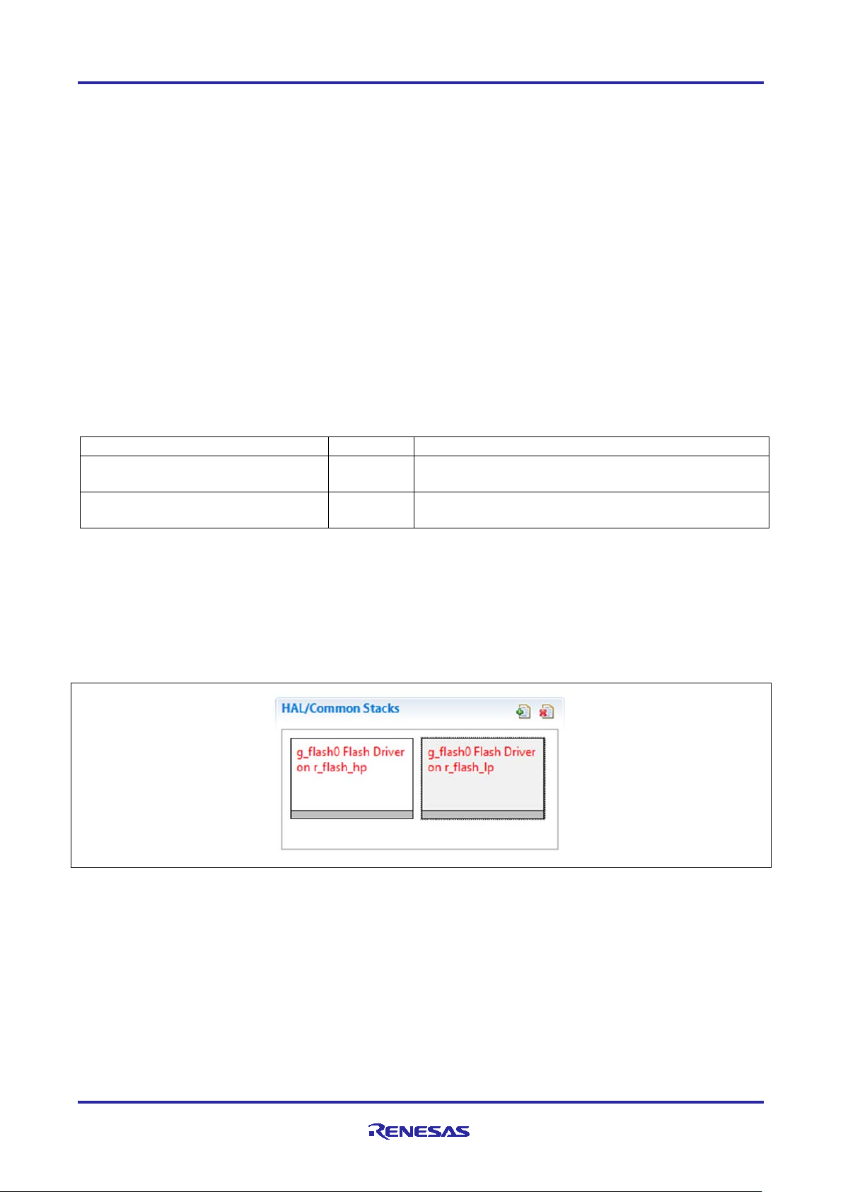
When the Flash HAL modules on r_flash_hp or r_flash_lp are added to the thread stack as shown in the
figure below, the configurator automatically adds any needed lower-level modules. Any drivers that need
additional configuration information is box text highlighted in Red. Modules with a Gray band are individual
modules that stand alone.
Note: The following figure shows both Flash HAL modules. Only one module should be used, depending on
the selected MCU; they are only shown together for completeness.
Figure 2. Flash HAL Module Stack
5. Configuring the Flash HAL Module
The Flash HAL module must be configured by the user for the desired operation. The SSP configuration
window automatically identifies (by highlighting the block in red) any required configuration selections, such
as interrupts or operating modes, which must be configured for lower-level modules for successful operation.
Only those properties that can be changed without causing conflicts are available for modification. Other
properties are ‘locked’ and are not available for changes and are identified with a lock icon for the ‘locked’
property in the Properties window in the ISDE. This approach simplifies the configuration process and
makes it much less error prone than previous ‘manual’ approaches to configuration. The available
configuration settings and defaults for all the user-accessible properties are given in the Properties tab
within the SSP configurator and are shown in the following tables for easy reference.
R11AN0087EU0120 Rev.1.20 Page 6 of 17
Apr.29.19
Page 7

Renesas Synergy™ Platform Flash HAL Module Guide
ISDE Property
Value
Description
Parameter Checking
BSP, Enabled, Disabled
(Default: BSP)
Controls whether to include code for API
parameter checking.
Code-flash Programm ing
Enable, Disabled (Default:
Controls whether or not code-flash
the amount of ROM used by the API.
Name
g_flash0
Module name.
Data-flash Background
Enabled, Disabled (Default:
Enabling allows Flash API calls that
background.
Callback
NULL
Callback function called when a data-flash
system.
Flash Ready Interrupt
Priority 0 (highest), Priority 1:2,
(Default: Disabled)
Flash ready interrupt priority selection.
Flash Error Interrupt
Priority 0 (highest), Priority 1:2,
(Default: Disabled)
Flash error interrupt priority selection.
One of the properties most often identified as requiring a change is the interrupt priority; this configuration
setting is available within the Properties window of the associated module. Simply select the indicated
module and then view the Properties window; the interrupt settings are often toward the bottom of the
properties list, so scroll down until they become available. Also note that the interrupt priorities listed in the
Properties win do w in the ISDE includ e an indication as to the validity of the setting based on the targeted
MCU (CM4 or CM0+). This level of detail is not included in the following conf ig urat ion pr op ert ies tables but is
easily visible with the ISDE when configur i ng inter r upt-priority leve ls .
Note: You may want to open your ISDE, create the module and explore the property settings in parallel with
looking over the configuration table settings in the following tables. This helps to orient you and can
be a useful ‘hands-on’ approach to learning the ins and outs of developing with SSP.
The Flash HAL Driver is implemented on one of two different modules, the r_flash_hp and the
r_flash_lp, and the configuration settings for these implementations are given in the following tables.
Table 5. Configuration Settings for the Flash HAL Module on r_flash_hp
Enable
Operation
Priority
Disabled)
Enabled)
Priority 3 (CM4: valid, CM0+:
lowest- not valid if using
ThreadX), Priority 4:14 (CM4:
valid, CM0+: invalid), Priority
15 (CM4 lowest - not valid if
using ThreadX, CM0+: invalid)
programming is enabled. Disabling reduces
reference data-flash to return immediately,
with the operation continuing in the
BGO operation completes or errors. A user
callback function can be registered in open.
Warning: Since the callback is called from
an ISR, do not use blocking calls or lengthy
processing. Spending excessive time in an
ISR can affect the responsiveness of the
Priority
Note: The example values and defaults are for a project using the Synergy S7G2. Other MCUs may have
different default values and available configuration settings.
R11AN0087EU0120 Rev.1.20 Page 7 of 17
Apr.29.19
Priority 3 (CM4: valid, CM0+:
lowest- not valid if using
ThreadX), Priority 4:14 (CM4:
valid, CM0+: invalid), Priority
15 (CM4 lowest - not valid if
using ThreadX, CM0+: invalid)
Page 8

Renesas Synergy™ Platform Flash HAL Module Guide
ISDE Property
Value
Description
Parameter Checking
BSP, Enabled, Disabled
(Default: BSP)
Controls whether to include code for API
parameter checking.
Code-flash Programming
Enable, Disabled
Controls whether or not code-flash
Name
g_flash0
Module name.
Data-flash Background
Enabled, Disabled
Enabling allows Flash API calls that
in the background.
Callback
NULL
Callback function called when a data-flash
responsiveness of the system.
Flash Ready Interrupt
Priority 0 (highest), Priority
Flash ready interrupt priority selection.
Table 6. Configuration for the Flash HAL Module on r_flash_lp
Enable
Operation
Priority
Note: The example values and defaults are for a project using the Synergy S3A7 MCU. Other MCUs may
have different default values and available configuration settings.
In some cases, settings other than the defaults can be desirable. For example, it might be useful to disable
code-flash programming to reduce the code size of the driver.
(Default: Disabled)
(Default: Enabled)
1:2, Priority 3 (CM4: valid,
CM0+: lowest- not valid if
using ThreadX), Priorit y 4:14
(CM4: valid, CM0+: invalid),
Priority 15 (CM4 lowest - not
valid if using ThreadX, CM0+:
invalid) (Default: Disabled)
programming is enabled. Disabling
reduces the amount of ROM used by the
API.
reference data-flash to return
immediately, with the operation continuing
BGO operation completes or errors. A
user callback function can be registered in
open.
Warning: Since the callback is called from
an ISR, do not use blocking calls or
lengthy processing. Spending excessive
time in an ISR can affect the
5.1 Flash HAL Module Clock Configuration
Enable the flash-ready interrupt only if you plan to use the data-flash BGO (background mode operation.) In
this mode, the application can initiate a data-flash operation and then be asynchronously notified of its
completion (or an error) using a user-supplied callback function. The callback function is passed a structure
containing event information that indicates the source of the callback event (for example,
FLASH_EVENT_ERASE_COMPLETE.)
To enable interrupts, set the priority of the FCU > FRDYI interrupt on the ICU tab of the Project Configurator
2
studio. This sets BSP_IRQ_CFG_FCU_FRDYI in synergy_cfg/ssp_cfg/bsp/bsp_irq_cfg.h to
in e
the priority level selected.
When the FLASH FRDYI interrupt is enabled in the BSP, the corresponding ISR is defined in the Flash
driver. The ISR calls a user-callback function if one was registered in open.
Note: Flash HP supports an additional flash-error interrupt and if BGO mode is enabled for FLASH HP, then
both FRDYI and FIFERR interrupts must be given a priority.
5.2 Flash HAL Module Clock Configuration
The flash circuit uses FCLK as its clock. FCLK must be <= 4 MHz. If this clock rate changes after the flash
open() function is called, then you must call updateFlashClockFreq() to inform the flash API of the
change.
R11AN0087EU0120 Rev.1.20 Page 8 of 17
Apr.29.19
Page 9

Renesas Synergy™ Platform Flash HAL Module Guide
5.3 Flash HAL Module Pin Configuration
The flash circuit does not use any MCU pins.
6. Using the Flash HAL Module in an Application
Some typical steps in using the Flash HAL module in an application are as follows:
1. Initialize the Flash HAL using the open API.
2. Disable Interrupts.
3. Blank check a code flash area with the blankCheck API.
4. Erase one or more code-flash blocks with the erase API.
5. Write to code-flash with th e write API.
6. Enable Interrupts.
7. Blank check a data flash area with the blankCheck API.
8. Erase one or more data-flash blocks using the erase API.
9. Write to data-flash using the write API.
10. Close using the close API if finished with all Flash operations.
Figure 3. Flow Diagram of a Typical Flash HP HAL Module Application
7. The Flash HAL Module Application Project
The application project associated with this module guide demonstrates the aforementioned steps in a full
design. You may want to import and open the application project within the ISDE and view the configuration
settings for the Flash HAL Module. You can also read over the code (in flash_hp_hal_mg.c/.h and
flash_hp_hal_api_mg.h), which are used to illustrate the Flash HAL module APIs in a complete design.
The application project demonstrates the typical use of the Flash HAL module APIs. The application project
HAL entry initializes the Flash HP HAL module; it also calls Flash HP application-entry function and after
Flash HP operations are executed, the application project toggles the LED periodically.
R11AN0087EU0120 Rev.1.20 Page 9 of 17
Apr.29.19
Page 10

Renesas Synergy™ Platform Flash HAL Module Guide
Resource
Revision
Description
e2 studio
v7.3.0 or later
Integrated Solution Development Environment
SSP
v1.6.0 or later
Synergy Software Platform
IAR EW for Synergy
v8.23.3 or later
IAR Embedded Workbench® for Renesas Synergy™
SSC
v7.3.0 or later
Synergy Standalone Configurator
SK-S7G2
v3.0 to v3.3
Starter Kit
The entry function to perform Flash operations is defined in flash_hp_hal_mg.c. It initializes semi-hosting
if enabled from the header file, calls an open function call to initialize the Flash HAL module, and calls
code/data-flash operations. After the flash operations are performed, the program gets back to the
hal_entry.c to execute the LED toggle.
The code-flash function block includes APIs for the code-flash to blank check a sector, erase a sector, read
data, write data, set the access window, and clear the access window. These APIs are used to demonstrate
each operation and its results, enable semi-hosting to print the results with error codes in the Console
window.
The data-flash function block includes uses of APIs for the data-flash to blank check a sector, erase a sector,
write data, and read data. These APIs are used in a particular order to demonstrate each operation and its
results. You can enable semi-hosting to print the results with error codes in the console. Also, this function
block demonstrates BGO operations and the use of callback functions for the data-flash.
All the Flash HP HAL APIs are used in the flash_hp_hal_api_mg.h header file and the
flash_hp_hal_mg.h header file contains macros for the Flash HP HAL application project.
Table 7. Software and Hardware Resources Used by the Application Project
The following figures show simple Application Project flows.
Figure 4. Flash HAL Module Application Project Flow Diagram
R11AN0087EU0120 Rev.1.20 Page 10 of 17
Apr.29.19
Page 11

Renesas Synergy™ Platform Flash HAL Module Guide
Figure 5. Flash HAL Module Application Project – Code-flash Operations – Flow Diagram
The complete application project can be found using the link provided in the References section in this
document. Locate flash_hp_hal_mg.c/.h and flash_hp_hal_api_mg.h in the project once it has
been imported into the ISDE. You can open this file within the ISDE and follow along with the description
provided to help identify key uses of APIs.
As mentioned above, the flash_hp_hal_mg.c contains APIs to initialize Flash HP HAL and functions to
execute data/code-flash operations. The code-flash function block demonstrates various code-flash
operations. The code-flash operations function block uses the read, write, erase, blank check and set/clear
flash access window operations. There is no particular flow of operations for the Flash HP. The APIs can be
used standalone as per the application’s requirements.
R11AN0087EU0120 Rev.1.20 Page 11 of 17
Apr.29.19
Page 12

Renesas Synergy™ Platform Flash HAL Module Guide
Figure 6. Flash HAL Module Application Pr oject - Data-flash Operations - Flow Diagram
The data-flash function block demonstrates various data-flash operations. The data-flash operations function
block uses read, write, erase and blank check data-flash operations. There is no particular flow of operations
for Flash HP for data-flash; the APIs can be used as standalone as per the application’s requirements. Both
data and code-flash opera ti ons use the same APIs with respective flash addresses as parameters.
The last section is the user-callback function. Data-flash background operations (BGO) can be non-blocking,
that is, the function call returns immediately after it is called and an interrupt is gener ate d when the oper a tio n
is completed. The callback function handles interrupts for the Flash HP and sets flags to be used in Flash
operations.
The flash_hp_hal_mg.h file contains macro for memory addresses that are used in Flash APIs, write
bytes, semi-hosting enable/disable and function prototypes.
Note: This description assumes that you are familiar with using printf() for the Debug Console with the
Synergy Software Package. If you are unfamiliar with this, refer to How do I Use Printf() with the
Debug Console in the Synergy Software Package given in the References section in this document.
Alternatively, the user can see results using the watch variables in the debug mode.
A few key properties are configured in this application project to support the required operations and the
physical properties of the target board and MCU. The properties with the values set for this specific project
are listed in the following table. You can also open the application project and view these settings in the
Properties window as a hands-on exercise.
R11AN0087EU0120 Rev.1.20 Page 12 of 17
Apr.29.19
Page 13

Renesas Synergy™ Platform Flash HAL Module Guide
Resource
ISDE Property
Setting
g_flash0 Flash Driver on r_flash_hp
Parameter Checking
Disabled
Code-flash Programming Enable
Enable
FCU FRDYI
Priority3
FCU FIFERR
Priority3
Name
g_flash0
Data-flash Background Operation
Enabled
Callback
BGO_Callback
Table 8. Flash HAL Module Configuration Settings for the Application Project
8. Customizing the Flash HAL Module for a Target Application
Some user configuration settings are normally changed by the developer from those shown in the application
project. For example, you can easily change the configuration settings for code-flash programming and dataflash background operations. If code-flash programming is not required in the user application, the user can
disable code-flash programming. This also helps to make the code size smaller. The user can change the
BGO and interrupt settings from the configuration properties for data-flash operations to select between
blocking (non-BGO) or non-blocking (BGO) operations.
The application project writes to specific memory sectors of the code and data-flash. You can change API
parameters to be the memory address of the sectors they want to work with.
9. Running the Flash HAL Module Application Project
To run the Flash HAL module application project and see it executed on a target kit, you can simply import it
into your ISDE, compile and run debug. See Renesas Synergy™ Project Import Guide (r11an0023eu0121synergy-ssp-import-guide.pdf, included in this package) for instructions on importing the project into e
or IAR EW for Synergy and building/running the application.
To implement the Flash HAL module application in a new project, follow the steps below for defining,
configuring, auto-generating files, adding code, compiling and debugging on the target kit. The hands-on
approach of following these steps can help make the development process with SSP more practical, while
just reading over this guide tends to be more theoretical.
Note: The following steps are described in sufficient detail for someone experienced with the basic flow
through the Synergy development process. If these steps are not familiar, refer to the first few
chapters of the SSP User’s Manual for a description of how to accomplish these steps.
To create and run the Flash HAL module application project, simply follow these steps:
2
1. Import attached Example Project into e
studio or IAR EW for Synergy. For steps to import an example
project, see Renesas Synergy™ Project Import Guide (r11an0023eu0121-synergy-ssp-import-guide.pdf,
included in this package).
2. Compile the application without errors or warnings.
3. Connect to the host PC via a micro USB cable to J19 on SK-S7G2.
4. Start to debug the application.
5. The output can be viewed (see figure), if semi-hosting is enabled from the flash_hp_hal_mg.h file.
Note: LED1-3 toggles after flash operations are executed. By default, the application project executes data-
flash operations. To execute code-flash operations, change the 1 to a 0 on line 533 in the
flash_hp_hal_mg.c file.
2
studio
R11AN0087EU0120 Rev.1.20 Page 13 of 17
Apr.29.19
Page 14

Renesas Synergy™ Platform Flash HAL Module Guide
Figure 7. Example Output from Flash HAL Module Applicatio n Project – Data-flash Operations BGO
(Non-Blocking), Default Operation
Figure 8. Example Output from Flash HAL Module Application Project – Code-flash Operations
R11AN0087EU0120 Rev.1.20 Page 14 of 17
Apr.29.19
Page 15

Renesas Synergy™ Platform Flash HAL Module Guide
Figure 9. Example Output from Flash HAL Module Applicatio n Project – Data-flash Operations Non-
BGO (Blocking)
10. Flash HAL Module Conclusion
This module guide has provided all the background information needed to select, add, configure, and use the
Flash HP/LP module in an example project. Many of these steps were time consuming and error-prone
activities in previous generations of embedded systems. The Renesas Synergy™ Platform makes these
steps much less time consuming and removes the common errors, like conflicting configuration settings or
the incorrect selection of lower-level drivers. The use of high-level APIs (as demonstrated in the application
project) illustrate additional development time savings by allowing work to begin at a high level and avoiding
the time required in older development environments to use or, in some cases, create, lower-level drivers.
11. Flash HAL Module Next Steps
After you have mastered a simple Flash HP HAL Module application projec t, you may want to use the APIs
that manipulates flash from the application during run time. (For example, a secondary bootloader.) These
APIs can also be used to write and read the program status to flash memory at run time.
12. Flash HAL Module Reference Information
SSP User Manual: Available in html format in the SSP distribution package and as a pdf from the Synergy
Gallery.
Links to all the most up-to-date r_flash module reference materials and resources are available on the
Synergy Knowledge Base:
us.knowledgebase.renesas.com/English_Content/Renesas_Synergy%E2%84%A2_Platform/Renesas_Syne
rgy_Knowledge_Base/r__flash_Module_Guide_Resources.
https://en-
R11AN0087EU0120 Rev.1.20 Page 15 of 17
Apr.29.19
Page 16

Renesas Synergy™ Platform Flash HAL Module Guide
Website and Support
Visit the following vanity URLs to learn about key elements of the Synergy Platform, download components
and related documentation, and get support.
Synergy Software www.renesas.com/synergy/software
Synergy Software Package www.renesas.com/synergy/ssp
Software add-ons www.renesas.com/synergy/addons
Software glossary www.renesas.com/synergy/softwareglossary
Development tools www.renesas.com/synergy/tools
Synergy Hardware www.renesas.com/synergy/hardware
Microcontrollers www.renesas.com/synergy/mcus
MCU glossary www.renesas.com/synergy/mcuglossary
Parametric search www.renesas.com/synergy/parametric
Kits www.renesas.com/synergy/kits
Synergy Solutions Gallery www.renesas.com/synergy/solutionsgallery
Partner projects www.renesas.com/synergy/partnerprojects
Application projects www.renesas.com/synergy/applicationprojects
Self-service support resources:
Documentation www.renesas.com/synergy/docs
Knowledgebase www.renesas.com/synergy/knowledgebase
Forums www.renesas.com/synergy/forum
Training www.renesas.com/synergy/training
Videos www.renesas.com/synergy/videos
Chat and web ticket www.renesas.com/synergy/resourcelibrary
R11AN0087EU0120 Rev.1.20 Page 16 of 17
Apr.29.19
Page 17

Renesas Synergy™ Platform Flash HAL Module Guide
Rev.
Date
Description
Page
Summary
1.00
May.15.17
-
Initial Release
1.01
Aug.1.17
11
Update to Hardware and Software Resources Table
1.10
Nov.13.18
-
Changed Note before Fig 7 and changed Fig 7/8/9 order
1.20
Apr.29.19
-
Added new API information. Updated for SSP v1.6.0.
13. Revision History
R11AN0087EU0120 Rev.1.20 Page 17 of 17
Apr.29.19
Page 18

Corporate Headquarters
Contact information
www.renesas.com
Trademarks
of their respective owners.
Notice
1. Descriptions of circuits, software and other related information in this document are provided only to illustrate the operation of semiconductor products
and application examples. You are fully responsible for the incorporation or any other use of the circuits, software, and information in the design of your
product or system. Renesas Electronics disclaims any and all liability for any losses and damages incurred by you or third parties arising from the use
of these circuits, software, or information.
2. Renesas Electronics hereby expressly disclaims any warranties against and liability for infringement or any other claims involving patents, copyrights,
or other intellectual property rights of third parties, by or arising from the use of Renesas Electronics products or technical information described in this
document, including but not limited to, the product data, drawings, charts, programs, algorithms, and application examples.
3. No license, express, implied or otherwise, is granted hereby under any patents, copyrights or other intellectual property rights of Renesas Electronics
or others.
4. You shall not alter, modify, copy, or reverse engineer any Renesas Electronics product, whether in whole or in part. Renesas Electronics disclaims any
and all liability for any losses or damages incurred by you or third parties arising from such alteration, modification, copying or reverse engineering.
5. Renesas Electronics products are classified according to the following two quality grades: “Standard” and “High Quality”. The intended applications for
each Renesas Electronics product depends on the product’s quality grade, as indicated below.
"Standard": Computers; office equipment; communications equipment; test and measurement equipment; audio and visual equipment; home
"High Quality": Transportation equipment (automobiles, trains, ships, etc.); traffic control (traffic lights); large-scale communication equipment; key
Unless expressly designated as a high reliability product or a product for harsh environments in a Renesas Electronics data sheet or other Renesas
Electronics document, Renesas Electronics products are not intended or authorized for use in products or systems that may pose a direct threat to
human life or bodily injury (artificial life support devices or systems; surgical implantations; etc.), or may cause serious propert y dama ge (space
system; undersea repeaters; nuclear power control systems; aircraft control systems; key plant systems; military equipment; etc.). Renesas Electronics
disclaims any and all liability for any damages or losses incurred by you or any third parties arising from the use of any Renesas Electronics product
that is inconsistent with any Renesas Electronics data sheet, user’s manual or other Renesas Electronics document.
6. When using Renesas Electronics products, refer to the latest product information (data sheets, user’s manuals, application notes, “General Notes for
Handling and Using Semiconductor Devices” in the reliability handbook, etc.), and ensure that usage conditions are within the ranges specified by
Renesas Electronics with respect to maximum ratings, operating power supply voltage range, heat dissipation characteristics, installation, etc. Renesas
Electronics disclaims any and all liability for any malfunctions, failure or accident arising out of the use of Renesas Electronics produ cts outside of such
specified ranges.
7. Although Renesas Electronics endeavors to improve the quality and reliability of Renesas Electronics products, semiconductor products have specific
characteristics, such as the occurrence of failure at a certain rate and malfunctions under certain use conditions. Unless designated as a high reliability
product or a product for harsh environments in a Renesas Electronics data sheet or other Renesas Electronics document, Renesas Electronics
products are not subject to radiation resistance design. You are responsible for implementing safety measures to guard against the possibility of bodily
injury, injury or damage caused by fire, and/or danger to the public in the event of a failure or malfunction of Renesas Electronics products, such as
safety design for hardware and software, including but not limited to redundancy, fire control and malfunction prevention, appropriate treatment for
aging degradation or any other appropriate measures. Because the evaluation of microcomputer software alone is very difficult and im pr acti c al, you are
responsible for evaluating the safety of the final products or systems manufactured by you.
8. Please contact a Renesas Electronics sales office for details as to environmental matters such as the environmental compatibility of each Renesas
Electronics product. You are responsible for carefully and sufficiently investigating applicable laws and regulations that regulate the inclusion or use of
controlled substances, including without limitation, the EU RoHS Directive, and using Renesas Electronics products in compliance with al l these
applicable laws and regulations. Renesas Electronics disclaims any and all liability for damages or losses occurring as a result of your noncompliance
with applicable laws and regulations.
9. Renesas Electronics products and technologies shall not be used for or incorporated into any products or systems whose manufacture, use, or sale is
prohibited under any applicable domestic or foreign laws or regulations. You shall comply with any applicable export control laws and regulations
promulgated and administered by the governments of any countries asserting jurisdiction over the parties or transactions.
10. It is the responsibility of the buyer or distributor of Renesas Electronics products, or any other party who distributes, disposes of, or otherwise sells or
transfers the product to a third party, to notify such third party in advance of the contents and conditions set forth in this document.
11. This document shall not be reprinted, reproduced or duplicated in any form, in whole or in part, without prior written consent of Renesas Electronics.
12. Please contact a Renesas Electronics sales office if you have any questions regarding the information contained in this document or Renesas
Electronics products.
(Note1) “Renesas Electronics” as used in this document means Renesas Electronics Corporation and also includes its directly or indirectly controlled
(Note2) “Renesas Electronics product(s)” means any product developed or manufactured by or for Renesas Electronics.
subsidiaries.
electronic appliances; machine tools; personal electronic equipment; industrial robots; etc.
financial terminal systems; safety control equipment; etc.
(Rev.4.0-1 Novembe r 201 7)
TOYOSU FORESIA, 3-2-24 Toyosu,
Koto-ku, Tokyo 135-0061, Japan
Renesas and the Renesas logo are trademarks of Renesas Electronics
Corporation. All trademarks and registered trademarks are the property
For further information on a product, technology, the most up-to-date
version of a document, or your ne are s t sales office, please visit:
www.renesas.com/contact/
.
© 2019 Renesas Electronics Corporation. All rights reserved.
 Loading...