

Page 1
User's Manual
R12UZ0065EJ0110 Rev.1.10 Page 1 of 54
2020.11.06
Evaluation System for Stepping Motor with Resolver
User's Manual
Safety Precautions
Be sure to read this manual before using the Evaluation System for Stepping Motor with Resolver
(RTK0EMX270S01020BJ) (Called "this product" below).
・ Follow the instructions in this manual when using this product.
・ Keep this manual near this product so you can refer to it whenever necessary.
・ Transfer or sale of this product to third parties is prohibited without written approval.
・ The purchaser or importer of this product shall ensure compliance with local regulations. In addition, the
customer is responsible for ensuring that this product is handled correctly and safely, in accordance with the laws
of the customer's country (region).
・ The manuals and specifications related to this product (called "the documents, etc." below) are tools that were
developed for the function and performance evaluation of Renesas Electronics semiconductor devices (called
"Renesas Electronics devices" below) mounted on this product and do not guarantee the quality, function, and
performance equivalent to Renesas Electronics products.
・ By purchasing this product or downloading the documents, etc. from Renesas Electronics website, the support
services provided from Renesas Electronics are not guaranteed.
・ All information contained in this manual represents information on products at the time of publication of this
manual. Note that the product data, specifications, contact for inquiries, contents of website, address, etc., are
subject to change by Renesas Electronics Corporation without notice. Confirm the latest information on Renesas
Electronics website, etc.
In this manual, items related to the safe use of the product are indicated as described below.
■The degree of injury to persons or damage to property that could result if the designated instruction in this manual
is not followed is indicated as follows.
Danger
Indicates a thing that, if not followed, could result in
death or serious injury(*1) to the user, and which is
highly imminent.
Warning
Indicates a thing that, if not followed, could result in
death or serious injury to the user.
Caution
Indicates a thing that, if not followed, could result in
injury(*2) to persons or physical damage(*3).
*1 Serious injury refers to conditions resulting in persistent after-effects and for which treatment would
necessitate hospitalization or regular hospital visits, such as loss of eyesight, burns (high- or low-
temperature), electric shock, bone fracture, poisoning, or other injuries.
*2 Injury refers to conditions for which treatment would necessitate hospitalization or regular hospital visits.
*3 Physical damage refers to damage affecting the wider surroundings, such as the user's home or property.
Meaning of Notations
R12UZ0065EJ0110
Rev.1.10
2020.11.06
Page 2
Evaluation System for Stepping Motor with Resolver User's Manual
R12UZ0065EJ0110 Rev.1.10 Page 2 of 54
2020.11.06
■Requirements related to the handling of the product are classified into the following categories.
・Marks indicating that an action is prohibited
General prohibition
The indicated action is prohibited.
(Example) Do not touch.
Touching the specified location could
result in injury.
・Marks indicating that an action requires caution.
General caution
Indicates a general need for caution
that is not specified.
(Example) High temperature
Indicates the possibility of injury due to
high temperature.
・Marks directing that the specified action is required
General instruction
The specified action is required.
(Example) Turn off (disconnect) power.
Instructs the user to turn off (disconnect)
the power to the product.
Danger
・The product should be used only by persons having a thorough knowledge of electrical and mechanical
components and systems, a full knowledge of the risks associated with handling them, and training in
inverter motor control and handling motors, or equivalent skills (called "users" below). Users should be
limited to persons who have carefully read the Caution Items contained in this manual.
・Unlike typical equipment, this product has no protective case to ensure safety, and it contains moving
parts and high-temperature components that could be dangerous. Do not touch the evaluation board or
cables while power is being supplied.
・Carefully check to make sure that there are no pieces of conductive materials or dust adhering to the
board, connectors, and cables.
・There are moving parts, driven by a motor. Do not touch the motor while power is being supplied.
・Ensure that the motor is insulated and placed in a stable location before supplying power.
Do not connect load to motor.
・This could cause fire, burns, or injury.
Warnings Regarding Use of the Product
■Danger Items
Page 3
Evaluation System for Stepping Motor with Resolver User's Manual
R12UZ0065EJ0110 Rev.1.10 Page 3 of 54
2020.11.06
Warning
Caution - Rotating parts
・The system includes a motor. Touching the rotating shaft could cause high-temperature burns or injury.
Insert plugs, connectors, and cables securely, and confirm that they are fully inserted.
・Incomplete connections could cause fire, burns, electric shock, or failures.
Use the power supply apparatus specified in the manual.
・Failure to do so could cause fire, burns, electric shock, injury, or failures.
Stop supplying power and unplug all cables when the product will not be used for a period of time or when
moving the product.
・Failure to do so could cause heat, fire, burns, electric shock, or failures.
・This will protect the product against damage due to lightning.
Use a mechanism (switch, outlet, etc.) located within reach to turn off (disconnect) the power supply.
・If an abnormality occurs, it may be necessary to cut off the power supply quickly.
Stop supplying power immediately if you notice abnormal odor, smoke, abnormal sound, or overheating.
・Continuing to use the product in an abnormal condition could cause fire, burns, or electric shock.
Do not disassemble, modify, or repair the product.
・Doing so could cause fire, burns, electric shock, injury, or failures.
Do not use this product for any purpose other than initial evaluation of motor control in a testing room or
laboratory.
Do not integrate the product or any part of it into other equipment.
Do not insert or remove cables or connectors when the product is powered on.
・The product has no safety case.
・Failure to observe the above could cause fire, electric shock, burns, or failures.
・The product may not perform as expected if used for other than its intended purpose.
Caution
High temperature
・The motor gets hot. Touching it could cause high-temperature burns.
Follow the procedure specified in the manual when turning the power to each system on or off.
・Failure to do so could cause overheating or failures in devices.
Attention to static charge
Before using this product, wear an antistatic wrist strap. If you touch this product with a static
charge on your body, a device failure may occur or operation may become unstable.
Before using this product, mount the ferrite core near this product on each cable for connecting
this product and stabilized power supply.
・Failure to do so could interfere with operation of other devices or cause failures in the devices.
■Warning Items
■Caution Items
Page 4

Evaluation System for Stepping Motor with Resolver User's Manual
R12UZ0065EJ0110 Rev.1.10 Page 4 of 54
2020.11.06
Information Related to Regulations
European Union regulatory notices
This product complies with the following EU Directives. (These directives are only valid in the European Union.)
CE Certifications:
・Electromagnetic Compatibility (EMC) Directive 2014/30/EU
EN61326-1 : 2013 Class A
WARNING: This is a Class A product. This equipment can cause radio frequency noise when used in the
residential area. In such cases, the user/operator of the equipment may be required to take
appropriate countermeasures under his responsibility.
・Information for traceability
・Authorised representative
Name: Renesas Electronics Corporation
Address: Toyosu Foresia, 3-2-24, Toyosu, Koto-ku, Tokyo 135-0061, Japan
・Manufacturer
Name: Renesas Electronics Corporation
Address: Toyosu Foresia, 3-2-24, Toyosu, Koto-ku, Tokyo 135-0061, Japan
・Person responsible for placing on the market
Name: Renesas Electronics Europe GmbH
Address: Arcadiastrasse 10, 40472 Dusseldorf, Germany
・Trademark and Type name
Trademark: Renesas
Product name: Evaluation System for Stepping Motor with Resolver
Type name: RTK0EMX270S01020BJ
Environmental Compliance and Certifications:
・Waste Electrical and Electronic Equipment (WEEE) Directive 2012/19/EU
Page 5

Evaluation System for Stepping Motor with Resolver User's Manual
R12UZ0065EJ0110 Rev.1.10 Page 5 of 54
2020.11.06
Overview of This Product
The Evaluation System for Stepping Motor with Resolver is a motor control evaluation kit.
This product has a resolver/digital converter IC manufactured by Renesas Electronics, which enables high resolution
position control in combination with the motor with a resolver supplied with this product.
The product is equipped with various external device interfaces, which enables you to start the evaluation of the
stepping motor with a resolver immediately by connecting a general motor control device.
In addition, this product supports the support tool for motor control development manufactured by Renesas
Electronics (Renesas Motor Workbench). Renesas Motor Workbench can display internal variables of a microcontroller
in waveform in real time and automatically extract vector control parameters, which enables efficient software
development.
This user's manual describes how to handle this product. On this product, the connectors other than those required for
quick start are not basically mounted at the factory. To use an interface described in this user's manual, it may be
necessary to mount a required connector.
Mounted devices
Microcontroller: R5F524TEADFP
Resolver/digital converter: RAA3064002GFP
Gate driver: HIP4082IBZ
RS-485 driver: ISL3156EIUZ
CAN driver: R2A25416SP
MOSFET: RJK1054DPB
Regulator: ISL9001AIRNZ, ISL9005AIRNZ
Related documents
⚫ Related to 48V 2A inverter board for stepping motor
➢ Circuit diagram: R12TU0083
➢ Parts list: R12TU0085
➢ PCB pattern diagram: R12TU0087
⚫ Related to RX24T CPU card with RDC-IC
➢ Circuit diagram: R12TU0082
➢ Parts list: R12TU0084
➢ PCB pattern diagram: R12TU0086
⚫ Related to the support tool for motor control development "Renesas Motor Workbench"
➢ User's Manual: R21UZ0004
⚫ Sample code
➢ Application note: R03AN0014
Included items
Refer to the "Included Items" supplied with this product.
Page 6
Evaluation System for Stepping Motor with Resolver User's Manual
R12UZ0065EJ0110 Rev.1.10 Page 6 of 54
2020.11.06
Abbreviations
Abbreviation
Formal name
Remarks
this product
Evaluation System for Stepping Motor with
Resolver
Model name: RTK0EMX270S01020BJ
inverter board
48V 2A inverter board for stepping motor
Model name: RTK0EM0000B11020BJ
CPU card
RX24T CPU card with RDC-IC
Model name: RTK0EMX270C02000BJ
RMW
Support tool for motor control development
"Renesas Motor Workbench"
Support tool for motor control
development manufactured by Renesas
Electronics
MCU
microcontroller
Microcontroller mounted on this product
(Model name: R5F524TEADFP)
RDC IC
resolver/digital converter IC
Resolver/digital converter IC mounted
on this product
(Model name: RAA3064002GFP)
Page 7

Evaluation System for Stepping Motor with Resolver User's Manual
R12UZ0065EJ0110 Rev.1.10 Page 7 of 54
2020.11.06
Contents
Safety Precautions .................................................................................................................... 1
Information Related to Regulations ........................................................................................... 4
Overview of This Product .......................................................................................................... 5
Overview of the Product ..................................................................................................... 8
1.1 Specifications ................................................................................................................................ 8
1.2 Block Diagram ............................................................................................................................... 9
1.3 Layout .......................................................................................................................................... 10
Using This Product ........................................................................................................... 11
2.1 Quick Start 1 Connection and Board Operations ..................................................................... 11
2.2 Quick Start 2 GUI Operations ................................................................................................... 15
2.3 Initial Software Specifications ..................................................................................................... 23
2.4 Writing to Flash Memory ............................................................................................................. 24
2.5 Troubleshooting .......................................................................................................................... 25
Kit Specifications .............................................................................................................. 27
3.1 Specification List ......................................................................................................................... 27
3.2 Stepping Motor with Resolver ..................................................................................................... 28
3.3 Power Supply .............................................................................................................................. 29
3.4 Inverter Circuit ............................................................................................................................. 30
3.5 Sensor Interfaces ........................................................................................................................ 34
3.6 External Device Interfaces .......................................................................................................... 37
3.7 User Interfaces ............................................................................................................................ 44
3.8 Pin Assignments ......................................................................................................................... 46
How to Flash Program MCU ............................................................................................ 51
Website and Support ............................................................................................................... 54
Revision History ....................................................................................................................... 55
General Precautions in the Handling of Microprocessing Unit and Microcontroller Unit
Products ........................................................................................................................... 56
Notice ...................................................................................................................................... 57
Page 8
Evaluation System for Stepping Motor with Resolver User's Manual
R12UZ0065EJ0110 Rev.1.10 Page 8 of 54
2020.11.06
Overview of the Product
1.1 Specifications
Table 1-1 Overview of Specifications
Item
Specification
Kit name
Evaluation System for Stepping Motor with Resolver
Kit model name
RTK0EMX270S01020BJ
Kit configuration
48V 2A inverter board for stepping
motor
RTK0EM0000B11020BJ
RX24T CPU card with RDC-IC
RTK0EMX270C02000BJ
Stepping motor with resolver
R17PMK440CNVA4438
(manufactured by MinebeaMitsumi Inc.)
Rated current: 2 Apeak/Phase
With a resolver
Inverter
specifications
• Applicable motor: Stepping motor
• Rated voltage: 48 V
• Rated output: 100 W
• Detection function: Phase current, bus voltage
• Protection function: Overcurrent protection
Interface
specifications
• Applicable sensors: Resolver, encoder(*1)
• External device interfaces: RS-485(
*1
), CAN(*1), pulse train command(*1),
general-purpose in/out(
*1
)
Development
support functions
• Compatible with support tool for motor control development, Renesas Motor
Workbench
• With an on-board emulator circuit (flash programming circuit)
External view
Note: The actual product may differ from this photo.
Operating
temperature
Room temperature
Operating humidity
No condensation allowed.
Compliance: EMC
directive
Europe: EN61326-1: 2013 Class A
*1 The connector is not mounted.
Page 9
Evaluation System for Stepping Motor with Resolver User's Manual
R12UZ0065EJ0110 Rev.1.10 Page 9 of 54
2020.11.06
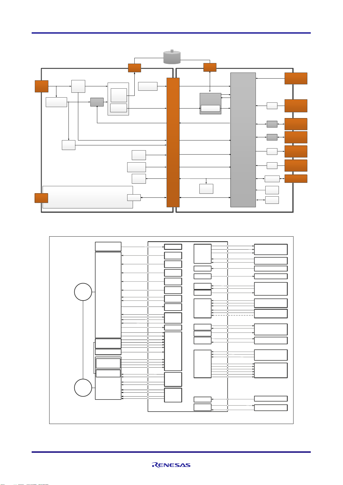
1.2 Block Diagram
Power
connector
Variable
resistor
Toggle switch/
push switch
12-V voltage
generation function
Overcurrent
detection
function
5-V voltage
generation
function
Inverter circuit
Gate Driver
Motor
connector
Board-to-
board
connector
24-48V
12V
Overcurrent detection
4-phase
compensation PWM
5V
MCU
RX24T
Origin sensor/limit
sensor interface (not
installed)
USB connector (not
installed)
Crystal
oscillator
Reset switch
LED * 3
RDC IC
Output voltage
divider
Resolver
connector
E2 On Board
RS485
CAN
Buffer
Communication circuit for motor development support tool, Renesas Motor Workbench
USB
connector
Digital
Isolator
Current detection
amplifier
LED * 2
Inverter board
Encoder/pulse train
command connector
(not installed)
CAN communication
connector (not
installed)
RS-485
communication
connector (not
installed)
General-purpose
output connector (not
installed)
General-purpose
input analog
command connector
(not installed)
Buffer
Buffer
CPU card
Shunt resistor
MOSFETs
Resolver motor
Figure 1-1 Block Diagram
Current
detection
MTU0
RDC
TMR4
MTU3
MTU4
UART6
MTU
RSCAN
A/D
ICU
Origin sensor
Limit sensor
MTU2
POE
I/O
Inverter
Upper device
RS485
Upper device
CAN
Upper device
Sequence input
Upper device
Sequence output
I/O
Supply voltage
Phase
voltage
Overcurrent
detection
Variable resistor
Switch
Analog command
Analog monitor
D/A
Resolver
Motor
LED
UART1
RMW
PE5/IRQ0
P00/IRQ2
P24/DA0
I/O
LED3
LED2
LED1
SW1
SW2
DOG
N-OT, P-OT
P33/MTCLKA
P32/MTCLKB
PA5/MTIOC1A
SPON
PD1
PA3/MTIOC2 A
PB2/TXD6
PB1/RXD6
I/O
P02
RS485_TX
RS485_RX
RS485_DE
PA0/CTXD0
PA1/CRXD0
CAN_TX
CAN_RX
P10
SVON
P65
PB7
GPINPUT
GPINPUT
PB6
PB5
PB4
PB3
PD4
PD2
COIN
ORG
GPOUTPUT
RDY
ERROR
GPOUTPUT
ICS_RX
ICS_TX
PD5/RXD1
PD3/TXD1
I/O
P64/AN204
P92/MTIOC6 D
P55/AN211
AIN
VR1
VDC
P54/AN210
VA-
VB-
VB+
VA+
P53/AN209
P52/AN208
P51/AN207
P75/MTIOC4C
P74/MTIOC3D
P72/MTIOC4A
P72/MTIOC3B
B+L
A+L
B+H
A+H
P70/POE0#
PA2
P81
P80
P61
P62
Analog_Mon
P43
P11/TMO3
PB0/TMO0
P82/TMO4
P31/MTIOC0A
TMR0
TMR3
MTU9
P21/MTIOC9A
PE0/MTIOC9B
P95/MTIOC6B
RSPI
P23/MOSI A
PA4/RSPCKA
PD6/SSLA0
P22/MISOA
HISEDE_OC
RDC_RESET
RDC_CLK
RDC_PWMINA
RDC_PWMINB
RDC_CC
RDC_CARR IER1
RDC_CARR IER2
RDC_COUT
SPI_MOSI
SPI_MISO
SPI_SCLK
SPI_SCS
P50/AN206
P47/AN103
MNTOUT_DC
MNTOUT_AC
RDC_ALARM
P01/POE12#
POE
Shunt resistor
A/D
P60/AN200
A/D
A-H
A-L
B-L
B-H
P91/MTIOC7 C
MTU6
MTU7
P94/MTIOC7 A
P44/AN100
P45/AN101
P46/AN102
P40/AN000
IA-
IA+
IB+
IB-
Encoder
Upper device
Pulse command
ENC_A
ENC_B
ENC_Z
PULSE/UP
DIR/DOWN
CLR
PE4/MTCLK C
PE3/MTCLK D
PA3/MTIOC2 A
Figure 1-2 Connection Destinations of RX24T Pins by Function
Page 10
Evaluation System for Stepping Motor with Resolver User's Manual
R12UZ0065EJ0110 Rev.1.10 Page 10 of 54
2020.11.06
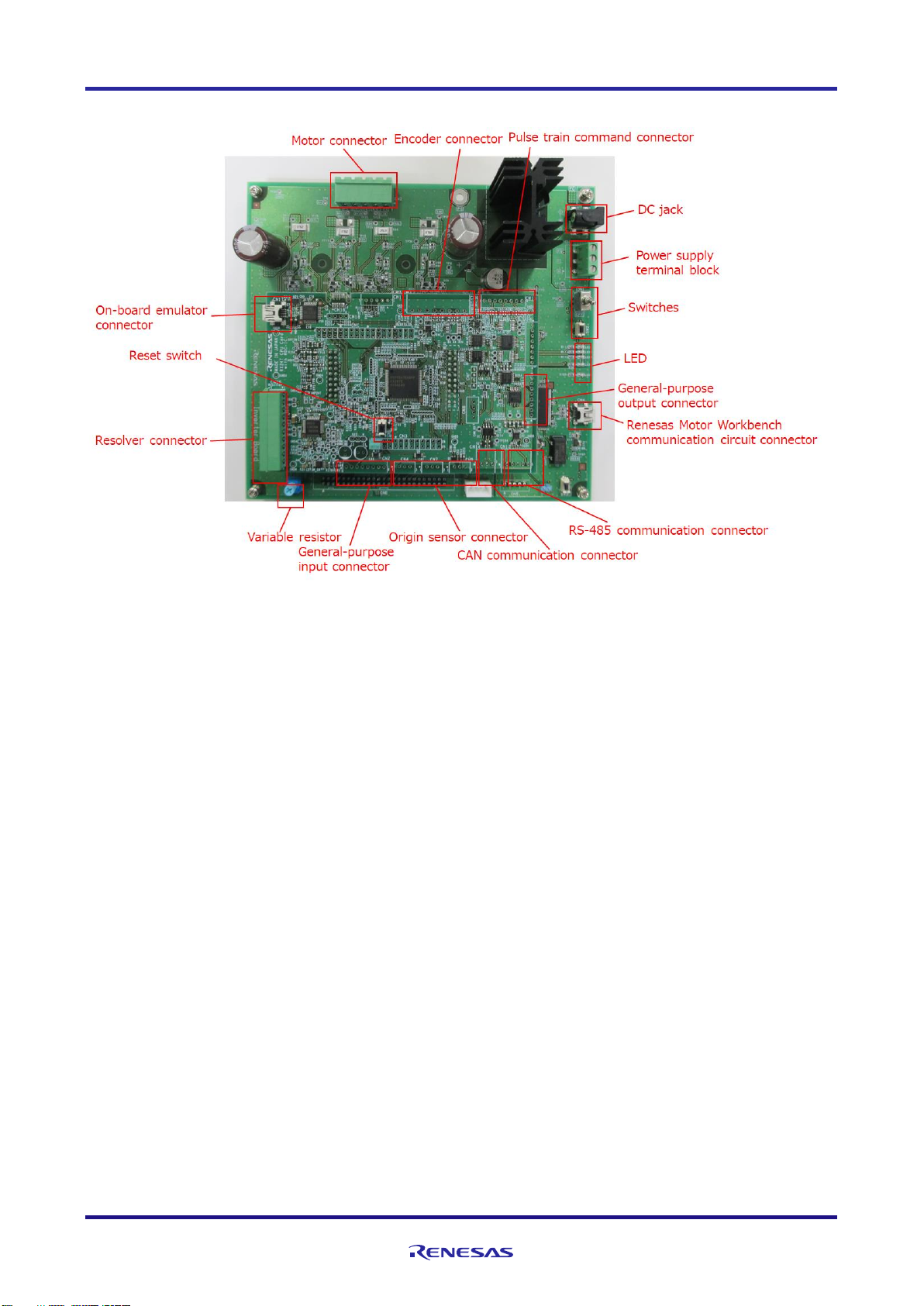
1.3 Layout
Figure 1-3 Layout
* All connectors other than the resolver connector and on-board emulator connector are not mounted on the CPU card.
* The actual product may differ from this photo.
Page 11

Evaluation System for Stepping Motor with Resolver User's Manual
R12UZ0065EJ0110 Rev.1.10 Page 11 of 54
2020.11.06
Using This Product
2.1 Quick Start 1 Connection and Board Operations
This section describes a quick start procedure of this product. Perform steps (1) to (9) in this order.
A stepping motor with resolver (called a motor below) manufactured by MinebeaMitsumi Inc. is supplied with this
product. Use the supplied motor in the procedure described in this section.
Before using this product, wear an antistatic wrist strap. If you touch this product with a static charge on your body, a
device failure may occur or operation may become unstable.
Procedure of quick start 1
Step
Operation
(1)
Connecting the motor and board
(2)
Checking the variable resistor
(3)
Connecting the stabilized power supply and board
(4)
Supplying the power
(5)
Executing the calibration
(6)
Enabling the rotation of the motor
(7)
Checking that the motor speed changes
(8)
Stopping the rotation of the motor
(9)
Stopping supplying the power
Preparation
Prepare the following items.
・Stabilized power supply: 24 VDC or higher output voltage, 1 A or higher output current
・Two power cables: Cables through which 1 A or higher current can flow (for connecting the stabilized
power supply and inverter board)
Page 12
Evaluation System for Stepping Motor with Resolver User's Manual
R12UZ0065EJ0110 Rev.1.10 Page 12 of 54
2020.11.06
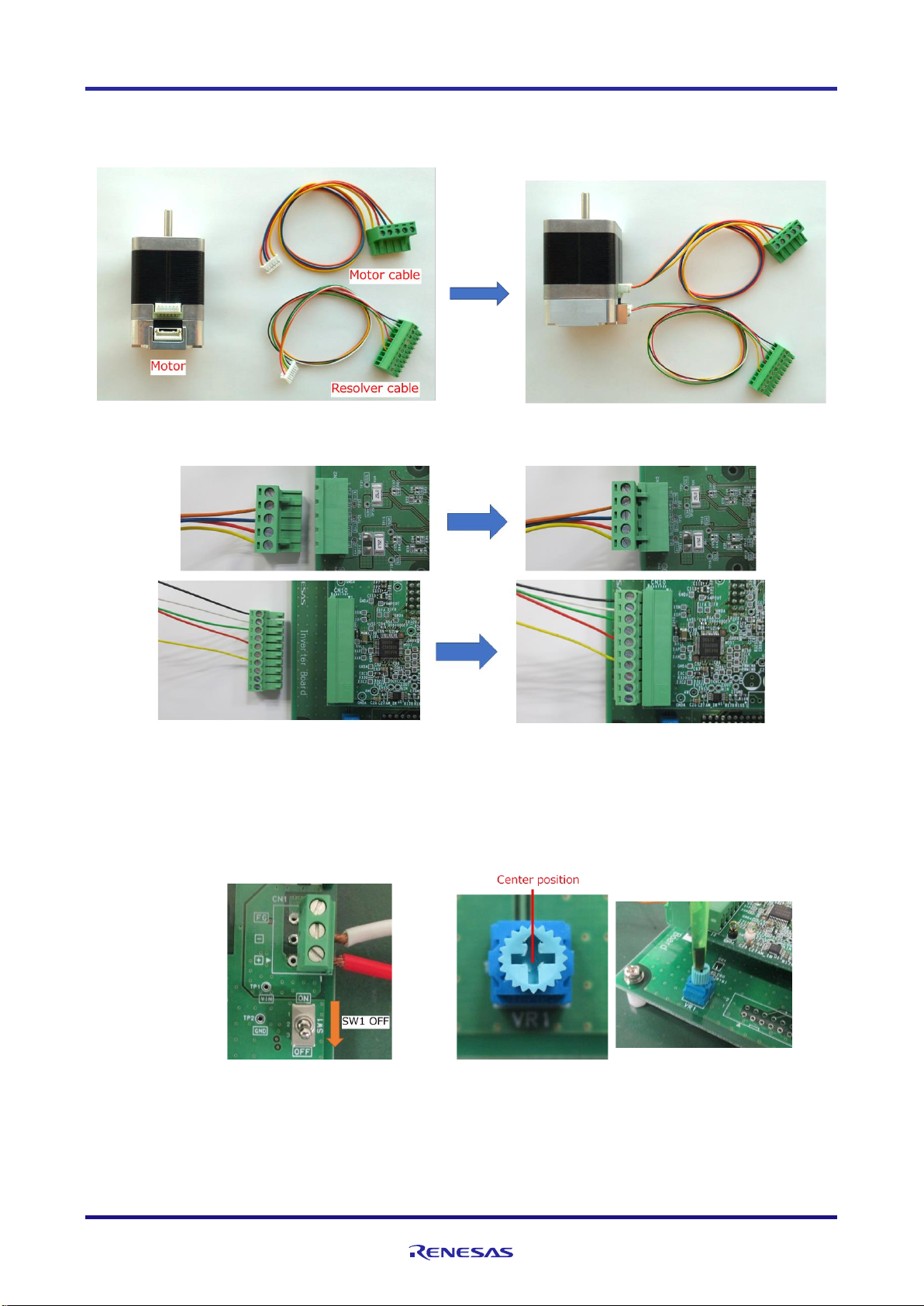
(1) Connecting the motor and board
First, connect the motor cable and the resolver cable to the supplied motor as shown in Figure 2-1. Then, connect the
motor cable to the inverter board and the resolver cable to the CPU card as shown in Figure 2-2.
Figure 2-1 Connecting the Cables to the Motor
Figure 2-2 Connecting the Cables to the Boards
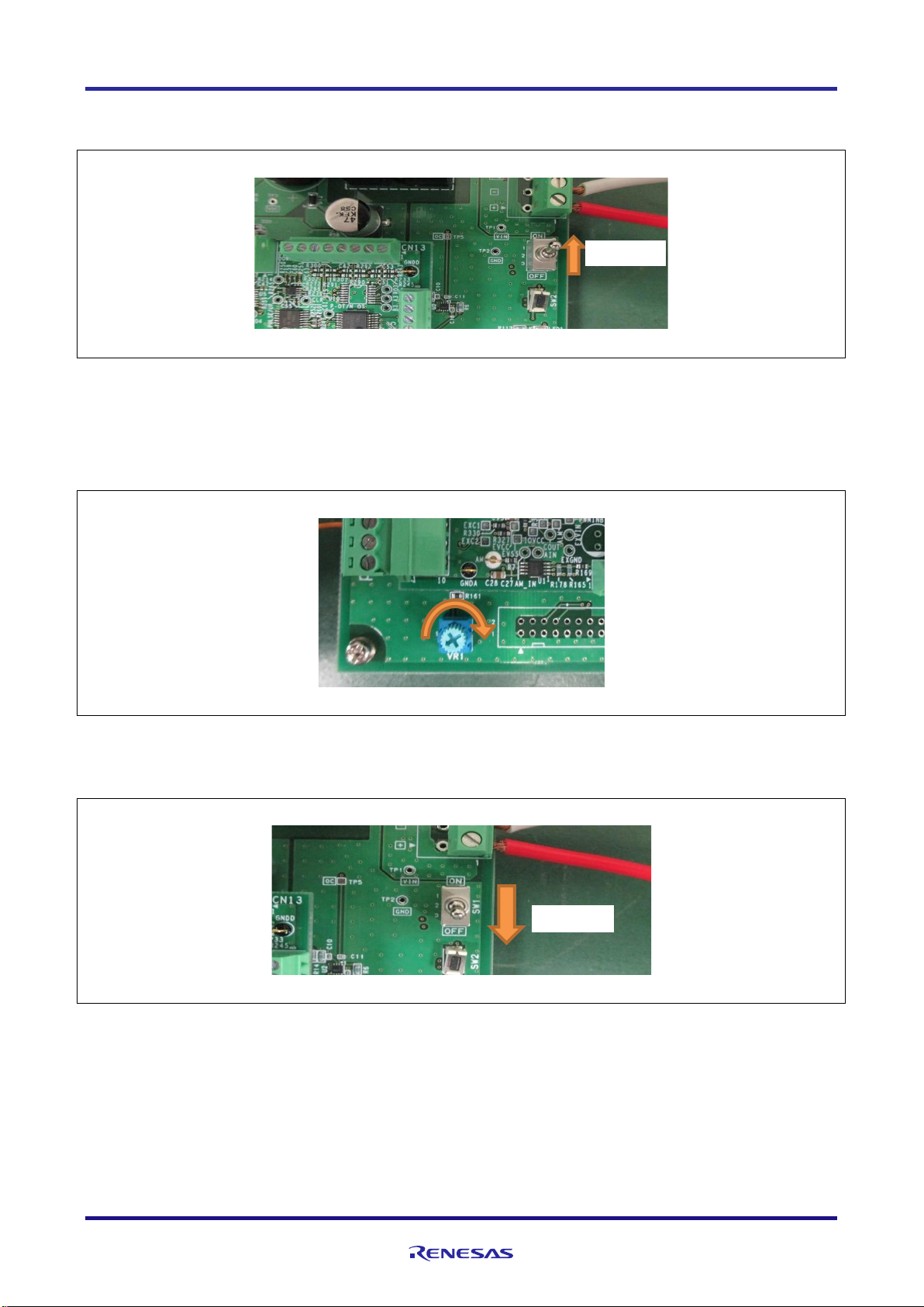
(2) Checking the SW1 and the variable resistor
While referencing Figure 2-3, check that the SW1 is OFF and the variable resistor (VR1) is in the center position. If
the VR1 is not in the center position, adjust it in the center position with an ESD safe slotted screwdriver.
Figure 2-3 Checking the SW1 and the Variable Resistor
Page 13
Evaluation System for Stepping Motor with Resolver User's Manual
R12UZ0065EJ0110 Rev.1.10 Page 13 of 54
2020.11.06
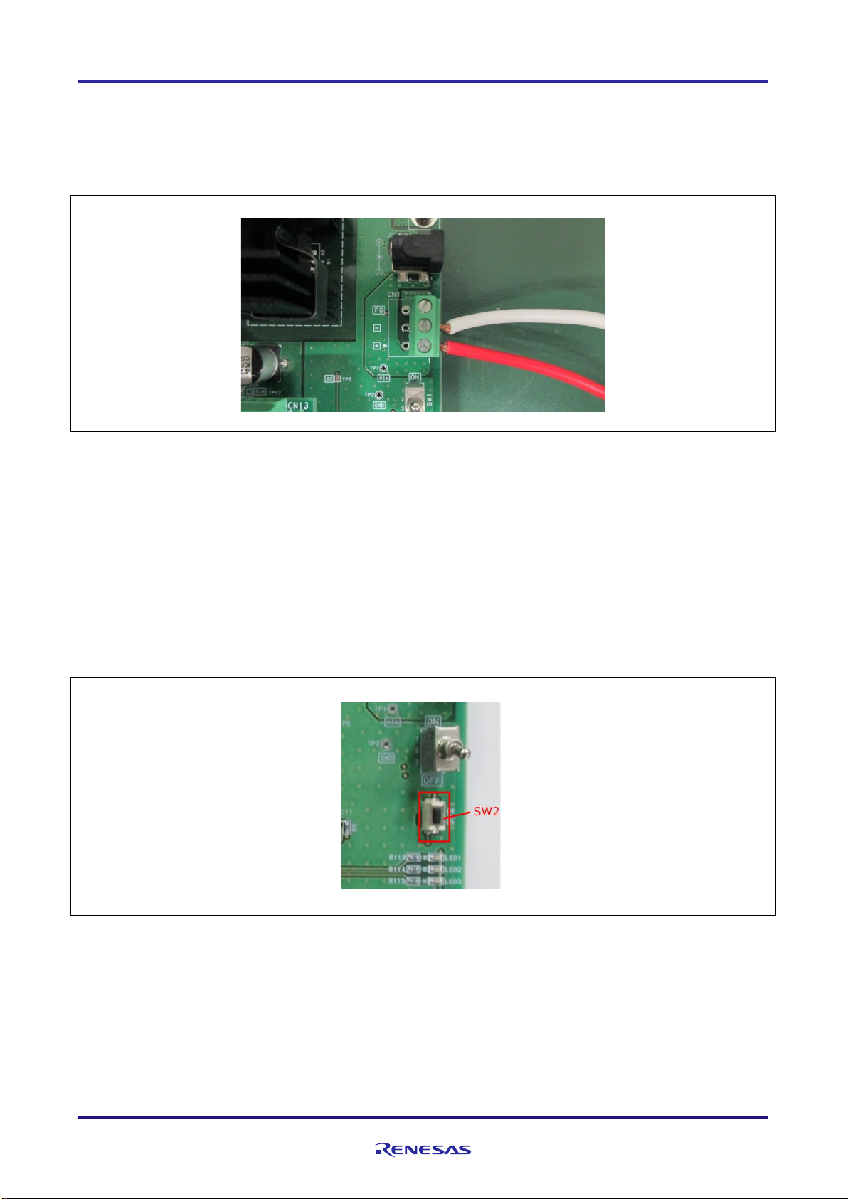
(3) Connecting the stabilized power supply and board
This product provides a terminal block and DC jack as connectors for supplying the power to the board. The
following explains an example of connecting the board to the terminal block using a stabilized power supply. Connect
the power supply to the board as shown in Figure 2-4.
Figure 2-4 Power supply to the power connector
(4) Supplying the power
Use a stabilized power supply as the power supply, set the output voltage to 24 V and the limit current to 1 A, and
start output. If the voltage drops even momentarily, a reset occurs since the voltage of the power supplied to the MCU
also drops, which causes the program to be halted.
(5) Executing the calibration
For calibratin the motor parmaters, push and release SW2 and wait for 30~40 seconds. The motor starts rotating in
20~30 seconds. It stops rotating when the calibration finishes.
Figure 2-5 Push SW2 for the Calibration
Page 14
Evaluation System for Stepping Motor with Resolver User's Manual
R12UZ0065EJ0110 Rev.1.10 Page 14 of 54
2020.11.06
(6) Enabling the rotation of the motor
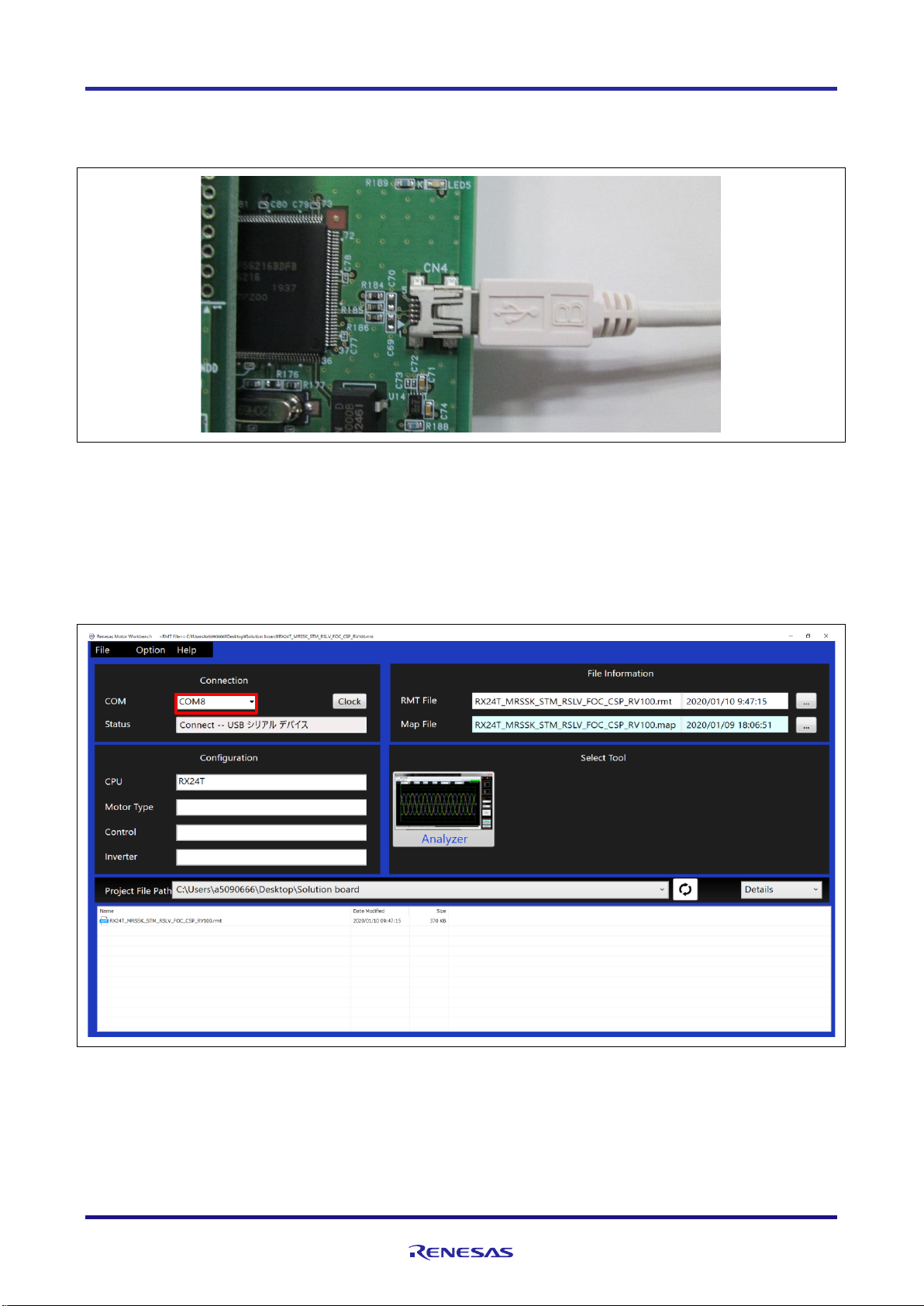
To enable the rotation of the motor, turn the toggle switch (SW1) on as shown in Figure 2-6.
Figure 2-6 Enabling the Rotation of the Motor
(7) Checking that the motor speed changes
Check that the motor speed changes when you turn the rotor of the variable resistor (VR1).
Figure 2-7 Changes of the Motor Speed
(8) Stopping the rotation of the motor
To stop the rotation of the motor, turn toggle switch SW1 off.
Figure 2-8 Stopping the Rotation of the Motor
(9) Stopping supplying the power
Check that the rotation stops and stop the output from the stabilized power supply.
SW1 ON
SW1 OFF
Page 15

Evaluation System for Stepping Motor with Resolver User's Manual
R12UZ0065EJ0110 Rev.1.10 Page 15 of 54
2020.11.06
2.2 Quick Start 2 GUI Operations
This section describes an operation procedure using Renesas Motor Workbench, support tool for motor control
development which is an application running on a PC.
Before starting this operation procedure, make connections and confirm SW setting according to steps (1) to (3) in
quick start 1. In addition, it is necessary to download the sample program “Vector Control of a Two-Phase Stepping
Motor Incorporating a Resolver Sensor”(R03AN0014) from the product page linked from the following URL and write
the program to the CPU card according to the procedure described in Chapter 4.
URL: http://japan.renesas.com/rssk/motor
Procedure of quick start 2
Step
Operation
(1)
Connecting a PC and this product
(2)
Connecting Renesas Motor Workbench
(3)
Loading the configuration file
(4)
Switching to the Analyzer tool
(5)
Changing the user interface
(6)
Executing offset calibration
(7)
Executing gain and phase calibration
(8)
Executing angle error calibration
(9)
Setting the command value of position control
(10)
Operating the motor in the position control mode
(11)
Turning the servo off
(12)
Sending a speed command
(13)
Stopping rotation
(14)
Stopping supplying the power
Page 16
Evaluation System for Stepping Motor with Resolver User's Manual
R12UZ0065EJ0110 Rev.1.10 Page 16 of 54
2020.11.06
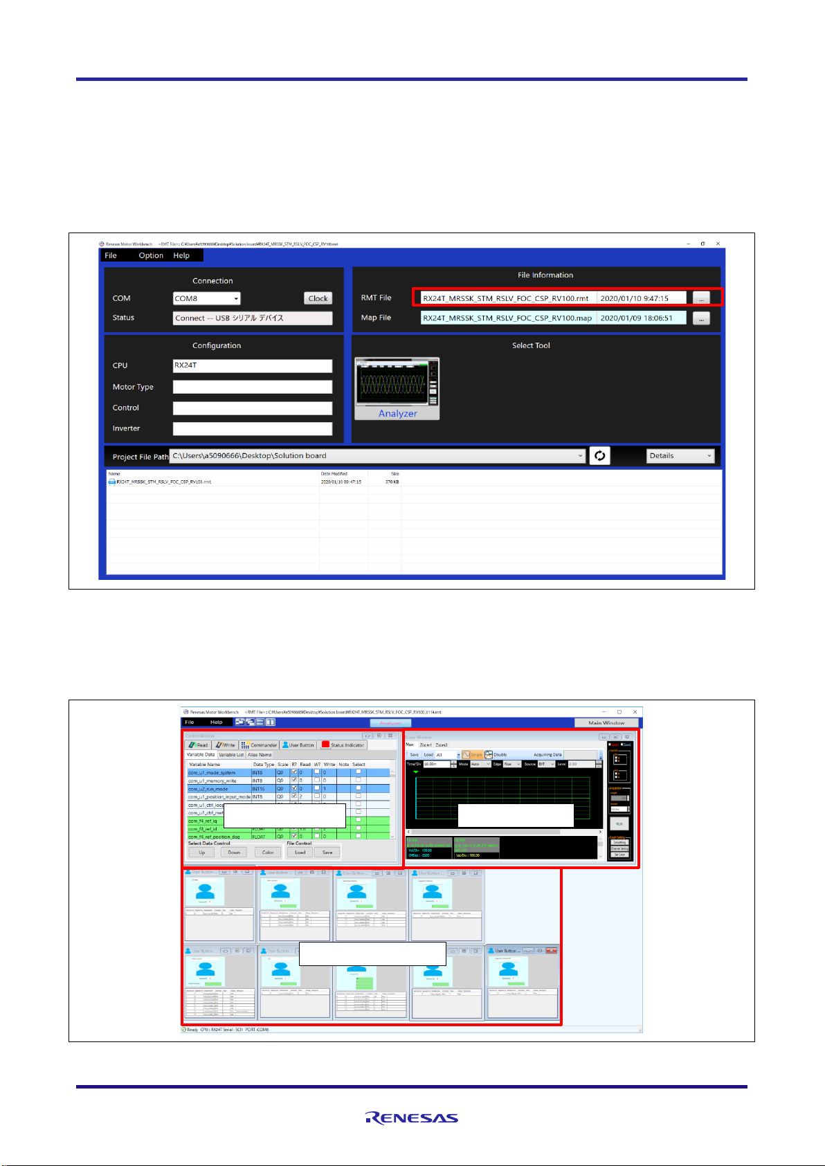
(1) Connecting a PC and this product
Connect the USB cable supplied with this product to the USB connector on a PC and USB connector CN4 on the
inverter board. After that, turn the power to the board on as instructed in step (4) of quick start 1.
Figure 2-9 Connecting a PC
(2) Connecting Renesas Motor Workbench
Start up Renesas Motor Workbench and check that the relevant COM number is displayed.
For details of the methods of RMW operations described below, refer to "Support Tool for Motor Control
Development, Renesas Motor Workbench User's Manual (R21UZ0004JJ)".
Figure 2-10 Checking the COM Number
Page 17
Evaluation System for Stepping Motor with Resolver User's Manual
R12UZ0065EJ0110 Rev.1.10 Page 17 of 54
2020.11.06
(3) Loading the configuration file
Download the sample code “Vector Control of a Two-Phase Stepping Motor Incorporating a Resolver
Sensor”(R03AN0014) and load the configuration file " RX24T_MRSSK_STM_RSLV_FOC_CSP_RVxxx.rmt " on
Renesas Motor Workbench.
Note that the capture screens in this manual may be different from the actual ones.
URL: http://japan.renesas.com/rssk/motor
Figure 2-11 Reading the Configuration File
(4) Switching to the Analyzer tool
In the Main window, click the Analyzer button. Renesas Motor Workbench displays the windows for the Analyzer
tool, Scope, User Button, and Control windows.
Figure 2-12 Display for the Renesas Motor Workbench Analyzer Tool
Scope window
Control window
User button window
Page 18
Evaluation System for Stepping Motor with Resolver User's Manual
R12UZ0065EJ0110 Rev.1.10 Page 18 of 54
2020.11.06
(5) Changing the user interface
Change the user interface from the switches and variable resistor on the board to Renesas Motor Workbench. On
Renesas Motor Workbench, click the "GUI mode" User Button. Variable com_u1_sw_userif is rewritten from 1 to 0
and the interface changes.
Figure 2-13 Changing the User Interface
(6) Executing offset calibration
Click the "Offset Calibration" User Button to execute offset calibration.
Figure 2-14 Starting the Execution of Offset Calibration
User Button "GUI mode"
Changes the user interface.
User Button "Offset Calibration"
Execute offset calibration.
Page 19

Evaluation System for Stepping Motor with Resolver User's Manual
R12UZ0065EJ0110 Rev.1.10 Page 19 of 54
2020.11.06
(7) Executing gain and phase calibration
Click the "Gain/Phase Calibration" User Button to execute gain and phase calibration.
Figure 2-15 Starting the Execution of Gain/Phase Calibration
(8) Executing angle error calibration
Click the "Angle error Calibration" User Button to execute angle error calibration. The motor starts rotating in 20~30
seconds. It stops rotating when the calibration finishes.
Figure 2-16 Starting the Execution of Angle Error Calibration
User Button " Gain/Phase Calibration"
Execute gain and phase calibration.
User Button " Angle error Calibration "
Execute angle error calibration.
Page 20

Evaluation System for Stepping Motor with Resolver User's Manual
R12UZ0065EJ0110 Rev.1.10 Page 20 of 54
2020.11.06
(9) Setting the command value of position control
Set the command value of position control in the "Position Control" User Button.
Figure 2-17 Write Command Value in the Position Control Mode
(10) Operating the motor in the position control mode
Click the "Position Control " User Button. The motor starts rotating and stops at the posision set in the step (9).
Figure 2-18 Position Control Mode
Write command
value "100".
User Button " Position Control "
The motor starts rotating and stops.
Expansion
Page 21

Evaluation System for Stepping Motor with Resolver User's Manual
R12UZ0065EJ0110 Rev.1.10 Page 21 of 54
2020.11.06
(11) Turning the servo off
Click the "Stop" User Button. The tool enters the stop mode from the position control mode and the servo is turned
off. (The motor shaft is released.)
Figure 2-19 Turning the Servo Off
(12) Sending a speed command
Click the "Speed Control" User Button. The motor rotates in the speed control mode and a waveform is displayed in
the Scope window.
Figure 2-20 Setting a Speed Command
User Button "Stop"
Puts the tool in the stop
mode.
User Button "Speed
Control"
Sends a speed
command.
The waveform in the
Scope window changes.
Push the "run" Button.
Page 22

Evaluation System for Stepping Motor with Resolver User's Manual
R12UZ0065EJ0110 Rev.1.10 Page 22 of 54
2020.11.06
(13) Stopping rotation
Click the "Stop" User Button. The motor stops.
Figure 2-21 Stopping the Motor
(14) Stopping supplying the power
Check that the rotation stops and stop the output from the stabilized power supply.
User Button "Stop"
Puts the tool in the stop
mode.
Page 23

Evaluation System for Stepping Motor with Resolver User's Manual
R12UZ0065EJ0110 Rev.1.10 Page 23 of 54
2020.11.06
2.3 Initial Software Specifications
Software for resolver vector control is factory-written on the RX24T. The specifications of the software are as
follows.
Table 2-1 Initial Software Specifications
Item
Specification
Control method
Resolver vector control
VR1
Turned clockwise: Rotates the motor counterclockwise.
Turned counterclockwise: Rotates the motor clockwise.
SW1
ON: Enables the rotation of the motor.
OFF: Disables the rotation of the motor.
SW2
Error occurs : cancels the error status
Motor rotates : N/A
Motor stops : calibration
LED1
On: SW1 in the ON state and normal operating status
Off: SW1 in the OFF state or error status
LED2
On: Error status
Off: Normal operating status
Renesas Motor Workbench
Available
Page 24

Evaluation System for Stepping Motor with Resolver User's Manual
R12UZ0065EJ0110 Rev.1.10 Page 24 of 54
2020.11.06
2.4 Writing to Flash Memory
Since this product has an on-board emulator circuit (flash programming circuit), you can write data to the flash
memory without separately preparing a tool product. Connect the supplied USB cable to CN17 (USB mini-B connector)
on the CPU card and the USB connector on the PC and write data using an application such as Renesas Flash
Programmer or e2studio. With Renesas Flash Programmer and e2studio, the on-board emulator circuit is recognized as
E2Lite. Make the connection setting for E2Lite.
For details of how to use each application, refer to the relevant user's manual.
Figure 2-22 Connecting the Cable
Page 25

Evaluation System for Stepping Motor with Resolver User's Manual
R12UZ0065EJ0110 Rev.1.10 Page 25 of 54
2020.11.06
2.5 Troubleshooting
・A connector is not mounted.
CN2, CN 4, CN 6, CN 7, CN 9, CN 11, CN 12, CN 13, and CN 14 are not mounted on the CPU card. Mount
required connectors.
・A cable is not connected (the number of connected cables is insufficient).
In the normal status, four motor cables and five resolver cables are connected.
・Some accessories are missing.
Check the accessory list. If any accessory is missing, contact the supplier from which you purchased this
product or Renesas Support.
・The motor does not operate.
Check whether power is supplied. Check whether the cable is connected.
・The rotation speed is unstable.
Execute auto calibration as instructed in quick start 2.
・The motor stops (the error status occurs).
Check whether the output current limitation of the power supply is proper. To rotate the supplied motor with
no load, set the current limitation to 1 A or higher. Also, see 2.5.1 and 2.5.2.
・This product cannot be connected with Renesas Motor Workbench (COM is not recognized).
Check that the version of Renesas Motor Workbench is 2.0 or later. When multiple COM numbers are
displayed, try to connect this product with another COM number.
・This product cannot be connected with Renesas Motor Workbench (The MCU (RX24T) is not recognized).
Check that the CPU card is correctly mounted on the inverter board and power is supplied to the inverter
board. The power to the CPU card is supplied from the inverter board.
・Software cannot be written to the MCU.
Check that the write setting is correct (see 2.4).
・Resetting this product to the factory settings
You can find the factory-set software in the product website. Download and write the software.
Page 26

Evaluation System for Stepping Motor with Resolver User's Manual
R12UZ0065EJ0110 Rev.1.10 Page 26 of 54
2020.11.06
2.5.1 When the Rotation of the Motor Stops
When the motor is driven, if any predetermined limit value is exceeded, the initial software assumes that an error
occurred, turns LED2 on the inverter board and CPU card, and stops the rotation.
To recover from the error, press SW2 when the toggle switch SW1 is in the OFF position. When the error status is
canceled, LED2 goes off.
Figure 2-23 Error Notification LED and SW2
2.5.2 Checking the Status (Renesas Motor Workbench)
If LED2 is still on even after you perform the operation described in 2.5.1, you can possibly find the cause by
checking the status with Renesas Motor Workbench. Click Read in the Control window of RMW to check the status.
The value of variable _g_st_foc.u2_error_status, which indicates the status may correspond to an error listed in Table
2-2.
Figure 2-24 Checking the Status in the Control Window
Table 2-2 Values of the Variable and Corresponding Error Statuses
Variable _g_st_foc.u2_error_status
Error status
0x0001
Overcurrent
0x0002
Overvoltage
Page 27

Evaluation System for Stepping Motor with Resolver User's Manual
R12UZ0065EJ0110 Rev.1.10 Page 27 of 54
2020.11.06
Kit Specifications
3.1 Specification List
Table 3-1 Specification List of the Evaluation System for Stepping Motor with Resolver
Major item
Item
Specification
MCU
Model name
R5F524TEADFP
Operation clock
20-MHz crystal oscillator (PLL-multiplied internal frequency: 80
MHz)
Power supply
Input voltage
24 VDC (-5%) to 48 VDC (+5%)
Connectors
・ Terminal block
・ DC jack (PL03B, center-positive)
Supplied motor
Type
Stepping motor
Size
42 mm square
Rated current
2 Apeak/phase
Holding torque
0.51 N m
Inverter circuit
Maximum output
100 W
Switching frequency
20 kHz or lower
Dead time
0.5 s or longer *1
PWM logic
Positive logic with both upper and lower arms
Current detection
Method
Voltage detection with a shunt resistor (-4 to +4 A)
Current detection method
Phase current detection (phase A, phase B)
Shunt resistor
25 m
Current detection amplifier
gain
Bain: 20
Bias: 2.5 V
A/D input range
0.25 to 4.75 V
(A/D input pin with an independent sample-and-hold circuit)
Sensors
Resolver
Method: Single-phase excitation two-phase output
Excitation frequency: 20 kHz
Encoder
Open-collector output, 200 kp/s applicable
Voltage detection
DC bus voltage detection
(Bus voltage detection)
Detection by resistance division
Phase voltage detection
Detection by resistance
Protection circuit
Overcurrent detection
When the current is 5 A, the overcurrent detection signal is
output and the inverter circuit stops*2.
Fuse
Rated current: 8 A
Reverse current
prevention diode
Repetitive peak reverse voltage: 75 V or higher
External device
interfaces
Communication interfaces
・ Renesas Motor Workbench communication circuit
・ RS-485 communication circuit
・ CAN communication circuit
Other interfaces
・ Pulse train command input circuit
・ General-purpose input/output circuits
User interfaces
Input
・ One toggle switch, one push switch
・ Variable resistor
Display
・ Three LEDs (Two of three are synchronized with LEDs on
the CPU card.)
・ LED for the power supply of the inverter control circuit
・ LED for the power supply of the CPU card
*1 It is not the dead time guaranteed with hardware. A dead time must be set with software. The dead time in the
initial program is factory-set to 0.5 s.
*2 To stop the inverter circuit, the POE function of the MCU is used.
Page 28

Evaluation System for Stepping Motor with Resolver User's Manual
R12UZ0065EJ0110 Rev.1.10 Page 28 of 54
2020.11.06
3.2 Stepping Motor with Resolver
Table 3-2 lists the specifications of the stepping motor with resolver in this product. Figure 3-1 shows the external
view of the motor.
Table 3-2 Specifications of the Stepping Motor with Resolver
Model No.
R17PMK440CNVA4438
Rated current (Apeak/Phase)
2.0
Winding resistance (ohm)
1.2
Holding torque (Nm)
0.51
Inductance (mH)
2.6
Rotor inertia (kgm2)
75.0
Detent torque (Nm)
0.017
Figure 3-1 External View of the Stepping Motor with Resolver
Figure 3-2 Motor and Resolver Cable Wiring
Page 29

Evaluation System for Stepping Motor with Resolver User's Manual
R12UZ0065EJ0110 Rev.1.10 Page 29 of 54
2020.11.06
3.3 Power Supply
To operate this product, it is necessary to apply 24 to 48 VDC externally. As connectors, the following items are
provided: Terminal block for connecting a stabilized power supply or switching power supply and a DC jack for
connecting an AC adapter. A voltage of 12 V for the gate driver and a voltage of 5 V for the MCU and other ICs are
generated on the inverter board.
A frame ground is provided on the terminal block. In addition, one of spacer mounting holes is connected to a frame
ground. When it is necessary to connect a frame ground, use either of them.
Figure 3-3 shows the connector. Table 3-3 lists the power input specifications. Table 3-4 lists the pin assignments of
the terminal block.
Figure 3-3 Power Connector
Table 3-3 Power Input Specifications
Power supply terminal block
DC jack
Input voltage
24 to 48 V 5%
24 V 5%
Input current
5 A (max)
3.5 A (max)
Applicable
cable
Cross section: 0.20 to 1.50 mm2
AWG: 16 to 30
Center-positive
Center diameter: 2 Barrel diameter: 6.5
Table 3-4 Power Supply Terminal Block
Connector
Signal name
Description
Inverter board CN1.1
VIN
Positive power input
Inverter board CN1.2
GND
Reference power input
Inverter board CN1.3
FG
Frame ground
A protection circuit is provided at the power input section, which consists of an overcurrent detection circuit,
overcurrent protection fuse, and reverse current prevention diode. The overcurrent detection circuit outputs the
overcurrent detection signal when the input current reaches 5 A. The rated current of the fuse is 8 A. Table 3-5 lists the
specifications of the protection circuit.
Table 3-5 Specifications of the Protection Circuit
Overcurrent detection threshold
5 A
Destinations of the overcurrent
detection signal
CNA.5, U2 (P70/POE0#) on the CPU card
Fuse characteristics
Rated current: 8 A. Blown at twice the
rated current within 5 seconds.
Page 30
Evaluation System for Stepping Motor with Resolver User's Manual
R12UZ0065EJ0110 Rev.1.10 Page 30 of 54
2020.11.06
3.4 Inverter Circuit
This product has an inverter circuit for driving a 2-phase stepping motor and a connector for connecting the motor.
3.4.1 Connector
The plug of the connector for connecting the motor is separated from the socket. The connector is located at the
position shown in Figure 3-4.
Figure 3-4 Connector for Connecting the Motor
Page 31

Evaluation System for Stepping Motor with Resolver User's Manual
R12UZ0065EJ0110 Rev.1.10 Page 31 of 54
2020.11.06
3.4.2 Inverter, Gate Driver
As the gate driver, the HIP4082 manufactured by Renesas Electronics Corporation is used. As the MOSFET, the
RJK1054DPB is used. Table 3-6 and Figure 3-5 show the configuration and connection of the inverter circuit.
Table 3-6 Inverter Drive Signal Board-to-Board Connection
CPU card
Board-to-
board
connector
Inverter board
Connection destination
(RX24T)
Gate driver
input
Gate driver
output
MOSFET
Motor pin
U2.56 (P71/MTIOC3B)
CNA.12
U4.7 (AHI)
U4.10 (AHO)
Q3
CN2.4
(phase A+)
U2.53 (P74/MTIOC3D)
CNA.9
U4.4 (ALI)
U4.13 (ALO)
Q4
U2.55 (P72/MTIOC4A)
CNA.11
U10.2 (BHI)
U10.16 (BHO)
Q5
CN2.3
(phase B+)
U2.52 (P75/MTIOC4C)
CNA.8
U10.3 (BLI)
U10.14 (BLO)
Q6
U2.45 (P95/MTIOC6B)
CNA.6
U4.2 (BHI)
U4.16 (BHO)
Q1
CN2.5
(phase A-)
U2.48 (P92/MTIOC6D)
CNA.4
U4.3 (BLI)
U4.14 (BLO)
Q2
U2.46 (P94/MTIOC7A)
CNA.10
U10.7 (AHI)
U10.10 (AHO)
Q7
CN2.2
(phase B-)
U2.49 (P91/MTIOC7C)
CNA.7
U10.4 (ALI)
U10.13 (ALO)
Q8
A
A
B
B
HIP4082A
+12V
AHO
ALO
FG
Inverter board
CPU card
RX24T
MTIOC3B
MTIOC3D
MTIOC4A
MTIOC4C
AA+
B+
B-
FG
HIP4082A
BHO
BLO
BHO
BLO
AHO
ALO
U4
MTIOC6D
MTIOC6B
MTIOC7A
MTIOC7C
BLI
BHI
ALI
AHI
ALI
AHI
U10
BLI
BHI
Q1
Q2
Q3
Q4
Q5
Q6
Q7
Q8
CN2
CNA
U2
Figure 3-5 Inverter Circuit
Page 32

Evaluation System for Stepping Motor with Resolver User's Manual
R12UZ0065EJ0110 Rev.1.10 Page 32 of 54
2020.11.06
3.4.3 Current Detection
This product has a current detection circuit for measuring the motor current. The current detection circuit converts
phase currents to voltage signals and inputs them to the A/D converter. Figure 3-6 shows the circuit configuration.
Table 3-7 shows the connection.
Inverter board
RX24T
ADC
CPU card
S&H
S&H
AN100
AN101
x20
2.5V Center
OUT
-IN
+IN
OUT
-IN
+IN
Motor
AA+
B+
B-
Q1
Q2
Q3
Q4
Q5
Q6
Q7
Q8
R27
R67
U5
U9
CNB
U2
CN2
Figure 3-6 Current Detection Circuit
Table 3-7 Motor Current Detection Signal Board-to-Board Connection
Inverter board
Board-to-
board
connector
CPU card
Measurement target
Current detection amplifier
Connection
destination (RX24T)
Input
Output
Phase A shunt R27+
U5.8 (IN+)
U5.5 (OUT)
CNB.5
U2.91
(P40/AN100)
Phase A shunt R27-
U5.1 (IN-)
CNB.3
Phase B shunt R67+
U9.8 (IN+)
U9.5 (OUT)
CNB.6
U2.89
(P41/AN101)
Phase B shunt R67-
U9.1 (IN-)
CNB.4
The relationship between the current value of the shunt resistor
in the current detection circuit and the A/D
conversion value
is expressed by Equation 1. Table 3-8 lists typical values.
Equation 1
A
Current value of the shunt resistor
Shunt resistance
G
V/V
Current detection amplifier gain
V
Analog supply voltage
LSB
A/D conversion value
Table 3-8 Motor Phase Current and Corresponding Output Voltage of the Current Detection Amplifier
Current value
4 A
2 A (rated)
0 A
-2 A (rated)
-4 A
Potential difference across
shunt resistor
0.2 V1%
0.1 V1%
0.0 V1%
-0.1 V1%
-0.2 V1%
Output voltage
4.5 V2%
3.5 V2%
2.5 V2%
1.5 V2%
0.5 V2%
A/D conversion value
(*1)
3685 LSB
2866 LSB
2048 LSB
1228 LSB
409 LSB
*1 Reference value in which the error of the A/D converter is not included
Page 33

Evaluation System for Stepping Motor with Resolver User's Manual
R12UZ0065EJ0110 Rev.1.10 Page 33 of 54
2020.11.06
3.4.4 Voltage Detection
This product has a voltage divider for measuring the supply voltage and voltage of each phase of the motor. The
output of the voltage divider is connected to the A/D converter on the RX24T. Figure 3-7 shows the circuit
configuration. Table 3-9 lists the connection destinations.
Inverter board
RX24T
ADC
CPU card
AN211
AN209
Motor
AA+
B+
B-
Q1
Q2
Q3
Q4
Q5
Q6
Q7
Q8
CNB
U2
CN2
AN208
AN207
AN210
S&H
Figure 3-7 Voltage Detection Circuit
Table 3-9 Voltage Detection Signal Board-to-Board Connection
Inverter board
Board-to-board
connector
CPU card
Measurement target
Connection destination
(RX24T: U2)
Inverter supply voltage
CNB.8
U2.78 (P55/AN211)
Phase A+ voltage
CNB.10
U2.82 (P51/AN207)
Phase B+ voltage
CNB.11
U2.81 (P52/AN208)
Phase B- voltage
CNB.12
U2.80 (P53/AN209)
Phase A- voltage
CNB.13
U2.79 (P54/AN210)
The relationship between the supply voltage and A/D conversion result is expressed by Equation 2. Table 3-10 lists
typical values.
Equation 2
V
Input voltage value
V
Analog supply voltage
LSB
A/D conversion value
Table 3-10 Relationships among the Input Voltage, Output Voltage, and A/D Conversion Value
Supply
voltage
A/D input
voltage
A/D conversion
value *1
24 V
1.077 V
882 LSB
36 V
1.616 V
1323 LSB
48 V
2.155 V
1765 LSB
*1 Reference value in which the error of the A/D convertor is not included
Page 34

Evaluation System for Stepping Motor with Resolver User's Manual
R12UZ0065EJ0110 Rev.1.10 Page 34 of 54
2020.11.06
3.5 Sensor Interfaces
3.5.1 Resolver
This product has a resolver/digital converter IC (RDC IC). The RDC IC converts the analog signal output from the
resolver to the phase-modulated digital signal output. For the specifications of the RDC IC, refer to "RDC IC User's
Manual (r03uz0002)".
The connector for connecting the resolver is of a plug/socket type, which allows you to connect and disconnect the
resolver easily. Figure 3-8 shows the location of the resolver connector supplied with this product. Table 3-11 lists
connection information of the resolver motor and resolver connector.
Figure 3-8 Connector for Connecting the Resolver
Table 3-11 Resolver Connector Connection
Connector
Signal
name
Connection destination
Resolver
cable color
CN10.1
cos-
RDC IC
U21.28 (EXCOUT2) via U21.17 (XBN) and R335
Black
CN10.2
EXOUT1
RDC IC
U21.26 (EXCOUT1) and U29 (EXCFBP) via R335
White
CN10.3
cos+
RDC IC
U21.28 (EXCOUT2) via U21.18 (XBP) and R335
Green
CN10.4
EXOUT1
RDC IC
U21.26 (EXCOUT1) and U29 (EXCFBP) via R335
-
CN10.5
sin+
RDC IC
U21.28 (EXCOUT2) via U21.23 (XAP) and R335
Red
CN10.6
EXOUT1
RDC IC
U21.26 (EXCOUT1) and U29 (EXCFBP) via R335
-
CN10.7
sin-
RDC IC
U21.28 (EXCOUT2) via U21.24 (XAN) and R335
Yellow
CN10.8
EXOUT1
RDC IC
U21.26 (EXCOUT1) and U29 (EXCFBP) via R335
-
CN10.9
shield
Power
supply
GND_A
-
CN10.10
shield
Power
supply
GND_A
-
Page 35

Evaluation System for Stepping Motor with Resolver User's Manual
R12UZ0065EJ0110 Rev.1.10 Page 35 of 54
2020.11.06
3.5.2 Encoder
This product supports encoder A/B/Z signal input. The signals are input to the MCU via the 5-V pull-up resistor, RC
filter, and buffer IC. Figure 3-9 shows the location of the encoder connector. Table 3-12 lists connection information of
the encoder and connector. Table 3-13 lists the specifications of the input signals. The connector is not mounted at the
factory. To use an encoder, mount a 2.54 mm pitch connector.
Figure 3-9 Encoder Connector
Table 3-12 Encoder Signal Connector Connection Information
Connector
Pin function
Connection destination (RX24T)
CN6.1
5 V
Power
supply
+5V_D
CN6.2
Phase A
RX24T
U2.58 (P33/MTCLKA)*1
CN6.3
GND
Power
supply
GND_D
CN6.4
Phase B
RX24T
U2.59 (P32/MTCLKB)*1
CN6.5
GND
Power
supply
GND_D
CN6.6
Phase Z
RX24T
U2.36 (PA5/MTIOC1A)*1
CN6.7
GND
Power
supply
GND_D
CN6.8
GND
Power
supply
GND_D
*1 Via the positive logic buffer IC
Table 3-13 Encoder Signal Input Specifications
Pulse rate
200 kp/r (max)
Input signal type
Open collector
Connector applicable wire
Cross section: 0.14 to 0.5 mm²
AWG: 20 to 26
Connector type
3.5 mm pitch plug/socket terminal block
Page 36

Evaluation System for Stepping Motor with Resolver User's Manual
R12UZ0065EJ0110 Rev.1.10 Page 36 of 54
2020.11.06
3.5.3 Origin/Limit Sensors
This product supports the photoelectric sensor signal input for origin/limit sensors. It has a pull-up resistor on the
board for supporting NPN sensors. The input signals are connected to the MCU all via the buffer IC. Figure 3-10 shows
the locations of the origin/limit sensor connectors. Table 3-14 lists the input specifications. Table 3-15 lists connector
connection information. The connectors are not mounted at the factory. To use a sensor, mount a 2.5 mm pitch
connector.
Figure 3-10 Origin/Limit Sensor Connectors
Table 3-14 Origin/Limit Sensor Input Specifications
Input signal type
Open collector
Connector
B3B-XH-A (J.S.T. Mfg. Co., Ltd.)
Table 3-15 Origin/Limit Sensor Signal Input Connector Connection Information
Connector
Signal
Connection destination
CN4.1
5V
+5V_D
CN4.2
DOG
U2.1 (PE5/IRQ0)*1
CN4.3
GND
GND_D
CN7.1
5V
+5V_D
CN7.2
N-OT
U2.7 (P00/IRQ2) *2
CN7.3
GND
GND_D
CN9.1
5V
+5V_D
CN9.2
P-OT
U2.7 (P00/IRQ2) *2
CN9.3
GND
GND_D
*1 Via the positive logic buffer IC
*2 A wired OR connection is made between N-OT and P-OT on the CPU card.
Page 37

Evaluation System for Stepping Motor with Resolver User's Manual
R12UZ0065EJ0110 Rev.1.10 Page 37 of 54
2020.11.06
3.6 External Device Interfaces
This product has various types of external device interfaces, which allows the connection of general motor control
devices.
3.6.1 Renesas Motor Workbench Communication Circuit
This product is equipped with a USB connection interface and supports support tool for motor control development
Renesas Motor Workbench (RMW). RMW, an application program running on a PC, can display internal variables of a
target microcontroller in waveform in real time, read and write them, and automatically extract each parameter. For
details of the operation method, refer to "RMW Operation Manual (r21uz0004)".
Figure 3-11 Renesas Motor Workbench Communication Circuit Connector
RX24T
Inverter board CPU card
Rene sas Motor
Workbench
communication
circuit
Digital Isolator
PD5/RXD1
PD3/TXD1
Power supply isolation
USB
Figure 3-12 Renesas Motor Workbench Communication Circuit
Page 38

Evaluation System for Stepping Motor with Resolver User's Manual
R12UZ0065EJ0110 Rev.1.10 Page 38 of 54
2020.11.06
3.6.2 RS-485 Communication
This product is equipped with an RS-485 communication interface, which enables asynchronous serial
communication using differential signals at a maximum of 5 Mbps. It also supports a multidrop system, which enables
control over transmission enable. For communication, the UART function built in the mounted MCU
(R5F524TEADFP) is used. As a transceiver, the ISL3156E manufactured by Renesas Electronics Corporation is
mounted. Figure 3-13 shows the location of the connector. Table 3-16 lists the communication specifications. Table
3-17 lists the connection information from the connector to the RX24T. The connector is not mounted at the factory. To
use RS-485 communication, mount a 2.54 mm pitch connector.
Figure 3-13 RS-485 Communication Connector
Table 3-16 RS-485 Communication Specifications
Baud rate
5 Mbps (max)
Half-/full-duplex
Full-duplex
Common-mode voltage
-7 to +12 V
Terminating resistor
100 , 0.1 F (AC termination)
ISL3156E
RS48 5
100
0.1u
RO
DI
Z
Y
A
B
DE
RE#
AC termination
Connector applicable wire
Cross section: 0.2 to 0.5 mm²
AWG: 20 to 24
Table 3-17 RS-485 Communication Connector Connection Information
Connector
Signal
Connection destination (RS-485
transceiver differential side)
CN12.1
Differential input +
RS-485 transceiver
U9.9 (A)
CN12.2
Differential input -
RS-485 transceiver
U9.8 (B)
CN12.3
GND
Power supply
-
CN12.4
Differential output -
RS-485 transceiver
U9.8 (Z)
CN12.5
Differential output +
RS-485 transceiver
U9.6 (Y)
Table 3-18 Connection between the RS-485 Transceiver and MCU
RS-485 transceiver CMOS level side
Connection with RX24T
Processing on the
board
U9.1 (RO)
U2.34 (PB1/RXD6)
10-k pull-up
U9.2 (RE#)
No connection with U2
10-k pull-down
U9.3 (DE)
U2.2 (P02)
10-k pull-down
U9.4 (DI)
U2.33 (PB2/TXD6)
-
Page 39

Evaluation System for Stepping Motor with Resolver User's Manual
R12UZ0065EJ0110 Rev.1.10 Page 39 of 54
2020.11.06
3.6.3 CAN Communication
This product is equipped with a CAN communication interface, which enables communication at a maximum of 1
Mbps. For communication, the RSCAN function built in the mounted MCU (R5F524TEADFP) is used. Figure 3-14
shows the location of the connector. Table 3-19 lists the communication specifications. Table 3-20 lists the connection
information from the connector to the RX24T. The connector is not mounted at the factory. To use CAN
communication, mount a 2.54 mm pitch connector.
Figure 3-14 CAN Communication Connector
Table 3-19 CAN Communication Specifications
Baud rate
1 Mbps (max)
Half-/full-duplex
Half-duplex
Terminating resistance
120
Connector applicable wire
Cross section: 0.2 to 0.5 mm²
AWG: 20 to 24
Table 3-20 CAN Communication Connection Information
Connector
Connection
destination
CN14.1
U13.6 (CANL)
CN14.2
GND
CN14.3
U13.7 (CANH)
Transceiver connection
destination
RX24T connection
destination
U13.1 (Txd)
U2.41 (PA0/CTXD0)
U13.4 (Rxd)
U2.40 (PA1/CRXD0)
Page 40

Evaluation System for Stepping Motor with Resolver User's Manual
R12UZ0065EJ0110 Rev.1.10 Page 40 of 54
2020.11.06
3.6.4 Pulse Train Command
This product is equipped with an input interface for pulse train commands, which enables the input of pulse train
commands at a maximum of 200 kp/r. The input signals are connected to the MCU all via the buffer IC. Figure 3-15
shows the location of the connector. Table 3-21 lists the input specifications. Table 3-22 lists connection information.
The connector is not mounted at the factory. To use pulse train commands, mount a 2.54 mm pitch connector.
Figure 3-15 Pulse Train Command Connector
Table 3-21 Pulse Train Command Input Specifications
Pulse rate
200 kp/r (max)
Input signal type
Open collector
Connector applicable wire
Cross section: 0.14 to 0.5 mm²
AWG: 20 to 26
Table 3-22 Pulse Train Command Input Connection Relationship
Connector
Signal name
Connection destination (RX24T)
CN13.1
5V
Power
supply
+5V_D
CN13.2
PULSE/UP
RX24T
U2.8 (PE4/MTCLKC)*1
CN13.3
GND
Power
supply
GND_D
CN13.4
DIR/DOWN
RX24T
U2.9 (PE3/MTCLKD)*1
CN13.5
GND
Power
supply
GND_D
CN13.6
CLR
RX24T
U2.38 (PA3/MTIOC2A)*1
CN13.7
GND
Power
supply
GND_D
CN13.8
GND
Power
supply
GND_D
*1 Via the positive logic buffer IC
Page 41

Evaluation System for Stepping Motor with Resolver User's Manual
R12UZ0065EJ0110 Rev.1.10 Page 41 of 54
2020.11.06
3.6.5 General-Purpose Output
This product has a general-purpose output interface for outputting various notification signals to external devices.
The interface has an open-collector buffer output with a withstand voltage of 30 V and is applicable for control devices
operating at 24 V. The output signals from the MCU are connected to the connector all via the buffer IC. Figure 3-16
shows the location of the connector. Table 3-23 lists the output specifications. Table 3-24 lists the connection
information. The connector is not mounted at the factory. To use the general-purpose output, mount a 2.54 mm pitch
connector.
Figure 3-16 General-Purpose Output Connector
Table 3-23 General-Purpose Output Specifications
Logic
Positive
Output type
Open collector
Withstand voltage
30 V
Connector applicable wire
Cross section: 0.14 to 0.5 mm²
AWG: 20 to 26
Table 3-24 General-Purpose Output Connector Connection Information
Connector
Signal name
Connection destination
(RX24T)
CN11.1
5V
Power
supply
+5V_D
CN11.2
General-purpose
output (RDY)
RX24T
U2.32 (PB3)*1
CN11.3
General-purpose
output (COIN)
RX24T
U2.27 (PB6) *1
CN11.4
General-purpose
output (ORG)
RX24T
U2.28 (PB5) *1
CN11.5
General-purpose
output (ERROR)
RX24T
U2.23 (PD2) *1
CN11.6
General-purpose
output
RX24T
U2.21 (PD4) *1
CN11.7
General-purpose
output
RX24T
U2.30 (PB4) *1
CN11.8
GND
Power
supply
GND_D
*1 Via the open-collector output IC with a withstand voltage of 30 V
Page 42

Evaluation System for Stepping Motor with Resolver User's Manual
R12UZ0065EJ0110 Rev.1.10 Page 42 of 54
2020.11.06
3.6.6 General-Purpose Input
This product has a general-purpose input interface for inputting various notification signals from external devices.
The interface has a pull-up circuit, assuming that open-collector signals are input. The input signals are connected to the
MCU all via the buffer IC. The connector is also used for the analog input. Figure 3-17 shows the location of the
connector. Table 3-25 lists the input specifications. Table 3-26 lists the connection information. The connector is not
mounted at the factory. To use the general-purpose input, mount a 2.54 mm pitch connector.
Figure 3-17 General-Purpose Input Connector
Table 3-25 General-Purpose Input Specifications
Logic
Positive
Input type
Pull-up/hysteresis input buffer
Withstand voltage
0 to 5 V
Connector applicable wire
Cross section: 0.14 to 0.5 mm²
AWG: 20 to 26
Table 3-26 General-Purpose Input Connector Connection Information
Connector
Signal name
Connection destination (RX24T)
CN2.4
GND
Power supply
GND_D
CN2.5
General-purpose
input
RX24T
U2.69 (P65)*1
CN2.6
General-purpose
input
RX24T
U2.26 (PB7)*1
CN2.7
General-purpose
input (SVON)
RX24T
U2.100 (P10)*1
CN2.8
5V
Power supply
+5V_D
*1 Via the positive logic buffer IC
Page 43

Evaluation System for Stepping Motor with Resolver User's Manual
R12UZ0065EJ0110 Rev.1.10 Page 43 of 54
2020.11.06
3.6.7 Analog Input
This product has an analog input circuit for inputting analog commands from external devices or general-purpose
analog signals. When the input end is open, a voltage of AVCC/2 = 2.5 V is input to the MCU. The connector is also
used for the general-purpose input. Figure 3-18 shows the location of the connector. Table 3-27 lists the input
specifications. Table 3-28 lists the connection information. The connector is not mounted at the factory. To use the
analog input, mount a 2.54 mm pitch connector.
Figure 3-18 Analog Input Connector
Table 3-27 Analog Input Specifications
Input voltage range [V]
0 to 5 V
Input characteristics
Two pull-up/pull-down resistors with a
resistance of 470 k 1%
When the input end is open: 2.5 V
CPU card
MCU
P64/AN204
1k
0.1u
470k
470k
Analog co mma nd
input
Connector applicable wire
Cross section: 0.14 to 0.5 mm²
AWG: 20 to 26
Table 3-28 Analog Input Connection Information
Connector
Signal name
Connection destination
CN2.1
GND
Power supply
GND_A
CN2.2
Analog input
RX24T
U2.70 (P64/AN204) *1
CN2.3
5V
Power supply
+5V_A
*1 Via the buffer configuration op-amp
Page 44

Evaluation System for Stepping Motor with Resolver User's Manual
R12UZ0065EJ0110 Rev.1.10 Page 44 of 54
2020.11.06
3.7 User Interfaces
3.7.1 LEDs
This product has four LEDs on the inverter board and three LEDs on the CPU card. Two LEDs on the CPU card are
connected to the same MCU pins to which LEDs on the inverter board are connected. Figure 3-19 shows the locations
of the LEDs. Table 3-29 lists the connection information.
Figure 3-19 LEDs
Table 3-29 LED On Conditions and Connection Information
LED
On condition
Off condition
Board-to-board
connector
Connection
destination
Inverter board: LED1
Port output: Low
Port output: High
CNA.1
CPU card: U2.97
(RX24T P81)
Inverter board: LED2
Port output: Low
Port output: High
CNA.2
CPU card: U2.98
(RX24T P80)
Inverter board: LED3
Port output: Low
Port output: High
CNA.3
CPU card: U2.39
(RX24T PA2)
Inverter board: LED4
5-V supplied
5-V supply stopped
-
5-V power supply
(+5V_D)
CPU card: LED1
Port output: Low
Port output: High
-
CPU card: U2.97
(RX24T P81)
CPU card: LED2
Port output: Low
Port output: High
-
CPU card: U2.98
(RX24T P80)
CPU card: LED3
5-V supplied
5-V supply stopped
-
5-V power supply
(+5V_D)
Page 45
Evaluation System for Stepping Motor with Resolver User's Manual
R12UZ0065EJ0110 Rev.1.10 Page 45 of 54
2020.11.06
3.7.2 Switches
This product has an MCU reset switch and two switches connected to MCU pin functions. Figure 3-20 shows the
locations of the switches. Table 3-30 lists the connection information.
Figure 3-20 Locations of the Switches
Table 3-30 Switch Input Levels and Connection Information
Switch
Switch type
Input
Board-to-board
connector
Connection
destination
Inverter board:
SW1
Toggle switch
Lever OFF position: High
Lever ON position: Low
CNA.13
CPU card: U2.76
(RX24T P61)
Inverter board:
SW2
Tact switch
Released: High
Pressed: Low
CNA.14
CPU card: U2.10
(RX24T P62)
CPU card: SW1
Tact switch
Released: High
Pressed: Low
-
CPU card: U2.10
(RX24T RES#)
3.7.3 Variable Resistor
This product has a variable resistor. Figure 3-21 shows the location. Table 3-31 lists the specifications.
Figure 3-21 Location of the Variable Resistor
Table 3-31 Specifications and Connection Information of the Variable Resistor
Output voltage range
0 to AVCC
Board-to-board connector
CNB.15
Connection destination
CPU card: U2.77 (RX24T P60/AN200)
Page 46
Evaluation System for Stepping Motor with Resolver User's Manual
R12UZ0065EJ0110 Rev.1.10 Page 46 of 54
2020.11.06
3.8 Pin Assignments
3.8.1 MCU Pin Function Assignments
Table 3-32 MCU Pin Function Assignments (1/3)
#
Port
Module
Function
IN/OUT
Connection destination
Signal name
1
PE5
ICU
IRQ0
IN
Sensor (origin)
DOG
2
P02
Port
P02
OUT
Upper device (RS-485)
RS485_DE-
3
VSS
Power
VSS
-
Power supply
GND_D
4
P00
ICU
IRQ2
IN
Sensor (limit)
N-OT, P-OT
5
VCL
Power
VCL
-
Power supply
VCL
6
MD
System
MD
IN/OUT
E2 on board
FINE
7
P01
POE
POE12#
IN
RDC IC
RDC_ALARM
8
PE4
MTU
MTCLKC
IN
Upper device (Pulse command)
PULSE/UP
9
PE3
MTU
MTCLKD
IN
Upper device (Pulse command)
DIR/DOWN
10
RES#
System
RES#
IN
Reset circuit/E2 on board
MCU_RESET
11
XTAL
System
XTAL
-
Oscillator
XTAL
12
VSS
Power
VSS
-
Power supply
GND_D
13
EXTAL
System
EXTAL
-
Oscillator
EXTAL
14
VCC
Power
VCC
-
Power supply
VCC_D
15
PE2
Not used
- - - - 16
PE1
Not used
- - - - 17
PE0
MTU9
MTIOC9B
OUT
RDC IC
CARRIER2
18
PD7
Not used
- - - - 19
PD6
RSPI
SSLA0
OUT
RDC IC
SPI_SCS
20
PD5
UART1
RXD1
IN
RMW communication circuit
ICS_RX
21
PD4
Port
PD4
OUT
Upper device (sequence output)
GPOUTPUT
22
PD3
UART1
TXD1
OUT
RMW communication circuit
ICS_TX
23
PD2
Port
PD2
OUT
Upper device (sequence output)
ERROR
24
PD1
Port
PD1
OUT
Sensor power ON/OFF
SPON
25
PD0
Not used
- - - - 26
PB7
Port
PB7
IN
Upper device (sequence input)
GPINPUT
27
PB6
Port
PB6
OUT
Upper device (sequence output)
COIN
28
PB5
Port
PB5
OUT
Upper device (sequence output)
ORG
29
VCC
Power
VCC
-
Power supply
VCC_D
30
PB4
Port
PB4
OUT
Upper device (sequence output)
GPOUTPUT
31
VSS
Power
VSS
-
Power supply
GND_D
32
PB3
Port
PB3
OUT
Upper device (sequence output)
RDY
33
PB2
UART6
TXD6
OUT
Upper device (RS-485)
RS485_TX
34
PB1
UART6
RXD6
IN
Upper device (RS-485)
RS485_RX
35
PB0
TMR
TMO0
OUT
RDC IC
PWMINA
36
PA5
MTU1
MTIOC1A
IN
Encoder
ENC_Z
37
PA4
RSPI
RSPCKA
OUT
RDC IC
SPI_SCLK
38
PA3
MTU2
MTIOC2A
IN
RDC IC
COUT
39
PA2
Port
PA2
OUT
LED
LED3#
40
PA1
RSCAN
CRXD0
IN
Upper device (CAN)
CAN_RX
Page 47

Evaluation System for Stepping Motor with Resolver User's Manual
R12UZ0065EJ0110 Rev.1.10 Page 47 of 54
2020.11.06
Table 3-33 MCU Pin Function Assignments (2/3)
#
Port
Module
Function
IN/OUT
Connection destination
Signal name
41
PA0
RSCAN
CTXD0
OUT
Upper device (CAN)
CAN_TX
42
VCC
Power
VCC
-
Power supply
VCC_D
43
P96
Not used
- - - - 44
VSS
Power
VSS
-
Power supply
GND_D
45
P95
MTU67
MTIOC6B
OUT
Gate driver
A-H
46
P94
MTU67
MTIOC7A
OUT
Gate driver
B-H
47
P93
Not used
- - - - 48
P92
MTU67
MTIOC6D
OUT
Gate driver
A-L
49
P91
MTU67
MTIOC7C
OUT
Gate driver
B-L
50
P90
Not used
- - - - 51
P76
Not used
- - - - 52
P75
MTU34
MTIOC4C
OUT
Gate driver
B+L
53
P74
MTU34
MTIOC3D
OUT
Gate driver
A+L
54
P73
Not used
- - - - 55
P72
MTU34
MTIOC4A
OUT
Gate driver
B+H
56
P71
MTU34
MTIOC3B
OUT
Gate driver
A+H
57
P70
POE
POE0#
IN
Overcurrent detection circuit
HISEDE_OC#
58
P33
MTU
MTCLKA
IN
Encoder phase A
ENC_A
59
P32
MTU
MTCLKB
IN
Encoder phase B
ENC_B
60
VCC
Power
VCC
-
Power supply
VCC_D
61
P31
MTU0
MTIOC0A
OUT
RDC IC
CC
62
VSS
Power
VSS
-
Power supply
GND_D
63
P30
Not used
- - - - 64
P24
D/A
DA0
OUT
Analog monitor
Analog_Mon
65
P23
RSPI
MOSIA
OUT
RDC IC
SPI_MOSI
66
P22
RSPI
MISOA
IN
RDC IC
SPI_MISO
67
P21
MTU9
MTIOC9A
OUT
RDC IC
CARRIER1
68
P20
Not used
-
- - -
69
P65
Port
P65
IN
Upper device (sequence
input/output)
GPINPUT
70
P64
A/D
AN204
IN
Upper device (analog command)
AIN
71
AVCC2
Power
AVCC2
-
Power supply
VCC_A
72
VREF
Power
VREF
-
Power supply
VCC_A
73
AVSS2
Power
AVSS2
-
Power supply
GND_A
74
P63
Not used
- - - - 75
P62
ICU
IRQ6
IN
Switch (tact)
SW2#
76
P61
ICU
IRQ5
IN
Switch (toggle)
SW1#
77
P60
A/D
AN200
IN
Variable resistor
VR1
78
P55
A/D
AN211
IN
Power supply detection
VDC
79
P54
A/D
AN210
IN
Phase voltage detection
VA-
80
P53
A/D
AN209
IN
Phase voltage detection
VB-
Page 48

Evaluation System for Stepping Motor with Resolver User's Manual
R12UZ0065EJ0110 Rev.1.10 Page 48 of 54
2020.11.06
Table 3-34 MCU Pin Function Assignments (3/3)
#
Port
Module
Function
IN/OUT
Connection destination
Signal name
81
P52
A/D
AN208
IN
Phase voltage detection
VB+
82
P51
A/D
AN207
IN
Phase voltage detection
VA+
83
P50
A/D
AN206
IN
RDC IC
MNTOUT_DC_1
84
P47
A/D
AN103
IN
RDC IC
MNTOUT_AC_1
85
P46
Not used
- - - - 86
P45
A/D
AN101
IN
Current detection amplifier
IB
87
P44
A/D
AN100
IN
Current detection amplifier
IA
88
P43
Port
P43
OUT
RDC IC
RDC_RESET
89
P42
Not used
- - -
90
P41
Not used
- - -
91
P40
Not used
- - - - 92
AVCC1
Power
AVCC1
-
Power supply
VCC_A
93
AVCC0
Power
AVCC0
-
Power supply
VCC_A
94
AVSS0
Power
AVSS0
-
Power supply
GND_A
95
AVSS1
Power
AVSS1
-
Power supply
GND_A
96
P82
TMR
TMO4
OUT
RDC IC
PWMINB
97
P81
Port
P81
OUT
LED1
LED1#
98
P80
Port
P80
OUT
LED2
LED2#
99
P11
TMR
TMO3
OUT
RDC IC
RDC_CLK
100
P10
Port
P10
IN
Upper device (sequence input)
SVON
Page 49

Evaluation System for Stepping Motor with Resolver User's Manual
R12UZ0065EJ0110 Rev.1.10 Page 49 of 54
2020.11.06
3.8.2 Board-to-Board Connector Pin Function Assignments
Table 3-35 Board-to-Board Connector CNA Connection Pins
#
Output
Signal
Connection destination
(inverter board)
Connection destination
(CPU card)
1
To INV
LED1#
LED1
U2.97 P81
2
To INV
LED2#
LED2
U2.98 P80
3
To INV
LED3#
LED3
U2.39 PA2
4
To INV
PWM phase A- L
Gate driver: U4.3 BLI
U2.48 P92/MTIOC6D
5
To CPU
Overcurrent
detection
Comparator output: U2.1
U2.57 P70/POE0#
6
To INV
PWM phase A- H
Gate driver: U4.2 BHI
U2.45 P95/MTIOC6B
7
To INV
PWM phase B- L
Gate driver: U10.4 ALI
U2.49 P91/MTIOC7C
8
To INV
PWM phase B+ L
Gate driver: U10.3 BLI
U2.52 P75/MTIOC4C
9
To INV
PWM phase A+ L
Gate driver: U4.4 ALI
U2.53 P74/MTIOC3D
10
To INV
PWM phase B- H
Gate driver: U10.7 AHI
U2.46 P94/MTIOC7A
11
To INV
PWM phase B+ H
Gate driver: U10.2 BHI
U2.55 P72/MTIOC4A
12
To INV
PWM phase A+ H
Gate driver: U4.7 AHI
U2.56 P71/MTIOC3B
13
To CPU
SW1
SW1
U2.76 P61
14
To CPU
SW2
SW2
U2.10 P62
15
To CPU
Digital 5V
+5V_D
+5V_D
16
To CPU
Digital 5V
+5V_D
+5V_D
17
To CPU
Digital GND
GND_D
GND_D
18
To CPU
Digital GND
GND_D
GND_D
19 - - - -
20 - - - -
Table 3-36 Board-to-Board Connector CNB Connection Pins
#
Output
Signal
Connection destination
(inverter board)
Connection destination
(CPU card)
1
To CPU
Analog 5V
+5V_A
+5V_A
2
To CPU
Analog 5V
+5V_A
+5V_A
3
To CPU
-
GND_A
- 4 To CPU
-
GND_A
-
5
To CPU
Phase A current
detection
Current detection amplifier:
U5.5
U2.91 P40/AN100
6
To CPU
Phase B current
detection
Current detection amplifier:
U9.5
U2.89 P41/AN101
7 - - - U2.85 P46
8
To CPU
Supply voltage divider
R2, R4
U2.78. P55/AN211
9
- - -
-
10
To CPU
Phase A+ voltage
divider
R32, R40
U2.82 P51/AN207
11
To CPU
Phase B+ voltage
divider
R72, R77
U2.81 P52/AN208
12
To CPU
Phase B- voltage
divider
R105, R108
U2.80 P53/AN209
13
To CPU
Phase A- voltage
divider
R12, R20
U2.79 P54/AN210
14 - - - U2.91 P40
15
To CPU
Volume
VR1
U2.77 P60/AN200
16 - - - -
17
To CPU
Digital 5V
+5V_D
+5V_D
18
To CPU
Digital 5V
+5V_D
+5V_D
19
To CPU
Analog ground
GND_A
GND_A
20
To CPU
Analog ground
GND_A
GND_A
Page 50

Evaluation System for Stepping Motor with Resolver User's Manual
R12UZ0065EJ0110 Rev.1.10 Page 50 of 54
2020.11.06
Table 3-37 Board-to-Board Connector CN10 Connection Pins
#
Output
Signal
Connection destination
(inverter board)
Connection
destination (CPU card)
1
To INV
RMW
communication:
Transmission
U13.3 A2
U2.22 PD3/TXD1
2 - Digital ground
GND_D
GND_D
3
To CPU
RMW
communication:
Reception
U13.2 A1
U2.20 PD5/RXD1
4 - Digital ground
GND_D
GND_D
Page 51

Evaluation System for Stepping Motor with Resolver User's Manual
R12UZ0065EJ0110 Rev.1.10 Page 51 of 54
2020.11.06
How to Flash Program MCU
This chapter describes how to write a sample program to MCU flash memory with e2studio. Download the sample
code “Vector Control of a Two-Phase Stepping Motor Incorporating a Resolver Sensor”(R03AN0014) from the product
page linked from the following URL.
URL: http://japan.renesas.com/rssk/motor
Note that the capture screens in this manual may be different from the actual ones.
(1) Connect CPU card to PC
Connect the supplied USB cable to CN17 (USB mini-B connector) on the CPU card and the USB connector on the
PC
Figure 4-1 Connecting the Cable
(2) Launch e2studio and import sample project
Import the sample project (for e2studio) into e2studio.
Figure 4-2 Import project
Page 52

Evaluation System for Stepping Motor with Resolver User's Manual
R12UZ0065EJ0110 Rev.1.10 Page 52 of 54
2020.11.06
(3) Configure Toolchain
Click the property of the project and configure the toolchain for your environment. The toolchains and versions you
can select depend on the installed toolchain in your e2studio.
Figure 4-3 Toolchain configuration
(4) Build project
Figure 4-4 Build project
Page 53

Evaluation System for Stepping Motor with Resolver User's Manual
R12UZ0065EJ0110 Rev.1.10 Page 53 of 54
2020.11.06
(5) Write the program into CPU card
Figure 4-5 Flash programming
(6) Disconnect CPU card from PC
Click disconnect and detach USB cable from the CPU card.
Figure 4-6 Disconnect CPU card
Page 54

Evaluation System for Stepping Motor with Resolver User's Manual
R12UZ0065EJ0110 Rev.1.10 Page 54 of 54
2020.11.06
Website and Support
Renesas Electronics Website
http://japan.renesas.com/
Inquiries
http://japan.renesas.com/contact/
All trademarks and registered trademarks are the property of their respective owners.
Page 55

Evaluation System for Stepping Motor with Resolver User's Manual
R12UZ0065EJ0110 Rev.1.10 Page 55 of 54
2020.11.06
Revision History
Rev.
Date
Description
Revised part
Summary
1.00
Nov. 29, 2019
-
First edition
1.10
Nov. 6, 2020
Added Section 4
Added how to flash program MCU
Page 56

General Precautions in the Handling of Microprocessing Unit and Microcontroller
Unit Products
The following usage notes are applicable to all Microprocessing unit and Microcontroller unit products from Renesas. For detailed usage notes on the products covered
by this document, refer to the relevant sections of the document as well as any technical updates that have been issued for the products.
1. Precaution against Electrostatic Discharge (ESD)
A strong electrical field, when exposed to a CMOS device, can cause destruction of the gate oxide and ultimately degrade the device operation. Steps must be taken to
stop the generation of static electricity as much as possible, and quickly dissipate it when it occurs. Environmental control must be adequate. When it is dry, a
humidifier should be used. This is recommended to avoid using insulators that can easily build up static electricity. Semiconductor devices must be stored and
transported in an anti-static container, static shielding bag or conductive material. All test and measurement tools including work benches and floors must be
grounded. The operator must also be grounded using a wrist strap. Semiconductor devices must not be touched with bare hands. Similar precautions must be taken for
printed circuit boards with mounted semiconductor devices.
2. Processing at power-on
The state of the product is undefined at the time when power is supplied. The states of internal circuits in the LSI are indeterminate and the states of register settings
and pins are undefined at the time when power is supplied. In a finished product where the reset signal is applied to the external reset pin, the states of pins are not
guaranteed from the time when power is supplied until the reset process is completed. In a similar way, the states of pins in a product that is reset by an on-chip
power-on reset function are not guaranteed from the time when power is supplied until the power reaches the level at which resetting is specified.
3. Input of signal during power-off state
Do not input signals or an I/O pull-up power supply while the device is powered off. The current injection that results from input of such a signal or I/O pull-up power
supply may cause malfunction and the abnormal current that passes in the device at this time may cause degradation of internal elements. Follow the guideline for
input signal during power-off state as described in your product documentation.
4. Handling of unused pins
Handle unused pins in accordance with the directions given under handling of unused pins in the manual. The input pins of CMOS products are generally in the highimpedance state. In operation with an unused pin in the open-circuit state, extra electromagnetic noise is induced in the vicinity of the LSI, an associated shootthrough current flows internally, and malfunctions occur due to the false recognition of the pin state as an input signal become possible.
5. Clock signals
After applying a reset, only release the reset line after the operating clock signal becomes stable. When switching the clock signal during program execution, wait
until the target clock signal is stabilized. When the clock signal is generated with an external resonator or from an external oscillator during a reset, ensure that the
reset line is only released after full stabilization of the clock signal. Additionally, when switching to a clock signal produced with an external resonator or by an
external oscillator while program execution is in progress, wait until the target clock signal is stable.
6. Voltage application waveform at input pin
Waveform distortion due to input noise or a reflected wave may cause malfunction. If the input of the CMOS device stays in the area between VIL (Max.) and VIH
(Min.) due to noise, for example, the device may malfunction. Take care to prevent chattering noise from entering the device when the input level is fixed, and also in
the transition period when the input level passes through the area between VIL (Max.) and VIH (Min.).
7. Prohibition of access to reserved addresses
Access to reserved addresses is prohibited. The reserved addresses are provided for possible future expansion of functions. Do not access these addresses as the
correct operation of the LSI is not guaranteed.
8. Differences between products
Before changing from one product to another, for example to a product with a different part number, confirm that the change will not lead to problems. The
characteristics of a microprocessing unit or microcontroller unit products in the same group but having a different part number might differ in terms of internal
memory capacity, layout pattern, and other factors, which can affect the ranges of electrical characteristics, such as characteristic values, operating margins, immunity
to noise, and amount of radiated noise. When changing to a product with a different part number, implement a system-evaluation test for the given product.
Page 57

Notice
1. Descriptions of circuits, software and other related information in this document are provided only to illustrate the operation of semiconductor products
and application examples. You are fully responsible for the incorporation or any other use of the circuits, software, and information in the design of your
product or system. Renesas Electronics disclaims any and all liability for any losses and damages incurred by you or third parties arising from the use
of these circuits, software, or information.
2. Renesas Electronics hereby expressly disclaims any warranties against and liability for infringement or any other claims involving patents, copyrights,
or other intellectual property rights of third parties, by or arising from the use of Renesas Electronics products or technical information described in this
document, including but not limited to, the product data, drawings, charts, programs, algorithms, and application examples.
3. No license, express, implied or otherwise, is granted hereby under any patents, copyrights or other intellectual property rights of Renesas Electronics
or others.
4. You shall not alter, modify, copy, or reverse engineer any Renesas Electronics product, whether in whole or in part. Renesas Electronics disclaims any
and all liability for any losses or damages incurred by you or third parties arising from such alteration, modification, copying or reverse engineering.
5. Renesas Electronics products are classified according to the following two quality grades: “Standard” and “High Quality”. The intended applications for
each Renesas Electronics product depends on the product’s quality grade, as indicated below.
"Standard": Computers; office equipment; communications equipment; test and measurement equipment; audio and visual equipment; home
electronic appliances; machine tools; personal electronic equipment; industrial robots; etc.
"High Quality": Transportation equipment (automobiles, trains, ships, etc.); traffic control (traffic lights); large-scale communication equipment; key
financial terminal systems; safety control equipment; etc.
Unless expressly designated as a high reliability product or a product for harsh environments in a Renesas Electronics data sheet or other Renesas
Electronics document, Renesas Electronics products are not intended or authorized for use in products or systems that may pose a direct threat to
human life or bodily injury (artificial life support devices or systems; surgical implantations; etc.), or may cause serious property damage (space
system; undersea repeaters; nuclear power control systems; aircraft control systems; key plant systems; military equipment; etc.). Renesas Electronics
disclaims any and all liability for any damages or losses incurred by you or any third parties arising from the use of any Renesas Electronics product
that is inconsistent with any Renesas Electronics data sheet, user’s manual or other Renesas Electronics document.
6. When using Renesas Electronics products, refer to the latest product information (data sheets, user’s manuals, application notes, “General Notes for
Handling and Using Semiconductor Devices” in the reliability handbook, etc.), and ensure that usage conditions are within the ranges specified by
Renesas Electronics with respect to maximum ratings, operating power supply voltage range, heat dissipation characteristics, installation, etc. Renesas
Electronics disclaims any and all liability for any malfunctions, failure or accident arising out of the use of Renesas Electronics products outside of such
specified ranges.
7. Although Renesas Electronics endeavors to improve the quality and reliability of Renesas Electronics products, semiconductor products have specific
characteristics, such as the occurrence of failure at a certain rate and malfunctions under certain use conditions. Unless designated as a high reliability
product or a product for harsh environments in a Renesas Electronics data sheet or other Renesas Electronics document, Renesas Electronics
products are not subject to radiation resistance design. You are responsible for implementing safety measures to guard against the possibility of bodily
injury, injury or damage caused by fire, and/or danger to the public in the event of a failure or malfunction of Renesas Electronics products, such as
safety design for hardware and software, including but not limited to redundancy, fire control and malfunction prevention, appropriate treatment for
aging degradation or any other appropriate measures. Because the evaluation of microcomputer software alone is very difficult and impractical, you are
responsible for evaluating the safety of the final products or systems manufactured by you.
8. Please contact a Renesas Electronics sales office for details as to environmental matters such as the environmental compatibility of each Renesas
Electronics product. You are responsible for carefully and sufficiently investigating applicable laws and regulations that regulate the inclusion or use of
controlled substances, including without limitation, the EU RoHS Directive, and using Renesas Electronics products in compliance with all these
applicable laws and regulations. Renesas Electronics disclaims any and all liability for damages or losses occurring as a result of your noncompliance
with applicable laws and regulations.
9. Renesas Electronics products and technologies shall not be used for or incorporated into any products or systems whose manufacture, use, or sale is
prohibited under any applicable domestic or foreign laws or regulations. You shall comply with any applicable export control laws and regulations
promulgated and administered by the governments of any countries asserting jurisdiction over the parties or transactions.
10. It is the responsibility of the buyer or distributor of Renesas Electronics products, or any other party who distributes, disposes of, or otherwise sells or
transfers the product to a third party, to notify such third party in advance of the contents and conditions set forth in this document.
11. This document shall not be reprinted, reproduced or duplicated in any form, in whole or in part, without prior written consent of Renesas Electronics.
12. Please contact a Renesas Electronics sales office if you have any questions regarding the information contained in this document or Renesas
Electronics products.
(Note1) “Renesas Electronics” as used in this document means Renesas Electronics Corporation and also includes its directly or indirectly controlled
subsidiaries.
(Note2) “Renesas Electronics product(s)” means any product developed or manufactured by or for Renesas Electronics.
(Rev.4.0-1 November 2017)
Corporate Headquarters
Contact information
TOYOSU FORESIA, 3-2-24 Toyosu,
Koto-ku, Tokyo 135-0061, Japan
www.renesas.com
For further information on a product, technology, the most up-to-date
version of a document, or your nearest sales office, please visit:
www.renesas.com/contact/.
Trademarks
Renesas and the Renesas logo are trademarks of Renesas Electronics
Corporation. All trademarks and registered trademarks are the property
of their respective owners.
 Loading...