

Page 1

User’s Manual
78K0/Fx2-L
8
User’s Manual: Hardware
8-Bit Single-Chip Microcontrollers
All information contained in these materials, including products and product specifications,
represents information on the product at the time of publication and is subject to change by
Renesas Electronics Corp. without notice. Please review the latest information published by
Renesas Electronics Corp. through various means, including the Renesas Electronics Corp.
website (http://www.renesas.com).
www.renesas.com
Rev.2.03 Jun 2012
Page 2

Notice
1. Descriptions of circuits, software and other related information in this document are provided only to illustrate the operation of
semiconductor products and application examples. You are fully responsible for the incorporation of these circuits, software,
and information in the design of your equipment. Renesas Electronics assumes no responsibility for any losses incurred by you
or third parties arising from the use of these circuits, software, or information.
2. Renesas Electronics has used reasonable care in preparing the information included in this document, but Renesas Electronics
does not warrant that such information is error free. Renesas Electronics assumes no liability whatsoever for any damages
incurred by you resulting from errors in or omissions from the information included herein.
3. Renesas Electronics does not assume any liability for infringement of patents, copyrights, or other intellectual property rights of
third parties by or arising from the use of Renesas Electronics products or technical information described in this document. No
license, express, implied or otherwise, is granted hereby under any patents, copyrights or other intellectual property rights of
Renesas Electronics or others.
4. You should not alter, modify, copy, or otherwise misappropriate any Renesas Electronics product, whether in whole or in part.
Renesas Electronics assumes no responsibility for any losses incurred by you or third parties arising from such alteration,
modification, copy or otherwise misappropriation of Renesas Electronics product.
5. Renesas Electronics products are classified according to the following two quality grades: “Standard” and “High Quality”. The
recommended applications for each Renesas Electronics product depends on the product’s quality grade, as indicated below.
“Standard”: Computers; office equipment; communications equipment; test and measurement equipment; audio and visual
equipment; home electronic appliances; machine tools; personal electronic equipment; and industrial robots etc.
“High Quality”: Transportation equipment (automobiles, trains, ships, etc.); traffic control syst ems; anti-disaster systems; anti-
crime systems; and safety equipment etc.
Renesas Electronics products are neither intended nor authorized for use in products or systems that may pose a direct threat to
human life or bodily injury (artificial life support devices or systems, surgical implantations etc.), or may cause serious property
damages (nuclear reactor control systems, military equipment etc.). You must check the quality grade of each Renesas
Electronics product before using it in a particular application. You may not use any Renesas Electronics product for any
application for which it is not intended. Renesas Electronics shall not be in any way liable for any damages or losses incurred
by you or third parties arising from the use of any Renesas Electronics product for which the product is not intended by Renesas
Electronics.
6. You should use the Renesas Electronics products described in this document within the range specified by Renesas Electronics,
especially with respect to the maximum rating, operating supply voltage range, movement power voltage range, heat radiation
characteristics, installation and other product characteristics. Renesas Electronics shall have no liability for malfunctions or
damages arising out of the use of Renesas Electronics products beyond such specified ranges.
7. Although Renesas Electronics endeavors to improve the quality and reliability of its products, semiconductor products have
specific characteristics such as the occurrence of failure at a certain rate and malfunctions under certain use conditions. Further,
Renesas Electronics products are not subject to radiation resistance design. Please be sure to implement safety measures to
guard them against the possibility of physical injury, and injury or damage caused by fire in the event of the failure of a Renesas
Electronics product, such as safety design for hardware and software including but not limited to redundancy, fire control and
malfunction prevention, appropriate treatment for aging degradation or any other appropriate measures. Because the evaluation
of microcomputer software alone is very difficult, please evaluate the safety of the final products or systems manufactured by
you.
8. Please contact a Renesas Electronics sales office for details as to environmental matters such as the environmental compatibility
of each Renesas Electronics product. Please use Renesas Electronics products in compliance with all applicable laws and
regulations that regulate the inclusion or use of controlled substances, including without limitation, the EU RoHS Directive.
Renesas Electronics assumes no liability for damages or losses occurring as a result of your noncompliance with applicable laws
and regulations.
9. Renesas Electronics products and technology may not be used for or incorporated into any products or systems whose
manufacture, use, or sale is prohibited under any applicable domestic or foreign laws or regulations. You should not use
Renesas Electronics products or technology described in this document for any purpose relating to military applications or use
by the military, including but not limited to the development of weapons of mass destruction. When exporting the Renesas
Electronics products or technology described in this document, you should comply with the applicable export control laws and
regulations and follow the procedures required by such laws and regulations.
10. It is the responsibility of the buyer or distributor of Renesas Electronics products, who distributes, disposes of, or otherwise
places the product with a third party, to notify such third party in advance of the contents and conditions set forth in this
document, Renesas Electronics assumes no responsibility for any losses incurred by you or third parties as a result of
unauthorized use of Renesas Electronics products.
11. This document may not be reproduced or duplicated in any form, in whole or in part, without prior written consent of Renesas
Electronics.
12. Please contact a Renesas Electronics sales office if you have any questions regarding the information contained in this document
or Renesas Electronics products, or if you have any other inquiries.
(Note 1) “Renesas Electronics” as used in this document means Renesas Electronics Corporation and also includes its majority-
owned subsidiaries.
(Note 2) “Renesas Electronics product(s)” means any product developed or manufactured by or for Renesas Electronics.
(2012.4)
Page 3

NOTES FOR CMOS DEVICES
(1) VOLTAGE APPLICATION WAVEFORM AT INPUT PIN: Waveform distortion due to input noise or a
reflected wave may cause malfunction. If the input of the CMOS device stays in the area between VIL
(MAX) and VIH (MIN) due to noise, etc., the device may malfunction. Take care to prevent chattering noise
from entering the device when the input level is fixed, and also in the tra nsition period when the input level
passes through the area between VIL (MAX) and VIH (MIN).
(2) HANDLING OF UNUSED INPUT PINS: Unconnected CMOS device inputs can be cause of malfunction. If
an input pin is unconnected, it is possible that an internal input level may be generate d due to noise, etc.,
causing malfunction. CMOS devices behave differently than Bipolar or NMOS devices. Input levels of
CMOS devices must be fixed high or low by using pull-up or pull-do wn circuitry. Each unused pin should be
connected to VDD or GND via a resistor if there is a possibility that it will be an output pin. All handling
related to unused pins must be judged separately for each device and according to related specifications
governing the device.
(3) PRECAUTION AGAINST ESD: A strong electric field, when exposed to a MOS device, can cause
destruction of the gate oxide and ultimately degrade the device operation. Steps must be taken to stop
generation of static electricity as much as possible, and quickly dissipate it when it has occurred.
Environmental control must be adequate. When it is dry, a humidifier should b e used. It is recommended
to avoid using insulators that easily build up static electricity. Semiconductor devices must be stored and
transported in an anti-static container, static shielding bag or conductive material. All test and measurement
tools including work benches and floors should be grounded. The operator should be gr oun ded usin g a wrist
strap. Semiconductor devices must not be touched with bare hands. Similar precautions need to be taken
for PW boards with mounted semiconductor devices.
(4) STATUS BEFORE INITIALIZATION: Power-on does not necessarily define the initial status of a MOS
device. Immediately after the power source is turned ON, devices with reset functions have not yet been
initialized. Hence, power-on does not guarantee output pin levels, I/O settings or contents of registers. A
device is not initialized until the reset signal is received. A reset operation must be executed immediately
after power-on for devices with reset functions.
(5) POWER ON/OFF SEQUENCE: In the case of a device that uses different power supplies for the internal
operation and external interface, as a rule, switch on the e xternal power suppl y after switching on th e internal
power supply. When switching the power supply off, as a rule, switch off the external power supply and then
the internal power supply. Use of the reverse po wer on/off sequences may result in the application of an
overvoltage to the internal elements of the device, causing malfunction and degr adation of internal elements
due to the passage of an abnormal current. The correct po wer on/off sequence must be judged separately
for each device and according to related specifications governing the device.
(6) INPUT OF SIGNAL DURING POWER OFF STATE : Do not input signals or an I/O pull-up power supply
while the device is not powered. The current injection that results from input of such a signal or I/O pull-up
power supply may cause malfunction and the abnormal current that passes in the device at this time may
cause degradation of internal elements. Input of signals during the power off state must be judged
separately for each device and according to related specifications governing the device.
Page 4

How to Use This Manual
Readers This manual is intended for user engineers who wish to understand the functions of the
78K0/Fx2-L microcontrollers and design and develop application system s and programs for
these devices.
The target products are as follows.
• 78K0/FY2-L:
• 78K0/FA2-L:
• 78K0/FB2-L:
Purpose This manual is intended to give users an understanding of the functions described in the
Organization below.
Organization The manual for the 78K0/Fx2-L microcontrollers is separated into two parts: this manual
and the instructions edition (common to the 78K0 microcontrollers).
μ
PD78F0854, 78F0855, 78F0856
μ
PD78F0857, 78F0858, 78F0859
μ
PD78F0864, 78F0865
78K0/Fx2-L
User’s Manual
(This Manual)
78K/0 Series
User’s Manual
Instructions
• Pin functions
• Internal block functions
• Interrupts
• Other on-chip peripheral functions
• Electrical specifications
How to Read This Manual It is assumed that the readers of this manual have general knowledge of electrical
engineering, logic circuits, and microcontrollers.
• To gain a general understanding of functions:
→ Read this manual in the order of the CONTENTS. The mark “<R>” shows major
revised points. The revised points can be easily searched by copying an “<R>” in the
PDF file and specifying it in the “Find what.” field.
• How to interpret the register format:
→ For a bit number enclosed in angle brackets, the bit name is defined as a reserved
word in the RA78K0, and is defined as an sfr variable using the #pragma sfr directive
in the CC78K0.
• To know details of the 78K0 microcontroller instructions:
→ Refer to the separate document 78K/0 Series Instructions User’s Manual
(U12326E).
Conventions Data significance: Higher digits on the left and lower digits on the right
Active low representations: ××× (overscore over pin and signal name)
Note: Footnote for item marked with Note in the text
Caution: Information requiring particular attention
Remark: Supplementary information
Numerical representations: Binary
Decimal
Hexadecimal
• CPU functions
• Instruction set
• Explanation of each instruction
...
×××× or ××××B
...
××××
...
××××H
Page 5

Related Documents The related documents indicated in this publication may include preliminary versions.
However, preliminary versions are not marked as such.
Documents Related to Devices
Document Name Document No.
78K0/Fx2-L User’s Manual U19856E
78K/0 Series Instructions User’s Manual U12326E
78K0 Microcontrollers User’s Manual Self Programming Library Type 01 U18274E
78K0 Microcontrollers Self Programming Library Type 01 Ver. 3.10 Operating Precautions (Notification
Document)
78K0 Microcontrollers User’s Manual EEPROM™ Emulation Library Type 01
78K0 Microcontrollers EEPROM Emulation Library Type 01 Ver.2.10 Operating Precautions (Notification
Document)
ZUD-CD-09-0122-E
U18275E
ZUD-CD-09-0165-E
Documents Related to Development Tools (Hardware) (User’ s Manual)
Document Name Document No.
QB-78K0FX2L In-Circuit Emulator To be prepared
QB-MINI2 On-Chip Debug Emulator with Programming Function U18371E
QB-Programmer Programming GUI Operation U18527E
Documents Related to Flash Memory Programming (User’s Manual)
Document Name Document No.
PG-FP5 Flash Memory Programmer U18865E
Caution The related documents listed above are subject to change without notice. Be sure to use the latest
version of each document for designing.
Page 6

Documents Related to Development Tools (Software)
Document Name Document No.
Note 1
Operation U17199E
Language U17198E
Structured Assembly Language U17197E
Note 1
Operation U17201E
Language U17200E
Note 2
Operation U18601E SM+ System Simulator User’s Manual
User Open Interface U18212E
ZUD-CD-07-0181-E
ZUD-CD-07-0103-E
U16934E
U18416E
RA78K0 Ver.3.80 Assembler Package User’s Manual
78K0 Assembler Package RA78K0 Ver.4.01 Operating Precautions (Notification Document)
CC78K0 Ver.3.70 C Compiler User’s Manual
78K0 C Compiler CC78K0 Ver. 4.00 Operating Precautions (Notification Document)
ID78K0-QB Ver.2.94 Integrated Debugger User’s Manual Operation U18330E
ID78K0-QB Ver.3.00 Integrated Debugger User’s Manual Operation U18492E
PM plus Ver.5.20
PM+ Ver.6.30
Note 3
Note 4
User’s Manual
User’s Manual
Note 2
Notes 1. This document is installed into the PC together with the tool when installing RA78K0 Ver. 4.01. For
descriptions not included in “78K0 Assembler Package RA78K0 Ver. 4.01 Operating Prec autions”, refer to the
user’s manual of RA78K0 Ver. 3.80.
2. This document is installed into the PC together with the tool when installing CC78K0 Ver. 4.00. For
descriptions not included in “78K0 C Compiler CC78K0 Ver. 4.00 Operating Precautions”, refer to the user’s
manual of CC78K0 Ver. 3.70.
3. PM plus Ver. 5.20 is the integrated development environment included with RA78K0 Ver. 3.80.
4. PM+ Ver. 6.30 is the integrated development environment included with RA78K0 Ver. 4.01. Software tool
(assembler, C compiler, debugger, and simulator) products of different versions can be managed.
Other Documents
Document Name Document No.
SEMICONDUCTOR SELECTION GUIDE − Products and Packages − X13769X
Semiconductor Device Mount Manual Note
Quality Grades on NEC Semiconductor Devices C11531E
NEC Semiconductor Device Reliability/Quality Control System C10983E
Guide to Prevent Damage for Semiconductor Devices by Electrostatic Discharge (ESD) C11892E
Note See the “Semiconductor Device Mount Manual” website (http://www2.renesas.com/pkg/en/mount/index.html).
Caution The related documents listed above are subject to change without notice. Be sure to use the latest
version of each document when designing.
All trademarks and registered trademarks are the property of their respective owners.
EEPROM is a trademark of Renesas Electronics Corporation.
Windows is a registered trademark or trademark of Microsoft Corporation in the United States and/or other countries.
SuperFlash is a registered trademark of Silicon Storage Technology, Inc. in several countries including the United States
and Japan.
®
Caution: This product uses SuperFlash
technology licensed from Silicon Storage Technology, Inc.
Page 7

CONTENTS
CHAPTER 1 OUTLINE.............................................................................................................................15
1.1 Features......................................................................................................................................... 15
1.2 Ordering Information....................................................................................................................17
1.3 Pin Configuration (Top View)......................................................................................................19
1.3.1 78K0/FY2-L (16 pins)......................................................................................................................... 19
1.3.2 78K0/FA2-L (20 pins)......................................................................................................................... 20
1.3.3 78K0/FB2-L (30 pins)......................................................................................................................... 21
1.4 Block Diagram .............................................................................................................................. 22
1.4.1 78K0/FY2-L (16 pins)......................................................................................................................... 22
1.4.2 78K0/FA2-L (20 pins)......................................................................................................................... 23
1.4.3 78K0/FB2-L (30 pins)......................................................................................................................... 24
1.5 Outline of Functions.....................................................................................................................25
CHAPTER 2 PIN FUNCTIONS...............................................................................................................27
2.1 Pin Function List .......................................................................................................................... 27
2.1.1 78K0/FY2-L ....................................................................................................................................... 28
2.1.2 78K0/FA2-L ....................................................................................................................................... 30
2.1.3 78K0/FB2-L ....................................................................................................................................... 32
2.2 Description of Pin Functions ...................................................................................................... 35
2.2.1 P00 to P02 (port 0) ............................................................................................................................ 35
2.2.2 P20 to P27 (port 2) ............................................................................................................................ 36
2.2.3 P30 to P37 (port 3) ............................................................................................................................ 37
2.2.4 P60 and P61 (port 6) ......................................................................................................................... 39
2.2.5 P70 (port 7)........................................................................................................................................ 40
2.2.6 P121 and P122 (port 12) ................................................................................................................... 40
2.2.7 AVREF, AVSS, VDD, VSS........................................................................................................................ 42
2.2.8 RESET............................................................................................................................................... 42
2.2.9 REGC................................................................................................................................................42
2.3 Pin I/O Circuits and Recommended Connection of Unused Pins...........................................43
CHAPTER 3 CPU ARCHITECTURE......................................................................................................47
3.1 Memory Space..............................................................................................................................47
3.1.1 Internal program memory space........................................................................................................ 51
3.1.2 Internal data memory space ..............................................................................................................53
3.1.3 Special function register (SFR) area.................................................................................................. 53
3.1.4 Data memory addressing................................................................................................................... 54
3.2 Processor Registers.....................................................................................................................57
3.2.1 Control registers ................................................................................................................................ 57
3.2.2 General-purpose registers................................................................................................................. 61
3.2.3 Special function registers (SFRs) ...................................................................................................... 62
3.3 Instruction Address Addressing.................................................................................................68
3.3.1 Relative addressing...........................................................................................................................68
3.3.2 Immediate addressing ....................................................................................................................... 69
3.3.3 Table indirect addressing................................................................................................................... 70
R01UH0068EJ0203 Rev.2.03 7
Jun 29, 2012
Page 8

3.3.4 Register addressing........................................................................................................................... 71
3.4 Operand Address Addressing .................................................................................................... 71
3.4.1 Implied addressing............................................................................................................................. 71
3.4.2 Register addressing........................................................................................................................... 72
3.4.3 Direct addressing............................................................................................................................... 73
3.4.4 Short direct addressing...................................................................................................................... 74
3.4.5 Special function register (SFR) addressing ....................................................................................... 75
3.4.6 Register indirect addressing .............................................................................................................. 76
3.4.7 Based addressing.............................................................................................................................. 77
3.4.8 Based indexed addressing ................................................................................................................ 78
3.4.9 Stack addressing...............................................................................................................................79
CHAPTER 4 PORT FUNCTIONS...........................................................................................................80
4.1 Port Functions..............................................................................................................................80
4.2 Port Configuration........................................................................................................................84
4.2.1 Port 0................................................................................................................................................. 85
4.2.2 Port 2................................................................................................................................................. 88
4.2.3 Port 3................................................................................................................................................. 94
4.2.4 Port 6............................................................................................................................................... 103
4.2.5 Port 7............................................................................................................................................... 106
4.2.6 Port 12............................................................................................................................................. 108
4.3 Registers Controlling Port Function ........................................................................................ 110
4.4 Port Function Operations..........................................................................................................120
4.4.1 Writing to I/O port............................................................................................................................. 120
4.4.2 Reading from I/O port......................................................................................................................120
4.4.3 Operations on I/O port.....................................................................................................................120
4.5 Settings of Port Mode Register and Output Latch When Using Alternate Function...........121
4.6 Cautions on 1-bit Memory Manipulation Instruction for Port Register n (Pn) ..................... 127
CHAPTER 5 CLOCK GENERATOR ....................................................................................................128
5.1 Functions of Clock Generator...................................................................................................128
5.2 Configuration of Clock Generator ............................................................................................ 129
5.3 Registers Controlling Clock Generator....................................................................................131
5.4 System Clock Oscillator ............................................................................................................140
5.4.1 X1 oscillator.....................................................................................................................................140
5.4.2 Internal high-speed oscillator........................................................................................................... 141
5.4.3 Internal low-speed oscillator ............................................................................................................ 142
5.4.4 Prescaler ......................................................................................................................................... 142
5.4.5 PLL (Phase Locked Loop)...............................................................................................................142
5.5 Clock Generator Operation ....................................................................................................... 144
5.6 Controlling Clock........................................................................................................................147
5.6.1 Example of controlling high-speed system clock ............................................................................. 147
5.6.2 Example of controlling internal high-speed oscillation clock ............................................................ 150
5.6.3 Example of controlling internal low-speed oscillation clock.............................................................. 152
5.6.4 CPU clock status transition diagram................................................................................................ 153
5.6.5 Condition before changing CPU clock and processing after changing CPU clock........................... 156
5.6.6 Time required for switchover of CPU clock and main system clock................................................. 157
5.6.7 Conditions before clock oscillation is stopped ................................................................................. 158
5.6.8 Peripheral hardware and source clocks........................................................................................... 158
R01UH0068EJ0203 Rev.2.03 8
Jun 29, 2012
Page 9

CHAPTER 6 16-BIT TIMERS X0 AND X1.........................................................................................159
6.1 Functions of 16-bit Timers X0 and X1......................................................................................159
6.2 Configuration of 16-bit Timers X0 and X1................................................................................ 161
6.3 Registers Controlling 16-bit Timers X0 and X1.......................................................................166
6.4 Operation of 16-Bit Timer/Event Counter 00............................................................................182
6.5 Operation of PWM output operation of 16-Bit Timers X0 and X1.......................................... 191
6.6 Interlocking Function with Comparator or INTP0 ...................................................................210
6.7 High-Impedance Output Control Function................................................................................219
6.7.1 Configuration of high-impedance output controller .......................................................................... 219
6.7.2 Registers controlling high-impedance output controller...................................................................220
6.7.3 High-impedance output control circuit setting procedure.................................................................224
CHAPTER 7 16-BIT TIMER/EVENT COUNTER 00........................................................................... 226
7.1 Functions of 16-bit Timer/Event Counter 00............................................................................ 226
7.2 Configuration of 16-bit Timer/Event Counter 00 .....................................................................227
7.3 Registers Controlling 16-bit Timer/Event Counter 00.............................................................233
7.4 Operation of 16-bit Timer/Event Counter 00............................................................................241
7.4.1 Interval timer operation.................................................................................................................... 241
7.4.2 Square-wave output operation......................................................................................................... 244
7.4.3 External event counter operation..................................................................................................... 247
7.4.4 Operation in clear & start mode entered by TI000 pin valid edge input ........................................... 251
7.4.5 Free-running timer operation ........................................................................................................... 264
7.4.6 PPG output operation......................................................................................................................273
7.4.7 One-shot pulse output operation...................................................................................................... 277
7.4.8 Pulse width measurement operation................................................................................................ 282
7.5 Special Use of TM00................................................................................................................... 290
7.5.1 Rewriting CR010 during TM00 operation......................................................................................... 290
7.5.2 Setting LVS00 and LVR00............................................................................................................... 290
7.6 Cautions for 16-bit Timer/Event Counter 00............................................................................292
CHAPTER 8 8-BIT TIMER/EVENT COUNTER 51............................................................................. 297
8.1 Functions of 8-bit Timer/Event Counter 51.............................................................................. 297
8.2 Configuration of 8-bit Timer/Event Counter 51.......................................................................297
8.3 Registers Controlling 8-bit Timer/Event Counter 51...............................................................299
8.4 Operations of 8-bit Timer/Event Counter 51............................................................................302
8.4.1 Operation as interval timer............................................................................................................... 302
8.4.2 Operation as external event counter................................................................................................ 304
8.5 Cautions for 8-bit Timer/Event Counter 51..............................................................................305
CHAPTER 9 8-BIT TIMER H1 ............................................................................................................. 306
9.1 Functions of 8-bit Timer H1.......................................................................................................306
9.2 Configuration of 8-bit Timer H1 ................................................................................................ 306
9.3 Registers Controlling 8-bit Timer H1........................................................................................309
9.4 Operation of 8-bit Timer H1....................................................................................................... 313
9.4.1 Operation as interval timer/square-wave output .............................................................................. 313
9.4.2 Operation as PWM output ............................................................................................................... 316
9.4.3 Carrier generator operation ............................................................................................................. 322
R01UH0068EJ0203 Rev.2.03 9
Jun 29, 2012
Page 10

CHAPTER 10 WATCHDOG TIMER ..................................................................................................... 329
10.1 Functions of Watchdog Timer................................................................................................. 329
10.2 Configuration of Watchdog Timer..........................................................................................330
10.3 Register Controlling Watchdog Timer....................................................................................331
10.4 Operation of Watchdog Timer.................................................................................................332
10.4.1 Controlling operation of watchdog timer ........................................................................................ 332
10.4.2 Setting overflow time of watchdog timer........................................................................................333
10.4.3 Setting window open period of watchdog timer.............................................................................. 334
CHAPTER 11 A/D CONVERTER .........................................................................................................336
11.1 Function of A/D Converter....................................................................................................... 336
11.2 Configuration of A/D Converter..............................................................................................338
11.3 Registers Used in A/D Converter............................................................................................340
11.4 A/D Converter Operations.......................................................................................................355
11.4.1 Basic operations of A/D converter (software trigger mode) ........................................................... 355
11.4.2 Basic operation of A/D converter (timer trigger mode)................................................................... 357
11.4.3 Input voltage and conversion results ............................................................................................. 359
11.4.4 A/D converter trigger mode selection............................................................................................. 360
11.4.5 A/D converter operation mode....................................................................................................... 360
11.5 How to Read A/D Converter Characteristics Table............................................................... 364
11.6 Cautions for A/D Converter..................................................................................................... 366
CHAPTER 12 COMPARATORS............................................................................................................370
12.1 Features of Comparator........................................................................................................... 370
12.2 Configurations of Comparator................................................................................................372
12.3 Registers Controlling Comparators ....................................................................................... 372
12.4 Operations of Comparators..................................................................................................... 388
12.4.1 Starting comparator operation (using internal reference voltage for comparator reference
voltage).......................................................................................................................................... 388
12.4.2 Starting comparator operation (using input voltage from CMPCOM pin for comparator
reference voltage).......................................................................................................................... 390
12.4.3 Stopping comparator operation...................................................................................................... 390
CHAPTER 13 SERIAL INTERFACE UART6 ......................................................................................391
13.1 Functions of Serial Interface UART6...................................................................................... 391
13.2 Configuration of Serial Interface UART6................................................................................395
13.3 Registers Controlling Serial Interface UART6.......................................................................398
13.4 Operation of Serial Interface UART6......................................................................................409
13.4.1 Operation stop mode.....................................................................................................................409
13.4.2 Asynchronous serial interface (UART) mode................................................................................. 410
13.4.3 Dedicated baud rate generator......................................................................................................424
13.4.4 Calculation of baud rate................................................................................................................. 426
CHAPTER 14 SERIAL INTERFACE IICA...........................................................................................431
14.1 Functions of Serial Interface IICA...........................................................................................431
14.2 Configuration of Serial Interface IICA .................................................................................... 434
14.3 Registers Controlling Serial Interface IICA............................................................................ 437
R01UH0068EJ0203 Rev.2.03 10
Jun 29, 2012
Page 11

14.4 I2C Bus Mode Functions ..........................................................................................................450
14.4.1 Pin configuration............................................................................................................................ 450
14.4.2 Setting transfer clock by using IICWL and IICWH registers........................................................... 451
14.5 I2C Bus Definitions and Control Methods..............................................................................452
14.5.1 Start conditions.............................................................................................................................. 452
14.5.2 Addresses...................................................................................................................................... 453
14.5.3 Transfer direction specification......................................................................................................453
14.5.4 Acknowledge (ACK)....................................................................................................................... 454
14.5.5 Stop condition................................................................................................................................ 455
14.5.6 Wait ............................................................................................................................................... 456
14.5.7 Canceling wait ............................................................................................................................... 458
14.5.8 Interrupt request (INTIICA0) generation timing and wait control.................................................... 459
14.5.9 Address match detection method .................................................................................................. 460
14.5.10 Error detection............................................................................................................................. 460
14.5.11 Extension code............................................................................................................................460
14.5.12 Arbitration .................................................................................................................................... 461
14.5.13 Wakeup function.......................................................................................................................... 463
14.5.14 Communication reservation.........................................................................................................466
14.5.15 Cautions ...................................................................................................................................... 470
14.5.16 Communication operations..........................................................................................................471
14.5.17 Timing of I2C interrupt request (INTIICA0) occurrence ................................................................ 479
14.6 Timing Charts ...........................................................................................................................500
CHAPTER 15 SERIAL INTERFACE CSI11 ........................................................................................507
15.1 Functions of Serial Interface CSI11........................................................................................ 507
15.2 Configuration of Serial Interface CSI11..................................................................................507
15.3 Registers Controlling Serial Interface CSI11.........................................................................509
15.4 Operation of Serial Interface CSI11........................................................................................513
15.4.1 Operation stop mode.....................................................................................................................513
15.4.2 3-wire serial I/O mode.................................................................................................................... 514
CHAPTER 16 MULTIPLIER................................................................................................................... 525
16.1 Functions of Multiplier.............................................................................................................525
16.2 Configuration of Multiplier ...................................................................................................... 526
16.3 Operation of Multiplier.............................................................................................................528
CHAPTER 17 INTERRUPT FUNCTIONS.............................................................................................529
17.1 Interrupt Function Types.........................................................................................................529
17.2 Interrupt Sources and Configuration ..................................................................................... 529
17.3 Registers Controlling Interrupt Functions............................................................................. 534
17.4 Interrupt Servicing Operations ............................................................................................... 551
17.4.1 Maskable interrupt acknowledgment ............................................................................................. 551
17.4.2 Software interrupt request acknowledgment.................................................................................. 553
17.4.3 Multiple interrupt servicing............................................................................................................. 554
17.4.4 Interrupt request hold..................................................................................................................... 557
CHAPTER 18 STANDBY FUNCTION..................................................................................................558
18.1 Standby Function and Configuration..................................................................................... 558
R01UH0068EJ0203 Rev.2.03 11
Jun 29, 2012
Page 12

18.1.1 Standby function............................................................................................................................ 558
18.1.2 Registers controlling standby function...........................................................................................559
18.2 Standby Function Operation................................................................................................... 561
18.2.1 HALT mode.................................................................................................................................... 561
18.2.2 STOP mode................................................................................................................................... 565
CHAPTER 19 RESET FUNCTION........................................................................................................ 573
19.1 Register for Confirming Reset Source................................................................................... 582
CHAPTER 20 POWER-ON-CLEAR CIRCUIT...................................................................................... 583
20.1 Functions of Power-on-Clear Circuit......................................................................................583
20.2 Configuration of Power-on-Clear Circuit ............................................................................... 584
20.3 Operation of Power-on-Clear Circuit...................................................................................... 584
20.4 Cautions for Power-on-Clear Circuit......................................................................................587
CHAPTER 21 LOW-VOLTAGE DETECTOR.......................................................................................589
21.1 Functions of Low-Voltage Detector........................................................................................ 589
21.2 Configuration of Low-Voltage Detector ................................................................................. 590
21.3 Registers Controlling Low-Voltage Detector......................................................................... 590
21.4 Operation of Low-Voltage Detector........................................................................................593
21.4.1 When used as reset....................................................................................................................... 594
21.4.2 When used as interrupt.................................................................................................................. 597
21.5 Cautions for Low-Voltage Detector........................................................................................600
CHAPTER 22 REGULATOR ................................................................................................................. 603
22.1 Regulator Overview.................................................................................................................. 603
22.2 Registers Controlling Regulator............................................................................................. 603
22.3 Cautions for Self Programming..............................................................................................604
CHAPTER 23 OPTION BYTE...............................................................................................................605
23.1 Functions of Option Bytes ......................................................................................................605
23.2 Format of Option Byte..............................................................................................................606
CHAPTER 24 FLASH MEMORY.......................................................................................................... 611
24.1 Internal Memory Size Switching Register.............................................................................. 611
24.2 Writing with Flash Memory Programmer...............................................................................612
24.3 Programming Environment.....................................................................................................613
24.4 Connection of Pins on Board..................................................................................................614
24.4.1 TOOL pins ..................................................................................................................................... 614
24.4.2 RESET pin..................................................................................................................................... 615
24.4.3 Port pins ........................................................................................................................................ 615
24.4.4 REGC pin ...................................................................................................................................... 615
24.4.5 Other signal pins............................................................................................................................ 615
24.4.6 Power supply.................................................................................................................................615
24.4.7 On-board writing when connecting crystal/ceramic resonator ....................................................... 616
24.5 Programming Method ..............................................................................................................617
24.5.1 Controlling flash memory............................................................................................................... 617
R01UH0068EJ0203 Rev.2.03 12
Jun 29, 2012
Page 13

24.5.2 Flash memory programming mode................................................................................................ 617
24.5.3 Communication commands ........................................................................................................... 617
24.6 Security Settings......................................................................................................................619
24.7 Processing Time for Each Command When PG-FP5 Is Used (Reference)......................... 621
24.8 Flash Memory Programming by Self-Programming.............................................................623
24.8.1 Register controlling self programming mode ................................................................................. 624
24.8.2 Flow of self programming (Rewriting Flash Memory)..................................................................... 624
24.8.3 Boot swap function ........................................................................................................................ 626
24.9 Creating ROM Code to Place Order for Previously Written Product .................................. 628
24.9.1 Procedure for using ROM code to place an order.......................................................................... 628
CHAPTER 25 ON-CHIP DEBUG FUNCTION .....................................................................................629
25.1 Connecting QB-MINI2 to 78K0/Fx2-L Microcontrollers ........................................................ 629
25.2 On-Chip Debug Security ID .....................................................................................................632
25.3 Securing of User Resources...................................................................................................633
CHAPTER 26 INSTRUCTION SET.......................................................................................................634
26.1 Conventions Used in Operation List......................................................................................634
26.1.1 Operand identifiers and specification methods..............................................................................634
26.1.2 Description of operation column .................................................................................................... 635
26.1.3 Description of flag operation column.............................................................................................. 635
26.2 Operation List...........................................................................................................................636
26.3 Instructions Listed by Addressing Type................................................................................ 644
CHAPTER 27 ELECTRICAL SPECIFICATIONS ((A) GRADE PRODUCTS)..................................647
CHAPTER 28 ELECTRICAL SPECIFICATIONS ((A2) GRADE PRODUCTS)................................673
CHAPTER 29 PACKAGE DRAWINGS................................................................................................699
29.1 78K0/FY2-L............................................................................................................... .................699
29.2 78K0/FA2-L................................................................................................................................700
29.3 78K0/FB2-L................................................................................................................................701
CHAPTER 30 RECOMMENDED SOLDERING CONDITIONS...........................................................702
CHAPTER 31 CAUTIONS FOR WAIT.................................................................................................703
31.1 Cautions for Wait......................................................................................................................703
31.2 Peripheral Hardware That Generates Wait ............................................................................703
APPENDIX A DEVELOPMENT TOOLS...............................................................................................705
A.1 Software Package......................................................................................................................708
A.2 Language Processing Software...............................................................................................708
A.3 Flash Memory Programming Tools..........................................................................................709
A.3.1 When using flash memory programmer PG-FP5 and FL-PR5 ........................................................ 709
A.3.2 When using on-chip debug emulator with programming function QB-MINI2...................................709
A.4 Debugging Tools (Hardware).................................................................................................... 710
R01UH0068EJ0203 Rev.2.03 13
Jun 29, 2012
Page 14

A.4.1 When using in-circuit emulator........................................................................................................710
A.4.2 When using on-chip debug emulator with programming function QB-MINI2...................................710
A.5 Debugging Tools (Software).....................................................................................................710
APPENDIX B REVISION HISTORY ..................................................................................................... 711
B.1 Major Revisions in This Edition ............................................................................................... 711
B.2 Revision History of Preceding Editions ..................................................................................712
R01UH0068EJ0203 Rev.2.03 14
Jun 29, 2012
Page 15

78K0/Fx2-L
RENESAS MCU
R01UH0068EJ0203
Jun 29, 2012
CHAPTER 1 OUTLINE
1.1 Features
78K0 CPU core
I/O ports, ROM and RAM capacities
Item
Products
78K0/FY2-L (16 pins) 11 (CMOS I/O: 9, CMOS input: 2) 4 KB to 16 KB 384 bytes to 768 bytes
78K0/FA2-L (20 pins) 15 (CMOS I/O: 13, CMOS input: 2)
78K0/FB2-L (30 pins) 24 (CMOS I/O: 22, CMOS input: 2)
I/O Ports
Program Memory
(Flash Memory)
8 KB and 16 KB 512 bytes and 768 bytes
Low power consumption (VDD = 3.0 V, TA = −40 to +85°C)
• Internal high-speed oscillator operation mode: 220 μA (TYP.) (fCPU = 1 MHz operation)
• STOP mode: 0.65
μ
A (TYP.) (fIL = 30 kHz operation)
Clock
• High-speed system clock … Selected from the following three sources
- Ceramic/crystal resonator: 2 to 20 MHz
- External clock: 2 to 20 MHz
- Internal high-speed oscillator:
4 MHz ±2% (−20 to +70°C),
4 MHz ±3% (−40 to +85°C),
or 8 MHz ±3% (−40 to +85°C)
• Internal low-speed oscillator 30 kHz (TYP.) … Watchdog timer, timer clock in intermittent operation
Timer
• 16-bit timer X … PWM output, operation in conjunction with an external signal, synchronous output
of up to four channels (available only in 78K0/FB2-L), A/D conversion trigger
generation
• 16-bit timer/event counter … PPG output, capture input, external event co unter input
• 8-bit timer H1 … PWM output, operable with low-speed internal oscillation clock
• 8-bit timer/event counter 51 … PWM output, external event counter input
• Watchdog timer … Operable with internal low-speed oscillation clock
Item
Products
78K0/FY2-L (16 pins)
78K0/FA2-L (20 pins)
78K0/FB2-L (30 pins) 2 ch
1 ch
16-bit Timer
16-bit Timer/
Event Counter
1 ch Timer H1: 1 ch
8-bit Timer Watchdog Timer
Timer 51: 1 ch
Data Memory (Internal
High-Speed RAM)
1 ch
Rev.2.03
R01UH0068EJ0203 Rev.2.03 15
Jun 29, 2012
Page 16

78K0/Fx2-L CHAPTER 1 OUTLINE
Serial interface
• UART6 … Asynchronous 2-wire serial interface
• IICA … Clock synchronous 2-wire serial interface, multimaster supported,
standby can be released upon address match in slave mode
• CSI11 … Clock synchronous 3-wire serial interface, operable as SPI in slave mode
Item
Products
78K0/FY2-L (16 pins)
78K0/FA2-L (20 pins)
78K0/FB2-L (30 pins)
Multiplier (8 bits × 8 bits = 16 bits, 16 bits × 16 bits = 32 bits, 1-clock operation)
10-bit resolution A/D conversion
• 78K0/FY2-L: 4 ch
• 78K0/FA2-L: 6 ch
• 78K0/FB2-L: 9 ch
Comparator
• 78K0/FY2-L: 1 ch
• 78K0/FA2-L: 3 ch
• 78K0/FB2-L: 3 ch
Power-on-clear (POC) circuit
Low-voltage detector (LVI) circuit (An interrupt/reset (selectable) is generated when the detection voltage is
reached))
• Detection voltage: Selectable from sixteen levels between 1.91 and 4.22 V
Single-power-supply flash memory
• Flash self programming enabled
• Software protection function: Protected from outside party copying (no flash reading command)
Safety function
• Watchdog timer operated by clock independent from CPU
… A hang-up can be detected even if the system clock stops
• Supply voltage drop detectable by LVI
… Appropriate processi ng can be executed before the supply voltage drops below the operation voltage
• Equipped with option byte function
… Important system operation settings set in hardware
On-chip debug function …Available to control for the target device, and to reference memory
Assembler and C language supported
Enhanced development environment
• Support for full-function emulator (IECUBE), and simplified emulator (MINICUBE2)
Power supply voltage: V
Operating ambient temperature: • (A) grade products: T
• (A2) grade products: TA = −40 to +125°C
UART6 IICA CSI11
1 ch 1 ch
1 ch
DD = 1.8 to 5.5 V
A = −40 to +85°C
−
R01UH0068EJ0203 Rev.2.03 16
Jun 29, 2012
Page 17

78K0/Fx2-L CHAPTER 1 OUTLINE
1.2 Ordering Information
[Part Number]
μ
PD78F08xy ΔΔ × - ××× -×
Product Type
F Flash memory version
[Example of Part Number]
μ
PD78F08 54 MA-A-FAA-G
Semiconductor
G
Quality Grade
A Special (TA = −40 to +85°C)
A2 Special (TA = −40 to +125°C)
54, 55, 56
(FY2-L)
57, 58, 59
(FA2-L)
64, 65
(FB2-L)
54, 57 384 bytes 4 KB
55, 58, 64 512 bytes 8 KB
56, 59, 65 768 bytes 16 KB
Leadfree
xy ΔΔ - xxx Package Type
xy
Lead-free
Special
16-pin plastic SSOP (5.72 mm (225))
High-speed RAM: 384 bytes, flash Memory: 4 KB
Flash memory version
Product contains no lead in any area (Terminal
finish is Ni/Pd/Au plating)
MA-FAA 16-pin plastic SSOP (5.72 mm (225))
MC-CAA 20-pin plastic SSOP (7.62 mm (300))
MC-CAB 30-pin plastic SSOP (7.62 mm (300))
High-speed
RAM Capacity
Flash Memory
Capacity
R01UH0068EJ0203 Rev.2.03 17
Jun 29, 2012
Page 18

78K0/Fx2-L CHAPTER 1 OUTLINE
[List of Part Number]
78K0/Fx2-L
microcontrollers
78K0/FY2-L
78K0/FA2-L
78K0/FB2-L
Package Part Number
16-pin plastic SSOP
(5.72 mm (225))
20-pin plastic SSOP
(7.62 mm (300))
30-pin plastic SSOP
(7.62 mm (300))
μ
PD78F0854MAA-FAA-G, 78F0855MAA-FAA-G, 78F0856MAA-FAA-G,
78F0854MAA2-FAA-G, 78F0855MAA2-FAA-G, 78F0856MAA2-FAA-G
μ
PD78F0857MCA-CAA-G, 78F0858MCA-CAA-G, 78F0859MCA-CAA-G,
78F0857MCA2-CAA-G, 78F0858MCA2-CAA-G, 78F0859MCA2-CAA-G
μ
PD78F0864MCA-CAB-G, 78F0865MCA-CAB-G,
78F0864MCA2-CAB-G, 78F0865MCA2-CAB-G
R01UH0068EJ0203 Rev.2.03 18
Jun 29, 2012
Page 19

78K0/Fx2-L CHAPTER 1 OUTLINE
1.3 Pin Configuration (Top View)
1.3.1 78K0/FY2-L (16 pins)
• 16-pin plastic SSOP (5.72 mm (225))
P60/SCLA0/TxD6
P61/SDAA0/RxD6
RESET
P122/X2/EXCLK/TOOLD0
P121/X1/TOOLC0
REGC
V
V
SS
DD
1
2
3
4
5
6
7
8
16
15
14
13
12
11
10
9
REF
AV
ANI0/P20
ANI1/P21
ANI2/P22
ANI3/P23/CMP2+
P00/TI000/INTP0
P01/TO00/TI010
P30/TOH1/TI51/INTP1
ANI0 to ANI3: Analog Input RESET: Reset
REF: Analog Reference RxD6: Receive Data
AV
Voltage SCLA0: Serial Clock Input/Output
CMP2+: Comparator Input SDAA0: Serial Data Input/Output
EXCLK: External Clock Input TI000, TI010, TI51: Timer Input
(Main System Clock) TO00, TOH1: Timer Output
INTP0, INTP1: External Interrupt TOOLC0: Clock Input for Tool
Input TOOLD0: Data Input/Output for Tool
P00, P01: Port 0 TxD6: Transmit Data
P20 to P23: Port 2 V
P30: Port 3 V
P60, P61: Port 6 X1, X2: Crystal Oscillator
P121, P122: Port 12 (Main System Clock)
REGC: Regulator Capacitance
DD: Power Supply
SS: Ground
Cautions 1. V
SS functions alternately as the ground potential of the A/D converter. Be sure to connect VSS to
a stabilized GND (= 0 V).
2. Connect the REGC pin to V
SS via a capacitor (0.47 to 1
μ
F).
3. ANI0/P20, ANI1/P21, ANI2/P22, and ANI3/P23/CMP2+ are set in the analog input mode after
release of reset.
R01UH0068EJ0203 Rev.2.03 19
Jun 29, 2012
Page 20

78K0/Fx2-L CHAPTER 1 OUTLINE
1.3.2 78K0/FA2-L (20 pins)
• 20-pin plastic SSOP (7.62 mm (300))
AV
ANI5/P25/CMP1+
ANI4/P24/CMP0+
P60/SCLA0/TxD6
P61/SDAA0/RxD6
RESET
P122/X2/EXCLK/TOOLD0
P121/X1/TOOLC0
REGC
V
V
1
2
3
4
5
6
7
8
SS
DD
9
10
20
19
18
17
16
15
14
13
12
11
ANI0 to ANI5: Analog Input RESET: Reset
REF: Analog Reference RxD6: Receive Data
AV
Voltage SCLA0: Serial Clock Input/Output
CMP0+ to CMP2+: Comparator Input SDAA0: Serial Data Input/Output
EXCLK: External Clock Input TI000, TI010, TI51: Timer Input
(Main System Clock) TO00, TOH1: Timer Output
INTP0 to INTP3: External Interrupt TOOLC0, TOOLC1: Clock Input for Tool
Input TOOLD0, TOOLD1: Data Input/Output for Tool
P00, P01: Port 0 TOX00, TOX01: Timer Output
P20 to P25: Port 2 TxD6: Transmit Data
P30 to P32: Port 3 V
P60, P61: Port 6 V
P121, P122: Port 12 X1, X2: Crystal Oscillator
REGC: Regulator Capacitance (Main System Clock)
DD: Power Supply
SS: Ground
Cautions 1. V
SS functions alternately as the ground potential of the A/D converter. Be sure to connect VSS to
a stabilized GND (= 0 V).
2. Connect the REGC pin to V
SS via a capacitor (0.47 to 1
μ
3. ANI0/P20, ANI1/P21, ANI2/P22, ANI3/P23/CMP2+, ANI4/P24/CMP0+, and ANI5/P25/CMP1+ are set in
the analog input mode after release of reset.
REF
ANI0/P20
ANI1/P21
ANI2/P22
ANI3/P23/CMP2+
P00/TI000/INTP0
P01/TI010/TO00
P30/TOH1/TI51/INTP1
P31/TOX00/INTP2/TOOLC1
P32/TOX01/INTP3/TOOLD1
F).
R01UH0068EJ0203 Rev.2.03 20
Jun 29, 2012
Page 21

78K0/Fx2-L CHAPTER 1 OUTLINE
1.3.3 78K0/FB2-L (30 pins)
• 30-pin plastic SSOP (7.62 mm (300))
ANI6/P26/CMPCOM
ANI5/P25/CMP1+
ANI4/P24/CMP0+
P60/SCLA0/TxD6
P61/SDAA0/RxD6
P02/SSI11/INTP5
RESET
P122/X2/EXCLK/TOOLD0
P121/X1/TOOLC0/<TI000>/<INTP0>
REGC
V
V
P37/SO11
P36/SI11
P35/SCK11
1
2
3
4
5
6
7
8
9
10
SS
DD
11
12
13
30
29
28
27
26
25
24
23
22
21
20
19
18
1714
15
16
ANI8/P70
ANI7/P27
AV
SS
AV
REF
ANI0/P20
ANI1/P21
ANI2/P22
ANI3/P23/CMP2+
P00/TI000/INTP0
P01/TO00/TI010
P30/TOH1/TI51/INTP1
P31/TOX00/INTP2/TOOLC1
P32/TOX01/INTP3/TOOLD1
P33/TOX10
P34/TOX11/INTP4
ANI0 to ANI8: Analog Input RxD6: Receive Data
REF: Analog Reference Voltage SCLA0, SCK11: Serial Clock Input/Output
AV
SS: Analog Ground SDAA0: Serial Data Input/Output
AV
CMP0+ to CMP2+: Comparator Input SI11: Serial Data Input
SO11: Serial Data Output EXCLK: External Clock Input
(Main System Clock) SSI11: Serial Interface Chip
CMPCOM: Comparator Common Input TI000, TI010, TI51: Timer Input
INTP0 to INTP5: External Interrupt Input TO00, TOH1: Timer Output
P00 to P02: Port 0 TOOLC0, TOOLC1: Clock Input for Tool
P20 to P27: Port 2 TOOLD0, TOOLD1: Data Input/Output for Tool
P30 to P37: Port 3 TOX00, TOX01,
P60, P61: Port 6 TOX10, TOX11: Timer Output
P70: Port 7 TxD6: Transmit Data
P121, P122: Port 12 V
REGC: Regulator Capacitance V
RESET: Reset X1, X2: Crystal Oscillator
(Main System Clock)
DD: Power Supply
SS: Ground
Cautions 1. Connect the REGC pin to V
SS via a capacitor (0.47 to 1
μ
F).
2. ANI0/P20, ANI1/P21, ANI2/P22, ANI3/P23/CMP2+, ANI4/P24/CMP0+, ANI5/P25/CMP1+,
ANI6/P26/CMPCOM, ANI7/P27, and ANI8/P70 are set in the analog input mode after release of
reset.
Remark Functions in angle brackets < > can be assigned by setting the input switch control register (MUXSEL).
R01UH0068EJ0203 Rev.2.03 21
Jun 29, 2012
Page 22

78K0/Fx2-L CHAPTER 1 OUTLINE
1.4 Block Diagram
1.4.1 78K0/FY2-L (16 pins)
TO00/TI010/P01
TI000/P00
RxD6/P61<LINSEL>
TI51/P30
TOH1/P30
RxD6/P61
TxD6/P60
SDAA0/P61
SCLA0/P60
AV
REF
ANI0/P20-ANI3/P23
CMP2+/P23
16-bit TIMER
16-bit TIMER/
EVENT COUNTER 00
8-bit TIMER
8-bit TIMER
INTERNAL
LOW-SPEED
OSCILLATOR
WATCHDOG TIMER
SERIAL
INTERFACE UART6
LINSEL
SERIAL
INTERFACE IICA
A/D CONVERTER
4
COMPARATOR
X0
51
H1
78K/0
CPU
CORE
INTERNAL
HIGH-SPEED
RAM
FLASH
MEMORY
PORT 0
PORT 2
PORT 3
PORT 6
PORT 12
POWER ON CLEAR/
LOW VOLTAGE
INDICATOR
RESET CONTROL
ON-CHIP DEBUG
SYSTEM
CONTROL
INTERNAL
HIGH-SPEED
OSCILLATOR
VOLTAGE
REGULATOR
2
P00, P01
4
P20-P23
P30
2
P60, P61
2
P121, P122
POC/LVI
CONTROL
TOOLC0/X1
TOOLD0/X2
RESET
X1/P121
X2/EXCLK/P122
REGC
RxD6/P61<LINSEL>
INTP0/P00
INTP1/P30
INTERRUPT
CONTROL
V
V
SS
DD
Cautions 1. VSS functions alternately as the ground potential of the A/D converter. Be sure to connect VSS to
a stabilized GND (= 0 V).
2. Connect the REGC pin to V
SS via a capacitor (0.47 to 1
μ
F).
3. ANI0/P20, ANI1/P21, ANI2/P22, and ANI3/P23/CMP2+ are set in the analog input mode after
release of reset.
R01UH0068EJ0203 Rev.2.03 22
Jun 29, 2012
Page 23

78K0/Fx2-L CHAPTER 1 OUTLINE
1.4.2 78K0/FA2-L (20 pins)
TOX00/P31
TOX01/P32
16-bit TIMER
X0
PORT 0
2
P00, P01
TO00/TI010/P01
RxD6/P61<LINSEL>
INTP1/P30, INTP2/P31, INTP3/P32
TI000/P00
TI51/P30
TOH1/P30
RxD6/P61
TxD6/P60
SDAA0/P61
SCLA0/P60
AV
REF
ANI0/P20-ANI5/P25
CMP+/P24,
CMP1+/P25,
CMP2+/P23
RxD6/P61<LINSEL>
INTP0/P00
6
3
3
16-bit TIMER/
EVENT COUNTER 00
8-bit TIMER
8-bit TIMER
LOW-SPEED
OSCILLATOR
WATCHDOG TIMER
SERIAL
INTERFACE UART6
SERIAL
INTERFACE IICA
A/D CONVERTER
COMPARATOR
INTERRUPT
CONTROL
51
H1
INTERNAL
LINSEL
78K/0
CPU
CORE
INTERNAL
HIGH-SPEED
RAM
V
DD
FLASH
MEMORY
V
SS
PORT 2
PORT 3
PORT 6
PORT 12
POWER ON CLEAR/
LOW VOLTAGE
INDICATOR
RESET CONTROL
ON-CHIP DEBUG
SYSTEM
CONTROL
INTERNAL
HIGH-SPEED
OSCILLATOR
VOLTAGE
REGULATOR
6
P20-P25
3
P30-P32
2
P60, P61
2
P121, P122
POC/LVI
CONTROL
TOOLC0/X1, TOOLC1/P31
TOOLD0/X2, TOOLD1/P32
RESET
X1/P121
X2/EXCLK/P122
REGC
Cautions 1. V
SS functions alternately as the ground potential of the A/D converter. Be sure to connect VSS to
a stabilized GND (= 0 V).
2. Connect the REGC pin to V
SS via a capacitor (0.47 to 1
μ
F).
3. ANI0/P20, ANI1/P21, ANI2/P22, ANI3/P23/CMP2+, ANI4/P24/CMP0+, and ANI5/P25/CMP1+ are set in
the analog input mode after release of reset.
R01UH0068EJ0203 Rev.2.03 23
Jun 29, 2012
Page 24

78K0/Fx2-L CHAPTER 1 OUTLINE
1.4.3 78K0/FB2-L (30 pins)
TOX00/P31
TOX01/P32
16-bit TIMER
X0
PORT 0
3
P00 to P02
TOX10/P33
TOX11/P34
TO00/TI010/P01
<TI000>/P121
TI000/P00
RxD6/P61 (LINSEL)
TI51/P30
TOH1/P30
RxD6/P61
TxD6/P60
SDAA0/P61
SCLA0/P60
SCK11/P35
SI11/P36
SO11/P37
SSI11/P02
AV
AV
ANI0/P20 to ANI7/P27
ANI8/P70
CMP0+/P24,
CMP1+/P25,
CMP2+/P23
CMPCOM/P26
REF
16-bit TIMER
16-bit TIMER/
EVENT COUNTER 00
8-bit TIMER/
EVENT COUNTER 51
8-bit TIMER
LOW-SPEED
OSCILLATOR
WATCHDOG TIMER
SERIAL
INTERFACE UART6
SERIAL
INTERFACE IICA
SERIAL
INTERFACE CSI11
SS
A/D CONVERTER
8
3
COMPARATOR
INTERNAL
LINSEL
X1
H1
78K/0
CPU
CORE
INTERNAL
HIGH-SPEED
RAM
FLASH
MEMORY
PORT 2
PORT 3
PORT 6
PORT 7
PORT 12
POWER ON CLEAR/
LOW VOLTAGE
INDICATOR
RESET CONTROL
ON-CHIP DEBUG
SYSTEM
CONTROL
INTERNAL
HIGH-SPEED
OSCILLATOR
VOLTAGE
REGULATOR
8
P20 to P27
8
P30 to P37
2
P60, P61
P70
2
P121, P122
POC/LVI
CONTROL
TOOLC0/X1, TOOLC1/P31
TOOLD0/X2, TOOLD1/P32
RESET
X1/P121
X2/EXCLK/P122
REGC
TxD6/P60 (LINSEL)
INTP0/P00
INTP1/P30 to INTP3/P32,
<INTP0>/P121
INTP4/P34, INTP5/P02
5
INTERRUPT
CONTROL
V
SS
V
DD
Cautions 1. Connect the REGC pin to V
SS via a capacitor (0.47 to 1
μ
F).
2. ANI0/P20, ANI1/P21, ANI2/P22, ANI3/P23/CMP2+, ANI4/P24/CMP0+, ANI5/P25/CMP1+,
ANI6/P26/CMPCOM, ANI7/P27, and ANI8/P70 are set in the analog input mode after release of
reset.
Remark Functions in angle brackets < > can be assigned by setting the input switch control register (MUXSEL).
R01UH0068EJ0203 Rev.2.03 24
Jun 29, 2012
Page 25

78K0/Fx2-L CHAPTER 1 OUTLINE
1.5 Outline of Functions
(1/2)
78K0/FY2-L 78K0/FA2-L 78K0/FB2-L Item
16 pins 20 pins 30 pins
Internal
memory
Memory space
General-purpose registers
Instruction set
I/O ports
Flash memory
4 KB to 16 KB 8 KB and 16 KB
(self-programming
supported)
High-Speed RAM
384 bytes to 768 bytes 512 bytes and 768 bytes
64 KB
High-speed system
(crystal/ceramic
oscillation, external
clock input)
Main
Internal high-
Clock
speed oscillation
Internal low-speed
2 to 20 MHz
2 to 5 MHz: V
4 MHz ±2% (T
to +85°C): V
30 kHz (TYP.): V
Note 1
: VDD = 4.0 to 5.5 V, 2 to 10 MHz: VDD = 2.7 to 5.5 V, or
DD = 1.8 to 5.5 V
A = −20 to +70°C)
DD = 1.8 to 5.5 V
DD = 1.8 to 5.5 V
Note 2
Note 1
, 4 MHz ±3% (TA = −40 to +85°C)
Note 2
Note 2
Note 1
oscillation
8 bits × 32 registers (8 bits × 8 registers × 4 banks)
• 8-bit operation, 16-bit operation
• Multiply/divide (8 bits × 8 bits, 16 bits ÷ 8 bits)
• Bit manipulate (set, reset, test, and Boolean operation)
• BCD adjust, etc.
16 bits (TMX)
16 bits (TM0)
11
(CMOS I/O: 9, CMOS input: 2)
1 ch 1 ch (PWM output: 2) 2 ch (PWM output: 4)
1 ch (capture input: 1)
15
(CMOS I/O: 13, CMOS input: 2)
24
(CMOS I/O: 22, CMOS input: 2)
1 ch (PPG output: 1,
capture input: 2)
8 bits (TM51)
Timer
8 bits (TMH1)
Watchdog (WDT)
1 ch
1 ch (PWM output: 1)
1 ch
Notes 1. When using a 4 MHz clock, operation at 20 MHz is possible by using PLL.
2. This is applicable to a (A) grade product. See CHAPTER 28 ELECTRICAL SPECIFICATIONS
((A2) GRADE PRODUCTS) for products with (A2) grade product.
, or 8 MHz ±3% (TA = −40
R01UH0068EJ0203 Rev.2.03 25
Jun 29, 2012
Page 26

78K0/Fx2-L CHAPTER 1 OUTLINE
(2/2)
78K0/FY2-L 78K0/FA2-L 78K0/FB2-L Item
16 pins 20 pins 30 pins
Serial
interface
10-bit A/D converter
Comparator
Multiplier
Vectored interrupt
sources
Reset
On-chip debug function
Power supply voltage VDD = 1.8 to 5.5 V
Operating ambient
temperature
Package
UART6
IICA
CSI11
External
Internal
1 ch
1 ch
– 1 ch
4 ch 6 ch 9 ch
1 ch 3 ch
8 bits × 8 bits = 16 bits, 16 bits × 16 bits = 32 bits
3 7 9
11 11 13
• Reset using RESET pin
• Internal reset by watchdog timer
• Internal reset by power-on-clear (POC)
• Internal reset by low-voltage detector (LVI)
Provided
(A) grade products: TA = –40 to +85°C, (A2) grade products: TA = −40 to +125°C
16-pin plastic SSOP
(5.72 mm (225))
20-pin plastic SSOP
(7.62 mm (300))
30-pin plastic SSOP
(7.62 mm (300))
R01UH0068EJ0203 Rev.2.03 26
Jun 29, 2012
Page 27

78K0/Fx2-L CHAPTER 2 PIN FUNCTIONS
CHAPTER 2 PIN FUNCTIONS
2.1 Pin Function List
There are two types of pin I/O buffer power supplies: AV
and the pins is shown below.
Table 2-1. Pin I/O Buffer Power Supplies
Power Supply Corresponding Pins
AVREF
VDD
P20 to P27, P70
Pins other than P20 to P27, P70
Note 78K0/FY2-L: P20 to P23
78K0/FA2-L: P20 to P25
78K0/FB2-L: P20 to P27, P70
REF and VDD. The relationship between these power supplies
Note
Note
R01UH0068EJ0203 Rev.2.03 27
Jun 29, 2012
Page 28

78K0/Fx2-L CHAPTER 2 PIN FUNCTIONS
2.1.1 78K0/FY2-L
(1) Port functions: 78K0/FY2-L
Function Name I/O Function After Reset Alternate Function
P00 TI000/INTP0
P01
P20 ANI0
P21 ANI1
P22 ANI2
P23
P30 I/O
P60 SCLA0/TxD6
P61
P121 X1/TOOLC0
P122
I/O
I/O
I/O
Input
Port 0.
2-bit I/O port.
Input/output can be specified in 1-bit units.
Use of an on-chip pull-up resistor can be specified by a
software setting.
Port 2.
4-bit I/O port.
Input/output can be specified in 1-bit units.
Port 3.
1-bit I/O port.
Input/output can be specified in 1-bit units.
Use of an on-chip pull-up resistor can be specified by a
software setting.
Port 6.
2-bit I/O port.
Input/output can be specified in 1-bit units.
Input can be set to SMBus input buffer in 1-bit units.
Output can be set to N-ch open-drain output (V
tolerance).
Use of an on-chip pull-up resistor can be specified by a
software setting.
Port 12.
2-bit input-only port.
DD
Input port
TO00/TI010
Analog input
ANI3/CMP2+
Input port TOH1/TI51/INTP1
Input port
SDAA0/RxD6
Input port
X2/EXCLK/TOOLD0
R01UH0068EJ0203 Rev.2.03 28
Jun 29, 2012
Page 29

78K0/Fx2-L CHAPTER 2 PIN FUNCTIONS
(2) Non-port functions: 78K0/FY2-L
Function Name I/O Function After Reset Alternate Function
ANI0 P20
ANI1 P21
ANI2 P22
ANI3
CMP2+ Input Comparator input Analog input P23/ANI31
INTP0 P00/TI000
INTP1
REGC
RESET Input System reset input Reset Input
RxD6 Input Serial data input to UART6 P61/SDAA0
TxD6 Output
SCLA0 Clock input/output for I2C P60/TxD6
SDAA0
TI000 External count clock input to 16-bit timer/event counter
TI010
TI51 Input External count clock input to 8-bit timer/event counter 51 Input port P30/TOH1/INTP1
TO00 Output 16-bit timer/event counter 00 output Input port P01/TI010
TOH1 Output 8-bit timer H1 output Input port P30/TI51/INTP1
X1 P121/TOOLC0
X2
EXCLK Input External clock input for main system clock Input port P122/X2/TOOLD0
VDD Positive power supply for pins other than port 2
AVREF
VSS
TOOLC0 Input Clock input for flash memory programmer/on-chip
TOOLD0 I/O Data I/O for flash memory programmer/on-chip debugger
Input A/D converter analog input Analog input
Input
I/O
Input
External interrupt request input for which the valid edge
(rising edge, falling edge, or both rising and falling
edges) can be specified
Connecting regulator output (2.0 V/2.4 V) stabilization
−
capacitance for internal operation.
Connect to V
Serial data output from UART6
Serial data I/O for I2C
00
Capture trigger input to capture registers (CR000,
CR010) of 16-bit timer/event counter 00
Capture trigger input to capture register (CR000) of 16bit timer/event counter 00
Connecting resonator for main system clock Input port
−
−
A/D converter reference voltage input and positive power
supply for port 2 and A/D converter
Ground potential
−
debugger
SS via a capacitor (0.47 to 1
μ
F).
Input port
− −
Input port
Input port
Input port
− −
− −
Input port
P23
P30/TOH1/TI51
−
P60/SCLA0
P61/RxD6
P00/INTP0
P01/TO00
P122/EXCLK/TOOLD0
P121/X1
P122/X2/EXCLK
R01UH0068EJ0203 Rev.2.03 29
Jun 29, 2012
Page 30

78K0/Fx2-L CHAPTER 2 PIN FUNCTIONS
2.1.2 78K0/FA2-L
(1) Port functions: 78K0/FA2-L
Function Name I/O Function After Reset Alternate Function
P00 TI000/INTP0
P01
P20 ANI0
P21 ANI1
P22 ANI2
P23 ANI3/CMP2+
P24 ANI4/CMP0+
P25
P30 TOH1/TI51/INTP1
P31 TOX00/INTP2/
P32
P60 SCLA0/TxD6
P61
P121 X1/TOOLC0
P122
I/O
I/O
I/O
I/O
Input
(2) Non-port functions : 78K0/FA2-L (1/2)
Port 0.
2-bit I/O port.
Input/output can be specified in 1-bit units.
Use of an on-chip pull-up resistor can be specified by a
software setting.
Port 2.
6-bit I/O port.
Input/output can be specified in 1-bit units.
Port 3.
3-bit I/O port.
Input/output can be specified in 1-bit units.
Use of an on-chip pull-up resistor can be specified by a
software setting.
Port 6.
2-bit I/O port.
Input/output can be specified in 1-bit units.
Input can be set to SMBus input buffer in 1-bit units.
Output can be set to N-ch open-drain output (V
tolerance).
Use of an on-chip pull-up resistor can be specified by a
software setting.
Port 12.
2-bit input-only port.
DD
Input port
TO00/TI010
Analog input
ANI5/CMP1+
Input port
TOOLC1
TOX01/INTP3/
TOOLD1
Input port
SDAA0/RxD6
Input port
X2/EXCLK/TOOLD0
Function Name I/O Function After Reset Alternate Function
ANI0 P20
ANI1 P21
ANI2 P22
ANI3 P23
ANI4 P24
ANI5
Input A/D converter analog input Analog input
P25
R01UH0068EJ0203 Rev.2.03 30
Jun 29, 2012
Page 31
78K0/Fx2-L CHAPTER 2 PIN FUNCTIONS
(2) Non-port functions : 78K0/FA2-L (2/2)
Function Name I/O Function After Reset Alternate Function
CMP0+ P24/ANI4
CMP1+ P25/ANI5
CMP2+
INTP0 P00/TI000
INTP1 P30/TOH1/TI51
INTP2 P31/TOOLC1
INTP3
REGC
RESET Input System reset input Reset Input
RxD6 Input Serial data input to UART6 P61/SDAA0
TxD6 Output Serial data output from UART6
SCLA0 Clock input/output for I2C P60/TxD6
SDAA0
TI000 External count clock input to 16-bit timer/event counter
TI010
TI51 Input External count clock input to 8-bit timer/event counter 51 Input port P30/TOH1/INTP1
TO00 Output 16-bit timer/event counter 00 output Input port
TOH1 Output 8-bit timer H1 output Input port P30/TI51/INTP1
TOX00 P31/INTP2/TOOLC1
TOX01
X1 P121/TOOLC0
X2
EXCLK Input External clock input for main system clock Input port P122/X2/TOOLD0
VDD Positive power supply for pins other than port 2
AVREF
VSS
TOOLC0 P121/X1
TOOLC1
TOOLD0 P122/X2/EXCLK
TOOLD1
Input Comparator input Analog input
Input
I/O
Input
Output 16-bit timer X0 output Input port
Input Clock input for flash memory programmer/on-chip
I/O Data I/O for flash memory programmer/on-chip debugger
External interrupt request input for which the valid edge
(rising edge, falling edge, or both rising and falling
edges) can be specified
Connecting regulator output (2.0 V/2.4 V) stabilization
−
capacitance for internal operation.
Connect to V
Serial data I/O for I2C
00
Capture trigger input to capture registers (CR000,
CR010) of 16-bit timer/event counter 00
Capture trigger input to capture register (CR000) of 16bit timer/event counter 00
Connecting resonator for main system clock Input port
−
−
A/D converter reference voltage input and positive power
supply for port 2 and A/D converter
Ground potential
−
debugger
SS via a capacitor (0.47 to 1
μ
F).
Input port
− −
Input port
Input port
Input port
− −
− −
Input port
P21/ANI1
P32/TOOLD1
−
P60/SCLA0
P61/RxD6
P00/INTP0
P01/TO00
P01/TI010
P32/INTP3/TOOLD1
P122/EXCLK/TOOLD0
P31/INTP2
P32/INTP3
R01UH0068EJ0203 Rev.2.03 31
Jun 29, 2012
Page 32

78K0/Fx2-L CHAPTER 2 PIN FUNCTIONS
2.1.3 78K0/FB2-L
(1) Port functions: 78K0/FB2-L
Function Name I/O Function After Reset Alternate Function
P00 TI000/INTP0
P01 TO00/TI010
P02
P20 ANI0
P21 ANI1
P22 ANI2
P23 ANI3/CMP2+
P24 ANI4/CMP0+
P25 ANI5/CMP1+
P26 ANI6/CMPCOM
P27
P30 TOH1/TI51/INTP1
P31 TOX00/INTP2/TOOLC1
P32 TOX01/INTP3/TOOLD1
P33 TOX10
P34 TOX11/INTP4
P35 SCK11
P36 SI11
P37
P60 SCLA0/TxD6
P61
P70 I/O
P121
P122
I/O
I/O
I/O
I/O
Input
Remark Functions in angle brackets < > can be assigned by setting the input switch control register (MUXSEL).
Port 0.
3-bit I/O port.
Input/output can be specified in 1-bit units.
Use of an on-chip pull-up resistor can be specified by a
software setting.
Port 2.
8-bit I/O port.
Input/output can be specified in 1-bit units.
Port 3.
8-bit I/O port.
Input/output can be specified in 1-bit units.
Use of an on-chip pull-up resistor can be specified by a
software setting.
Port 6.
2-bit I/O port.
Input/output can be specified in 1-bit units.
Input can be set to SMBus input buffer in 1-bit units.
Output can be set to N-ch open-drain output (V
tolerance).
Use of an on-chip pull-up resistor can be specified by a
software setting.
Port 7.
1-bit I/O port.
Input/output can be specified in 1-bit units.
Port 12.
2-bit input port.
DD
Input port
SSI11/INTP5
Analog input
ANI7
Input port
SO11
Input port
SDAA0/RxD6
Analog input ANI8
Input port
X1/TOOLC0/
<TI000>/<INTP0>
X2/EXCLK/TOOLD0
R01UH0068EJ0203 Rev.2.03 32
Jun 29, 2012
Page 33

78K0/Fx2-L CHAPTER 2 PIN FUNCTIONS
(2) Non-port functions : 78K0/FB2-L (1/2)
Function Name I/O Function After Reset Alternate Function
ANI0 P20
ANI1 P21
ANI2 P22
ANI3 P23/CMP2+
ANI4 P24/CMP0+
ANI5 P25/CMP1+
ANI6 P26/CMPCOM
ANI7 P27
ANI8
CMP0+ P24/ANI4
CMP1+ P25/ANI5
CMP2+
CMPCOM Input Comparator common input Analog input P26/ANI6
INTP1 P30/TOH1/TI51
INTP2 P31/TOX00/TOOLC1
INTP3 P32/TOX01/TOOLD1
INTP4 P34/TOX11
INTP5
REGC
RESET Input System reset input Reset input
RxD6 Input Serial data input to UART6 P61/SDAA0
TxD6 Output Serial data output from UART6
SCLA0 Clock input/output for I2C P60/TxD6
SDAA0
Remark Functions in angle brackets < > can be assigned by setting the input switch control register (MUXSEL).
Input A/D converter analog input Analog input
Input Comparator input Analog input
Input
I/O
External interrupt request input for which the valid edge
(rising edge, falling edge, or both rising and falling
edges) can be specified
Connecting regulator output (2.0 V/2.4 V) stabilization
−
capacitance for internal operation.
Connect to V
Serial data I/O for I2C
SS via a capacitor (0.47 to 1
Input port
− −
μ
F).
Input port
Input port
P70
P23/ANI3
P00/TI000 INTP0
P121/X1/TOOLC0/
<TI000>
P02/SSI11
−
P60/SCLA0
P61/RxD6
R01UH0068EJ0203 Rev.2.03 33
Jun 29, 2012
Page 34

78K0/Fx2-L CHAPTER 2 PIN FUNCTIONS
(2) Non-port functions : 78K0/FB2-L (2/2)
Function Name I/O Function After Reset Alternate Function
SCK11 I/O Clock input/output for CSI11 P35
SI11 Input Serial data input to CSI11 P36
SO11 Output Serial data output from CSI11
SSI11 Input Chip select input to CSI11 Input port P02/INTP5
Input
00
Capture trigger input to capture registers (CR000,
CR010) of 16-bit timer/event counter 00
TI010
TI51 Input External count clock input to 8-bit timer/event counter 51 Input port P30/TOH1/INTP1
TO00 Output 16-bit timer/event counter 00 output Input port P01/TI010
TOH1 Output 8-bit timer H1 output Input port P30/TI51/INTP1
TOX00 P31/INTP2/TOOLC1
TOX01
TOX10 P33
TOX11
X1 P121/TOOLC0/
X2
EXCLK Input External clock input for main system clock Input port P122/X2/TOOLD0
VDD Positive power supply for pins other than ports 2, 7
AVREF
VSS Ground potential for pins other than ports 2, 7
AVSS
TOOLC0 P121/X1/<TI000>/
TOOLC1
TOOLD0 P122/X2/EXCLK
TOOLD1
Output
Input Clock input for flash memory programmer/on-chip
I/O Data I/O for flash memory programmer/on-chip debugger
Capture trigger input to capture register (CR000) of 16bit timer/event counter 00
16-bit timer X0 output
16-bit timer X1 output
Connecting resonator for main system clock Input port
−
−
A/D converter reference voltage input and positive power
supply for ports 2, 7 and A/D converter
−
Ground potential for ports 2, 7 and A/D converter
debugger
Remark Functions in angle brackets < > can be assigned by setting the input switch control register (MUXSEL).
Input port
Input port
Input port
− −
− −
Input port
P37
P00/INTP0 TI000 External count clock input to 16-bit timer/event counter
P121/X1/TOOLC0/
<INTP0>
P01/TO00
P32/INTP3/TOOLD1
P34/INTP4
<TI000>/<INTP0>
P122/EXCLK/TOOLD0
<INTP0>
P31/TOX00/INTP2
P32/TOX01/INTP3
R01UH0068EJ0203 Rev.2.03 34
Jun 29, 2012
Page 35

78K0/Fx2-L CHAPTER 2 PIN FUNCTIONS
2.2 Description of Pin Functions
Remark The pins mounted depend on the product. Refer to 1.3 Pin Configuration (Top View) and 2.1 Pin
Function List.
2.2.1 P00 to P02 (port 0)
P00 to P02 function as an I/O port. These pins also function as timer I/O, external interrupt request input, and chip
select input.
78K0/FY2-L (16-pin) 78K0/FA2-L (20-pin) 78K0/FB2-L (30-pin)
P00/TI000/INTP0 P00/TI000/INTP0 P00/TI000
P01/TO00/TI010 P01/TO00/TI010 P01/TO00/TI010
− −
The following operation modes can be specified in 1-bit units.
(1) Port mode
P00 to P02 function as an I/O port. P00 to P02 can be set to input or output port in 1-bit units using port mode
register 0 (PM0). Use of an on-chip pull-up resistor can be specified by pull-up resistor option register 0 (PU0).
(2) Control mode
P00 to P02 function as timer I/O, external interrupt request input, and chip select input.
(a) TI000
This is the pin for inputting an external count clock to 16-bit timer/event counter 00 and is also for inputting a
capture trigger signal to the capture registers (CR000, CR010) of 16-bit timer/event counter 00.
(b) TI010
This is the pin for inputting a capture trigger signal to the capture register (CR000) of 16-bit timer/event counter
00.
(c) TO00
This is a timer output pin of 16-bit timer/event counter 00.
(d) INTP0, INTP5
These are external interrupt request input pins for which the valid edge (rising e dge, falling edge, or both rising
and falling edges) can be specified.
(e) SSI11
This is a chip select input pin of serial interface CSI11.
P02/SSI11/INTP5
R01UH0068EJ0203 Rev.2.03 35
Jun 29, 2012
Page 36

78K0/Fx2-L CHAPTER 2 PIN FUNCTIONS
2.2.2 P20 to P27 (port 2)
P20 to P27 function as an I/O port. These pins also function as pins for A/D converter analog input and c omparator
input.
78K0/FY2-L (16-pin) 78K0/FA2-L (20-pin) 78K0/FB2-L (30-pin)
P20/ANI0 P20/ANI0 P20/ANI0
P21/ANI1
P22/ANI2 P22/ANI2 P22/ANI2
P23/ANI3/CMP2+ P23/ANI3/CMP2+ P23/ANI3/CMP2+
The following operation modes can be specified in 1-bit units.
(1) Port mode
P20 to P27 function as an I/O port. P20 to P27 can be set to input or output port in 1-bit units using port mode
register 2 (PM2).
(2) Control mode
P20 to P27 function as A/D converter analog input and comparator input.
(a) ANI0 to ANI7
These are A/D converter analog input pins. When using these pins as analog input pins, refer to (5) ANI0/P20
to ANI7/P27 and ANI8/P10 to ANI10/P12 in 11.6 Cautions for A/D Converter.
(b) CMP0+ to CMP2+
These are comparator input pins.
(c) CMPCOM
This is a comparator common input pin.
Caution ANI0/P20 to ANI7/P27 are set in the analog input mode after release of reset.
−
−
− −
− −
P21/ANI1
P24/ANI4/CMP0+ P24/ANI4/CMP0+
P25/ANI5/CMP1+ P25/ANI5/CMP1+
P21/ANI1
P26/ANI6/CMPCOM
P27/ANI7
R01UH0068EJ0203 Rev.2.03 36
Jun 29, 2012
Page 37

78K0/Fx2-L CHAPTER 2 PIN FUNCTIONS
2.2.3 P30 to P37 (port 3)
P30 to P37 function as an I/O port. These pins also function as pins for external interrupt request input, timer I/O, clock
input and data I/O for flash memory programmer/on-chip debugger, and clock input and data I/O for serial interface.
78K0/FY2-L (16-pin) 78K0/FA2-L (20-pin) 78K0/FB2-L (30-pin)
P30/TOH1/TI51/INTP1
−
−
− −
− −
− −
− −
− −
The following operation modes can be specified in 1-bit units.
(1) Port mode
P30 to P37 function as an I/O port. P30 to P37 can be set to input or output port in 1-bit units using port mode
register 3 (PM3). Use of an on-chip pull-up resistor can be specified by pull-up resistor option register 3 (PU3).
(2) Control mode
P30 to P37 function as external interrupt request input, timer I/O, clock input and data I/O for flash memory
programmer/on-chip debugger, and clock input for serial interface.
(a) INTP1 to INTP4
These are the external interrupt request input pins for which the valid edge (rising edge, falling edge, or both
rising and falling edges) can be specified.
(b) TI51
This is an external count clock input pin to 8-bit timer/event counter 51.
(c) TO51
This is a timer output pin from 8-bit timer/event counter 51.
(d) TOH1
This is the timer output pin of 8-bit timer H1.
(e) TOX00, TOX01
These are the timer output pins of 16-bit timer X0.
(f) TOX10, TOX11
These are the timer output pins of 16-bit timer X1.
(g) TOOLC1
This is the clock input pin for flash memory programmer/on-chip debugger.
(h) TOOLD1
This is the data I/O pin for flash memory programmer/on-chip debugger.
R01UH0068EJ0203 Rev.2.03 37
Jun 29, 2012
P30/TOH1/TI51/INTP1
P31/TOX00/INTP2/TOOLC1 P31/TOX00/INTP2/TOOLC1
P32/TOX01/INTP3/TOOLD1 P32/TOX01/INTP3/TOOLD1
P30/TOH1/TI51/INTP1
P33/TOX10
P34/TOX11/INTP4
P35/SCK11
P36/SI11
P37/SO11
Page 38

78K0/Fx2-L CHAPTER 2 PIN FUNCTIONS
(i) SCK11
This is a serial clock I/O pin of serial interface CSI11.
(j) SI11
This is a serial data input pin of serial interface CSI11.
(k) SO11
This is a serial data output pin of serial interface CSI11.
Remark For how to connect a flash memory programmer using T OOLC1/P31, TOOLD1/P32, ref er to CH APTER 24
FLASH MEMORY. For how to connect TOOLC1/P31, TOOLD1/P32 and an on-chip debug emulator, refer
to CHAPTER 25 ON-CHIP DEBUG FUNCTION.
R01UH0068EJ0203 Rev.2.03 38
Jun 29, 2012
Page 39

78K0/Fx2-L CHAPTER 2 PIN FUNCTIONS
2.2.4 P60 and P61 (port 6)
P60 and P61 function as an I/O port. These pins also function as pins for serial interface data I/O and clock I/O.
Input to the P60 and P61 pins can be specified through a normal input buffer or an SMBus input buffer in 1-bit units ,
using port input mode register 6 (PIM6).
Output from the P60 and P61 pins can be specified as normal CMOS output or N-ch open-drain output (V
in 1-bit units, using port output mode register 6 (POM6).
78K0/FY2-L (16-pin) 78K0/FA2-L (20-pin) 78K0/FB2-L (30-pin)
P60/SCLA0/TxD6 P60/SCLA0/TxD6 P60/SCLA0/TxD6
P61/SDAA0/RxD6 P61/SDAA0/RxD6 P61/SDAA0/RxD6
The following operation modes can be specified in 1-bit units.
(1) Port mode
P60 and P61 function as an I/O port. P60 and P61 can be set to input port or output port in 1-bit units using port
mode register 6 (PM6). Use of an on-chip pull-up resistor can be specified by pull-up resistor option register 6 (PU6).
(2) Control mode
P60 and P61 function as serial interface data I/O and clock I/O.
(a) SDAA0
This is a serial data I/O pin for serial interface IICA.
(b) SCLA0
This is a serial clock I/O pin for serial interface IICA.
(c) RxD6
This is a serial data input pin for serial interface UART6.
(d) TxD6
This is a serial data output pin for serial interface UART6.
DD tolerance)
R01UH0068EJ0203 Rev.2.03 39
Jun 29, 2012
Page 40

78K0/Fx2-L CHAPTER 2 PIN FUNCTIONS
2.2.5 P70 (port 7)
P70 functions as an I/O port. This pin also functions as the pin for A/D converter analog input.
78K0/FY2-L (16-pin) 78K0/FA2-L (20-pin) 78K0/FB2-L (30-pin)
− −
The following operation modes can be specified in 1-bit units.
(1) Port mode
P70 functions as an I/O port. P70 can be set to input or output port in 1-bit units using port mode register 7 (PM7).
(2) Control mode
P70 functions as A/D converter analog input.
(a) ANI8
This is an A/D converter analog input pin. When using this pin as analog input pin, refer to (5) ANI0/P20 to
ANI7/P27 and ANI8/P70 in 11.6 Cautions for A/D Converter.
Cautions 1. ANI8/P70 is set in the analog input mode after release of reset.
2. Make the AV
REF pin the same potential as the VDD pin when ANI8 is used.
2.2.6 P121 and P122 (port 12)
P121 and P122 function as an input port. These pins also function as pins for external interrupt request input,
connecting resonator for main system clock, external clock input for main system clock, timer input, and clock input and
data I/O for flash memory programmer/on-chip debugger.
78K0/FY2-L (16-pin) 78K0/FA2-L (20-pin) 78K0/FB2-L (30-pin)
P121/X1/TOOLC0 P121/X1/TOOLC0 P121/X1/TOOLC0/<TI000>/<INTP0>
P122/X2/EXCLK/TOOLD0 P122/X2/EXCLK/TOOLD0 P122/X2/EXCLK/TOOLD0
Remark Functions in angle brackets < > can be assigned by setting the input switch control register (MUXSEL).
The following operation modes can be specified in 1-bit units.
P70/ANI8
R01UH0068EJ0203 Rev.2.03 40
Jun 29, 2012
Page 41

78K0/Fx2-L CHAPTER 2 PIN FUNCTIONS
(1) Port mode
P121 and P122 function as an input port.
(2) Control mode
P121 and P122 function as pins for external interrupt request input, connecting resonator for main system clock,
external clock input for main system clock, timer input, and clock input and data I/O for flash memory programmer/onchip debugger.
(a) INTP0
This functions as an external interrupt request input (INTP0) for which the valid edge (rising e dge, falling edge, or
both rising and falling edges) can be specified.
(b) X1, X2
These are the pins for connecting a resonator for main system clock.
(c) EXCLK
This is an external clock input pin for main system clock.
(d) TI000
This is the pin for inputting an external count clock to 16-bit timer/event counter 00 and is also for inputting a
capture trigger signal to the capture registers (CR000, CR010) of 16-bit timer/event counter 00.
(e) TOOLC0
This is the clock input pin for flash memory programmer/on-chip debugger.
(f) TOOLD0
This is the data I/O pin for flash memory programmer/on-chip debugger.
Remark For how to connect a flash memory programmer usin g TOOLC0/X1, TOOLD0/X2, refer to CHAPTER 24
FLASH MEMORY. For how to connect TOOLC0/X1, TOOLD0/X2 and an on-chip debug emulator, refer to
CHAPTER 25 ON-CHIP DEBUG FUNCTION.
R01UH0068EJ0203 Rev.2.03 41
Jun 29, 2012
Page 42
78K0/Fx2-L CHAPTER 2 PIN FUNCTIONS
2.2.7 AVREF, AVSS, VDD, VSS
78K0/FY2-L (16-pin) 78K0/FA2-L (20-pin) 78K0/FB2-L (30-pin)
AVREF AVREF AVREF
AV
DD
SS
Note
.
− −
VDD VDD VDD
VSS VSS VSS
(a) AV
REF
This is the A/D converter reference voltage input pin and the positive power supply pin of port 2 and A/D
converter.
When the A/D converter is not used, connect this pin directly to V
Note Make the AV
REF pin the same potential as the VDD pin when port 2 is used as a digital port.
(b) AV
SS
This is the ground potential pin of A/D converter and port 2. Even when the A/D conv erter is not used, always
use this pin with the same potential as the V
DD
(c) V
VDD is the positive power supply pin.
SS
(d) V
VSS is the ground potential pin
Note
Note In the 78K0/FY2-L and 78K0/FA2-L, V
Be sure to connect VSS to a stabilized GND (= 0 V).
2.2.8 RESET
This is the active-low system reset input pin.
2.2.9 REGC
78K0/FY2-L (16-pin) 78K0/FA2-L (20-pin) 78K0/FB2-L (30-pin)
REGC REGC REGC
(a) REGC
This is the pin for connecting regulator output (2.0 V/2.4 V) stabilization capacitance for internal operation.
Connect this pin to V
SS via a capacitor (0.47 to 1
used to stabilize internal voltage.
SS pin.
.
SS functions alternately as the ground potential of the A/D converter.
μ
F). Also, use a capacitor with good characteristics, since it is
REGC
SS
V
Caution Keep the wiring length as short as possible for the broken-line part in the above figure.
R01UH0068EJ0203 Rev.2.03 42
Jun 29, 2012
Page 43
78K0/Fx2-L CHAPTER 2 PIN FUNCTIONS
2.3 Pin I/O Circuits and Recommended Connection of Unused Pins
Tables 2-2 to 2-4 show the types of pin I/O circuits and the recommended connections of unused pins.
Refer to Figure 2-1 for the configuration of the I/O circuit of each type.
Table 2-2. Pin I/O Circuit Types (78K0/FY2-L)
Pin Name I/O Circuit Type I/O Recommended Connection of U nused Pins
P00/TI000/INTP0
P01/TO00/TI010
ANI0/P20
ANI1/P21
ANI2/P22
ANI3/P23/CMP2+
P30/TOH1/TI51/INTP1 5-AQ Input: Independently connect to VDD or VSS via a resistor.
P60/SCLA0/TxD6
P61/SDAA0/RxD6
P121/X1/TOOLC0
P122/X2/EXCLK/TOOLD0
2
RESET 2
AVREF
Note 1
5-AQ Input: Independently connect to V
11-G <Digital input setting>
5-AS
37-A
Notes 1,
− −
Notes 1. Use recommended connection above in input port mode (refer to Figure 5-2 Format of Clock Operation
Mode Select Register (OSCCTL)) when these pins are not used.
2. If operating in the standalone mode after writing to a load module file (extension: *.lnk or *.lmf) that has
debugging information, pull up TOOLD0. Note that operation is not guaranteed in this environment.
3. If this pin is left open when specified as an analog i nput pin, the input volt age level might becom e undefined. It
is therefore recommended to leave this pin open after specifying it as a digital output pin.
Caution ANI0/P20, ANI1/P21, ANI2/P22, and ANI3/P23/CMP2+ are set in the analog input mode after release of
reset.
I/O
Input
DD or VSS via a resistor.
Output: Leave open.
Independently connect to AV
<Analog output setting and digital input setting>
Leave open.
Output: Leave open.
Input: Independently connect to V
Output: Leave this pin open at low-level output after clearing
Independently connect to V
Connect directly to VDD or via a resistor.
Connect directly to VDD.
Note 3
the output latch of the port to 0.
REF or VSS via a resistor.
DD or VSS via a resistor.
DD or VSS via a resistor.
R01UH0068EJ0203 Rev.2.03 43
Jun 29, 2012
Page 44

78K0/Fx2-L CHAPTER 2 PIN FUNCTIONS
Table 2-3. Pin I/O Circuit Types (78K0/FA2-L)
Pin Name I/O Circuit Type I/O Recommended Connection of U nused Pins
P00/TI000/INTP0
5-AQ Input: Independently connect to V
P01/TO00/TI010
ANI0/P20
11-G <Digital input setting>
ANI1/P21
ANI2/P22
ANI3/P23/CMP2+
ANI4/P24/CMP0+
ANI5/P25/CMP1+
P30/TOH1/TI51/INTP1
5-AQ Input: Independently connect to V
P31/INTP2/TOX00/TOOLC1
P32/TOH1/INTP3/TOX01/
TOOLD1
P60/SCLA0/TxD6
5-AS
P61/SDAA0/RxD6
P121/X1/TOOLC0
P122/X2/EXCLK/TOOLD0
2
Note 1
37-A Input
Notes 1,
RESET 42 Input Connect directly to VDD or via a resistor.
AVREF
− −
Notes 1. Use recommended connection above in input port mode (refer to Figure 5-2 Format of Clock Operation
Mode Select Register (OSCCTL)) when these pins are not used.
2. If operating in the standalone mode after writing to a load module file (extension: *.lnk or *.lmf) that has
debugging information, pull up TOOLD0. Note that operation is not guaranteed in this environment.
3. If this pin is left open when specified as an analog i nput pin, the input volt age level might becom e undefined. It
is therefore recommended to leave this pin open after specifying it as a digital output pin.
Caution ANI0/P20, ANI1/P21, ANI2/P22, ANI3/P23/CMP2+, ANI4/P24/CMP0+, and ANI5/P25/CMP1+ are set in the
analog input mode after release of reset.
I/O
DD or VSS via a resistor.
Output: Leave open.
Independently connect to AV
<Analog output setting and digital input setting>
Leave open.
Note 3
REF or VSS via a resistor.
DD or VSS via a resistor.
Output: Leave open.
Input: Independently connect to V
DD or VSS via a resistor.
Output: Leave this pin open at low-level output after clearing
the output latch of the port to 0.
Independently connect to V
DD or VSS via a resistor.
Connect directly to VDD.
R01UH0068EJ0203 Rev.2.03 44
Jun 29, 2012
Page 45

78K0/Fx2-L CHAPTER 2 PIN FUNCTIONS
Table 2-4. Pin I/O Circuit Types (78K0/FB2-L)
Pin Name I/O Circuit Type I/O Recommended Connection of U nused Pins
P00/TI000/INTP0
5-AQ Input: Independently connect to V
P01/TO00/TI010
P02/SSI11/INTP5
ANI0/P20
11-G <Digital input setting>
ANI1/P21
ANI2/P22
ANI3/P23/CMP2+
ANI4/P24/CMP0+
ANI5/P25/CMP1+
ANI6/P26/CMPCOM
ANI7/P27
P30/TOH1/TI51/INTP1
5-AQ
P31/INTP2/TOX00/TOOLC1
P32/INTP3/TOX01/TOOLD1
P33/TOX10
P34/TOX11/INTP4
P35/SCK11
P36/SI11
P37/SO11 5-AG
P60/SCLA0/TxD6
5-AS Input: Independently connect to V
P61/SDAA0/RxD6
ANI8/P70
P121/X1/TOOLC0
<TI000>/<INTP0>
Note 1
/
P122/X2/EXCLK/TOOLD0
2
11-G
37-A Independently connect to V
Notes 1,
RESET 2
AVREF
AVSS
− −
− −
Notes 1. Use recommended connection above in input port mode (refer to Figure 5-2 Format of Clock Operation
Mode Select Register (OSCCTL)) when these pins are not used.
2. If operating in the standalone mode after writing to a load module file (extension: *.lnk or *.lmf) that has
debugging information, pull up TOOLD0. Note that operation is not guaranteed in this environment.
3. If this pin is left open when specified as an analog i nput pin, the input volt age level might becom e undefined. It
is therefore recommended to leave this pin open after specifying it as a digital output pin.
Caution ANI0/P20, ANI1/P21, ANI2/P22, ANI3/P23/CMP2+, ANI4/P24/CMP0+, ANI5/P25/CMP1+, ANI6/P26/CMPCOM,
ANI7/P27, and ANI8/P70 are set in the analog input mode after release of reset.
Remark Functions in angle brackets < > can be assigned by setting the input switch control register (MUXSEL).
I/O
Input
DD or VSS via a resistor.
Output: Leave open.
Independently connect to AV
<Analog output setting and digital input setting>
Leave open.
Note 3
Input: Independently connect to V
REF or AVSS via a resistor.
DD or VSS via a resistor.
Output: Leave open.
DD or VSS via a resistor.
Output: Leave this pin open at low-level output after clearing
the output latch of the port to 0.
<Digital input setting>
Independently connect to AV
REF or AVSS via a resistor.
<Analog input setting and digital output setting>
Leave open.
DD or VSS via a resistor.
Connect directly to VDD or via a resistor.
Connect directly to VDD.
Note 2
Connect directly to VSS.
R01UH0068EJ0203 Rev.2.03 45
Jun 29, 2012
Page 46

78K0/Fx2-L CHAPTER 2 PIN FUNCTIONS
Figure 2-1. Pin I/O Circuit List
Type 2 Type 5-AG
V
DD
IN
pullup
enable
data
V
DD
P-ch
P-ch
IN/OUT
Schmitt-triggered input with hysteresis characteristics
output
disable
input
enable
N
-ch
V
SS
Type 5-AQ Type 5-AS
V
DD
V
DD
pullup
enable
data
output
disable
pullup
enable
P-ch
V
V
DD
CMOS/N-ch OD
data
P-ch
IN/OUT
N
-ch
output
disable
SCHMIT
V
DD
SS
P-ch
N
-ch
P-ch
IN/OUT
V
SS
input
enable
SMBus I/O buffer
input enable
PIM
Type 11-G T ype 37-A
REF
AV
data
output
disable
Comparator
Series resistor string voltage
or V
+
_
REF
(Threshold voltage)
input enable
P-ch
N-ch
AV
SS
P-ch
IN/OUT
input
enable
N-ch
AV
SS
N-ch
P-ch
input
enable
X2
X1
R01UH0068EJ0203 Rev.2.03 46
Jun 29, 2012
Page 47

78K0/Fx2-L CHAPTER 3 CPU ARCHITECTURE
CHAPTER 3 CPU ARCHITECTURE
3.1 Memory Space
Products in the 78K0/Fx2-L microcontrollers can access a 64 KB memory space. Figures 3-1 to 3- 3 show the memory
maps.
Caution Reset signal generation makes the setting of the ROM area undefined. Therefore, set the value
corresponding to each product as indicated below after release of reset.
Table 3-1. Set Values of Internal Memory Size Switching Register (IMS)
Products
78K0/FY2-L 78K0/FA2-L 78K0/FB2-L
μ
PD78F0854
μ
PD78F0855
μ
PD78F0856
μ
PD78F0857
μ
PD78F0858 μPD78F0864 42H 8 KB 512 bytes
μ
PD78F0859 μPD78F0865 04H 16 KB 768 bytes
−
IMS ROM Capacity
61H 4 KB 384 bytes
Internal High-Speed
RAM Capacity
R01UH0068EJ0203 Rev.2.03 47
Jun 29, 2012
Page 48

78K0/Fx2-L CHAPTER 3 CPU ARCHITECTURE
Figure 3-1. Memory Map (μPD78F0854, 78F0857)
FFFFH
FF00H
FEFFH
FEE0H
FEDFH
FD80H
FD7FH
Data memory
space
1000H
0FFFH
Program
memory space
0000H
Note Writing boot cluster 0 can be prohibited depending on the setting of security (refer to 24.6 Security Settings).
Remark The flash memory is divided into blocks (one block = 1 KB). For the address value s and block numbers,
refer to Table 3-2 Correspondence Between Address Values and Block Numbers in Flash Memory.
Special function registers
(SFR)
256 × 8 bits
General-purpose
registers
32 × 8 bits
Internal high-speed RAM
384 × 8 bits
Reserved
Flash memory
4096 × 8 bits
0FFFH
0C00H
0BFFH
0800H
07FFH
0400H
03FFH
0000H
Block 03H
Block 02H
Block 01H
Block 00H
0FFFH
0800H
07FFH
008FH
008EH
0085H
0084H
0080H
007FH
0040H
003FH
0000H
CALLF entry area
2048 × 8 bits
Program area
1905 × 8 bits
On-chip debug security
ID setting area
Option byte area
CALLT table area
Vector table area
1 KB
10 × 8 bits
5 × 8 bits
64 × 8 bits
64 × 8 bits
Boot cluster 0
Note
R01UH0068EJ0203 Rev.2.03 48
Jun 29, 2012
Page 49

78K0/Fx2-L CHAPTER 3 CPU ARCHITECTURE
Figure 3-2. Memory Map (μPD78F0855, 78F0858, 78F0864)
FFFFH
FF00H
FEFFH
FEE0H
FEDFH
FD00H
FCFFH
Data memory
space
2000H
1FFFH
Program
memory space
0000H
Notes 1. When boot swap is not used: Set the option bytes to 0080H to 0084H, a nd the on-chip debug security IDs
When boot swap is used: Set the option bytes to 0080H to 0084H and 1080H to 1084H, and the on-chip
2. Writing boot cluster 0 can be prohibited depending on the setting of security (refer to 24.6 Security
Settings).
Remark The flash memory is divided into blocks (one block = 1 KB). For the address value s and block numbers,
refer to Table 3-2 Correspondence Between Address Values and Block Numbers in Flash Memory.
Special function registers
(SFR)
256 × 8 bits
General-purpose
registers
32 × 8 bits
Internal high-speed RAM
512 × 8 bits
Reserved
Flash memory
8192 × 8 bits
to 0085H to 008EH.
debug security IDs to 0085H to 008EH and 1085H to 108EH.
1FFFH
1C00H
1BFFH
Block 07H
1FFFH
108FH
108EH
1085H
1084H
1080H
107FH
1000H
0FFFH
0800H
07FFH
008FH
008EH
0085H
0084H
0080H
007FH
0040H
003FH
0000H
Program area
On-chip debug security
ID setting area
10 × 8 bits
Option byte area
Program area
CALLF entry area
2048 × 8 bits
Program area
1905 × 8 bits
On-chip debug security
ID setting area
Option byte area
CALLT table area
Vector table area
Note 1
Note 1
5 × 8 bits
Note 1
10 × 8 bits
Note 1
5 × 8 bits
64 × 8 bits
64 × 8 bits
1FFFH
Boot cluster 1
Boot cluster 0
Note 2
0800H
07FFH
0400H
03FFH
0000H
Block 01H
Block 00H
1 KB
R01UH0068EJ0203 Rev.2.03 49
Jun 29, 2012
Page 50

78K0/Fx2-L CHAPTER 3 CPU ARCHITECTURE
Figure 3-3. Memory Map (μPD78F0856, 78F0859, 78F0865)
FFFFH
FF00H
FEFFH
FEE0H
FEDFH
FC00H
FBFFH
Data memory
space
4000H
3FFFH
Program
memory space
0000H
Special function registers
(SFR)
256 × 8 bits
General-purpose
registers
32 × 8 bits
Internal high-speed RAM
768 × 8 bits
Reserved
Flash memory
16384 × 8 bits
Notes 1. When boot swap is not used: Set the option bytes to 0080H to 0084H, a nd the on-chip debug security IDs
to 0085H to 008EH.
When boot swap is used: Set the option bytes to 0080H to 0084H and 1080H to 1084H, and the on-chip
debug security IDs to 0085H to 008EH and 1085H to 108EH.
2. Writing boot cluster 0 can be prohibited depending on the setting of security (refer to 24.6 Security
Settings).
Remark The flash memory is divided into blocks (one block = 1 KB). For the address value s and block numbers,
refer to Table 3-2 Correspondence Between Address Values and Block Numbers in Flash Memory.
3FFFH
3C00H
3BFFH
Block 0FH
3FFFH
108FH
108EH
1085H
1084H
1080H
107FH
1000H
0FFFH
0800H
07FFH
008FH
008EH
0085H
0084H
0080H
007FH
0040H
003FH
0000H
Program area
On-chip debug security
ID setting area
10 × 8 bits
Option byte area
Program area
CALLF entry area
2048 × 8 bits
Program area
1905 × 8 bits
On-chip debug security
ID setting area
10 × 8 bits
Option byte area
CALLT table area
64 × 8 bits
Vector table area
64 × 8 bits
Note 1
Note 1
5 × 8 bits
Note 1
Note 1
5 × 8 bits
1FFFH
Boot cluster 1
Boot cluster 0
Note 2
0800H
07FFH
0400H
03FFH
0000H
Block 01H
Block 00H
1 KB
R01UH0068EJ0203 Rev.2.03 50
Jun 29, 2012
Page 51

78K0/Fx2-L CHAPTER 3 CPU ARCHITECTURE
Correspondence between the address values and block numbers in the flash memory are shown below.
Table 3-2. Correspondence Between Address Values and Block Numbers in Flash Memory
Address Value Block Number
0000H to 03FFH 00H
0400H to 07FFH 01H
0800H to 0BFFH 02H
0C00H to 0FFFH 03H
1000H to 13FFH 04H
1400H to 17FFH 05H
1800H to 1BFFH 06H
1C00H to 1FFFH 07H
2000H to 23FFH 08H
2400H to 27FFH 09H
2800H to 2BFFH 0AH
2C00H to 2FFFH 0BH
3000H to 33FFH 0CH
3400H to 37FFH 0DH
3800H to 3BFFH 0EH
3C00H to 3FFFH 0FH
Remark
3.1.1 Internal program memory space
The internal program memory
counter (PC).
78K0/Fx2-L microcontrollers incorporate internal ROM (flash memory), as shown below.
μ
PD78F0854, 78F0857: Block numbers 00H to 03H
μ
PD78F0855, 78F0858, 78F0864: Block numbers 00H to 07H
μ
PD78F0856, 78F0859, 78F0865: Block numbers 00H to 0FH
space stores the program and table data. Normally, it is address ed with the program
Table 3-3. Internal ROM Capacity
Product Internal ROM
78K0/FY2-L 78K0/FA2-L 78K0/FB2-L Structure Capacity
μ
PD78F0854
μ
PD78F0855
μ
PD78F0856
μ
PD78F0857
μ
PD78F0858
μ
PD78F0859
−
μ
PD78F0864
μ
PD78F0865
Flash memory
4096 × 8 bits
(0000H to 0FFFH)
8192 × 8 bits
(0000H to 1FFFH)
16384 × 8 bits
(0000H to 3FFFH)
R01UH0068EJ0203 Rev.2.03 51
Jun 29, 2012
Page 52

78K0/Fx2-L CHAPTER 3 CPU ARCHITECTURE
The internal program memory space is divided into the following areas.
(1) Vector table area
The 64-byte area 0000H to 003FH is reserved as a vector table area. The program st art addresses for branch upon
reset or generation of each interrupt request are stored in the vector table area.
Of the 16-bit address, the lower 8 bits are stored at even addresses and the higher 8 bits are stored at odd addresses.
Table 3-4. Vector Table
Vector Table
Address
0000H RESET input, POC, LVI, WDT
0004H INTLVI
0006H INTP0
0008H INTP1
000AH INTP2
000CH INTP3
000EH INTP4
0010H INTP5
0012H INTSRE6
0014H INTSR6
0016H INTST6
0018H INTCSI11
001AH INTTMH1
001CH INTTMX0
001EH INTTMX1
0020H INTTM000
0022H INTTM010
0024H INTAD
002AH INTTM51
002CH INTCMP0
002EH INTCMP1
0030H INTCMP2
0034H INTIICA0
003EH BRK
Remark √: Mounted, −: Not mounted
Interrupt Source
78K0/FY2-L 78K0/FA2-L 78K0/FB2-L
16 Pins 20 Pins 30 Pins
√ √ √
√ √ √
√ √ √
√ √ √
− √ √
− √ √
− − √
− − √
√ √ √
√ √ √
√ √ √
− − √
√ √ √
√ √ √
− − √
√ √ √
√ √ √
√ √ √
√ √ √
− √ √
− √ √
√ √ √
√ √ √
√ √ √
R01UH0068EJ0203 Rev.2.03 52
Jun 29, 2012
Page 53
78K0/Fx2-L CHAPTER 3 CPU ARCHITECTURE
(2) CALLT instruction table area
The 64-byte area 0040H to 007FH can store the subroutine entry address of a 1-byte call instruction (CALLT).
(3) Option byte area
A 5-byte area of 0080H to 0084H and 1080H to 1084H c an be used as an option byte area. Set the option byte at
0080H to 0084H when the boot swap is not used, and at 0080H to 0084H and 1080H to 1084H when the boot swap is
used. For details, refer to CHAPTER 23 OPTION BYTE.
(4) On-chip debug security ID setting area
A 10-byte area of 0085H to 008EH and 1085H to 108EH can be used as an on-chip debug security ID setting area.
Set the on-chip debug security ID of 10 bytes at 0085H to 008EH when the boot swap is not used and at 0085H to
008EH and 1085H to 108EH when the boot swap is used. For details, refer to CHAPTER 25 ON-CHIP DEBUG
FUNCTION.
(5) CALLF instruction entry area
The area 0800H to 0FFFH can perform a direct subroutine call with a 2-byte call instruction (CALLF).
3.1.2 Internal data memory space
x2-L microcontrollers i
78K0/F
(1) Internal high-speed RAM
ncorporate the following RAMs.
Table 3-5. Internal High-Speed RAM Capacity
Product
78K0/FY2-L 78K0/FA2-L 78K0/FB2-L
μ
PD78F0854
μ
PD78F0855
μ
PD78F0856
μ
PD78F0857
μ
PD78F0858
μ
PD78F0859
−
μ
PD78F0864
μ
PD78F0865
Internal High-Speed
RAM
384 × 8 bits
(FD80H to FEFFH)
512 × 8 bits
(FD00H to FEFFH)
768 × 8 bits
(FC00H to FEFFH)
The 32-byte area FEE0H to FEFFH is assigned to four general-purpose register banks consisting of eight 8-bit
registers per bank.
This area cannot be used as a program area in which instructions are written and executed.
The internal high-speed RAM can also be used as a stack memory.
3.1.3 Special function register (SFR) area
On
-chip periphe
ral hardware special function registers (SFRs) are allocated in the area FF00H to FFFFH (refer to
Table 3-6 Special Function Register List in 3.2.3 Special function registers (SF Rs)).
Caution Do not access addresses to which SFRs are not assigned.
R01UH0068EJ0203 Rev.2.03 53
Jun 29, 2012
Page 54

78K0/Fx2-L CHAPTER 3 CPU ARCHITECTURE
3.1.4 Data memory addressing
Addressing refers to the method of specifying the address of the instruction to be execu ted next or the address of the
register or memory relevant to the execution of instructions.
Several addressing modes are provided for addressing the memor y relevant to the execution of instructions for the
78K0/Fx2-L microcontrollers, based on operability and other considerations. For areas containing data memory in
particular, special addressing methods designed for the functions of special function registers (SFR) and general- purpose
registers are available for use. Figures 3-4 to 3-6 show correspondence bet ween data memory and addressing. For
details of each addressing mode, refer to 3.4 Operand Address Addressing.
Figure 3-4. Correspondence Between Data Memory and Addressing
(
μ
PD78F0854, 78F0857)
FFFFH
FF20H
FF1FH
FF00H
FEFFH
FEE0H
FEDFH
Special function registers
(SFR)
256 × 8 bits
General-purpose
registers
32 × 8 bits
SFR addressing
Register addressing
Short direct
addressing
FE20H
FE1FH
FD80H
FD7FH
1000H
0FFFH
0000H
Internal high-speed RAM
384 × 8 bits
Direct addressing
Register indirect addressing
Based addressing
Based indexed addressing
Reserved
Flash memory
4096 × 8 bits
R01UH0068EJ0203 Rev.2.03 54
Jun 29, 2012
Page 55

78K0/Fx2-L CHAPTER 3 CPU ARCHITECTURE
Figure 3-5. Correspondence Between Data Memory and Addressing
(μPD78F0855, 78F0858, 78F0864)
FFFFH
FF20H
FF1FH
FF00H
FEFFH
FEE0H
FEDFH
FE20H
FE1FH
FD00H
FCFFH
Special function registers
(SFR)
256 × 8 bits
General-purpose
registers
32 × 8 bits
Internal high-speed RAM
512 × 8 bits
SFR addressing
Register addressing
Short direct
addressing
Direct addressing
2000H
1FFFH
0000H
Register indirect addressing
Based addressing
Based indexed addressing
Reserved
Flash memory
8192 × 8 bits
R01UH0068EJ0203 Rev.2.03 55
Jun 29, 2012
Page 56

78K0/Fx2-L CHAPTER 3 CPU ARCHITECTURE
Figure 3-6. Correspondence Between Data Memory and Addressing
(μPD78F0856, 78F0859, 78F0865)
FFFFH
FF20H
FF1FH
FF00H
FEFFH
FEE0H
FEDFH
FE20H
FE1FH
FC00H
FBFFH
Special function registers
(SFR)
256 × 8 bits
General-purpose
registers
32 × 8 bits
Internal high-speed RAM
768 × 8 bits
SFR addressing
Register addressing
Short direct
addressing
Direct addressing
Register indirect addressing
Based addressing
Based indexed addressing
Reserved
4000H
3FFFH
Flash memory
16384 × 8 bits
0000H
R01UH0068EJ0203 Rev.2.03 56
Jun 29, 2012
Page 57

78K0/Fx2-L CHAPTER 3 CPU ARCHITECTURE
3.2 Processor Registers
The 78K0/Fx2-L microcontrollers incorporate the following processor registers.
3.2.1 Control registers
T
he control registers control the program sequence, statuses and stack memory. The control registers consist of a
program counter (PC), a program status word (PSW) and a stack pointer (SP).
(1) Program counter (PC)
The program counter is a 16-bit register that holds the address information of the next program to be executed.
In normal operation, PC is automatically incremented according to the number of bytes of the instruction to be fetched.
When a branch instruction is executed, immediate data and register contents are set.
Reset signal generation sets the reset vector table values at addresses 0000H and 0001H to the program counter.
Figure 3-7. Format of Program Counter
15
PC15 PC14PC13PC12 PC11PC10
PC
PC9 PC8 PC7 PC6 PC5 PC4 PC3 PC2 PC1 PC0
(2) Program status word (PSW)
The program status word is an 8-bit register consisting of various flags set/reset by instruction execution.
Program status word contents are stored in the stack area upon vectored interrupt request acknowledge or PUSH
PSW instruction execution and are restored upon execution of the RETB, RETI and POP PSW instructions.
Reset signal generation sets PSW to 02H.
Figure 3-8. Format of Program Status Word
70
IE Z RBS1 AC RBS0 ISP CY
0PSW
(a) Interrupt enable flag (IE)
This flag controls the interrupt request acknowledge operations of the CPU.
When 0, the IE flag is set to the interrupt disabled (DI) state, and all maskable interrupt requests are disabled.
When 1, the IE flag is set to the interrupt enabled (EI) state and interrupt request acknowledgment is controlled
with an in-service priority flag (ISP), an interrupt mask flag for various interrupt sources, and a priority
specification flag.
The IE flag is reset (0) upon DI instruction execution or interrupt acknowledgment and is set (1) upon EI
instruction execution.
(b) Zero flag (Z)
When the operation result is zero, this flag is set (1). It is reset (0) in all other cases.
(c) Register bank select flags (RBS0 and RBS1)
These are 2-bit flags to select one of the four register banks.
In these flags, the 2-bit information that indicates the register bank selected by SEL RBn instruction e xecution is
stored.
0
R01UH0068EJ0203 Rev.2.03 57
Jun 29, 2012
Page 58

78K0/Fx2-L CHAPTER 3 CPU ARCHITECTURE
(d) Auxiliary carry flag (AC)
If the operation result has a carry from bit 3 or a borrow at bit 3, this flag is set (1). It is reset (0) in all other cases.
(e) In-service priority flag (ISP)
This flag manages the priority of acknowledgeable maskable vectored in terrupts. When this flag is 0, low-level
vectored interrupt requests specified by a priority specification flag regist er (PR0L, PR0H, PR1L, PR1H) (refer to
17.3 (3) Priority specification flag registers (PR0L, PR0H, PR1L, PR1H)) can not be acknowledged. Actual
request acknowledgment is controlled by the interrupt enable flag (IE).
(f) Carry flag (CY)
This flag stores overflow and underflow upon add/subtract instruction execution. It stores the shift-out value upon
rotate instruction execution and functions as a bit accumulator during bit operation instruction execution.
(3) Stack pointer (SP)
This is a 16-bit register to hold the start address of the memory stack area. Only the internal high-speed RAM area
can be set as the stack area.
Figure 3-9. Format of Stack Pointer
15
SP15 SP14 SP13 SP12 SP11 SP10
SP
SP9 SP8 SP7 SP6 SP5 SP4 SP3 SP2 SP1 SP0
The SP is decremented ahead of write (save) to the stack memory and is incremented after read (restored) from the
stack memory.
Each stack operation saves/restores data as shown in Figures 3-10 and 3-11.
Caution Since reset signal generation makes the SP contents undefined, be sure to initialize the SP before
using the stack.
0
R01UH0068EJ0203 Rev.2.03 58
Jun 29, 2012
Page 59
78K0/Fx2-L CHAPTER 3 CPU ARCHITECTURE
Figure 3-10. Data to Be Saved to Stack Memory
(a) PUSH rp instruction (when SP = FEE0H)
SP
SP
FEE0H
FEDEH
FEE0H
FEDFH
FEDEH
Register pair higher
Register pair lower
(b) CALL, CALLF, CALLT instructions (when SP = FEE0H)
SP
SP
FEE0H
FEDEH
FEE0H
FEDFH
FEDEH
PC15 to PC8
PC7 to PC0
(c) Interrupt, BRK instructions (when SP = FEE0H)
SP
FEE0H
FEE0H
SP
FEDDH
FEDFH
FEDEH
FEDDH
PSW
PC15 to PC8
PC7 to PC0
R01UH0068EJ0203 Rev.2.03 59
Jun 29, 2012
Page 60

78K0/Fx2-L CHAPTER 3 CPU ARCHITECTURE
Figure 3-11. Data to Be Restored from Stack Memory
(a) POP rp instruction (when SP = FEDEH)
SP
SP
FEE0H
FEDEH
FEE0H
FEDFH
FEDEH
Register pair higher
Register pair lower
(b) RET instruction (when SP = FEDEH)
SP
SP
FEE0H
FEDEH
FEE0H
FEDFH
FEDEH
PC15 to PC8
PC7 to PC0
(c) RETI, RETB instructions (when SP = FEDDH)
SP
FEE0H
FEE0H
SP
FEDDH
FEDFH
FEDEH
FEDDH
PSW
PC15 to PC8
PC7 to PC0
R01UH0068EJ0203 Rev.2.03 60
Jun 29, 2012
Page 61

78K0/Fx2-L CHAPTER 3 CPU ARCHITECTURE
3.2.2 General-purpose registers
General-purpose registers are mapped at particular addresses (F EE0H to FEFFH) of the data memory. The generalpurpose registers consists of 4 banks, each bank consisting of eight 8-bit registers (X, A, C, B, E, D, L, and H).
Each register can be used as an 8-bit register, and two 8-bit registers can also be used in a pair as a 16- bit register (A X,
BC, DE, and HL).
These registers can be described in terms of function names (X, A, C, B, E, D, L, H, AX, BC, DE, and HL) and absolute
names (R0 to R7 and RP0 to RP3).
Register banks to be used for instruction execution are set by the CPU co ntrol instruction (SEL RBn). B ecaus e of the 4register bank configuration, an efficient program can be created by switching between a register for normal processing and
a register for interrupts for each bank.
Figure 3-12. Configuration of General-Purpose Registers
(a) Function name
16-bit processing 8-bit processing
FEFFH
Register bank 0
FEF8H
Register bank 1
FEF0H
Register bank 2
FEE8H
Register bank 3
FEE0H
15 0 7 0
HL
DE
BC
AX
(b) Absolute name
16-bit processing 8-bit processing
FEFFH
Register bank 0
FEF8H
Register bank 1
FEF0H
Register bank 2
FEE8H
Register bank 3
FEE0H
15 0 7 0
RP3
RP2
RP1
RP0
H
L
D
E
B
C
A
X
R7
R6
R5
R4
R3
R2
R1
R0
R01UH0068EJ0203 Rev.2.03 61
Jun 29, 2012
Page 62

78K0/Fx2-L CHAPTER 3 CPU ARCHITECTURE
3.2.3 Special function registers (SFRs)
Unlike a general-purpose register, each special function register has a special function.
SFRs are allocated to the FF00H to FFFFH area.
Special function registers can be manipulated like general-purpose registers, using operation, transfer, and bit
manipulation instructions. The manipulatable bit units, 1, 8, and 16, depend on the special function register type.
Each manipulation bit unit can be specified as follows.
• 1-bit manipulation
Describe the symbol reserv ed by the assembler for the 1-bit manipulation instruction operand (sfr.bit).
This manipulation can also be specified with an address.
• 8-bit manipulation
Describe the symbol reserv ed by the assembler for the 8-bit manipulation instruction operand (sfr).
This manipulation can also be specified with an address.
• 16-bit manipulation
Describe the symbol reserv ed by the assembler for the 16-bit manipulation instruction operand (sfrp).
When specifying an address, describe an even address.
Table 3-6 gives a list of the special function registers. The meanings of items in the table are as follows.
• Symbol
Symbol indicating the address of a special function register. It is a reserved word in the RA78K0, and is defined as
an sfr variable using the #pragma sfr directive in the CC78K0. When using the RA78K0, ID78K0-QB, and system
simulator, symbols can be written as an instruction operand.
• R/W
Indicates whether the corresponding special function register can be read or written.
R/W: Read/write enable
R: Read only
W: Write only
• Manipul atable bit units
Indicates the manipulatabl e bit unit (1, 8, or 16). “−” indicates a bit unit for which manipulation is not possible.
• After reset
Indicates each register status upon reset signal generation.
R01UH0068EJ0203 Rev.2.03 62
Jun 29, 2012
Page 63
78K0/Fx2-L CHAPTER 3 CPU ARCHITECTURE
Table 3-6. Special Function Register List (1/5)
After
Reset
00H
00H
00H
00H
00H
00H
FFH
FFH
00H
00H
00H
00H
00H
00H
00H
00H
00H
FFH
FFH
FFH
FFH
FFH
00H
00H
00H
FY
2-L FA2-LFB2-L
√ √ √
√ √ √
√ √ √
√ √ √
− − √
√ √ √
√ √ √
√ √ √
√ √ √
√ √ √
√ √ √
√ √ √
− − √
√ √ √
√ √ √
√ √ √
√ √ √
√ √ √
− − √
− − √
√ √ √
√ √ √
√ √ √
√ √ √
√ √ √
√ √ √
√ √ √
− − √
√ √ √
√ √ √
√ √ √
FF00H Port register 0 P0 R/W
FF02H Port register 2 P2 R/W
FF03H Port register 3 P3 R/W
FF06H Port register 6 P6 R/W
FF07H Port register 7 P7 R/W
FF08H 10-bit 8-bit A/D conversion result register L ADCRL R
FF09H A/D conversion result register ADCR R
FF0AH Receive buffer register 6 RXB6 R
FF0BH Transmit buffer register 6 TXB6 R/W
FF0CH Port register 12 P12 R/W
FF0DH 8-bit A/D conversion result register ADCRH R
FF0EH Analog input channel specification register ADS R/W
FF0FH Serial I/O shift register 11 SIO11 R
FF10H
FF11H
FF12H
FF13H
FF14H
FF15H
FF16H
FF17H
FF18H
FF19H
FF1AH 8-bit timer H compare register 01 CMP01 R/W
FF1BH 8-bit timer H compare register 11 CMP11 R/W
FF1FH 8-bit timer counter 51 TM51 R
FF20H Port mode register 0 PM0 R/W
FF22H Port mode register 2 PM2 R/W
FF23H Port mode register 3 PM3 R/W
FF26H Port mode register 6 PM6 R/W
FF27H Port mode register 7 PM7 R/W
FF28H A/D converter mode register 0 ADM0 R/W
FF2AH Port output mode register 6 POM6 R/W
FF2BH Self programming mode select register FPCTL R/W
16-bit timer counter 00 TM00 R
16-bit timer capture/compare register 000 CR000 R/W
16-bit timer capture/compare register 010 CR010 R/W
10-bit A/D
conversion result
register for TMX0
synchronization
10-bit A/D
conversion result
register for TMX1
synchronization
8-bit A/D conversion
result register L for
TMX0 synchronization
ADCRX0 R
8-bit A/D conversion
result register L for
TMX1 synchronization
ADCRX1 R
ADCRX0L R
ADCRX1L R
Manipulatable Bit Unit Address Special Function Register (SFR) Name Symbol R/W
1 Bit 8 Bits 16 Bits
√ √ −
√ √ −
√ √ −
√ √ −
√ √ −
− √ −
− − √
− √ −
− √ −
√ √ −
− √ −
√ √ −
− √ −
− − √
− − √
− − √
− √ −
− − √
− √ −
− − √
− √ −
− √ −
− √ −
√ √ −
√ √ −
√ √ −
√ √ −
√ √ −
√ √ −
√ √ −
√ √ −
0000H
0000H
0000H
0000H
0000H
0000H
R01UH0068EJ0203 Rev.2.03 63
Jun 29, 2012
Page 64

78K0/Fx2-L CHAPTER 3 CPU ARCHITECTURE
Table 3-6. Special Function Register List (2/5)
After
FF2EH A/D port configuration register 0 ADPC0 R/W
FF2FH A/D port configuration register 1 ADPC1 R/W
FF30H Pull-up resistor option register 0 PU0 R/W
FF33H Pull-up resistor option register 3 PU3 R/W
FF36H Pull-up resistor option register 6 PU6 R/W
FF39H Port alternate switch control register MUXSEL R/W
FF3DH Regulator mode control register RMC R/W
FF3EH Port input mode register 6 PIM6 R/W
FF41H 8-bit timer compare register 51 CR51 R/W
FF43H 8-bit timer mode control register 51 TMC51 R/W
FF48H
FF49H External interrupt falling edge enable register 0 EGNCTL0 R/W
FF4AH External interrupt rising edge enable register 1 EGPCTL1 R/W
FF4BH External interrupt falling edge enable register 1 EGNCTL1 R/W
FF4FH Input switch control register ISC R/W
FF50H
FF53H
FF55H
FF56H Clock selection register 6 CKSR6 R/W
FF57H Baud rate generator control register 6 BRGC6 R/W
FF58H Asynchronous serial interface control register 6 ASICL6 R/W
FF62H Comparator 0 control register C0CTL R/W
FF63H
FF64H Comparator 1 control register C1CTL R/W
FF65H
FF66H Comparator 2 control register C2CTL R/W
FF67H
FF69H Comparator output flag register CMPFLG R
FF6CH 8-bit timer H mode register 1 TMHMD1 R/W
FF6DH 8-bit timer H carrier control register 1 TMCYC1 R/W
FF6EH
FF6FH High-impedance output mode select register HIZTRS R/W
External interrupt rising edge enable register
0
Asynchronous serial interface operation mode
register 6
Asynchronous serial interface reception error
status register 6
Asynchronous serial interface transmission
status register 6
Comparator 0 internal reference voltage
setting register
Comparator 1 internal reference voltage
setting register
Comparator 2 internal reference voltage
setting register
High-impedance output function enable
register
EGPCTL0 R/W
ASIM6 R/W
ASIS6 R
ASIF6 R
C0RVM R/W
C1RVM R/W
C2RVM R/W
HIZTREN R/W
Manipulatable Bit Unit Address Special Function Register (SFR) Name Symbol R/W
1 Bit 8 Bits 16 Bits
√ √ −
√ √ −
√ √ −
√ √ −
√ √ −
√ √ −
− √ −
√ √ −
− √ −
√ √ −
√ √ −
√ √ −
√ √ −
√ √ −
√ √ −
√ √ −
− √ −
− √ −
− √ −
− √ −
√ √ −
√ √ −
√ √ −
√ √ −
√ √ −
√ √ −
√ √ −
√ √ −
√ √ −
√ √ −
√ √ −
√ √ −
Reset
00H
00H
00H
00H
00H
00H
00H
00H
00H
00H
00H
00H
00H
00H
00H
01H
00H
00H
00H
FFH
16H
00H
00H
00H
00H
00H
00H
00H
00H
00H
00H
00H
FY
2-L FA2-LFB2-L
√ √ √
− − √
√ √ √
√ √ √
√ √ √
− − √
√ √ √
√ √ √
√ √ √
√ √ √
√ √ √
√ √ √
√ √ √
√ √ √
√ √ √
√ √ √
√ √ √
√ √ √
√ √ √
√ √ √
√ √ √
− √ √
√ √ √
− √ √
√ √ √
√ √ √
√ √ √
√ √ √
√ √ √
√ √ √
− √ √
− √ √
R01UH0068EJ0203 Rev.2.03 64
Jun 29, 2012
Page 65

78K0/Fx2-L CHAPTER 3 CPU ARCHITECTURE
Table 3-6. Special Function Register List (3/5)
FF70H MULAL R/W
FF71H
FF72H MULBH R/W
FF73H
FF74H
FF75H
FF76H
FF77H
FF78H
FF7CH Transmit buffer register 11 SOTB11 R/W
FF7EH 16-bit timer X0 operation control register 0 TX0CTL0 R/W
FF7FH 16-bit timer X0 operation control register 1 TX0CTL1 R/W
FF80H 16-bit timer X0 operation control register 2 TX0CTL2 R/W
FF81H 16-bit timer X0 operation control register 3 TX0CTL3 R/W
FF82H 16-bit timer X0 operation control register 4 TX0CTL4 R/W
FF83H 16 bit timer X0 output control register 0 TX0IOC0 R/W
FF84H
FF85H
FF86H
FF87H
FF88H Serial operation mode register 11 CSIM11 R/W
FF89H Serial clock selection register 11 CSIC11 R/W
FF8AH
FF8BC
FF8CH Timer clock selection register 51 TCL51 R/W
FF90H
FF91H
FF92H 16 bit timer X0 capture/compare register 0 TX0CCR0 R/W
FF94H 16-bit timer X1 operation control register 0 TX1CTL0 R/W
FF95H 16-bit timer X1 operation control register 1 TX1CTL1 R/W
FF96H 16-bit timer X1 operation control register 2 TX1CTL2 R/W
Multiplication input data register A MULA
MULAH R/W
Multiplication input data register B MULB
MULBH
16-bit higher multiplication result storage
register
16-bit lower multiplication result storage
register
High-impedance output function control
register 0
16 bit timer X0 compare register 0 TX0CR0 R/W
16 bit timer X0 compare register 1 TX0CR1 R/W
16 bit timer X0 compare register 2 TX0CR2 R/W
16 bit timer X0 compare register 3 TX0CR3 R/W
MUL0H
MUL0L
HZA0CTL0 R/W
Manipulatable Bit Unit Address Special Function Register (SFR) Name Symbol R/W
1 Bit 8 Bits 16 Bits
− √ √
− √ √
− √ √
R/W
− √ √
R
− − √
R
− − √
√ √ −
− √ −
√ √ −
√ √ −
√ √ −
√ √ −
√ √ −
√ √ −
− − √
− − √
√ √ −
√ √ −
− − √
√ √ −
− − √
− − √
√ √ −
√ √ −
√ √ −
After
Reset
00H
00H
00H
00H
0000H
0000H
00H
00H
00H
00H
00H
00H
00H
00H
0000H
0000H
00H
00H
0000H
00H
0000H
0000H
00H
00H
00H
FY
2-L FA2-LFB2-L
√ √ √
√ √ √
√ √ √
√ √ √
√ √ √
√ √ √
− √ √
− − √
√ √ √
√ √ √
√ √ √
√ √ √
− √ √
− √ √
√ √ √
√ √ √
− − √
− − √
√ √ √
√ √ √
√ √ √
√ √ √
− − √
− − √
− − √
R01UH0068EJ0203 Rev.2.03 65
Jun 29, 2012
Page 66

78K0/Fx2-L CHAPTER 3 CPU ARCHITECTURE
Table 3-6. Special Function Register List (4/5)
Symbol R/W
Name
FF99H Watchdog timer enable register WDTE R/W
FF9AH 16-bit timer X1 operation control register 4 TX1CTL4 R/W
FF9BH 16-bit timer X1 output control register 0 TX1IOC0 R/W
FF9CH
FF9DH
FF9FH Clock operation mode select register OSCCTL R/W
FFA0H Internal oscillation mode register RCM R/W
FFA1H Main clock mode register MCM R/W
FFA2H Main OSC control register MOC R/W
FFA3H Oscillation stabilization time counter status
FFA4H Oscillation stabilization time select register OSTS R/W
FFA5H IICA shift register IICA R/W
FFA6H Slave address register 0 SVA0 R/W
FFA7H IICA control register 0 IICACTL0 R/W
FFA8H IICA control register 1 IICACTL1 R/W
FFA9H IICA flag register 0 IICAF0 R/W
FFAAH IICA status register 0 IICAS0 R
FFACH Reset control flag register RESF R
FFADH IICA low-level width setting register IICWL R/W
FFAEH IICA high-level width setting register IICWH R/W
FFB0H
FFB1H
FFB2H
FFB3H
FFB4H
FFB5H
FFB6H
FFB7H
16-bit timer X1 compare register 0 TX1CR0 R/W
OSTC R
register
16-bit timer X1 compare register 1 TX1CR1 R/W
16-bit timer X1 compare register 2 TX1CR2 R/W
16-bit timer X1 compare register 3 TX1CR3 R/W
16-bit timer X1 capture/compare register 0 TX1CCR0 R/W
Manipulatable Bit Unit Address Special Function Register (SFR)
1 Bit 8 Bits 16 Bits
− √ −
√ √ −
√ √ −
− − √
√ √ −
√ √ −
√ √ −
√ √ −
√ √ −
− √ −
− √ −
− √ −
√ √ −
√ √ −
√ √ −
√ √ −
− √ −
− √ −
− √ −
− − √
− − √
− − √
− − √
After
Reset
1AH/
9AH
1
00H
00H
0000H
00H
80H
00H
80H
00H
05H
00H
00H
00H
00H
00H
00H
00H
FFH
FFH
0000H
0000H
0000H
0000H
FY
2-L FA2-LFB2-L
Note
Note 2
Note 3
√ √ √
− − √
− − √
− − √
√ √ √
√ √ √
√ √ √
√ √ √
√ √ √
√ √ √
√ √ √
√ √ √
√ √ √
√ √ √
√ √ √
√ √ √
√ √ √
√ √ √
√ √ √
− − √
− − √
− − √
− − √
Notes 1. The reset value of W DT E is determined by setting of option byte.
2. The value of this register is 00H immediately after a reset release but automatically changes to 80H after
oscillation accuracy stabilization of internal high-speed oscillator has been waited.
3. The reset value of RESF varies depending on the reset source.
R01UH0068EJ0203 Rev.2.03 66
Jun 29, 2012
Page 67

78K0/Fx2-L CHAPTER 3 CPU ARCHITECTURE
Table 3-6. Special Function Register List (5/5)
FFBAH 16-bit timer mode control register 00 TMC00 R/W
FFBBH Prescaler mode register 00 PRM00 R/W
FFBCH Capture/compare control register 00 CRC00 R/W
FFBDH 16-bit timer output control register 00 TOC00 R/W
FFBEH Low-voltage detection register LVIM R/W
FFBFH Low-voltage detection level selection register LVIS R/W
FFE0H Interrupt request flag register 0L IF0L R/W
FFE1H Interrupt request flag register 0H
FFE2H Interrupt request flag register 1L IF1L R/W
FFE3H Interrupt request flag register 1H
FFE4H Interrupt mask flag register 0L MK0L R/W
FFE5H Interrupt mask flag register 0H
FFE6H Interrupt mask flag register 1L MK1L R/W
FFE7H Interrupt mask flag register 1H
FFE8H Priority specification flag register 0L PR0L R/W
FFE9H Priority specification flag register 0H
FFEAH Priority specification flag register 1L PR1L R/W
FFEBH Priority specification flag register 1H
FFF0H Internal memory size switching register
FFFBH Processor clock control register PCC R/W
Note 2
IF0
IF0H R/W
IF1
IF1H R/W
MK0
MK0H R/W
MK1
MK1H R/W
PR0
PR0H R/W
PR1
PR1H R/W
IMS R/W
Manipulatable Bit Unit Address Special Function Register (SFR) Name Symbol R/W
1 Bit 8 Bits 16 Bits
√ √ −
√ √ −
√ √ −
√ √ −
√ √ −
√ √ −
√ √
√ √
√ √
√ √
√ √
√ √
√ √
√ √
√ √
√ √
√ √
√ √
− √ −
√ √ −
After
FY
Reset
00H
00H
√
√
√
√
√
√
00H
00H
00H
00H
Note 1
Note 1
00H
00H
00H
00H
FFH
FFH
FFH
FFH
FFH
FFH
FFH
FFH
CFH
01H
2-L FA2-LFB2-L
√ √ √
√ √ √
√ √ √
√ √ √
√ √ √
√ √ √
√ √ √
√ √ √
√ √ √
√ √ √
√ √ √
√ √ √
√ √ √
√ √ √
√ √ √
√ √ √
√ √ √
√ √ √
√ √ √
√ √ √
Notes 1. The reset values of LVIM and LVIS vary depending on the reset source.
2. Reset signal generation makes the setting of the ROM area undefined. Therefore, set the value
corresponding to each product as indicated below after release of reset.
Products
78K0/FY2-L 78K0/FA2-L 78K0/FB2-L
μ
PD78F0854 μPD78F0857
μ
PD78F0855 μPD78F0858 μPD78F0864 42H 8 KB 512 bytes
μ
PD78F0856 μPD78F0859 μPD78F0865 04H 16 KB 768 bytes
−
IMS
61H 4 KB 384 bytes
ROM
Capacity
Internal High-Speed RAM
Capacity
R01UH0068EJ0203 Rev.2.03 67
Jun 29, 2012
Page 68

78K0/Fx2-L CHAPTER 3 CPU ARCHITECTURE
3.3 Instruction Address Addressing
An instruction address is determined by contents of the program counter (PC) and is normall y incr eme nt ed (+1 for eac h
byte) automatically according to the number of bytes of an instruction to be fetched each time another instruction is
executed. When a branch instruction is executed, the branch destination information is set to PC and br anched by the
following addressing (for details of instructions, refer to the 78K/0 Series Instructions User’s Manual (U12326E)).
3.3.1 Relative addressing
[Func
tion]
The value obtained
address of the following instruction is transferred to the program counter (PC) and branched. The displacement
value is treated as signed two’s complement data (−128 to +127) and bit 7 becomes a sign bit.
In other words, relative addressing consists of relative branching from the start address o f the foll o wing instruction t o
the −128 to +127 range.
This function is carried out when the BR $addr16 instruction or a conditional branch instruction is executed.
[Illustration]
15 0
15 0
by adding 8-bit immediate data (displacement value: j disp8) of an instruction code to the start
PC indicates the start address
PC
+
876
...
of the instruction after the BR instruction.
α
15 0
PC
When S = 0, all bits of are 0.
When S = 1, all bits of are 1.
α
α
S
jdisp8
R01UH0068EJ0203 Rev.2.03 68
Jun 29, 2012
Page 69

78K0/Fx2-L CHAPTER 3 CPU ARCHITECTURE
3.3.2 Immediate addressing
[Function]
Immediate data in the instruction word is transferred to the program counter (PC) and branched.
This function is carried out when the CALL !addr16 or BR !addr16 or CALLF !addr11 instruction is executed.
CALL !addr16 and BR !addr16 instructions can be branched to the entire memory space.
The CALLF !addr11 instruction is branched to the 0800H to 0FFFH area.
[Illustration]
In the case of CALL !addr16 and BR !addr16 instructions
70
CALL or BR
Low Addr.
High Addr.
15 0
PC
In the case of CALLF !addr11 instruction
PC
87
70
643
10–8
fa
15 0
00001
CALLF
fa
7–0
11 10
87
R01UH0068EJ0203 Rev.2.03 69
Jun 29, 2012
Page 70

78K0/Fx2-L CHAPTER 3 CPU ARCHITECTURE
3.3.3 Table indirect addressing
[Function]
Table contents (branch destination address) of the particul ar location to be addressed by bits 1 to 5 of the immediate
data of an operation code are transferred to the program counter (PC) and branched.
This function is carried out when the CALLT [addr5] instruction is executed.
This instruction references the address that is indicated by addr5 and is stored in the memory table from 0040H to
007FH, and allows branching to the entire memory space.
[Illustration]
Operation code
15 1
addr5
01
00000000
765 10
ta
4–0
65 0
111
ta
4–0
0
Effective address
Effective address+1
15 1
01
00000000
Memory (Table)
70
Low Addr.
High Addr.
15 0
PC
87
87
65 0
... The value of the effective address is
0
the same as that of addr5.
R01UH0068EJ0203 Rev.2.03 70
Jun 29, 2012
Page 71

78K0/Fx2-L CHAPTER 3 CPU ARCHITECTURE
3.3.4 Register addressing
[Function]
Register pair (AX) contents to be specified with an instruction word are transferred to the program counter (PC) and
branched.
This function is carried out when the BR AX instruction is executed.
[Illustration]
70
07
rp
15 0
PC
AX
87
3.4 Operand Address Addressing
The following methods are available to specify the register and memory (addressin g) to undergo manipulation during
instruction execution.
3.4.1 Implied addressing
tion]
[Func
The register that functions as an accumulat
(implicitly) addressed.
Of the 78K0/Fx2-L microcontroller instruction words, the following instructions employ implied addressing.
Instruction Register to Be Specified by Implied Addressing
MULU A register for multiplicand and AX register for product storage
DIVUW AX register for dividend and quotient storage
ADJBA/ADJBS A register for storage of numeric values that become decimal correction targets
ROR4/ROL4 A register for storage of digit data that undergoes digit rotation
[Operand format]
Because implied addressing can be automatically determined with an in struction, no particular operand format is
necessary.
[Description example]
In the case of MULU X
With an 8-bit × 8-bit multiply instruction, the product of the A register and X register is stored in AX. In this example,
the A and AX registers are specified by implied addressing.
or (A and AX) among the general-purpose registers is automatically
R01UH0068EJ0203 Rev.2.03 71
Jun 29, 2012
Page 72

78K0/Fx2-L CHAPTER 3 CPU ARCHITECTURE
3.4.2 Register addressing
[Function]
The general-purpose register to be specified is accessed as an operand with the register bank select flags (RBS0 to
RBS1) and the register specify codes of an operation code.
Register addressing is carried out when an instruction with the follo wing operand format is execute d. When an 8-bit
register is specified, one of the eight registers is specified with 3 bits in the operation code.
[Operand format]
Identifier Description
r X, A, C, B, E, D, L, H
rp AX, BC, DE, HL
‘r’ and ‘rp’ can be described by absolute names (R0 to R7 and RP0 to RP3) as well as function names (X, A, C, B, E,
D, L, H, AX, BC, DE, and HL).
[Description example]
MOV A, C; when selecting C register as r
Operation code 01100010
Register specify code
INCW DE; when selecting DE register pair as rp
Operation code 10000100
Register specify code
R01UH0068EJ0203 Rev.2.03 72
Jun 29, 2012
Page 73

78K0/Fx2-L CHAPTER 3 CPU ARCHITECTURE
3.4.3 Direct addressing
[Function]
The memory to be manipulated is directly addressed with immediate data in an instruction word becoming an
operand address.
This addressing can be carried out for all of the memory spaces.
[Operand format]
Identifier Description
addr16 Label or 16-bit immediate data
[Description example]
MOV A, !0FE00H; when setting !addr16 to FE00H
Operation code 10001110 OP code
00000000 00H
11111110 FEH
[Illustration]
07
OP code
addr16 (lower)
addr16 (upper)
Memory
R01UH0068EJ0203 Rev.2.03 73
Jun 29, 2012
Page 74
78K0/Fx2-L CHAPTER 3 CPU ARCHITECTURE
3.4.4 Short direct addressing
[Function]
The memory to be manipulated in the fixed space is directly addressed with 8-bit data in an instruction word.
This addressing is applied to the 256-byte space FE20H to FF1FH. Internal hig h-speed RAM and special function
registers (SFRs) are mapped at FE20H to FEFFH and FF00H to FF1FH, respectively.
The SFR area (FF00H to FF1FH) where short direct addressing is applie d is a part of the overall SFR area. Ports
that are frequently accessed in a program and compare and capture registers of the timer/event counter are mapped
in this area, allowing SFRs to be manipulated with a small number of bytes and clocks.
When 8-bit immediate data is at 20H to FFH, bit 8 of an effective address is set to 0. When it is at 00H to 1FH, bit 8
is set to 1. Refer to the [Illustration] shown below.
[Operand format]
Identifier Description
saddr Immediate data that indicate label or FE20H to FF1FH
saddrp Immediate data that indicate label or FE20H to FF1FH (even address only)
[Description example]
LB1 EQU 0FE30H ; Defines FE30H by LB1.
:
MOV LB1, A ; When LB1 indicates FE30H of the saddr area and the value of register A is transferred to that
address
Operation code 1 1110010 OP code
0 0110000 30H (saddr-offset)
[Illustration]
07
OP code
saddr-offset
Short direct memory
Effective address
15
1
111111
87
α
0
When 8-bit immediate data is 20H to FFH,
When 8-bit immediate data is 00H to 1FH,
α
α
= 0
= 1
R01UH0068EJ0203 Rev.2.03 74
Jun 29, 2012
Page 75
78K0/Fx2-L CHAPTER 3 CPU ARCHITECTURE
3.4.5 Special function register (SFR) addressing
[Function]
A memory-mapped special function register (SFR) is addressed with 8-bit immediate data in an instruction word.
This addressing is applied to the 240-byte spaces FF00H to FFCFH and FFE0H to FFFFH. However, the SFRs
mapped at FF00H to FF1FH can be accessed with short direct addressing.
[Operand format]
Identifier Description
sfr Special function register name
sfrp 16-bit manipulatable special function register name (even address only)
[Description example]
MOV PM0, A; when selecting PM0 (FF20H) as sfr
Operation code 1 1110110 OP code
0 0100000 20H (sfr-offset)
[Illustration]
07
Effective address
OP code
sfr-offset
15
1
111111
87
1
SFR
0
R01UH0068EJ0203 Rev.2.03 75
Jun 29, 2012
Page 76

78K0/Fx2-L CHAPTER 3 CPU ARCHITECTURE
3.4.6 Register indirect addressing
[Function]
Register pair contents specified by a register pair specify code in an instruction word and by a register bank select
flag (RBS0 and RBS1) serve as an operand address for addressing the memory.
This addressing can be carried out for all of the memory spaces.
[Operand format]
Identifier Description
[DE], [HL]
−
[Description example]
MOV A, [DE]; when selecting [DE] as register pair
Operation code 10000101
[Illustration]
16 08D7
DE
The contents of the memory
addressed are transferred.
7 0
A
E
Memory
The memory address
07
specified with the
register pair DE
R01UH0068EJ0203 Rev.2.03 76
Jun 29, 2012
Page 77
78K0/Fx2-L CHAPTER 3 CPU ARCHITECTURE
3.4.7 Based addressing
[Function]
8-bit immediate data is added as offset data to the contents of the base register, that is, the HL register pair in the
register bank specified by the register bank select flag (RBS0 and RBS1), and the sum is used to address the
memory. Addition is performed by expanding the offset data as a positive number to 16 bits. A carry from the 16t h
bit is ignored.
This addressing can be carried out for all of the memory spaces.
[Operand format]
Identifier Description
[HL + byte]
−
[Description example]
MOV A, [HL + 10H]; when setting byte to 10H
Operation code 10101110
00010000
[Illustration]
16 08H7
HL
The contents of the memory
addressed are transferred.
7 0
A
L
Memory
07
+10
R01UH0068EJ0203 Rev.2.03 77
Jun 29, 2012
Page 78
78K0/Fx2-L CHAPTER 3 CPU ARCHITECTURE
3.4.8 Based indexed addressing
[Function]
The B or C register contents specified in an instruction word are added to the contents of the base register, that is,
the HL register pair in the register bank specified by the register bank select flag (RBS0 a nd RBS1), and the sum is
used to address the memory. Addition is performed by expanding the B or C register contents as a positive number
to 16 bits. A carry from the 16th bit is ignored.
This addressing can be carried out for all of the memory spaces.
[Operand format]
Identifier Description
[HL + B], [HL + C]
−
[Description example]
MOV A, [HL +B]; when selecting B register
Operation code 10101011
[Illustration]
16 0
78
HL
The contents of the memory
addressed are transferred.
7 0
A
H
+
L
B
Memory
07
07
R01UH0068EJ0203 Rev.2.03 78
Jun 29, 2012
Page 79
78K0/Fx2-L CHAPTER 3 CPU ARCHITECTURE
3.4.9 Stack addressing
[Function]
The stack area is indirectly addressed with the stack pointer (SP) contents.
This addressing method is automatically employed when the PUSH, POP, subroutine call and return instructions are
executed or the register is saved/reset upon generation of an interrupt request.
With stack addressing, only the internal high-speed RAM area can be accessed.
[Description example]
PUSH DE; when saving DE register
Operation code 10110101
[Illustration]
Memory 07
SP
SP
FEE0H
FEDEH
FEE0H
FEDFH
FEDEH
D
E
R01UH0068EJ0203 Rev.2.03 79
Jun 29, 2012
Page 80

78K0/Fx2-L CHAPTER 4 PORT FUNCTIONS
CHAPTER 4 PORT FUNCTIONS
4.1 Port Functions
There are two types of pin I/O buffer power supplies: AV
and the pins is shown below.
Table 4-1. Pin I/O Buffer Power Supplies
Power Supply Corresponding Pins
AVREF
VDD
P20 to P27, P70
Pins other than P20 to P27, P70
Note 78K0/FY2-L: P20 to P23
78K0/FA2-L: P20 to P25
78K0/FB2-L: P20 to P27, P70
78K0/Fx2-L microcontrollers are provided with digital I/O ports, which enable variety of control operations. The
functions of each port are shown in Tables 4-2 to 4-4.
In addition to the function as digital I/O ports, these ports have several alternate functions. For details of the alternate
functions, refer to CHAPTER 2 PIN FUNCTIONS.
REF and VDD. The relationship between these power supplies
Note
Note
R01UH0068EJ0203 Rev.2.03 80
Jun 29, 2012
Page 81

78K0/Fx2-L CHAPTER 4 PORT FUNCTIONS
Table 4-2. Port Functions (78K0/FY2-L)
Function Name I/O Function After Reset Alternate Function
P00 TI000/INTP0
P01
P20 ANI0
P21 ANI1
P22 ANI2
P23
P30 I/O
P60 SCLA0/TxD6
P61
P121 X1/TOOLC0
P122
I/O
I/O
I/O
Input
Port 0.
2-bit I/O port.
Input/output can be specified in 1-bit units.
Use of an on-chip pull-up resistor can be specified by a
software setting.
Port 2.
4-bit I/O port.
Input/output can be specified in 1-bit units.
Port 3.
1-bit I/O port.
Input/output can be specified in 1-bit units.
Use of an on-chip pull-up resistor can be specified by a
software setting.
Port 6.
2-bit I/O port.
Input/output can be specified in 1-bit units.
Input can be set to SMBus input buffer in 1-bit units.
Output can be set to N-ch open-drain output (V
tolerance).
Use of an on-chip pull-up resistor can be specified by a
software setting.
Port 12.
2-bit input-only port.
DD
Input port
TO00/TI010
Analog input
ANI3/CMP2+
Input port TOH1/TI51/INTP1
Input port
SDAA0/RxD6
Input port
X2/EXCLK/TOOLD0
R01UH0068EJ0203 Rev.2.03 81
Jun 29, 2012
Page 82

78K0/Fx2-L CHAPTER 4 PORT FUNCTIONS
Table 4-3. Port Functions (78K0/FA2-L)
Function Name I/O Function After Reset Alternate Function
P00 TI000/INTP0
P01
P20 ANI0
P21 ANI1
P22 ANI2
P23 ANI3/CMP2+
P24 ANI4/CMP0+
P25
P30 TOH1/TI51/INTP1
P31 TOX00/INTP2/TOOLC1
P32
P60 SCLA0/TxD6
P61
P121 X1/TOOLC0
P122
I/O
I/O
I/O
I/O
Input
Port 0.
2-bit I/O port.
Input/output can be specified in 1-bit units.
Use of an on-chip pull-up resistor can be specified by a
software setting.
Port 2.
6-bit I/O port.
Input/output can be specified in 1-bit units.
Port 3.
3-bit I/O port.
Input/output can be specified in 1-bit units.
Use of an on-chip pull-up resistor can be specified by a
software setting.
Port 6.
2-bit I/O port.
Input/output can be specified in 1-bit units.
Input can be set to SMBus input buffer in 1-bit units.
Output can be set to N-ch open-drain output (V
tolerance).
Use of an on-chip pull-up resistor can be specified by a
software setting.
Port 12.
2-bit input-only port.
DD
Input port
TO00/TI010
Analog input
ANI5/CMP1+
Input port
TOX01/INTP3/TOOLD1
Input port
SDAA0/RxD6
Input port
X2/EXCLK/TOOLD0
R01UH0068EJ0203 Rev.2.03 82
Jun 29, 2012
Page 83

78K0/Fx2-L CHAPTER 4 PORT FUNCTIONS
Table 4-4. Port Functions (78K0/FB2-L)
Function Name I/O Function After Reset Alternate Function
P00 TI000/INTP0
P01 TO00/TI010
P02
P20 ANI0
P21 ANI1
P22 ANI2
P23 ANI3/CMP2+
P24 ANI4/CMP0+
P25 ANI5/CMP1+
P26 ANI6/CMPCOM
P27
P30 TOH1/TI51/INTP1
P31 TOX00/INTP2/TOOLC1
P32 TOX01/INTP3/TOOLD1
P33 TOX10
P34 TOX11/INTP4
P35 SCK11
P36 SI11
P37
P60 SCLA0/TxD6
P61
P70 I/O
P121
P122
I/O
I/O
I/O
I/O
Input
Remark Functions in angle brackets < > can be assigned by setting the input switch control register (MUXSEL).
Port 0.
3-bit I/O port.
Input/output can be specified in 1-bit units.
Use of an on-chip pull-up resistor can be specified by a
software setting.
Port 2.
8-bit I/O port.
Input/output can be specified in 1-bit units.
Port 3.
8-bit I/O port.
Input/output can be specified in 1-bit units.
Use of an on-chip pull-up resistor can be specified by a
software setting.
Port 6.
2-bit I/O port.
Input/output can be specified in 1-bit units.
Input can be set to SMBus input buffer in 1-bit units.
Output can be set to N-ch open-drain output (V
tolerance).
Use of an on-chip pull-up resistor can be specified by a
software setting.
Port 7.
1-bit I/O port.
Input/output can be specified in 1-bit units.
Port 12.
2-bit input port.
DD
Input port
SSI11/INTP5
Analog input
ANI7
Input port
SO11
Input port
SDAA0/RxD6
Analog input ANI8
Input port
X1/TOOLC0/
<TI000>/<INTP0>
X2/EXCLK/TOOLD0
R01UH0068EJ0203 Rev.2.03 83
Jun 29, 2012
Page 84

78K0/Fx2-L CHAPTER 4 PORT FUNCTIONS
4.2 Port Configuration
Ports include the following hardware.
Table 4-5. Port Configuration
Item Configuration
Control registers
Port
Pull-up resistor
Note 78K0/FB2-L only.
• 78K0/FY2-L, 78K0/FA2-L
Port mode register (PMxx): PM0, PM2, PM3, PM6
Port register (Pxx): P0, P2, P3, P6, P12
Pull-up resistor option register (PUxx): PU0, PU3, PU6
Port input mode register 6 (PIM6)
Port output mode register 6 (POM6)
A/D port configuration register 0 (ADPC0)
• 78K0/FB2-L
Port mode register (PMxx): PM0, PM2, PM3, PM6, PM7
Port register (Pxx): P0, P2, P3, P6, P7, P12
Pull-up resistor option register (PUxx): PU0, PU3, PU6
Port input mode register 6 (PIM6)
Port output mode register 6 (POM6)
A/D port configuration register 0 (ADPC0)
A/D port configuration register 1 (ADPC1)
Port alternate switch control register (MUXSEL)
• 78K0/FY2-L: Total: 11 (CMOS I/O: 9, CMOS input: 2)
• 78K0/FA2-L: Total: 15 (CMOS I/O: 13, CMOS input: 2)
• 78K0/FB2-L: Total: 24 (CMOS I/O: 22, CMOS input: 2)
• 78K0/FY2-L: Total: 5
• 78K0/FA2-L: Total: 7
• 78K0/FB2-L: Total: 13
Note
R01UH0068EJ0203 Rev.2.03 84
Jun 29, 2012
Page 85

78K0/Fx2-L CHAPTER 4 PORT FUNCTIONS
4.2.1 Port 0
78K0/FY2-L (16-pin) 78K0/FA2-L (20-pin) 78K0/FB2-L (30-pin)
P00/TI000/INTP0 P00/TI000/INTP0 P00/TI000/INTP0
P01/TO00/TI010 P01/TO00/TI010 P01/TO00/TI010
− −
Port 0 is an I/O port with an output latch. Port 0 can be set to the input mode or output mode in 1-bit units using port
mode register 0 (PM0). When the P00 to P02 pins are used as an input port, us e of an on-chip pull-up resistor can be
specified in 1-bit units by pull-up resistor option register 0 (PU0).
This port can also be used for timer I/O, external interrupt request input, and serial interface chip select input.
Reset signal generation sets port 0 to input mode.
Figures 4-1 to 4-3 show block diagrams of port 0.
Figure 4-1. Block Diagram of P00
WR
PU
PU0
P02/SSI11/INTP5
V
DD
PU00
Alternate function
RD
WR
PORT
Internal bus
WR
PM
P0
Output latch
(P00)
PM0
PM00
P0: Port register 0
PU0: Pull-up resistor option register 0
PM0: Port mode register 0
RD: Read signal
WR××: Write signal
P-ch
Selector
P00/TI000/INTP0
R01UH0068EJ0203 Rev.2.03 85
Jun 29, 2012
Page 86

78K0/Fx2-L CHAPTER 4 PORT FUNCTIONS
Figure 4-2. Block Diagram of P01
V
DD
WR
PU
PU0
PU01
Alternate
function
RD
WR
PORT
Internal bus
WR
PM
P0
Output latch
(P01)
PM0
PM01
Alternate
function
P0: Port register 0
PU0: Pull-up resistor option register 0
PM0: Port mode register 0
RD: Read signal
WR××: Write signal
P-ch
Selector
P01/TI010/TO00
R01UH0068EJ0203 Rev.2.03 86
Jun 29, 2012
Page 87

78K0/Fx2-L CHAPTER 4 PORT FUNCTIONS
Figure 4-3. Block Diagram of P02
V
DD
WR
PU
PU0
PU02
RD
Alternate
function
WR
WR
PORT
P0
Output latch
(P02)
PM
PM0
PM02
Internal bus
P0: Port register 0
PU0: Pull-up resistor option register 0
PM0: Port mode register 0
RD: Read signal
WR××: Write signal
P-ch
Selector
P02/SSI11/INTP5
R01UH0068EJ0203 Rev.2.03 87
Jun 29, 2012
Page 88

78K0/Fx2-L CHAPTER 4 PORT FUNCTIONS
4.2.2 Port 2
78K0/FY2-L (16 Pins) 78K0/FA2-L (20 Pins) 78K0/FB2-L (30 Pins)
P20/ANI0 P20/ANI0 P20/ANI0
P21/ANI1
P22/ANI2 P22/ANI2 P22/ANI2
P23/ANI3/CMP2+ P23/ANI3/CMP2+ P23/ANI3/CMP2+
Port 2 is an I/O port with an output latch. Port 2 can be set to the input mode or output mode in 1-bit units using port
mode register 2 (PM2).
This port can also be used for A/D converter analog input, comparator input, and comparator common input.
When using P20/ANI0 to P27/ANI7, set the registers according to the pin function to be used (refer to Tables 4-6 to 4-
10).
To use P20/ANI0 to P27/ANI7 as a digital input or a digital output, it is recommended to select a pin to use starting with
the furthest pin from AV
REF (for example, the P24/CMP0+/ANI4 pin in the 78K0/FB2-L). To use P20/ANI0 to P27/ANI7 as
an analog input, it is recommended to select a pin to use s tarting with the closest pin to AV
pin in the 78K0/FB2-L).
−
−
− −
− −
P21/ANI1
P24/ANI4/CMP0+ P24/ANI4/CMP0+
P25/ANI5/CMP1+ P25/ANI5/CMP1+
P21/ANI1
P26/ANI6/CMPCOM
P27/ANI7
Table 4-6. Setting Functions of P20/ANI0 and P22/ANI2 Pins
SS (for example, the P27/ANI7
ADPC0 Register PM2 Register
Digital I/O
selection
Output mode
Analog input
selection
Output mode
ADS Register
(n = 0, 2)
Selects ANIn. Setting prohibited Input mode
Does not select ANIn. Digital input
Selects ANIn. Setting prohibited
Does not select ANIn. Digital output
Selects ANIn. Analog input (to be converted into digital signals) Input mode
Does not select ANIn. Analog input (not to be converted into digital signals)
−
Setting prohibited
Remark ADPC0: A/D port configuration register 0
PM2: Port mode register 2
ADS: Analog input channel specification register
P20/ANI0 and P22/ANI2 Pins
R01UH0068EJ0203 Rev.2.03 88
Jun 29, 2012
Page 89

78K0/Fx2-L CHAPTER 4 PORT FUNCTIONS
Table 4-7. Setting Functions of P21/ANI1 Pin
ADPC0
Register
Digital I/O
selection
Analog input
selection
PM2 Register ADS Register P21/ANI1 Pin
Selects ANI1. Setting prohibited Input mode
Does not select ANI1. Digital input
Output mode
Output mode
Selects ANI1. Setting prohibited
Does not select ANI1. Digital output
Selects ANI1. Analog input (to be converted into digital signals) Input mode
Does not select ANI1. Analog input (not to be converted into digital signals)
−
Setting prohibited
Table 4-8. Setting Functions of P23/ANI3/CMP2+, P24/ANI4/CMP0+, P25/ANI5/CMP1+ Pins
ADPC0
Register
Digital I/O
selection
Analog input
selection
PM2 Register
Output mode
Input mode
Output mode
CMPmEN bit
(m = 0 to 2)
−
−
1
− −
ADS Register
(n = 3 to 5)
Selects ANIn. Setting prohibited Input mode
Does not select ANIn. Digital input
Selects ANIn. Setting prohibited
Does not select ANIn. Digital output
Selects ANIn. Analog input (to be converted into digital signal) 0
Does not select ANIn. Analog input (not to be converted into digital signal)
Selects ANIn. Analog input (to be converted into digital signal),
Comparator input
Does not select ANIn. Comparator input
Setting prohibited
Remark ADPC0: A/D port configuration register 0
PM2: Port mode register 2
CMPmEN: Bit 7 of comparator m control register (CmCTL)
ADS: Analog input channel specification register
P23/ANI3/CMP2+, P24/ANI4/CMP0+,
P25/ANI5/CMP1+ Pins
R01UH0068EJ0203 Rev.2.03 89
Jun 29, 2012
Page 90
78K0/Fx2-L CHAPTER 4 PORT FUNCTIONS
Table 4-9. Setting Functions of P26/ANI6/CMPCOM Pin
ADPC0
Register
Digital I/O
selection
Analog input
selection
PM2 Register
Output mode
Input mode
Output mode
CmMODSEL1
bit (m = 0 to 2)
CmMODSEL1 = 0, or
CmMODSEL0 = 0
CmMODSEL1 = 1,
CmMODSEL0 = 1
CmMODSEL0
bit (m = 0 to 2)
−
−
− −
ADS Register P26/ANI6/CMPCOM Pin
Selects ANI6. Setting prohibited Input mode
Does not select ANI6. Digital input
Selects ANI6. Setting prohibited
Does not select ANI6. Digital output
Selects ANI6.
Does not select ANI6.
Selects ANI6.
Does not select ANI6. Comparator common input
Analog input (to be converted into
digital signal)
Analog input (not to be converted
into digital signal)
Analog input (to be converted into
digital signal),
Comparator common input
Setting prohibited
Remark ADPC0: A/D port configuration register 0
PM2: Port mode register 2
CmMODSEL1, CmMODSEL0: Bits 4, 3 of comparator m control register (CmCTL)
ADS: Analog input channel specification register
Table 4-10. Setting Functions of P27/ANI7 Pin
ADPC0 Register PM2 Register ADS Register P27/ANI7 Pin
Digital I/O selection
Output mode
Analog input
selection
Output mode
Selects ANI7. Setting prohibited Input mode
Does not select ANI7. Digital input
Selects ANI7. Setting prohibited
Does not select ANI7. Digital output
Selects ANI7. Analog input (to be converted into digital signal) Input mode
Does not select ANI7. Analog input (not to be converted into digital signal)
−
Remark ADPC0: A/D port configuration register 0
PM2: Port mode register 2
ADS: Analog input channel specification register
Reset signal generation sets port 2 to analog input.
Figures 4-4 to 4-8 show block diagrams of port 2.
Caution Make the AV
REF pin the same potential as the VDD pin when port 2 is used as a digital port.
Setting prohibited
R01UH0068EJ0203 Rev.2.03 90
Jun 29, 2012
Page 91

78K0/Fx2-L CHAPTER 4 PORT FUNCTIONS
Figure 4-4. Block Diagram of P20 to P22 and P27
RD
Selector
WR
PORT
Internal bus
WR
PM
P2
Output latch
(P20 to P22, P27)
PM2
PM20-PM22,
PM27
P20/ANI0 to
P22/ANI2 and
P27/ANI7
A/D converter
Figure 4-5. Block Diagram of P23
RD
Selector
PORT
WR
Internal bus
WR
PM
P2
Output latch
(P23)
PM2
PM23
A/D converter
Comparator 2 (+) input
P23/ANI3/CMP2+
P2: Port register 2
PM2: Port mode register 2
RD: Read signal
WR××: Write signal
R01UH0068EJ0203 Rev.2.03 91
Jun 29, 2012
Page 92

+
78K0/Fx2-L CHAPTER 4 PORT FUNCTIONS
Figure 4-6. Block Diagram of P24
RD
Selector
PORT
WR
Internal bus
WR
PM
P2
Output latch
(P24)
PM2
PM24
P24/ANI4/CMP0+
A/D converter
Comparator 0 (+) input
Figure 4-7. Block Diagram of P25
RD
Selector
PORT
WR
Internal bus
WR
PM
P2
Output latch
(P25)
PM2
PM25
A/D converter
Comparator 1 (+) input
P25/ANI5/CMP1
P2: Port register 2
PM2: Port mode register 2
RD: Read signal
WR××: Write signal
R01UH0068EJ0203 Rev.2.03 92
Jun 29, 2012
Page 93
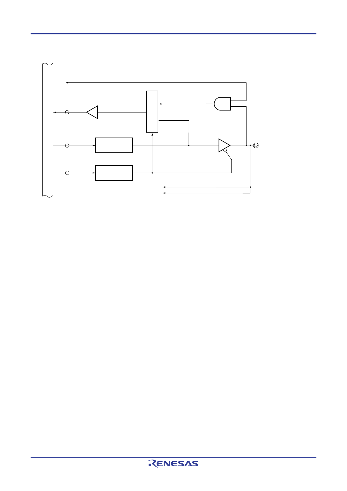
78K0/Fx2-L CHAPTER 4 PORT FUNCTIONS
Figure 4-8. Block Diagram of P26
RD
Selector
PORT
WR
Internal bus
WR
PM
P2
Output latch
(P26)
PM2
PM26
P26/ANI6/CMPCOM
A/D converter
Comparator common (-) input
R01UH0068EJ0203 Rev.2.03 93
Jun 29, 2012
Page 94

78K0/Fx2-L CHAPTER 4 PORT FUNCTIONS
4.2.3 Port 3
78K0/FY2-L (16 Pins) 78K0/FA2-L (20 Pins) 78K0/FB2-L (30 Pins)
P30/TOH1/TI51/INTP1 P30/TOH1/TI51/INTP1 P30/TOH1/TI51/INTP1
−
−
− −
− −
− −
− −
− −
Port 3 is an I/O port with an output latch. Port 3 can be set to the input mode or output mode in 1-bit units using port
mode register 3 (PM3). When the P30 to P37 pins are used as an input port, us e of an on-chip pull-up resistor can be
specified in 1-bit units by pull-up resistor option register 3 (PU3).
This port can also be used for external interrupt request input, timer I/O, clock I/O and data I/O for serial interface, and
clock input and data I/O for flash memory programmer/on-chip debugger.
Reset signal generation sets port 3 to input mode.
Figures 4-9 to 4-16 show block diagrams of port 3.
Caution To use P35/SCK11 and P37/SO11 of 78K0/FB2-L as general-purpose ports, set serial operation mode
register 11 (CSIM11) and serial clock selection register 11 (CSIC11) to the default status (00H).
Remark For how to connect a flash memory programmer using TOOLC1/P31, TOOLD1/P32, refer to CH APTER 24
FLASH MEMORY. For how to connect TOOLC1/P31, TOOLD1/P32 and an on-chip debug emulator, refer
to CHAPTER 25 ON-CHIP DEBUG FUNCTION.
P31/TOX10/INTP2/TOOLC1 P31/TOX00/INTP2/TOOLC1
P32/TOX11/INTP3/TOOLD1 P32/TOX01/INTP3/TOOLD1
P33/TOX10
P34/TOX11/INTP4
P35/SCK11
P36/SI11
P37/SO11
R01UH0068EJ0203 Rev.2.03 94
Jun 29, 2012
Page 95
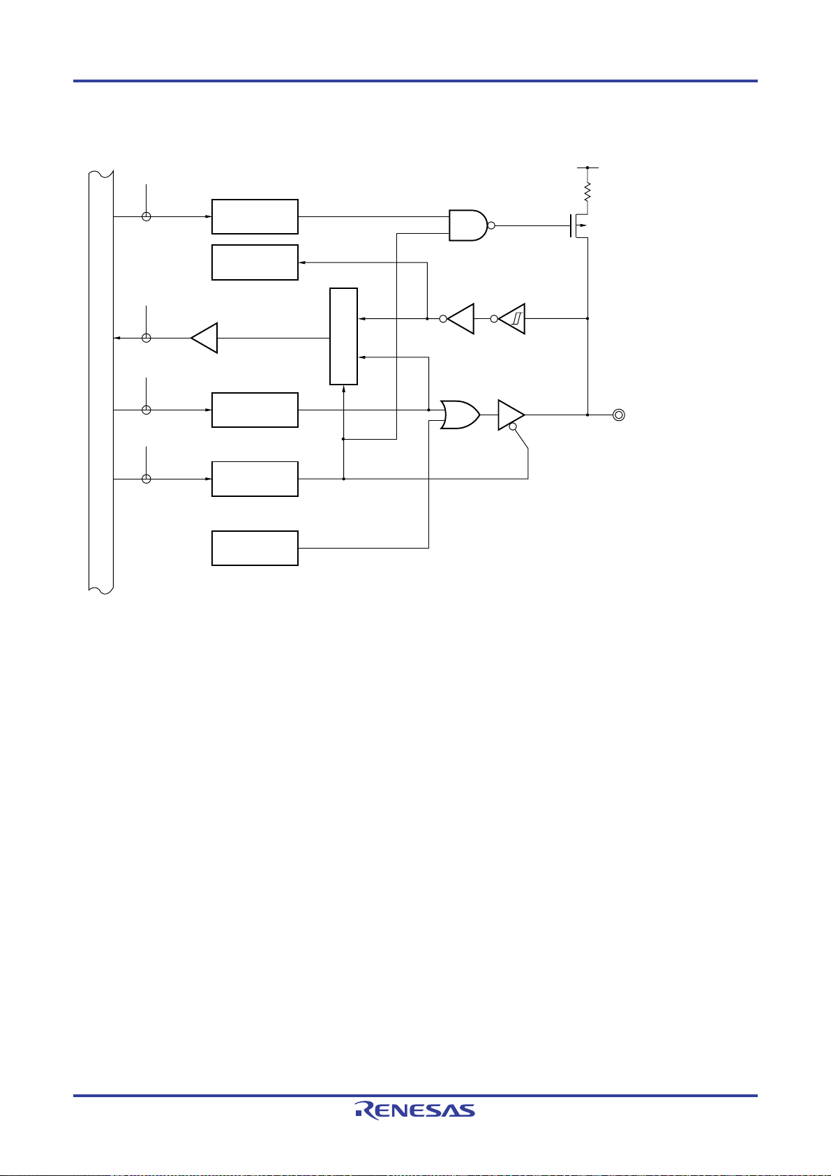
78K0/Fx2-L CHAPTER 4 PORT FUNCTIONS
Figure 4-9. Block Diagram of P30
PU
WR
PU3
V
DD
PU30
Alternate
function
RD
WR
PORT
Internal bus
WR
PM
P3
Output latch
(P30)
PM3
PM30
Alternate
function
P3: Port register 3
PU3: Pull-up resistor option register 3
PM3: Port mode register 3
RD: Read signal
WR××: Write signal
P-ch
Selector
P30/TOH1/TI51/INTP1
R01UH0068EJ0203 Rev.2.03 95
Jun 29, 2012
Page 96

78K0/Fx2-L CHAPTER 4 PORT FUNCTIONS
Figure 4-10. Block Diagram of P31
PU
WR
PU3
V
DD
PU31
Alternate
function
RD
WR
PORT
Internal bus
WR
PM
P3
Output latch
(P31)
PM3
PM31
Alternate
function
P3: Port register 3
PU3: Pull-up resistor option register 3
PM3: Port mode register 3
RD: Read signal
WR××: Write signal
P-ch
Selector
P31/TOX00/INTP2/TOOLC1
R01UH0068EJ0203 Rev.2.03 96
Jun 29, 2012
Page 97

78K0/Fx2-L CHAPTER 4 PORT FUNCTIONS
Figure 4-11. Block Diagram of P32
PU
WR
PU3
V
DD
PU32
Alternate
function
RD
WR
PORT
Internal bus
WR
PM
P3
Output latch
(P32)
PM3
PM32
Alternate
function
P3: Port register 3
PU3: Pull-up resistor option register 3
PM3: Port mode register 3
RD: Read signal
WR××: Write signal
P-ch
Selector
P32/TOX01/INTP3/TOOLD1
R01UH0068EJ0203 Rev.2.03 97
Jun 29, 2012
Page 98

78K0/Fx2-L CHAPTER 4 PORT FUNCTIONS
Figure 4-12. Block Diagram of P33
PU
WR
PU3
V
DD
RD
WR
PORT
Internal bus
WR
PM
PU33
Selector
P3
Output latch
(P33)
PM3
PM33
Alternate
function
P-ch
P33/TOX10
P3: Port register 3
PU3: Pull-up resistor option register 3
PM3: Port mode register 3
RD: Read signal
WR××: Write signal
R01UH0068EJ0203 Rev.2.03 98
Jun 29, 2012
Page 99

78K0/Fx2-L CHAPTER 4 PORT FUNCTIONS
Figure 4-13. Block Diagram of P34
WR
PU
PU3
V
DD
PU34
Alternate
function
RD
WR
PORT
Internal bus
WR
PM
P3
Output latch
(P34)
PM3
PM34
Alternate
function
P3: Port register 3
PU3: Pull-up resistor option register 3
PM3: Port mode register 3
RD: Read signal
WR××: Write signal
P-ch
Selector
P34/TOX11/INTP4
R01UH0068EJ0203 Rev.2.03 99
Jun 29, 2012
Page 100

78K0/Fx2-L CHAPTER 4 PORT FUNCTIONS
Figure 4-14. Block Diagram of P35
PU
WR
PU3
V
DD
RD
WR
PORT
Internal bus
WR
PU35
Alternate
function
Selector
P3
Output latch
(P35)
PM
PM3
PM35
Alternate
function
P-ch
P35/SCK11
P3: Port register 3
PU3: Pull-up resistor option register 3
PM3: Port mode register 3
RD: Read signal
WR××: Write signal
R01UH0068EJ0203 Rev.2.03 100
Jun 29, 2012
 Loading...