

Page 1

To our customers,
Old Company Name in Catalogs and Other Documents
On April 1st, 2010, NEC Electronics Corporation merged with Renesas Technology
Corporation, and Renesas Electronics Corporation took over all the business of both
companies. Therefore, although the old company name remains in this document, it is a valid
Renesas Electronics document. We appreciate your understanding.
Renesas Electronics website: http://www.renesas.com
April 1
Renesas Electronics Corporation
Issued by: Renesas Electronics Corporation (http://www.renesas.com)
st
, 2010
Send any inquiries to http://www.renesas.com/inquiry
.
Page 2

Notice
1. All information included in this document is current as of the date this document is issued. Such information, however, is
subject to change without any prior notice. Before purchasing or using any Renesas Electronics products listed herein, please
confirm the latest product information with a Renesas Electronics sales office. Also, please pay regular and careful attention to
additional and different information to be disclosed by Renesas Electronics such as that disclosed through our website.
2. Renesas Electronics does not assume any liability for infringement of patents, copyrights, or other intellectual property rights
of third parties by or arising from the use of Renesas Electronics products or technical information described in this document.
No license, express, implied or otherwise, is granted hereby under any patents, copyrights or other intellectual property rights
of Renesas Electronics or others.
3. You should not alter, modify, copy, or otherwise misappropriate any Renesas Electronics product, whether in whole or in part.
4. Descriptions of circuits, software and other related information in this document are provided only to illustrate the operation of
semiconductor products and application examples. You are fully responsible for the incorporation of these circuits, software,
and information in the design of your equipment. Renesas Electronics assumes no responsibility for any losses incurred by
you or third parties arising from the use of these circuits, software, or information.
5. When exporting the products or technology described in this document, you should comply with the applicable export control
laws and regulations and follow the procedures required by such laws and regulations. You should not use Renesas
Electronics products or the technology described in this document for any purpose relating to military applications or use by
the military, including but not limited to the development of weapons of mass destruction. Renesas Electronics products and
technology may not be used for or incorporated into any products or systems whose manufacture, use, or sale is prohibited
under any applicable domestic or foreign laws or regulations.
6. Renesas Electronics has used reasonable care in preparing the information included in this document, but Renesas Electronics
does not warrant that such informatio n is error free. Renesas Electronics assumes no liability whatsoever for any damages
incurred by you resulting from errors in or omissions from the information included herein.
7. Renesas Electronics products are classified according to the following three quality grades: “Standard”, “High Quality”, and
“Specific”. The recommended applications for each Renesas Electronics product depends on the product’s quality grade, as
indicated below. You must check the quality grade of each Renesas Electronics product before using it in a particular
application. You may not use any Renesas Electronics product for any application categorized as “Specific” without the prior
written consent of Renesas Electronics. Further, you may not use any Renesas Electronics product for any application for
which it is not intended without the prior written consent of Renesas Electronics. Renesas Electronics shall not be in any way
liable for any damages or losses incurred by you or third parties arising from the use of any Renesas Electronics product for an
application categorized as “Specific” or for which the product is not intended where you have failed to obtain the prior written
consent of Renesas Electronics. The quality grade of each Renesas Electronics product is “Standard” unless otherwise
expressly specified in a Ren esas E lectronics data sheets or dat a books, etc.
“Standard”: Computers; office equipment; communications equipment; test and measurement equipment; audio and visual
equipment; home electron ic appliances; machine tools; personal electronic equipment; and industrial robots.
“High Quality”: Transportation equipment (automobiles, trains, ships, etc.); traffic control systems; anti-disaster systems; anti-
crime systems; safety equipment; and medical equipment not specifically designed for life support.
“Specific”: Aircraft; aerospace equipment; submersible repeaters; nuclear reactor control systems; medical equipment or
systems for life support (e.g. artificial life support devices or systems), surgical implantations, or healthcare
intervention (e.g. excision, etc.), and any other appl i cations or purposes that pose a d irect threat to human life.
8. You should use the Renesas Electronics products described in this document within the range specified by Renesas Electronics,
especially with respect to the maximum rating, operating supply voltage range, movement power voltage range, heat radiation
characteristics, installation and other product characteristics. Renesas Electronics shall have no liability for malfunctions or
damages arising out of the use of Renesas Electronics products beyond such specified ranges.
9. Although Renesas Electronics endeavors to improve the quality and reliability of its products, semiconductor products have
specific characteristics such as t he occu rrence o f failure at a certai n rate an d malfunct io ns under cert ain u se con dition s. Further,
Renesas Electronics prod ucts are not subject to radiation resistance design. Please be sure to implement safety measures to
guard them against the possibility of physical injury, and injury or damage caused by fire in the event of the failure of a
Renesas Electronics product, such as safety design for hardware and software including but not limited to redundancy, fire
control and malfunction prevention, appropriate treatment for aging degradation or any other appropriate measures. Because
the evaluation of microcomputer software alone is very difficult, please evaluate the safety of the final products or system
manufactured by you.
10. Please contact a Renesas Electronics sales office for details as to environmental matters such as the environmental
compatibility of each Renesas Electronics product. Please use Renesas Electronics products in compliance with all applicable
laws and regulations that regulate the inclusion or use of controlled substances, including without limitation, the EU RoHS
Directive. Renesas Electronics assumes no liability for damages or losses occurring as a result of your noncompliance with
applicable laws and regulations.
11. This document may not be reproduced or duplicated, in any form, in whole or in part, without prior written consent of Renesas
Electronics.
12. Please contact a Renesas Electronics sales office if you have any questions regarding the information contained in this
document or Renesas Electronics products, or if you have any other inquiries.
(Note 1) “Renesas Electronics” as used in this document means Renesas Electronics Corporation an d also includes its majority-
owned subsidiaries.
(Note 2) “Renesas Electronics product(s)” means any product developed or manufactured by or for Renesas Electronics.
Page 3
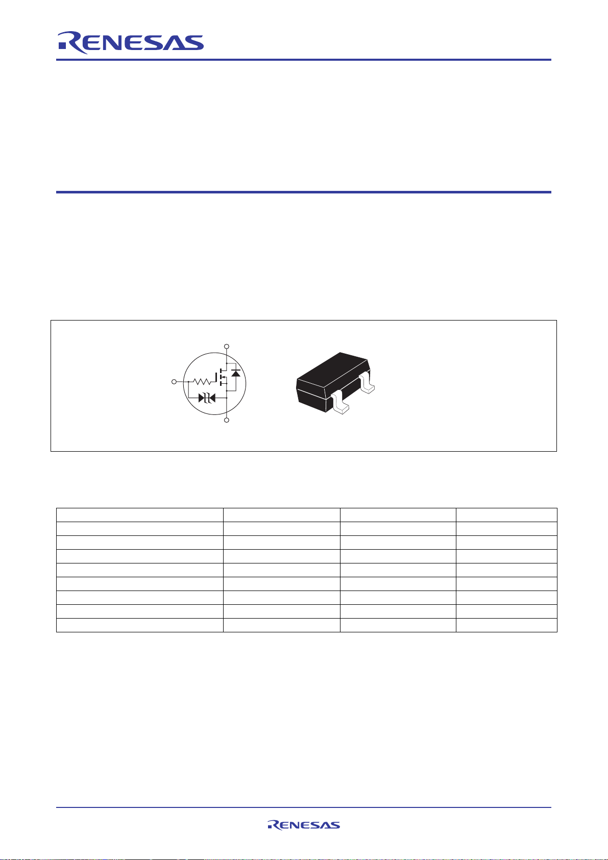
2SK3000
Silicon N Channel MOS FET
Low Frequency Power Switching
Features
• Low on-resistance
R
= 0.16 Ω typ. (V
DS(on)
• 4 V gate drive devices.
• Small package (MPAK)
• Expansive drain to source surge power capability
Outline
= 10 V, ID = 450 mA)
GS
REJ03G0379-0300Z
(Previous ADE-208-585A (Z))
Rev.3.00
Jun.15.2004
MPAK
G
2
D
3
3
1
1
S
2
1. Source
2. Gate
3. Drain
Note: Marking is “ZY–”.
Absolute Maximum Ratings
(Ta = 25°C)
Item Symbol Ratings Unit
Drain to source voltage V
Gate to source voltage V
Drain current I
Drain peak current I
Reverse drain current I
Channel dissipation Pch
Channel temperature Tch 150 °C
Storage temperature Tstg –55 to +150 °C
Notes: 1. PW ≤ 10 µs, duty cycle ≤ 1 %
2. When using the glass epoxy board (10 mm x 10 mm x 1 mm
D(pulse)
DSS
GSS
D
DR
Note2
Note1
t
)
40 V
±10 V
1.0 A
4.0 A
1.0 A
400 mW
Rev.3.00, Jun.16.2004, page 1 of 6
Page 4

2SK3000
Electrical Characteristics
Item Symbol Min Typ Max Unit Test Conditions
Drain to source breakdown voltage V
Drain to source voltage V
Gate to source breakdown voltage V
Zero gate voltage drain current I
Gate to source leak current I
Gate to source cutoff voltage V
(BR)DSS
DS(SUS)
(BR)GSS
DSS
GSS
GS(off)
Forward transfer admittance |yfs|0.51.2— SI
Static drain to source on state
resistance
R
R
DS(on)
DS(on)
Input capacitance Ciss — 14.0 — pF
Output capacitance Coss — 68 — pF
Reverse transfer capacitance Crss — 3.0 — pF
Turn-on delay time t
Rise time t
Turn-off delay time t
Fall time t
d(on)
r
d(off)
f
Notes: 3. Pulse test
40 — 60 V ID = 100 µA, VGS = 0
40 — — V L = 100 µH, ID = 3 A
±10 — — V IG = ±100 µA, VDS = 0
——1.0µAVDS = 40 V, VGS = 0
——±5 µAVGS = ±6.5V, VDS = 0
1.1 — 2.1 V ID = 10 µA, VDS = 5 V
= 450 mA, VDS = 10 V
D
— 0.24 0.5 Ω ID = 450 mA, VGS = 4V
— 0.16 0.3 Ω ID = 450 mA, VGS = 10 V
VDS = 10 V
= 0
V
GS
f = 1 MHz
—0.12— µs
—0.6—µs
VGS = 4 V, ID = 450 mA
= 22 Ω
R
L
—1.7—µs
—1.4—µs
(Ta = 25°C)
Note3
Note3
Note3
Rev.3.00, Jun.16.2004, page 2 of 6
Page 5

2SK3000
Main Characteristics
Power vs. Temperature Derating
0.8
0.6
0.4
0.2
Channel Dissipation Pch (W)
0
50 100 150 200
Ambient Temperature Ta (°C)
5.0
4.0
D
Typical Output Characteristics
10 V
6 V
5 V
4 V
4.5 V
3.0
3.5 V
2.0
Pulse Test
Maximum Safe Operation Area
5
0.1 ms
2
1
D
0.5
0.2
0.1
0.05
Operation in
Drain Current I (A)
this area is
0.02
limited by R
0.01
Ta = 25°C
0.05
0.2 0.5 2 5 20
PW = 100 ms (1 shot)
DC Operation
DS(on)
11050
1 ms
10 ms
Note4
Drain to Source Voltage V (V)
Note4 : When using the glass epoxy board
(10mm x 10mm x 1mm )
Typical Transfer Characteristics
10
1
D
100m
125°C
25°C
Tc = –25°C
10m
50 µs
100 200
DS
t
Drain Current I (A)
1.0
V = 2.5 V
0
246810
3 V
GS
Drain to Source Voltage V (V)
Drain to Source Saturation Voltage vs.
Gate to Source Voltage
1.0
0.8
DS(on)
V (V)
0.6
0.4
0.2
Drain to Source Saturation Voltage
0
48
12
Drain Current I (A)
1m
100µ
0
DS
Gate to Source Voltage V
Static Drain to Source on State Resistance
Pulse Test
10
Pulse Test
3
1
DS(on)
R ( )Ω
0.3
I = 2 A
D
1 A
0.45 A
16 20 0.01 10.1
0.1
0.03
Drain to Source On State Resistance
0.01
0.03 0.3 3
V = 5 V
DS
Pulse Test
12345
(V)
GS
vs. Drain Current
V = 4 V
GS
10 V
10
Rev.3.00, Jun.16.2004, page 3 of 6
Page 6

2SK3000
Static Drain to Source on State Resistance
0.5
0.4
DS(on)
R (Ω)
0.3
V
0.2
0.1
0
–40 0 40 80 120 160
Static Drain to Source on State Resistance
vs. Temperature
= 4 V
GS
10 V
ID = 0.45 A
0.45 A
Pulse Test
Case Temperature Tc (°C)
Typical Capacitance vs.
Drain to Source Voltage
500
200
100
V = 0
f = 1 MHz
Coss
GS
50
20
Ciss
10
Capacitance C (pF)
5
Crss
2
1
048121620
Drain to Source Voltage V (V)
DS
Forward Transfer Admittance vs.
Drain Current
10
fs
5
Tc = –25°C
2
1
25°C
75°C
0.5
0.2
Forward Transfer Admittance |y | (S)
0.1
V = 10 V
DS
Pulse Test
0.1 0.2 0.5 1 2 10
Drain Current I (A)
D
Switching Characteristics
5000
t
2000
1000
d(off)
t
f
t
r
500
200
Switching Time t (ns)
100
50
0.05
t
d(on)
V = 4 V, V = 10 V
GS
DD
PW = 5 µs, duty < 1 %
0.50.20.1
1
Drain Current I (A)
D
5
52
Drain to Source DiodeReverse Surge
Destruction Characteristics
500
200
100
50
20
Applied Power Ps (W)
10
5
0.05 1
0.50.20.1
Surge Pulse Width PW (mS)
Ta = 25°C
1 shot
10525020
Reverse Drain Current vs.
Source to Drain Voltage
5
10 V
5 V
V = 0
4
DR
3
2
1
Reverse Drain Current I (A)
0
0.4 0.8 1.2 1.6 2.0
Source to Drain Voltage V (V)
GS
Pulse Test
SD
Rev.3.00, Jun.16.2004, page 4 of 6
Page 7
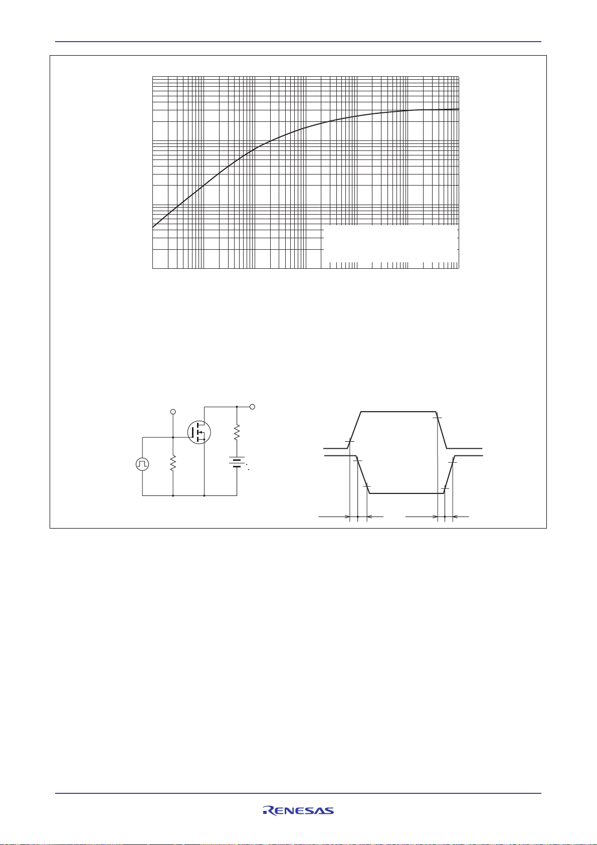
2SK3000
Transient Thermal Resistance
1000
300
100
θ j–a (°C/W)
30
10
Thermal Resistance
3
1
1 m
Switching Time Test Circuit Switching Time Waveforms
Vin Monitor
Vin
50Ω
4 V
Condition :
Ta = 25°C
When using the glass epoxy board
(10mm x 10mm x 1mm )
t
10 m 100 m 1 10 100 1000
Pulse Width PW (S)
Vout
D.U.T.
R
L
V
DD
= 10 V
Monitor
Vin
Vout
td(on)
10%
10%
90%
tr
td(off)
90%
10%
90%
t
f
Rev.3.00, Jun.16.2004, page 5 of 6
Page 8

2SK3000
Package Dimensions
As of January, 2003
Unit: mm
0.4
+ 0.10
– 0.05
0.95
1.9 ± 0.2
0.95
0.65
+ 0.2
– 0.6
2.8
1.5 ± 0.15
0.65
+ 0.10
0.16
– 0.06
0 – 0.1
2.95 ± 0.2
0.3
+ 0.2
– 0.1
1.1
Package Code
JEDEC
JEITA
(reference value)
Mass
MPAK(T)
—
Conforms
0.011 g
Ordering Information
Part Name Quantity Shipping Container
2SK3000 3000 pcs φ178 mm Reel Taping (T L)
Note: For some grades, production may be terminated. Please contact the Renesas sales office to check the state of
production before ordering the product.
Rev.3.00, Jun.16.2004, page 6 of 6
Page 9

Sales Strategic Planning Div. Nippon Bldg., 2-6-2, Ohte-machi, Chiyoda-ku, Tokyo 100-0004, Japan
m
C
.0
Keep safety first in your circuit designs!
1. Renesas Technology Corp. puts the maximum effort into making semiconductor products better and more reliable, but there is always the possibility that trouble
may occur with them. Trouble with semiconductors may lead to personal injury, fire or property damage.
Remember to give due consideration to safety when making your circuit designs, with appropriate measures such as (i) placement of substitutive, auxiliary
circuits, (ii) use of nonflammable material or (iii) prevention against any malfunction or mishap.
Notes regarding these materials
1. These materials are intended as a reference to assist our customers in the selection of the Renesas Technology Corp. product best suited to the customer's
application; they do not convey any license under any intellectual property rights, or any other rights, belonging to Renesas Technology Corp. or a third party.
2. Renesas Technology Corp. assumes no responsibility for any damage, or infringement of any third-party's rights, originating in the use of any product data,
diagrams, charts, programs, algorithms, or circuit application examples contained in these materials.
3. All information contained in these materials, including product data, diagrams, charts, programs and algorithms represents information on products at the time of
publication of these materials, and are subject to change by Renesas Technology Corp. without notice due to product improvements or other reasons. It is
therefore recommended that customers contact Renesas Technology Corp. or an authorized Renesas Technology Corp. product distributor for the latest product
information before purchasing a product listed herein.
The information described here may contain technical inaccuracies or typographical errors.
Renesas Technology Corp. assumes no responsibility for any damage, liability, or other loss rising from these inaccuracies or errors.
Please also pay attention to information published by Renesas Technology Corp. by various means, including the Renesas Technology Corp. Semiconductor
home page (http://www.renesas.com).
4. When using any or all of the information contained in these materials, including product data, diagrams, charts, programs, and algorithms, please be sure to
evaluate all information as a total system before making a final decision on the applicability of the information and products. Renesas Technology Corp. assumes
no responsibility for any damage, liability or other loss resulting from the information contained herein.
5. Renesas Technology Corp. semiconductors are not designed or manufactured for use in a device or system that is used under circumstances in which human life
is potentially at stake. Please contact Renesas Technology Corp. or an authorized Renesas Technology Corp. product distributor when considering the use of a
product contained herein for any specific purposes, such as apparatus or systems for transportation, vehicular, medical, aerospace, nuclear, or undersea repeater
use.
6. The prior written approval of Renesas Technology Corp. is necessary to reprint or reproduce in whole or in part these materials.
7. If these products or technologies are subject to the Japanese export control restrictions, they must be exported under a license from the Japanese government and
cannot be imported into a country other than the approved destination.
Any diversion or reexport contrary to the export control laws and regulations of Japan and/or the country of destination is prohibited.
8. Please contact Renesas Technology Corp. for further details on these materials or the products contained therein.
RENESAS SALES OFFICES
Renesas Technology America, Inc.
450 Holger Way, San Jose, CA 95134-1368, U.S.A
Tel: <1> (408) 382-7500 Fax: <1> (408) 382-7501
Renesas Technology Europe Limited.
Dukes Meadow, Millboard Road, Bourne End, Buckinghamshire, SL8 5FH, United Kingdom
Tel: <44> (1628) 585 100, Fax: <44> (1628) 585 900
Renesas Technology Europe GmbH
Dornacher Str. 3, D-85622 Feldkirchen, Germany
Tel: <49> (89) 380 70 0, Fax: <49> (89) 929 30 11
Renesas Technology Hong Kong Ltd.
7/F., North Tower, World Finance Centre, Harbour City, Canton Road, Hong Kong
Tel: <852> 2265-6688, Fax: <852> 2375-6836
Renesas Technology Taiwan Co., Ltd.
FL 10, #99, Fu-Hsing N. Rd., Taipei, Taiwan
Tel: <886> (2) 2715-2888, Fax: <886> (2) 2713-2999
Renesas Technology (Shanghai) Co., Ltd.
26/F., Ruijin Building, No.205 Maoming Road (S), Shanghai 200020, China
Tel: <86> (21) 6472-1001, Fax: <86> (21) 6415-2952
Renesas Technology Singapore Pte. Ltd.
1, Harbour Front Avenue, #06-10, Keppel Bay Tower, Singapore 098632
Tel: <65> 6213-0200, Fax: <65> 6278-8001
http://www.renesas.co
© 2004. Renesas Technology Corp., All rights reserved. Printed in Japan.
olophon .1
 Loading...