

realtek rtl8201bl Datasheet

REALTEK SINGLE CHIP
SINGLE PORT 10/100M
FAST ETHERNET PHYCEIVER
RTL8201BL
RTL8201BL
1. Features...........................................................................2
2. General Description.......................................................2
3. Block Diagram................................................................3
4. Pin Assignments.............................................................4
5. Pin Description...............................................................5
5.1 100 Mbps MII & PCS Interface ................................ 5
5.2 SNI (Serial Network Interface): 10Mbps only .......... 5
5.3 Clock Interface.......................................................... 6
5.4 100Mbps Network Interface...................................... 6
5.5 Device Configuration Interface................................. 6
5.6 LED Interface/PHY Address Config......................... 7
5.7 Reset and other pins .................................................. 7
5.8 Power and Ground pins............................................. 7
6. Register Descriptions.....................................................8
6.1 Register 0 Basic Mode Control Register................... 8
6.2 Register 1 Basic Mode Status Register .....................9
6.3. Register 2 PHY Identifier Register 1 ....................... 9
6.4. Register 3 PHY Identifier Register 2 ....................... 9
6.5. Register 4 Auto-negotiation Advertisement
Register(ANAR) ...........................................................10
6.6 Register 5 Auto-Negotiation Link Partner Ability
Register(ANLPAR) ....................................................... 10
6.7 Register 6 Auto-negotiation Expansion
Register(ANER)............................................................ 11
6.8 Register 16 Nway Setup Register(NSR) ................. 11
6.9 Register 17 Loopback, Bypass, Receiver Error Mask
Register(LBREMR) ......................................................12
6.10 Register 18 RX_ER Counter(REC)....................... 12
6 .1 1 Register 19 10Mbps Network Interface Configuration Register.. . 1 2
6.12 Register 20 PHY 1_1 Register .............................. 13
6.13 Register 21 PHY 1_2 Register .............................. 13
6.14 Register 22 PHY 2 Register .................................. 13
6.15 Register 23 Twister_1 Register .............................13
6.16 Register 24 Twister_2 Register .............................13
6.17 Register 25 Test Register....................................... 13
7. Functional Description ................................................ 14
7.1 MII and Management Interface............................... 14
7.1.1 Data Transition................................................ 14
7.1.2 Serial Management.......................................... 14
7.2 Auto-negotiation and Parallel Detection................. 15
7.3 Flow control support............................................... 16
7.4 Hardware Configuration and Auto-negotiation................. 16
7.5 LED and PHY Address Configuration.................... 17
7.6 Serial Network Interface......................................... 17
7 .7 Power Down, Link Down, Power Saving, and Isolation Modes .. . 1 8
7.8 Media Interface....................................................... 18
7.8.1 100Base TX..................................................... 18
7.8.2 100Base-FX Fiber Mode Operation ................ 18
7.8.3 10Base Tx/Rx.................................................. 19
7.9 Repeater Mode Operation....................................... 19
7.10 Reset, and Transmit Bias(RTSET)........................ 19
7.11 3.3V power supply and voltage conversion circuit 19
7.12 Far End Fault Indication (FEFI)............................ 20
8. Electrical Characteristics............................................ 21
8.1 D.C. Characteristics ................................................ 21
8.1.1. Absolute Maximum Ratings........................... 21
8.1.2. Operating Conditions ..................................... 21
8.1.3. Power Dissipation........................................... 21
8.1.4 Supply Voltage: Vcc ........................................ 21
8.2 A.C. Characteristics ................................................ 22
8.2.1 MII Timing of Transmission Cycle ................. 22
8.2.2 MII Timing of Reception Cycle ...................... 23
8.2.3 SNI Timing of Transmission Cycle................. 24
8.2.4 SNI Timing of Reception Cycle ...................... 25
8.2.5 MDC/MDIO timing......................................... 26
8.2.6 Transmission Without Collision ...................... 26
8.2.7 Reception Without Error ................................. 26
8.3 Crystal and Transformer Specifications.................. 27
8.3.1 Crystal Specifications...................................... 27
8.3.2 Transformer Specifications.............................. 27
9. Mechanical Dimensions...............................................28
10. Revision History......................................................... 29
2002-03-29 Rev.1.2
1

RTL8201BL
1. Features
The Realtek RTL8201BL is a Fast Ethernet Phyceiver with selectable MII or SNI interface to the MAC chip. It provides the
following features:
Supports MII/7-wire SNI (Serial Network
Interface) interface
Supports 10/100Mbps operation
Supports half/full duplex operation
Support of twisted pair or Fiber mode output
IEEE 802.3/802.3u compliant
Supports IEEE 802.3u clause 28 auto negotiation
Supports power down mode
Supports operation under Link Down Power
Saving mode
Supports Base Line Winder (BLW) compensation
Supports repeater mode
Speed/duplex/auto negotiation adjustable
3.3V operation with 5V IO signal tolerance
Low operation power consumption and only need
single supply 3.3V
Adaptive Equalization
25MHz crystal/oscillator as clock source
Multiple network status LED support
Flow control ability support to co-work with
MAC (by MDC/MDIO)
48 pin LQFP package
2. General Description
The RTL8201BL is a single-port Phyceiver with an MII (Media Independent Interface)/SNI(Serial Network Interface). It
implements all 10/100M Ethernet Physical-layer functions including the Physical Coding Sublayer (PCS), Physical Medium
Attachment (PMA), Twisted Pair Physical Medium Dependent Sublayer (TP-PMD), 10Base-Tx Encoder/Decoder and Twisted
Pair Media Access Unit (TPMAU). A PECL interface is supported to connect with an external 100Base-FX fiber optical
transceiver. The chip is fabricated with an advanced CMOS process to meet low voltage and low power requirements.
The RTL8201BL can be used as a Network Interface Adapter, MAU, CNR, ACR, Ethernet Hub, Ethernet Switch. Additionally,
it can be used in any embedded system with an Ethernet MAC that needs a twisted pair physical connection or fiber PECL
interface to external 100Base-FX optical transceiver module.
2002-03-29 Rev.1.2
2
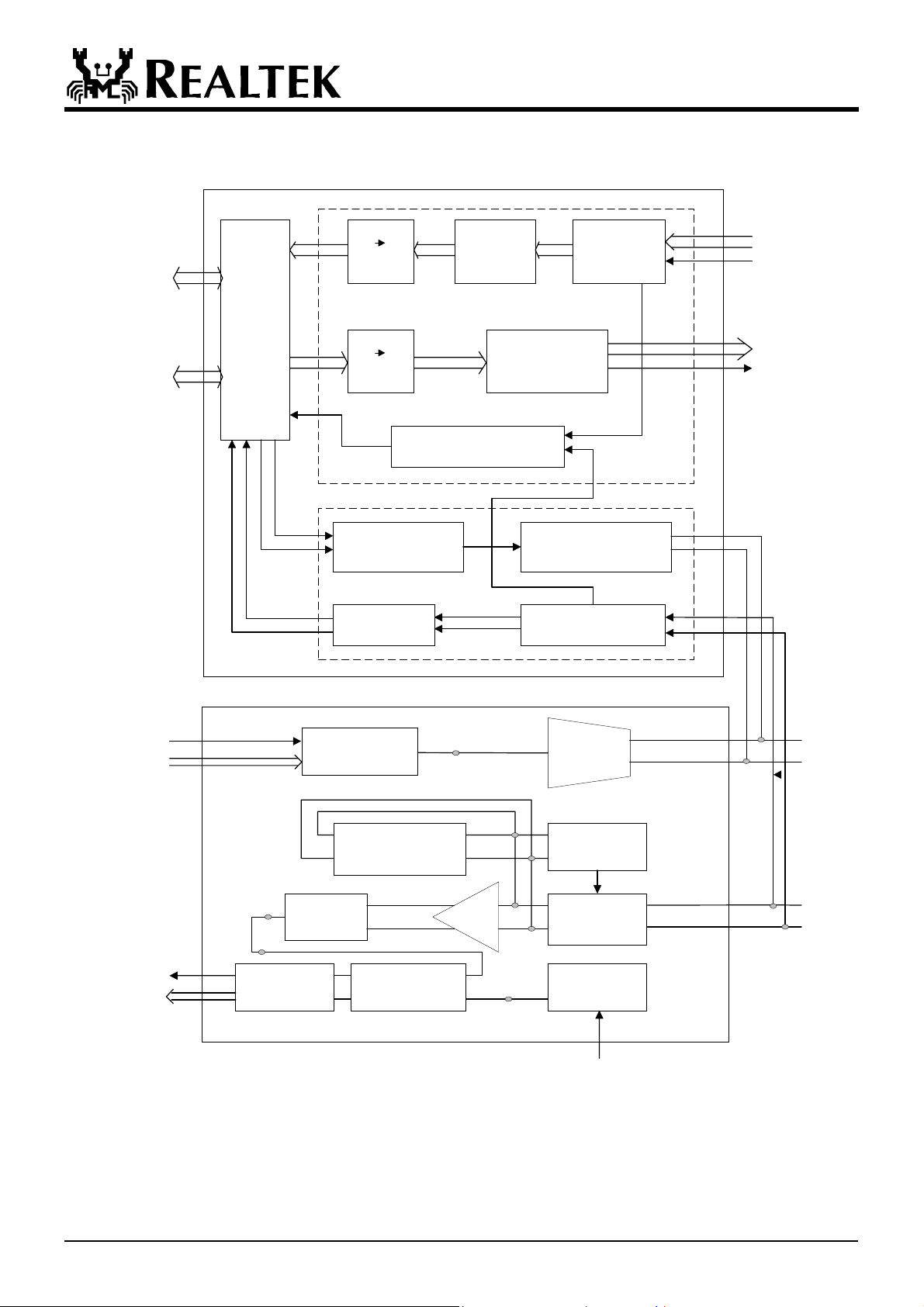
3. Block Diagram
100M
RTL8201BL
MII
Interface
SNI
Interface
10/100
half/full
Switch
Logic
TXC10
TXD10
RXC10
RXD10
5B 4B
Decoder
4B 5B
Encoder
10/100M Auto-negotiation
Data
Alignment
Control Logic
Descrambler
Scrambler
10M
Manchester coded
waveform
Data Recovery Receive low pass filter
10M Output waveform
shaping
RXD
RXC 25M
TXD
TXC 25M
Link pulse
TXC 25M
TXD
RXC 25M
RXD
Serial to
Parrallel
Parrallel
MLT-3
to NRZI
to Serial
Correction
ck
data
Variable Current
Baseline
wander
Slave
PLL
TD+
3 Level
Comparator
Control
Voltage
3 Level
Driver
Peak
Detect
Adaptive
Equalizer
Master
PPL
25M
TXO+
TXO -
RXIN+
RXIN-
2002-03-29 Rev.1.2
3
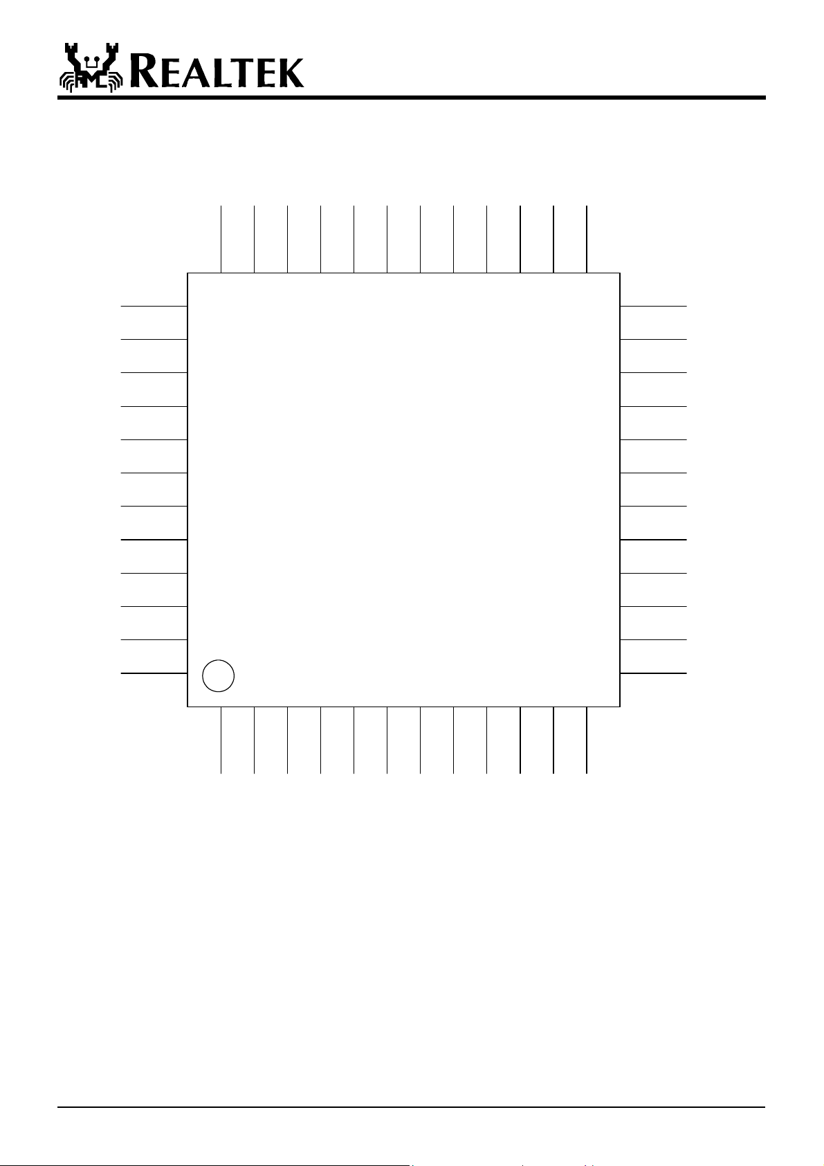
4. Pin Assignments
35. AGND
34. TPTX+
36. AVDD33
37. ANE
RTL8201BL
25. MDC
33. TPTX-
31. TPRX+
32. PWFBOUT
30. TPRX-
29. AGND
28. RTSET
26. MDIO
27. NC
24. RXER
/FX E N
38. DUPLEX
39. SPEED
40. RPTR
41. LDPS
42. RESETB
43. ISOLATE
44. MII/SNIB
/RT T3
45. DGND
46. X1
47. X2
48. DVDD33
RT L8201BL
23. CRS
22. RXDV
21. RXD0
20. RXD1
19. RXD2
18. RXD3
17. DGND
16. RXC
15. LED4/
PH YAD 4
14. DVDD33
13. LED3/
PH YAD 3
2. TXEN
3. TXD3
4. TXD2
1. COL
5. TXD1
2002-03-29 Rev.1.2
7. TXC
6. TXD0
9. LED0/
PHYAD0
10. LED1/
8. PWFBIN
PHYAD1
12. LED2/
11. DGND
PHYAD2
4

RTL8201BL
5. Pin Description
LI: Latched Input in power up or reset I/O: Bi-directional input and output
I: Input O: Output
P: Power
5.1 100 Mbps MII & PCS Interface
Symbol Type Pin No. Description
TXC O 7 Tr ansmit Cl ock : This pin provides a continuous clock as a timing reference
for TXD[3:0] and TXEN.
TXEN I 2 Transmit Enable: The input signal indicates the presence of a valid nibble
data on TXD[3:0].
TXD[3:0] I 3, 4, 5, 6 Tr a n sm i t D a t a : MAC will source TXD[0..3] synchronous with TXC when
TXEN is asserted.
RXC O 16 Receive Clock: This pin provides a continuous clock reference for RXDV
and RXD[0..3] signals. RXC is 25MHz in the 100Mbps mode and 2.5Mhz in
the 10Mbps mode.
COL O 1 Collision Detected: COL is asserted high when a collision is detected on the media.
CRS O 23 Carrier Sense: This pin’s signal is asserted high if the media is not in IDEL state.
RXDV O 22 Receive Data Valid: This pin’s signal is asserted high when received data is
present on the RXD[3:0] lines; the signal is deasserted at the end of the
packet. The signal is valid on the rising of the RXC.
RXD[3:0] O 18, 19, 20, 21 Receive Data: These are the four parallel receive data lines aligned on the
nibble boundaries driven synchronously to the RXC for reception by the
external physical unit (PHY).
RXER/
FXEN
MDC I 25 Management Data Clock: This pin provides a clock synchronous to MDIO,
MDIO I/O 26 Management Data Input/Output: This pin provides the bi-directional
O/LI
24 Receive error: if any 5B decode error occurs, such as invalid J/K, T/R,
invalid symbol, this pin will go high.
Fiber/UTP Enable: During power on reset, this pin status is latched to
determine at which media mode to operate:
1: Fiber mode
0: UTP mode
An internal weak pull low resistor, sets this to the default of UTP mode. It is
possible to use an external 5.1KΩ pull high resistor to enable fiber mode.
After power on, the pin operates as the Receive Error pin.
which may be asynchronous to the transmit TXC and receive RXC clocks.
The clock rate can be up to 2.5MHz.
signal used to transfer management information.
5.2 SNI (Serial Network Interface): 10Mbps only
Symbol Type Pin No. Description
COL O 1
RXD0 O 21
CRS O 23
RXC O 16 Receive Clock: Resolved from received data
TXD0 I 6
TXC O 7 Transmit Clock: Generate by PHY
TXEN I 2 Transmit Enable: For MAC to indicate transmit operation
2002-03-29 Rev.1.2
Collision Detect
Received Serial Data
Carrier Sense
Transmit Serial Data
5

RTL8201BL
5.3 Clock Interface
Symbol Type Pin No. Description
X2 O 47 25MHz Crystal Output: This pin provides the 25MHz crystal output. It
must be left open when X1 is driven with an external 25MHz oscillator.
X1 I 46 25MHz Crystal Input: This pin provides the 25MHz crystal input. If a
25MHz oscillator is used, connect X1 to the oscillator’s output. Refer to
section 8.3 to obtain clock source specifications.
5.4 100Mbps Network Interface
Symbol Type Pin No. Description
TPTX+
TPTX-
RTSET I 28 Transmit Bias Resistor Connection: This pin should be pulled to GND by
TPRX+
TPRX-
O
O
34
33
I
I
31
30
Transmit Output: Differential pair shared by 100Base-TX, 100Base-FX and
10Base-T modes. When configured as 100Base-TX, output is an MLT-3
encoded waveform. When configured as 100Base-FX, the output is
pseudo-ECL level.
a 5.9KΩ (1%) resistor to define driving current for transmit DAC. The
resistance value may be changed, depending on experimental results of the
RTL8201BL.
Receive Input: Differential pair shared by 100Base-TX, 100Base-FX, and
10Base-T modes.
5.5 Device Configuration Interface
Symbol Type Pin No. Description
ISOLATE I 43 Set high to isolate the RTL8201BL from the MAC. This will also isolate the
MDC/MDIO management interface. In this mode, the power consumption is
minimum. This pin can be directly connected to GND or VCC.
RPTR I 40 Set high to put the RTL8201BL into repeater mode. This pin can be directly
connected to GND or VCC.
SPEED LI 39 This pin is latched to input during a power on or reset condition. Set high to
put the RTL8201BL into 100Mbps operation. This pin can be directly connected
to GND or VCC.
DUPLEX LI 38 This pin is latched to input during a power on or reset condition. Set high to
enable full duplex. This pin can be directly connected to GND or VCC.
ANE LI 37 This pin is latched to input during a power on or reset condition. Set high to
enable Auto-negotiation mode, set low to force mode. This pin can be directly
connected to GND or VCC.
LDPS I 41 Set high to put the RTL8201BL into LDPS mode. This pin can be directly
connected to GND or VCC. Refer to Section 7.7 for more information.
MII/SNIB/
RTT3(test)
LI/O 44 This pin is latched to input during a power on or reset condition. Pull high to
set the RTL8201BL into MII mode operation. Set low for SNI mode. This pin
can be directly connected to GND or VCC. In test mode, this pin is an output pin and
redefined as RTT3
2002-03-29 Rev.1.2
6

RTL8201BL
5.6 LED Interface/PHY Address Config
These five pins are latched into the RTL8201BL during power up reset to configure PHY address [0:4] used for MII
management register interface. And then, in normal operation after initial reset, they are used as driving pins for status
indication LED. The driving polarity, active low or active high, is determined by each latched status of the PHY address [4:0]
during power-up reset. If latched status is High then it will be active low, and if latched status is Low then it will be active high.
Refer to Section 7.5 for more information.
Symbol Type Pin No. Description
PHYAD0/
LED0
PAD1/
LED1
PHYAD2/
LED2
PHYAD3/
LED3
PHYAD4/
LED4
LI/O 9
LI/O 10
LI/O 12
LI/O 13
LI/O 15
PHY Address [0]
Link LED:
PHY Address [1]
Full Duplex LED:
PHY Address [2]
Link 10/ACT LED:
when transmitting or receiving data.
PHY Address [3]
Link 100/ACT LED:
when transmitting or receiving data.
PHY Address [4]
Collision LED:
Active when linked.
Active when in Full Duplex operation.
Active when linked in 10Base-T mode, and blinking
Active when linked in 100Base-TX and blinking
Active when collisions occur.
5.7 Reset and other pins
Symbol Type Pin No. Description
RESETB I 42
PWFBOUT O 32
PWFBIN I 8
NC 27
RESETB:
must be asserted low for at least 10ms.
Power Feedback Output:
frequency compensation and a 0.1uF capacitor for noise de-coupling. Then
connect this pin through a ferrite bead to PWFBIN(pin8). The connection
method is figured in section 7.11.
Power Feedback Input:
Not connection
Set low to reset the chip. For a complete reset function, this pin
Be sure to connect a 22uF tantalum capacitor for
see the description of PWFBOUT.
5.8 Power and Ground pins
Symbol Type Pin No. Description
AVDD33 P 36
AGND P 29,35
DVDD33 P 14,48
DGND P 11,17,45
3.3V Analog power input:
well decoupled.
Analog Ground:
3.3V Digital Power input:
Digital Ground:
Should be connected to a larger GND plane
Should be connected to a larger GND plane.
3.3V power supply for analog circuit; should be
3.3V power supply for digital circuit.
2002-03-29 Rev.1.2
7

RTL8201BL
6. Register Descriptions
This section will describe definitions and usage for each of the registers available in the RTL8201BL.
6.1 Register 0 Basic Mode Control Register
Address Name Description/Usage Default/Attribute
0:<15> Reset This bit sets the status and control registers of the
PHY in a default state. This bit is self-clearing.
1 = software reset
0 = normal operation
0:<14> Loopback This bit enables loopback of transmit data nibbles
TXD<3:0> to the receive data path.
1 = enable loopback
0 = normal operation
0:<13> Spd_Set This bit sets the network speed.
1 = 100Mbps
0 = 10Mbps
When 100Base-FX mode is enabled, this bit=1 and is
read only.
0:<12> Auto
Negotiation
Enable
0:<11> Power Down This bit turns down the power of the PHY chip
0:<10> Reserved
0:<9> Restart Auto
Negotiation
0:<8> Duplex Mode This bit sets the duplex mode if auto negotiation is
0:<7:0> Reserved
This bit enables/disables the Nway auto-negotiation
function.
1 = enable auto-negotiation; bits 0:<13> and 0:<8>
will be ignored.
0 = disable auto-negotiation; bits 0:<13> and 0:<8>
will determine the link speed and the data transfer
mode, respectively.
When 100Base-FX mode is enabled, this bit=0 and is
read only.
including internal crystal oscillator circuit. The MDC,
MDIO is still alive for accessing the MAC.
1 = power down
0 = normal operation
This bits allows the Nway auto-negotiation function
to be reset.
1 = re-start auto-negotiation
0 = normal operation
disabled (bit 0:<12>=0)
1 = full duplex
0 = half duplex
After completing auto negotiation, this bit will reflect
the duplex status.(1: Full duplex, 0: Half duplex)
When 100Base-FX mode is enabled, this bit can be
set through the MDC/MDIO SMI interface or
DUPLEX pin.
0, RW
0, RW
1, RW
1, RW
0, RW
0, RW
1, RW
2002-03-29 Rev.1.2
8

RTL8201BL
6.2 Register 1 Basic Mode Status Register
Address Name Description/Usage Default/Attribute
1:<15> 100Base-T4 1 = enable 100Base-T4 support
0 = suppress 100Base-T4 support
1:<14> 100Base_TX_
FD
1:<13> 100BASE_TX_
HD
1:<12> 10Base_T_FD 1 = enable 10Base-T full duplex support
1:<11> 10_Base_T_HD 1 = enable 10Base-T half duplex support
1:<10:7> Reserved
1:<6> MF Preamble
Suppression
1:<5> Auto
Negotiation
Complete
1:<4> Remote Fault 1 = remote fault condition detected (cleared on read)
1:<3> Auto
Negotiation
1:<2> Link Status 1 = valid link established
1:<1> Jabber Detect 1 = jabber condition detected
1:<0> Extended
Capability
1 = enable 100Base-TX full duplex support
0 = suppress 100Base-TX full duplex support
1 = enable 100Base-TX half duplex support
0 = suppress 100Base-TX half duplex support
0 = suppress 10Base-T full duplex support
0 = suppress 10Base-T half duplex support
The RTL8201BL will accept management frames
with preamble suppressed. The RTL8201BL accepts
management frames without preamble. A Minimum
of 32 preamble bits are required for the first SMI
read/write transaction after reset. One idle bit is
required between any two management transactions
as per IEEE802.3u specifications
1 = auto-negotiation process completed
0 = auto-negotiation process not completed
0 = no remote fault condition detected
When in 100Base-FX mode, this bit means an
in-band signal Far-End-Fault is detected. Refer to
Section 7.11.
1 = Link had not been experienced fail state
0 = Link had been experienced fail state
0 = no valid link established
0 = no jabber condition detected
1 = extended register capability
0 = basic register capability only
0, RO
1, RO
1, RO
1, RO
1, RO
1, RO
0, RO
0, RO
1, RO
0, RO
0, RO
1, RO
6.3. Register 2 PHY Identifier Register 1
Address Name Description/Usage Default/Attribute
2:<15;0> PHYID1 PHY identifier ID for software recognize
RTL8201BL
0000, RO
6.4. Register 3 PHY Identifier Register 2
Address Name Description/Usage Default/Attribute
3:<15;0> PHYID2 PHY identifier ID for software recognize RTL8201 8201, RO
2002-03-29 Rev.1.2
9
 Loading...