

Page 1
A
R31
R31
1.5K
1.5K
VDD33
MDC PWFBOUT
MDIO AVDD33
TXD0
TXD1
TXD2
TXD3
C6
20PC620P
PWFBIN
GND
A
TXEN
TXCLK
RXDV
RXD0
RXD1
RXD2
RXD3
RXCLK
COL
CRS
RXER
LED0/PHYAD0
LED1/PHYAD1
LED2/PHYAD2
LED3/PHYAD3
LED4/PHYAD4
R18
R18
5.1K
5.1K
R20
R20
5.1K
5.1K
R21
R21
510
510
R22
R22
5.1K
5.1K
R24
R24
5.1K
5.1K
R26
R26
5.1K
5.1K
PWFBIN
VDD33
VDD33
R23
R23
510
510
R25
R25
510
510
Connect to MAC
4 4
which has MII
interface
Y1
Y1
C5
25.000Mhz
25.000Mhz
20PC520P
GNDGND
3 3
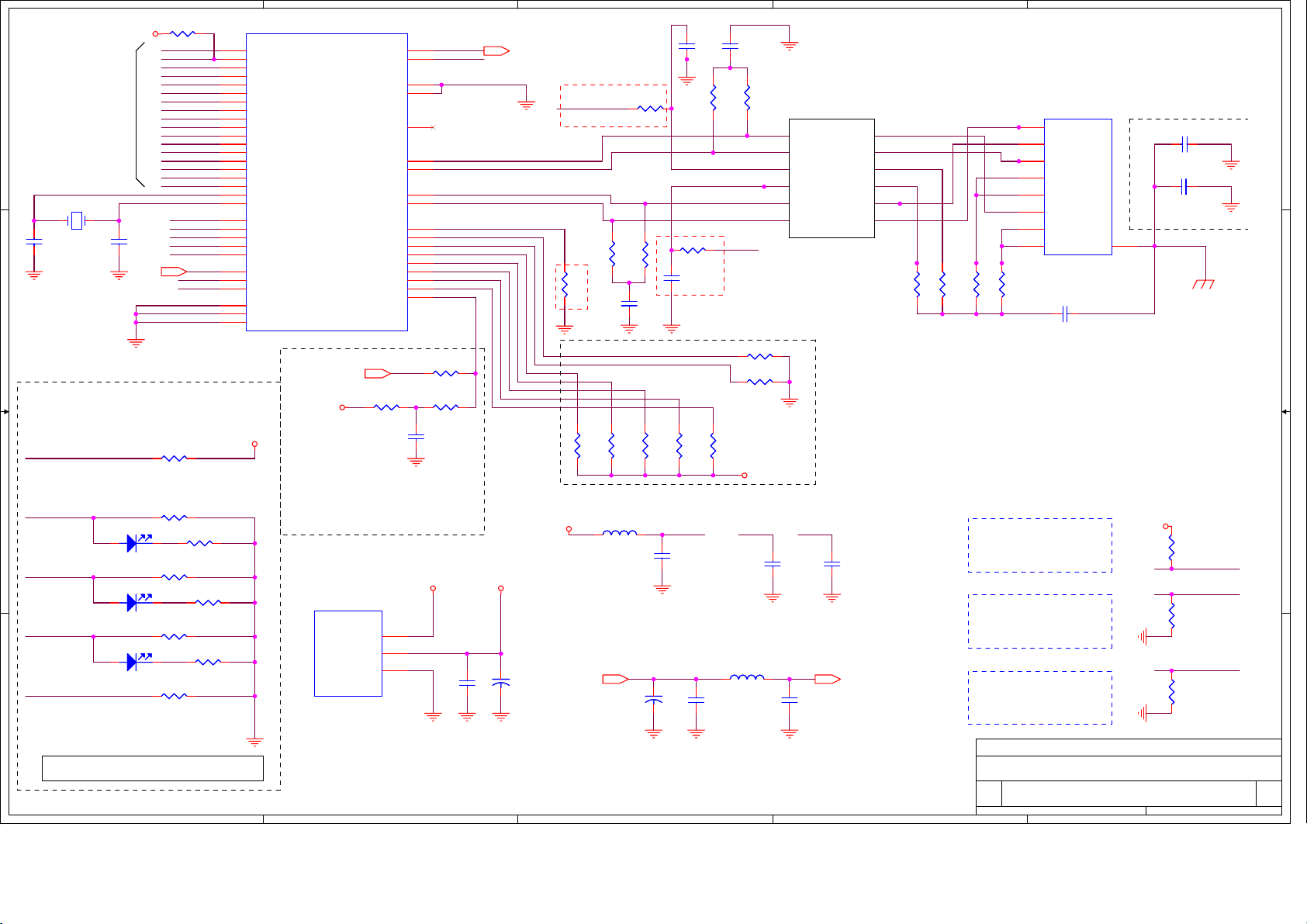
This schematic sets PHY address to 00001b.
You could set PHY address from 00001b to 11111b.
But the LED polarity must matchs the respective
PHYAD setting. Refer to datasheet's detailed
description.
LED0/PHYAD0
LED1/PHYAD1
2 2
D2
LEDD2LED
LED2/PHYAD2
D3
LEDD3LED
LED3/PHYAD3
D4
LEDD4LED
LED4/PHYAD4
1 1
LED0 LED1 LED2 LED3 LED4
Link Dupx 10Act 100Act COL
U1
25
MDC
26
MDIO
6
TXD0
5
TXD1
4
TXD2
3
TXD3
2
TXEN
7
TXC
22
RXDV
21
RXD0
20
RXD1
19
RXD2
18
RXD3
16
RXC
1
COL
23
CRS
24
RXER/FXEN
46
X1
47
X2
9
LED0/PHYAD0
10
LED1/PHYAD1
12
LED2/PHYAD2
13
LED3/PHYAD3
15
LED4/PHYAD4
8
PWFBIN
14
DVDD33
48
DVDD33
11
DGND
17
DGND
45
DGND
VDD33
GND
RTL8201BL /
RTL8201CL /
RTL8201CP
PCI_Reset
VDD33
1. You could simply connect RESETB to PCI
Reset. And just discard R30, R28, C20.
2. If Wake on Lan feature is needed, you have
to supply power from auxiliary power for all
LAN-related circuit including RTL8201BL/CL/CP
and MAC. In this kind of application, discard
R29 and retain other components for one
resetting upon power up.
U4
LM1117U4LM1117
PWFBOUT
AVDD33
ISOLATE
DUPLEX
MII/SNIB/RTT3
RESETB
INPUT
OUTPUT
ADJ/GND
B
AGND
AGND
NC
TPRXTPRX+
TPTX-
TPTX+
RTSET
RPTR
SPEED
ANE
LDPS
LQFP48U1LQFP48
R28
R28
5.1K
5.1K
3
2
1
B
32
36
29
35
27
30
31
33
34
RTL8201BL : R5 (5.9K 1%)
RTL8201CL/RTL8201CP : R5 (2K 1%)
28
43
40
39
38
37
41
44
42
R290R29
0
R300R30
0
C20
C20
0.1U
0.1U
GND
5VDD VDD33
C12
C12
0.1U
0.1U
GND
GNDGND
PWFBOUT
GND
C13
C13
22U
22U
C
C1
C2
0.1UC20.1U
R60R6
GND
R15
R15
5.1K
5.1K
AVDD33
C17
C17
0.1U
0.1U
GND
C14
C14
22U
22U
GND GND
C
C10
C10
0.1U
0.1U
0.1UC10.1U
GND
R1
R2
50(1%)R250(1%)
50(1%)R150(1%)
0
PWFBOUT
RTL8201BL : R6(NC); C10(NC)
RTL8201CL/CP : R6(0 ohm); C10(0.1uF)
R11
R11
5.1K
5.1K
R12
R12
5.1K
5.1K
R16
R16
R17
R17
5.1K
5.1K
5.1K
5.1K
VDD33
U1/pin14 U1/pin48
VDD33
GND
L1
BEADL1BEAD
C15
C15
0.1U
0.1U
RTL8201BL : R19(NC)
RTL8201CL/CP : R19(0 ohm)
R3
L2
BEADL2BEAD
50(1%)R450(1%)
R14
R14
5.1K
5.1K
R4
GND
R190R19
0
C8
0.1UC80.1U
PWFBOUT
50(1%)R350(1%)
R5R5
GND
R13
R13
5.1K
5.1K
VDD33
Place L2, C17, C18, C19 as close to each power pin
as possible.
PWFBOUT
Place C14, C15, L1 close to PWFBOUT and place C16
close to PWFBIN.
D
Reference Transformer Part No. list
YL18-2050S
GND
YuTai Electronics Co.,LTD
TEL:86-574-63620701,63621610
http;//www.yutai-elec.com
EMAIL
:
U2
8
RD-
6
RD+
7
RDCT
2
TDCT TXCT
3
TD- TX-
1
TD+
RXCT
RX-
RX+
TX+
9
11
10
15
14
16
YL18-2050S
R775R7
75
Hardwire Configuration network:
GND
1. This configuration shows
Enable: Auto negotiation, Full duplex, 100Mbps,
Link Down Power Saving, MII interface
Disable: Isolate, Repeater mode
2. These seven configuration pins could be connected to VDD
or GND directly.
VDD33
C18
C18
0.1U
0.1U
GND
C16
C16
0.1U
0.1U
C19
C19
0.1U
0.1U
GND
PWFBIN
D
R975R9
R875R8
75
R1075R10
75
75
R27 is reserved for
8201CL/CP LED Mode
Change to compatible
with BL
R34 is reserved for
ensuring 8201BL/CL/CP
latch to UTP Mode.
R35 is reserved for
ensuring 8201CL/CP
latch to normal
operation mode.
Title
Title
Title
RTL8201BL/CL/CP application circuit - interface with MAC(MII)
RTL8201BL/CL/CP application circuit - interface with MAC(MII)
RTL8201BL/CL/CP application circuit - interface with MAC(MII)
Size Document Number Rev
Size Document Number Rev
Size Document Number Rev
RTL8201BL/CL/CP MII 1.5
B
RTL8201BL/CL/CP MII 1.5
B
RTL8201BL/CL/CP MII 1.5
B
Date: Sheet
Date: Sheet
Date: Sheet
U3
1
TX+
2
TX-
3
RX+
4
N/C
5
N/C
6
RX-
7
N/C
N/C8GND
RJ8-45U3RJ8-45
C9
C9
0.01U/3KV
0.01U/3KV
E
for EMI supression
C3
0.1UC30.1U
C4
0.1UC40.1U
9
(CONNECT TO CHASSIS GND)
VDD33
R27
R27
5.1K
5.1K
R34
R34
5.1K
5.1K
GND
R35
R35
5.1K
5.1K
GND
11Thursday, November 26, 2009
11Thursday, November 26, 2009
11Thursday, November 26, 2009
E
CH_GND
COL
RXER
CRS
of
of
of
GND
GND
 Loading...