

Page 1
W24257
CS
WE
OE
32K × 8 CMOS STATIC RAM
8GENERAL DESCRIPTION
The W24257 is a slow speed, low power CMOS static RAM organized as 32768 × 8 bits that operates
on a single 5-volt power supply. This device is manufactured using Winbond's high performance
CMOS technology.
FEATURES
• Low power consumption:
− Active: 400 mW (max.)
− Standby: 250 µW (max.) (LL-version)
500 µW (max.) (L-version)
• Access time: 70/100 nS (max.)
• Single +5V power supply
• Fully static operation
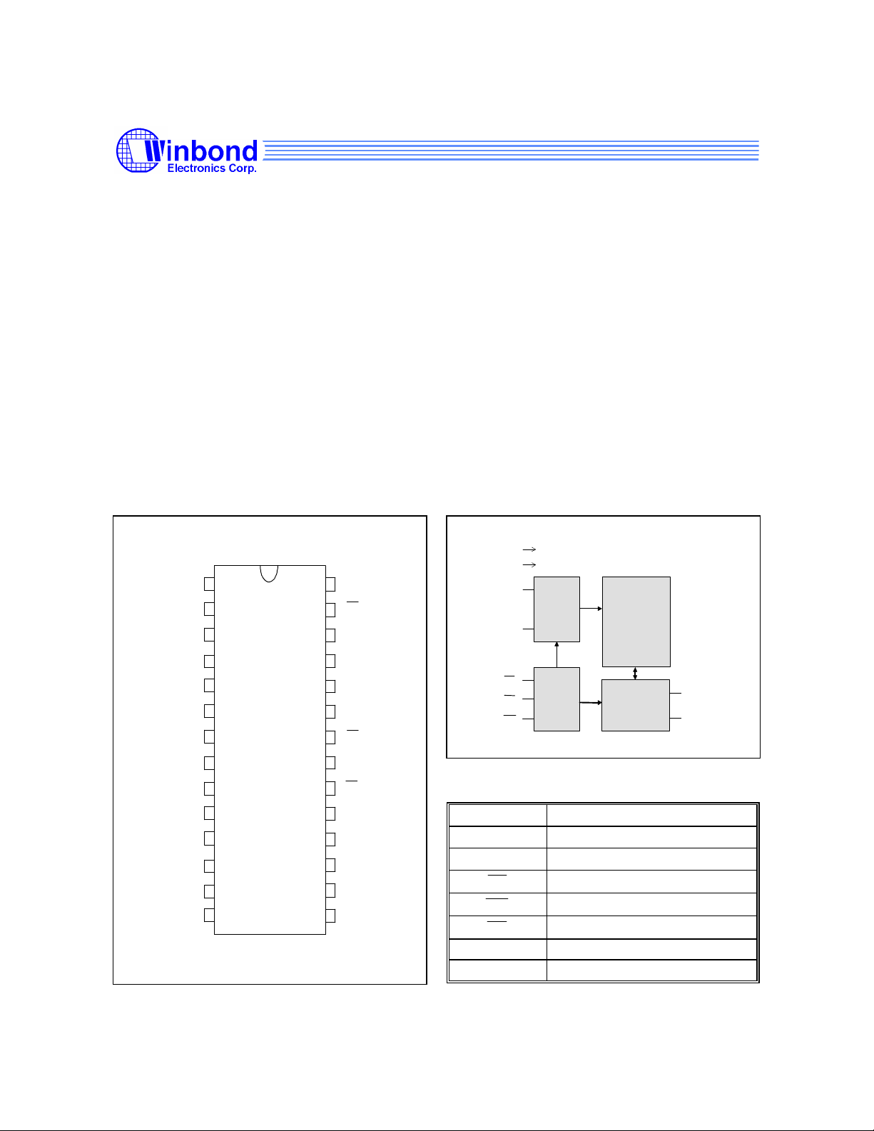
PIN CONFIGURATION
A14
A12
1
2
3
A7
4
A6
5
A5
A4
6
7
A3
8
A2
28
27
26
25
24
23
22
21
V
WE
A13
A8
A9
A11
OE
A10
• All inputs and outputs directly TTL compatible
• Three-state outputs
• Battery back-up operation capability
• Data retention voltage: 2V (min.)
• Available packages: 28-pin 600 mil DIP, 330
mil SOP, 300 mil skinny DIP and SOJ
BLOCK DIAGRAM
V
DD
SS
V
DD
A14
CS
OE
WE
A0
.
DECODER
.
CONTROL
CORE
ARRAY
DATA I/O
I/O1
I/O8
.
.
I/O1
I/O2
I/O3
A1
9
A0
10
11
12
13
V
14
SS
20
CS
19
I/O8
I/O7
18
I/O6
17
16
I/O5
I/O4
15
PIN DESCRIPTION
SYMBOL DESCRIPTION
A0−A14
I/O1−I/O8
Address Inputs
Data Inputs/Outputs
Chip Select Input
Write Enable Input
Output Enable Input
VDD Power Supply
VSS Ground
Publication Release Date: April 1997
- 1 - Revision A11
Page 2
TRUTH TABLE
CSOEWE
WE
Operating Power
CS
Supply Current
CS
CS
W24257
MODE
H X X Not Selected High Z ISB, ISB1
L H H Output Disable High Z IDD
L L H Read Data Out IDD
L X L Write Data In IDD
I/O1−I/O8
VDD CURRENT
DC CHARACTERISTICS
Absolute Maximum Ratings
PARAMETER RATING UNIT
Supply Voltage to VSS Potential -0.5 to +7.0 V
Input/Output to VSS Potential -0.5 to VDD +0.5 V
Allowable Power Dissipation 1.0 W
Storage Temperature -65 to +150
Operating Temperature 0 to +70
Note: Exposure to conditions beyond those listed under Absolute Maximum Ratings may adversely affect the life and reliability of the
device.
Operating Characteristics
(VDD = 5V ±10%, VSS = 0V, TA = 0 to 70° C)
PARAMETER SYM. TEST CONDITIONS MIN. TYP. MAX. UNIT
Input Low Voltage VIL - -0.5 - +0.8 V
Input High Voltage VIH - +2.2 - VDD +0.5 V
Input Leakage Current ILI VIN = VSS to VDD -2 - +2
Output Leakage
Current
Output Low Voltage VOL IOL = +4.0 mA - - 0.4 V
Output High Voltage VOH IOH = -1.0 mA 2.4 - - V
Standby Power
Supply Current
Note: Typical characteristics are at VDD = 5V, TA = 25° C.
ILO
IDD
ISB
ISB1
VI/O = VSS to VDD, CS = VIH
(min.) or OE = VIH (min.) or
= VIL (max.)
= VIL (min.),
I/O = 0 mA
Cycle = min.,
Duty = 100%
= VIH (min.)
Cycle = min., Duty = 100%
≥ VDD -0.2V
-2 - + 2
70 - - 80 mA
100 - - 70 mA
- - 3 mA
LL - - 50
L - - 100
°C
°C
µA
µA
µA
µA
- 2 -
Page 3
W24257
CAPACITANCE
(VDD = 5V, TA = 25° C, f = 1 MHz)
PARAMETER SYM. CONDITIONS MAX. UNIT
Input Capacitance CIN VIN = 0V 6 pF
Input/Output Capacitance CI/O VOUT = 0V 8 pF
Note: These parameters are sampled but not 100% tested.
AC CHARACTERISTICS
AC Test Conditions
PARAMETER CONDITIONS
Input Pulse Levels 0.6V to 2.4V
Input Rise and Fall Times 5 nS
Input and Output Timing Reference Level 1.5V
Output Load CL = 100 pF, IOH/IOL = -1 mA/4 mA
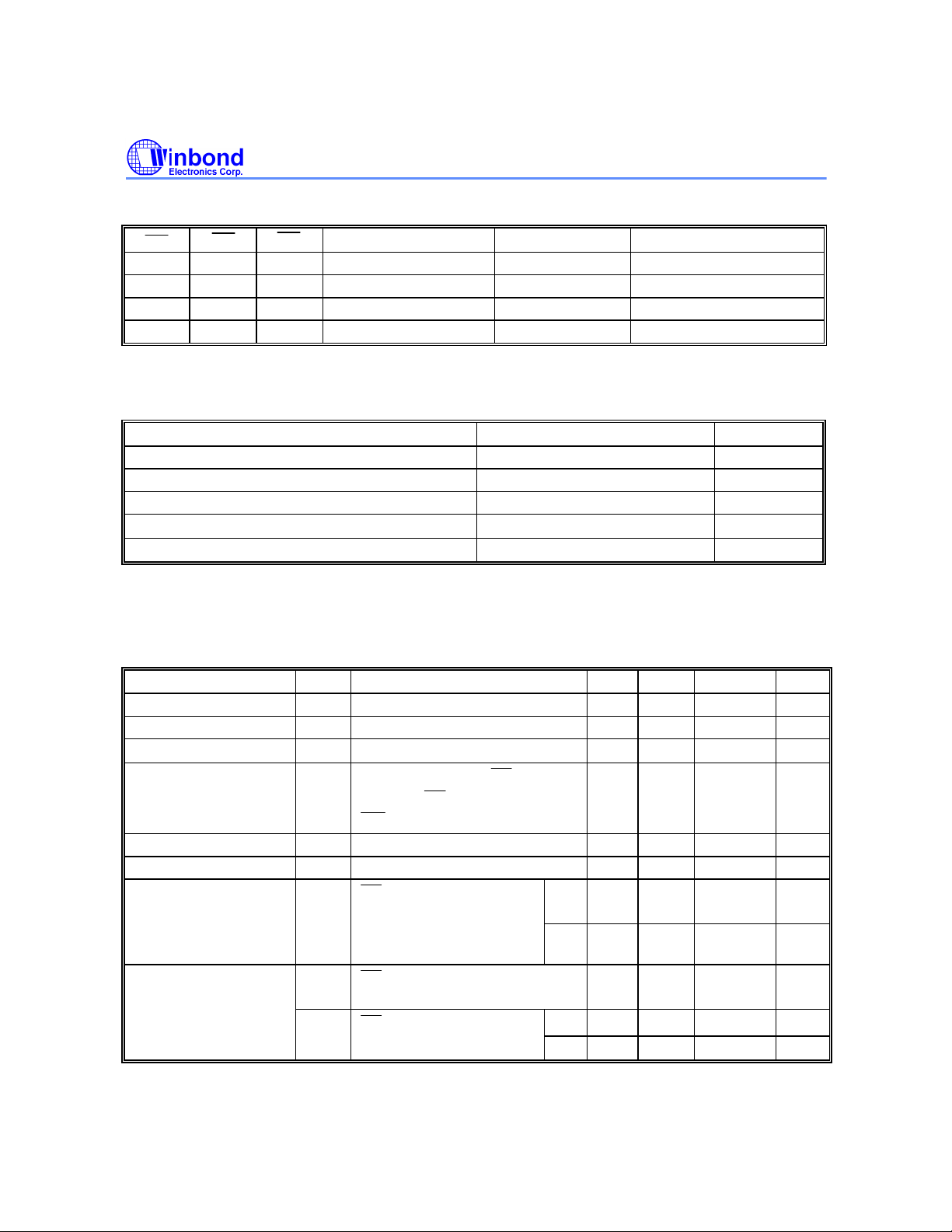
AC Test Loads and Waveform
R1 1000 ohm
5V
OUTPUT
100 pF
Including
Jig and
Scope
R2
660 ohm
3.0V
0V
5 nS
90% 90%
10%
10%
OUTPUT
(For T
5 nS
5V
CLZ
OLZ TCHZ T
, ,
T
,
R1 1000 ohm
5 pF
Including
Jig and
Scope
OHZ
,
T
WHZ
R2
660 ohm
,
)
OW
T
Publication Release Date: April 1997
- 3 - Revision A11
Page 4
W24257
CS, WE
AC Characteristics, continued
(VDD = 5V ±10%, VSS = 0V, TA = 0 to 70° C)
Read Cycle
PARAMETER SYM. W24257-70 W24257-10 UNIT
MIN. MAX. MIN. MAX.
Read Cycle Time TRC 70 - 100 - nS
Address Access Time TAA - 70 - 100 nS
Chip Select Access Time TACS - 70 - 100 nS
Output Enable to Output Valid TAOE - 35 - 50 nS
Chip Selection to Output in Low Z TCLZ* 10 - 10 - nS
Output Enable to Output in Low Z TOLZ* 5 - 5 - nS
Chip Deselection to Output in High Z TCHZ* - 30 - 35 nS
Output Disable to Output in High Z TOHZ* - 30 - 35 nS
Output Hold from Address Change TOH 10 - 10 - nS
∗ These parameters are sampled but not 100% tested
Write Cycle
PARAMETER SYM. W24257-70 W24257-10 UNIT
MIN. MAX. MIN. MAX.
Write Cycle Time TWC 70 - 100 - nS
Chip Selection to End of Write TCW 60 - 80 - nS
Address Valid to End of Write TAW 60 - 80 - nS
Address Setup Time TAS 0 - 0 - nS
Write Pulse Width TWP 45 - 60 - nS
Write Recovery Time
Data Valid to End of Write TDW 30 - 40 - nS
Data Hold from End of Write TDH 0 - 0 - nS
Write to Output in High Z TWHZ* - 30 - 30 nS
Output Disable to Output in High Z TOHZ* - 30 - 30 nS
Output Active from End of Write TOW 0 - 0 - nS
∗ These parameters are sampled but not 100% tested
TWR 0 - 0 - nS
- 4 -
Page 5

TIMING WAVEFORMS
AA
Read Cycle 1
(Address Controlled)
Address
DOUT
Read Cycle 2
(Chip Select Controlled)
W24257
T
RC
T
T
OH
T
OH
CS
D
OUT
Read Cycle 3
(Output Enable Controlled)
Address
OE
CS
D
OUT
T
ACS
T
CLZ
RC
T
T
AA
AOE
T
TOLZ
TACS
CLZT
T
CHZ
TOH
TOHZ
CHZ
T
Publication Release Date: April 1997
- 5 - Revision A11
Page 6

Timing Waveforms, continued
Write Cycle 1
Address
OE
CS
WE
DOUT
DIN
W24257
T
WC
T
WR
T
CW
T
AW
T
T
AS
T
OHZ
(1, 4)
WP
T
DW
T
DH
Write Cycle 2
(OE = VIL Fixed)
T
WC
Address
T
T
CW
CS
AWT
WE
D
OUT
DIN
T
AS
T
WP
T
WHZ
(1, 4)
Notes:
1. During this period, I/O pins are in the output state, so input signals of opposite phase to the outputs should not be applied.
2. The data output from DOUT are the same as the data written to DIN during the write cycle.
3. DOUT provides the read data for the next address.
4. Transition is measured ±500 mV from steady state with CL = 5 pF. This parameter is guaranteed but not 100% tested.
WR
T
OH
T
OW
DW
TDH
T
(2) (3)
- 6 -
Page 7

W24257
CS
CS
DATA RETENTION CHARACTERISTICS
(TA = 0 to 70° C)
PARAMETER SYM. TEST CONDITIONS MIN. TYP. MAX. UNIT
VDD for Data Retention VDR
Data Retention Current IDDDR
≥ VDD -0.2V
≥ VDD -0.2V
VDD = 3V L - - 50
Chip Deselect to Data Retention Time TCDR See data retention 0 - - nS
Operation Recovery Time TR waveform TRC* - - nS
TRC* = Read Cycle Time
DATA RETENTION WAVEFORM
DATA RETENTION MODE
V
CS
DD
4.5V
T
CDR
VIH V
CS1
>
V
DR
2V
=
>
V
DD
=
-0.2V
4.5V
T
R
IH
2.0 - - V
LL - - 20
µA
µA
ORDERING INFORMATION
PART NO. ACCESS
TIME (nS)
W24257-70LL 70 80 50 600 mil DIP
W24257-70L 70 80 100 600 mil DIP
W24257-10L 100 70 100 600 mil DIP
W24257S-70LL 70 80 50 330 mil SOP
W24257S-70L 70 80 100 330 mil SOP
W24257S-10L 100 70 100 330 mil SOP
W24257K-70LL 70 80 50 300 mil Skinny
W24257K-70L 70 80 100 300 mil Skinny
W24257K-10L 100 70 100 300 mil Skinny
W24257J-70LL 70 80 50 300 mil SOJ
W24257J-70L 70 80 100 300 mil SOJ
W24257J-10L 100 70 100 300 mil SOJ
Notes:
1. Winbond reserves the right to make changes to its products without prior notice.
2. Purchasers are responsible for performing appropriate quality assurance testing on products intended for use in
applications where personal injury might occur as a consequence of product failure.
OPERATING
CURRENT
MAX. (mA)
STANDBY
CURRENT
MAX. (mA)
PACKAGE
Publication Release Date: April 1997
- 7 - Revision A11
Page 8

BONDING PAD DIAGRAM
W24257
4
6
A4 A13
7
A3
8
9A110
A2
3
5
A5
A6
Y
11
12 13
A0 I/O1 I/O2 I/O3
12
28
S-228S-1
DD
A14A12A7
DDV
X
14
S-2
14
S-1
SS
V
I/O4
SS
V
27
15 16
I/O5
I/O6
23
242526
A11
A8WEV
A9
22
OE
PAD NO. X Y
1 -127.08 2785.05
2 -377.73 2785.05
3 -628.38 2785.05
4 -879.03 2785.05
5 -1129.68 2785.05
6 -1380.33 2785.05
7 -1686.51 2640.06
8 -1682.01 -2645.91
9 -1448.10 -2802.51
10 -1090.80 -2802.51
11 -877.32 -2807.28
12 -627.84 -2807.28
13 -349.56 -2807.28
14S-1 -155.52 -2781.00
14S-2 -7.02 -2771.64
21
A10
20
18
19
17
CS
I/O8
I/O7
15 249.21 -2807.28
16 498.69 -2807.28
17 776.97 -2807.28
18 1026.45 -2807.28
19 1304.73 -2807.28
20 1689.30 -2802.51
21 1686.51 -2520.90
22 1686.51 2644.74
23 1459.17 2785.05
24 1208.52 2785.05
25 957.87 2785.05
26 707.22 2785.05
27 456.57 2785.05
28S-1 205.92 2771.55
28S-2 21.42 2780.91
Note: For bare chip form (C.O.B.) applications, the substrate must be connected to VDD or left floating in the PCB layout.
- 8 -
Page 9

PACKAGE DIMENSIONS
28-pin P-DIP
W24257
28
E
1
1
S
2
A
A
L
28-pin P-DIP Skinny
28
1E
1 14
S
A
A
2
L
Dimension in Inches
Symbol
Min. Nom. Max. Max.Nom.Min.
A
0.010
1
A
0.150
2
1
1
1
A
0.016
0.008
0.540 0.5500.545
0.090
0.120
0 15
0.155
0.018
0.060 1.52
0.010
1.460 1.470
0.6000.590
0.100
0.130
0.6500.630 16.00 16.51
A
B
B
c
D
15
D
E
E
e
L
a
e
S
14
E
A
1
Base Plane
15
Seating Plane
Base Plane
1A
Mounting Plane
e
a
A
E
e
A
a
c
B
e
1
B
1
D
B
B
e
1
1
Notes:
1. Dimension D Max. & S include mold flash or
tie bar burrs.
c
2. Dimension E1 does not include interlead flash.
3. Dimension D & E1 include mold mismatch and
are determined at the mold parting line.
4. Dimension B1 does not include dambar
protrusion/intrusion.
5. Controlling dimension: Inches.
6. General appearance spec. should be based on
final visual inspection spec.
Dimension in Inches Dimension in mm
Symbol
Min. Nom. Max. Max.Nom.Min.
A
0.010
A
1
0.130
0.125
A
2
0.016
B
B1
c
D
E
E
e
L
a
e
S
Notes:
1. Dimension D Max. & S include mold flash or
tie bar burrs.
2. Dimension E1 does not include interlead flash.
3. Dimension D & E1 include mold mismatch and
are determined at the mold parting line.
4. Dimension B1 does not include dambar
protrusion/intrusion.
5. Controlling dimension: Inches.
6. General appearance spec. should be based on
final visual inspection spec.
0.018
0.060 1.52
0.010
0.008
1.388 1.400
0.3100.300 0.320
0.2880.283
1
1
0.120
0.130
°
0
0.330 8.38
0.350
A
Dimension in mm
0.210
0.160
0.022
0.0640.058
0.014
0.610
14.99
13.72 13.9713.84
0.110
0.140
0.670
0.090 2.29
5.33
0.25
3.81
3.94
4.06
0.41
0.46
0.56
0.20
0.25
37.34
37.08
15.49
15.24
2.29
2.54 2.79
3.05
3.30
17.02
.
0.175
0.25
0.135
3.18
3.30
0.41
0.022
0.0640.058
0.014
0.293
0.110
0.140
0.370
0.055
15
0.46
0.20
0.25
35.26 35.56
7.87
7.62
7.19
2.29 2.54 2.790.090 0.100
3.05
3.30
°
°
0
8.89
1.631.47
0.36
3.56
150
4.45
3.43
0.56
1.631.47
0.36
8.13
7.447.32
3.56
°
15
9.40
1.40
Publication Release Date: April 1997
- 9 - Revision A11
Page 10

Package Dimensions, continued
28-pin SO Wide Body
W24257
28 15
1
S
Seating Plane
e
b
D
y
28-pin Small Outline J Band
1
D
s
Seating Plane
b
1b
e
Dimension in Inches
Symbol
A
A
e
1
E H
E
L
e
1
See Detail F
Detail F
c
L
E
14
A
A
2
A
1
A
b
c
D
E
e
HE
L
LE
S
y
θ
Notes:
1. Dimension D Max. & S include mold flash
or tie bar burrs.
2. Dimension b does not include dambar
protrusion/intrusion.
3. Dimension D & E include mold mismatch
and determined at the mold parting line.
4. Controlling dimension: Inches.
5. General appearance spec should be based
on final visual inspection spec.
Symbol
1528
EHE
14
Notes:
2
A
A
L
£c
1
A
y
1e
c
Nom.
Min.
0.004
1
0.098
0.093
2
0.014
0.016
0.0100.008
0.713
0.028
0.036
0.059
0.067
0
Dimension in Inches
Min. Nom. Max. Max.Nom.Min.
A
0.027
1
A
0.095
A
2
0.026
b1
0.016
b
0.008
c
D
0.295
E
0.044
e
0.245
1
e
0.327
H
E
0.077
L
S
y
θ
0
1. Dimension D Max. & S include mold flash
or tie bar burrs.
2. Dimension b does not include dambar
protrusion/intrusion.
3. Dimension D & E include mold mismatch
and are determined at the mold parting line.
4. Controlling dimension: Inches.
5. General appearance spec. should be based
on final visual inspection spec.
Dimension in mm
Nom.
Max. Max.
Min.
0.112
0.10
0.103
2.36
2.49
0.36
0.020
0.014 0.36
0.733
0.3360.3310.326
0.4770.4650.453 12.1211.8111.51
0.044
0.075 1.50
0.047
0.004
0.41
0.250.20
18.11
8.28
8.41
1.12 1.27 1.420.044 0.050 0.056
0.91 1.12
0.71
1.70
10
0
.
Dimension in mm
0.140
0.105
0.0320.028
0.022
0.014
0.730
0.3050.300
0.285
0.347
0.097 1.96
0.045
0.004
10
0.69
2.41
0.41
7.49
1.12
6.22
8.31
0
18.03
7.62
1.27
8.56 8.81
2.21
0.100
0.018
0.010 0.25
0.710
0.050 0.056
0.265
0.337
0.087
2.85
2.62
0.51
18.62
8.53
1.91
1.19
0.10
10
3.56
2.54
2.67
0.810.710.66
0.46
0.56
0.360.20
18.54
7.75
1.42
7.246.73
2.46
1.14
0.10
10
- 10 -
Page 11

W24257
Headquarters
No. 4, Creation Rd. III,
Science-Based Industrial Park,
Hsinchu, Taiwan
TEL: 886-3-5770066
FAX: 886-3-5792647
http://www.winbond.com.tw/
Voice & Fax-on-demand: 886-2-7197006
Taipei Office
11F, No. 115, Sec. 3, Min-Sheng East Rd.,
Taipei, Taiwan
TEL: 886-2-7190505
FAX: 886-2-7197502
Winbond Electronics (H.K.) Ltd.
Rm. 803, World Trade Square, Tower II,
123 Hoi Bun Rd., Kwun Tong,
Kowloon, Hong Kong
TEL: 852-27513100
FAX: 852-27552064
Winbond Electronics North America Corp.
Winbond Memory Lab.
Winbond Microelectronics Corp.
Winbond Systems Lab.
2727 N. First Street, San Jose,
CA 95134, U.S.A.
TEL: 1-408-9436666
FAX: 1-408-5441798
Note: All data and specifications are subject to change without notice.
Publication Release Date: January 1997
- 11 - Revision A11
 Loading...