

Features
• Frequency Receiving Range of
f
= 868 MHz to 870 MHz or f0=902MHz to 928MHz
0
•
30 dB Image Rejection
• Receiving Bandwidth B
• Fully Integrated LC-VCO and PLL Loop Filter
• Very High Sensitivity with Power Matched LNA
• High System IIP3 (-16 dBm), System 1-dB Compression Point (-25 dBm)
• High Large-signal Capability at GSM Band
(Blocking -30 dBm at +20 MHz, IIP3 = -12 dBm at +20 MHz)
• 5 V to 20 V Automotive Compatible Data Interface
• Data Clock Available for Manchester- and Bi-phase-coded Signals
• Programmable Digital Noise Suppression
• Low Power Consumption Due to Configurable Polling
• Temperature Range -40°C to +105°C
• ESD Protection 2 kV HBM, All Pins
• Communication to Microcontroller Possible Via a Single Bi-directional Data Line
• Low-cost Solution Due to High Integration Level with Minimum External Circuitry
Requirements
= 600 kHz for Low Cost 90-ppm Crystals
IF
UHF ASK/FSK
Receiver
T5760/T5761
Description
The T5760/T5761 is a multi-chi p PLL recei ver device supplied in an SO20 pa ckage. It
has been especially developed for the demands of RF low-cost data transmission
systems with data rates from 1 kBaud to 10 kBaud in Manchester or Bi-phase code.
The receiver is well suited to operate with the Atmel’s PLL RF transmitter T5750. Its
main applications are in the areas of telemetering, securi ty technology and keylessentry systems. It can be used in the frequency receiving range of f
870 MHz or f
= 902 MHz to 928 MHz for ASK or FSK data transmission. All the state-
0
ments made below refer to 868.3 MHz and 915.0 MHz applications.
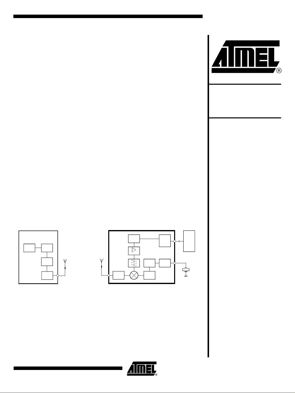
Figure 1. System Block Diagram
UHF ASK/FSK
Remote control transmitter
T5750
XTO
PLL
VCO
Power
amp.
Antenna
T5760/
T5761
Antenna
LNA VCO
UHF ASK/FSK
Remote control receiver
Demod.
IF Amp
PLL XTO
= 868 MHz to
0
Control
1...5
µC
Preliminary
Rev. 4561B–RKE–10/02
1
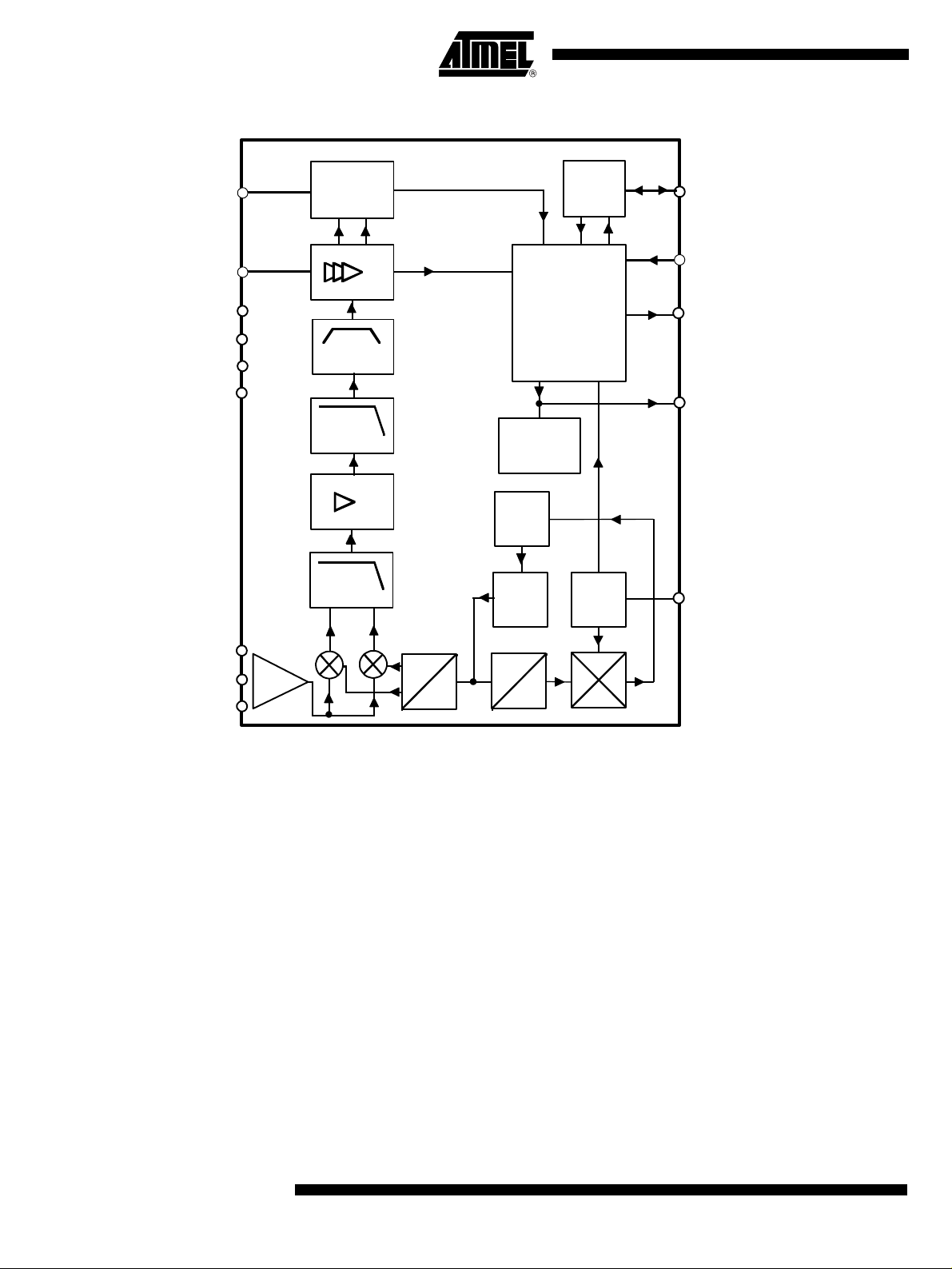
Figure 2. Block Diagram
CDEM
SENS
AVCC
AGND
DGND
DVCC
FSK/ASK-
demodulator
and data filter
Rssi Limiter out
RSSI IF
Amp.
4. Order
f0 = 950 kHz/
1 MHz
LPF
fg = 2.2 MHz
IF
Amp.
Poly-LPF
fg = 7 MHz
Dem_out
Sensitivity-
reduction
Polling circuit
control logic
FE CLK
Standby logic
Loop-
filter
LC-VCO
interface
and
Data -
XTO
DATA
POLLING/_ON
DATA_CLK
IC_ACTIVE
XTAL
LNAREF
LNA_IN
LNAGND
LNA
f
:2
f
:256
2
T5760/T5761
4561B–RKE–10/02
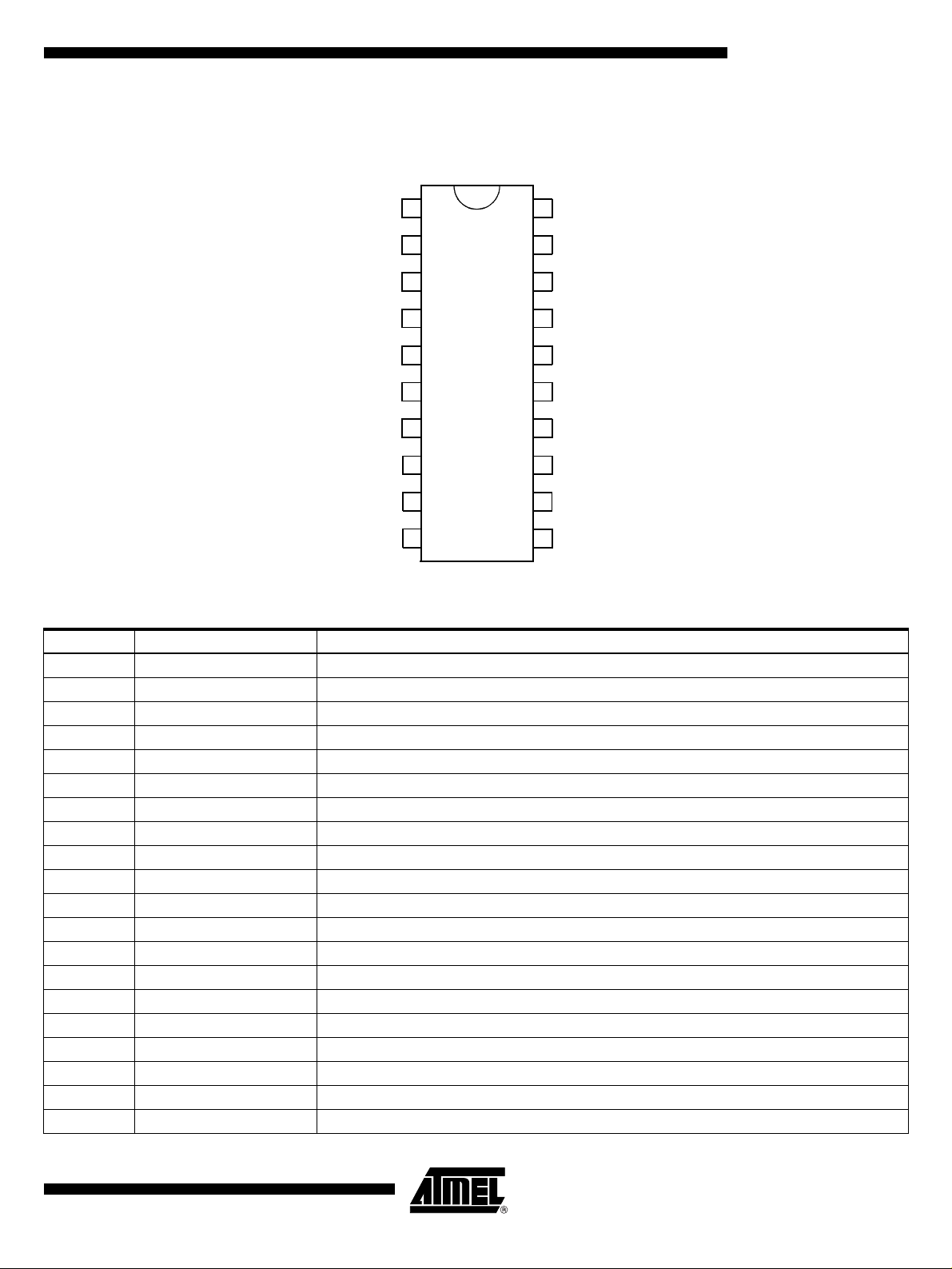
Pin Configuration
Figure 3. Pinning SO20
T5760/T5761
SENS
IC_ACTIVE
CDEM
AVCC
TEST 1
1
2
3
4
5
20
DATA
19
POLLING/_ON
18
DGND
17
DATA_CLK
16
TEST 4
T5760/
AGND
n.c.
LNAREF
LNA_IN
LNAGND
T5761
6
7
8
9
10
15
DVCC
14
XTAL
13
n.c.
12
TEST 3
11
TEST 2
Pin Description
Pin Symbol Function
1 SENS Sensitivity-control resistor
2 IC_ACTIVE IC condition indicator: Low = sleep mode, High = active mode
3 CDEM Lower cut-off frequency data filter
4 AVCC Analog power supply
5 TEST 1 Test pin, during operation at GND
6 AGND Analog ground
7 n.c. Not connected, conne ct to GND
8 LNAREF High-frequency reference node LNA and mixer
9 LNA_IN RF input
10 LNAGND DC ground LNA and mixer
11 TEST 2 Do not connect during operating
12 TEST 3 Test pin, during operation at GND
13 n.c. Not connected, conne ct to GND
14 XTAL Crystal oscillator XTAL connection
15 DVCC Digital power supply
16 TEST 4 Test pin, during operation at DVCC
17 DATA_CLK Bit clock of data stream
18 DGND Digital ground
19 POLLING/_ON Selects polling or receiving mode; Low: receiving mode, High: polling mode
20 DATA Data output/configuration input
4561B–RKE–10/02
3
RF Front End The RF front end of the receiver is a low-IF heterodyne configuration that converts the
input signal into a 950 kHz/1 MHz IF signal with an image rejection of typical 30 dB.
According to Figure 3 the front end consis ts of an LNA (Lo w Nois e Amp lifie r), LO (Lo cal
Oscillator), I/Q mixer, polyphase lowpass filter and an IF amplifier.
The PLL generates the carrier frequency for the mixer via a full integrated synthesizer
with integrated lo w noise LC- VCO (Voltage Co ntrolle d Oscillat or) and PLL-l oop filter .
The XTO (crystal oscillator ) generates t he reference fr equenc y f
VCO generate s two t imes t he mix er driv e freq uency f
are generated with a divide by two circuit (f
LO
= f
VCO
. The I/Q signals for the mixer
VCO
/2). f
is divided by a factor of 256
VCO
and feeds into a phase frequency detector and compared with f
phase frequency detector is fed into an i ntegrat ed loop filte r and thereb y gener ates the
control voltage for the VCO. If f
is determined, f
LO
can be calculated using the follow-
XTO
ing formula:
f
= fLO/128
XTO
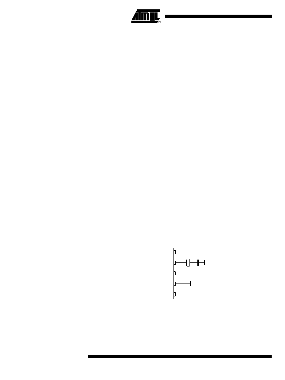
The XTO is a on e-pin osci llator that op erates at the series resonance o f the quartz
crystal with high current but low voltage signal, so that there is only a small voltage at
the crystal oscillator frequency at Pin XTAL. According to Figure 4, the crystal should be
connected to GND with a se ries capacitor C
. The value of that cap acitor is rec om-
L
mended by the crystal supplier. Due to a somewhat inductive impedance at steady state
oscillation and some PCB parasitics a lower value of C
The value of C
value of f
should be optimized for the ind ivid ual boa rd layou t to a chiev e th e ex act
L
(the best way is to use a crystal with known load resonance frequency to
XTO
find the right value for this capacitor) and hereby of f
is normally necessary.
L
. When designing the system in
LO
terms of receiving bandwidth and local oscillator accuracy, the accuracy of the crystal
and the XTO must be considered.
. The integrated LC-
XTO
. The output of the
XTO
If a crystal with ±30 ppm adjus tment tolerance at 25 °C, ±50 ppm over temperature
-40°C to +105°C, ±10 ppm of total aging and a CM (motional capacitance) of 7 fF is
used, an additional XTO pulling of ±30 ppm has to be added.
The resulting total LO tolerance of ±120 ppm agrees with the receiving bandwidth
specification of the T5760/T5761 if the T5750 has also a total LO tolerance of
±120 ppm.
Figure 4. XTO Peripherals
V
S
C
L
The nominal frequency f
frequency f
f
= fRF - f
LO
using the following formula (low side injection):
IF
IF
DVCC
XTAL
n.c.
TEST 3
TEST 2
is determined by the RF input frequency fRF and the IF
LO
4
T5760/T5761
4561B–RKE–10/02

T5760/T5761
To determine fLO, the construction of the IF filter must be considered at this point. The
nominal IF frequency is f
frequencies, the filter is tuned by the crystal frequency f
fixed relation between f
f
= fLO/915
IF
The relation is designed to achieve the nominal IF frequency of f
868.3 MHz version. For the 915 MHz version an IF freque nc y of f
The RF input either from an antenna or from an RF generator must be transformed to
the RF input Pin LNA_IN. The input impedance of that pin is provided in the electrica l
parameters. The parasitic board inductances and capacitances influence the input
matching. The RF receiver T5760/T5761 exhibits its highest sensitivity if the LNA is
power matched. This makes the matching to an SAW filter as well as to 50 W or an
antenna easier.
= 950 kHz. To achieve a good accurac y of the filter corner
IF
and fLO.
IF
. This means that there is a
XTO
= 950 kHz for the
IF
= 1.0 MHz results.
IF
Figure 33 shows a typical input matching network for f
= 868.3 MHz to 50 W. Figure 34
RF
illustrates an according input matching for 868.3 MHz to an SAW. The input matchi ng
network shown in Figure 33 is the reference network for the parameters given in the
electrical character isti cs .
Analog Signal Processing
IF Filter The signals coming from the RF front-end are filtered by the fully integrated 4th-order IF
filter. The IF center frequency is f
and f
=1.0 MHz for fRF = 915 MHz. The nominal bandwidth is 600 kHz.
IF
Limiting RSSI Amplifier The subsequent RSSI amplifier enhances the output signal of the IF amplifier before it is
fed into the demodulator. The dynamic range of this amplifier is DR
RSSI amplifier is operated within its linear range, the best S/N ratio is maintained in ASK
mode. If the dynamic range is exceeded by the transmitter signal, the S/N ratio is
defined by the ratio of the maximum RSSI output voltage and the RSSI output voltage
due to a disturber. The dynamic ran ge of the RSSI am plifier is exceede d if the RF input
signal is about 60 dB higher compared to the RF input signal at full sensitivity.
In FSK mode the S/N ratio is not affected by the dynamic range of the RSSI amplifier,
because only the hard limited signal fr om a h igh gain limit ing ampl ifier is used by the
demodulator.
The output voltage of the RSSI amplifier is internally compared to a threshold voltage
V
. V
Th_red
nected between Pin S ENS a nd G ND or V
digital control logic. By this means it is possible to operate the receiver at a lower
sensitivity.
is determined by the value of th e external res istor R
Th_red
= 950 kHz for applications where fRF = 868.3 MHz
IF
= 60 dB. If the
RSSI
. R
. The output of the c om par at or is f ed into the
S
Sens
Sens
is con-
4561B–RKE–10/02
If R
is connected to GND, the receiver switches to full sensitivity. It is also possible to
Sens
connect the Pin SENS directly to GND to get the maximum sensitivity.
If R
sensitivity is defined by the value of R
is connected to VS, the receiver operates at a lower sensitivity. The reduced
Sens
, the maximum sensitivity by the signal-to-
Sens
noise ratio of the LNA input. The reduced sensitivity depends on the signal strength at
the output of the RSSI amplifier.
5
Since different RF in put netw orks may ex hibit sli ghtly di fferent val ues for the LN A gain,
the sensitivity values given in the electrical characteristics refer to a specific input
matching. This matchi ng is illustr ated in Figur e 33 and exhibi ts the best poss ible sens itivity and at the same time power matching at RF_IN.
R
can be connected to VS or GND via a mic rocontrolle r. The receiver can be
Sens
switched from full sensitivity to reduced sensitivity or vice versa at any time. In polling
mode, the receiver will not wake up if the R F input signal doe s not exceed the se lected
sensitivity. If the receiver is already active, the data stream at Pin DATA will disappear
when the input signal is lower than defined by the reduced sensitivity. Instead of the
data stream, the pattern according to Figure 5 is issued at Pin DATA to indicate that the
receiver is still active (see Figure 32).
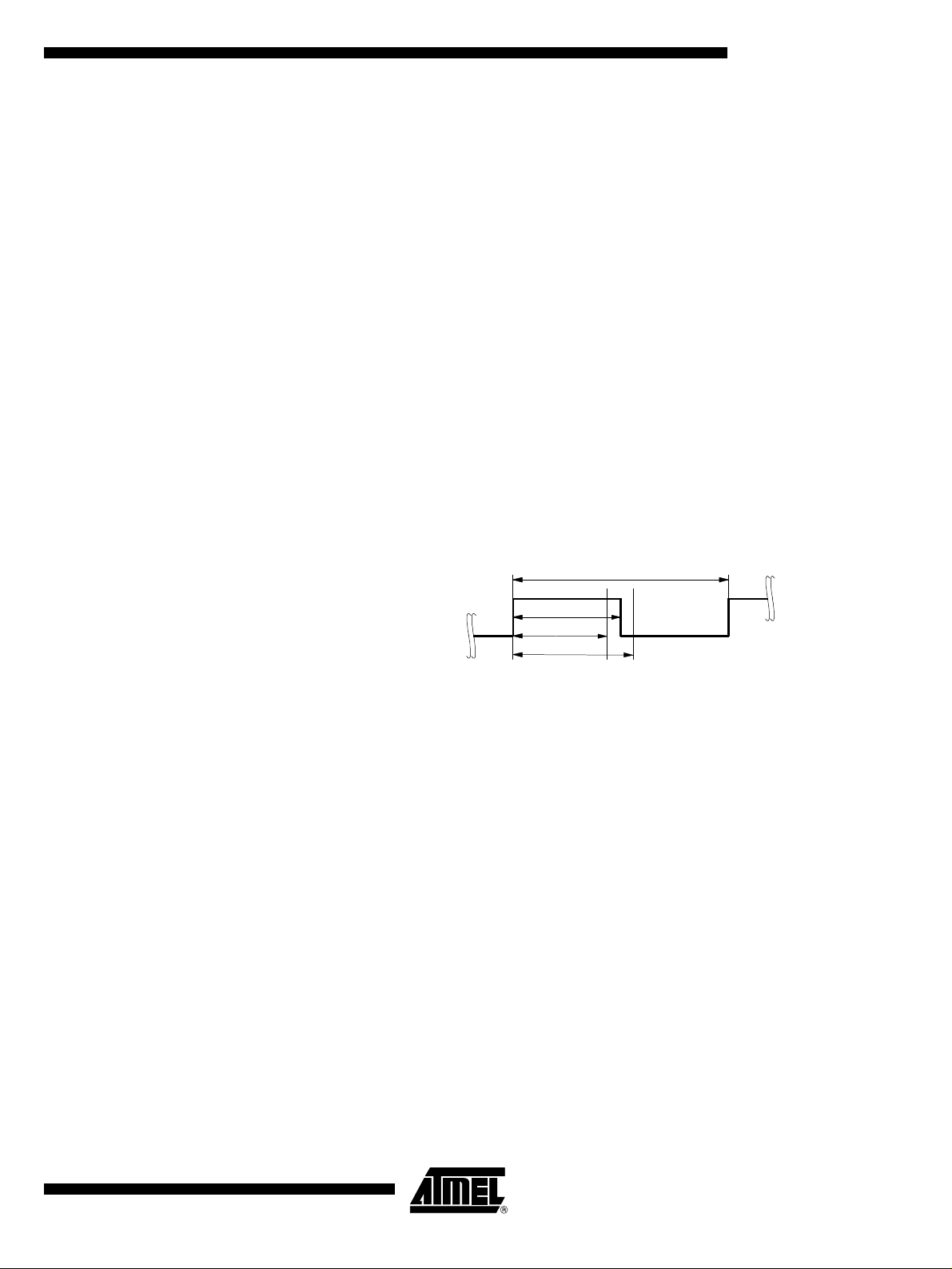
Figure 5. Steady L State Limited DATA Output Pattern
FSK/ASK Demodulator
and Data Filter
DATA
t
DATA_min
t
DATA_L_max
The signal coming from the RSSI amplifier is converted into the raw data signal by the
ASK/FSK demodulator. The operating mode of the demodulator is set via the bit
ASK/_FSK in the OPMODE register. Logic ‘L’ sets the demodulator to FSK, applying ‘H’
to ASK mode.
In ASK mode an automatic thr eshold co ntrol circuit (A TC) is e mployed to set the dete ction reference voltage to a v alue w here a good s ignal to nois e ratio is achi eved. Th is
circuit also implies the effective suppression of any kind of in-band noise signals or competing transmitters. If the S/N (ratio to suppress in-band noise signals) exceeds about
10 dB the data si gnal can be de tected p roperly, b ut better valu es are fo und f or many
modulation schemes of the competing transmitter.
The FSK demodulator is intended to be used for an FSK dev iation of 10 kHz £ Df £
100 kHz. In FSK mode the data signal can be detected if the S/N (ratio to suppress inband noise signal s) ex ceeds abou t 2 dB . This val ue is v alid for all mod ulati on sc hemes
of a disturber signal.
The output signal of the demo dulator is filtered by the data filter befo re it is fed in to the
digital signal processing circuit. The data filter improves the S/N r atio as its passband
can be adopted to the cha racter istics of the da ta signal . The data filter c onsists of a 1
order high pass and a 2
nd-
order lowpass filter.
st-
The highpass filter cut-off frequency is defined by an external capacitor connected to Pin
CDEM. The cut-off frequency of the highpass filter is defined by the following formula:
fcu_DF
-----------------------------------------------------------=
2 p´ 30 kW´ CDEM´
1
In self-polling mode , the data fil ter mu st settle very rapidly to ac hie ve a lo w cu r re nt consumption. Therefore, CDEM cannot be increased to very high values if self-polling is
used. On the other hand CDE M must b e large eno ugh to me et the dat a filter requirements according to the d ata signal. Reco mmended val ues for CDEM ar e given in th e
electrical character isti cs .
The cut-off frequenc y of the lowpass fi lter is define d by the selecte d baud-rate ra nge
(BR_Range). The BR_Range is defined in the OPMODE register (refer to chapter
‘Configuration o f the Receiv er’). The B R_Ra nge mu st be set in ac cordan ce to the u sed
baud-rate.
6
T5760/T5761
4561B–RKE–10/02
T5760/T5761
The T5760/T5761 is designed to operate with data coding where the DC level of the
data signal is 50%. This is valid for Manchester and Bi-phase coding. If other modulation
schemes are used, the DC level should always remain within the range of V
and V
= 66%. The sensitivity may be reduced by up to 2 dB in that condition.
DC_max
Each BR_Range is also defined by a minimum and a maximum edge-to-edge time
(t
). These limits are defined in the electrical characteristics. They should not be
ee_sig
exceeded to maintain full sensitivity of the receiver.
DC_min
=33%
Receiving
Characteristics
The RF receiver T5760/T5761 c an be ope rated with a nd withou t a SAW fro nt-end fil ter.
In a typical aut omo tiv e appl ication, a SAW fi lte r is u sed to ac hi ev e b ette r selectivity and
large signal capab ility. T he rec eivi ng frequen cy r espo nse withou t a SAW fron t-end fil ter
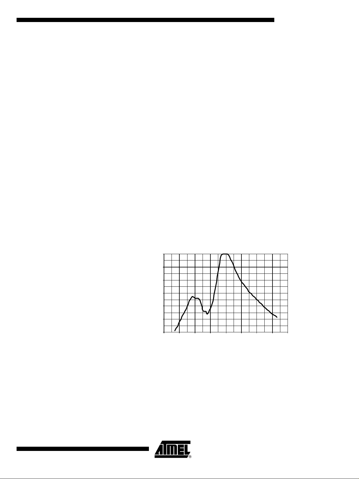
is illustrated in Figure 6 and Figu re 7. This exa mple relates to ASK m ode. FSK mode
exhibits a simila r beha vi or. T he pl ots are p ri nte d r ela tively to the maximu m sensitivity. If
a SAW filter is used, an i ns ertio n loss of about 3 dB must b e c onsidered, but the overall
selectivity is much better.
When designing the system in terms of receiving bandwidth, the LO deviation must be
considered as it al so determine s the IF center fre quency. The tot al LO deviatio n is
calculated, to be the sum of the deviat ion of the cry stal and the XT O deviatio n of the
T5760/T5761. Low-cost crystals are specified to be within ±90 ppm over tolerance,
temperature and aging. The XTO deviation of the T5760/T5761 is an additional
deviation due to the XTO circuit. This deviation is specified to be ±30 ppm worst case for
a crystal with CM = 7 fF. I f a cr y stal of ±90 ppm is used, the total deviation is ± 12 0 ppm
in that case. Note that the receiving bandwidth and the IF-filter bandwidth are equivalent
in ASK mode but not in FSK mode.
Figure 6. Narrow Band Receiving Frequency Response
0.0
-10.0
-20.0
4561B–RKE–10/02
-30.0
dP (dB)
-40.0
-50.0
-60.0
-4.0 -3.0 -2.0 -1.0 0.0 1.0 2.0 3.0 4.0
df (MHz)
7
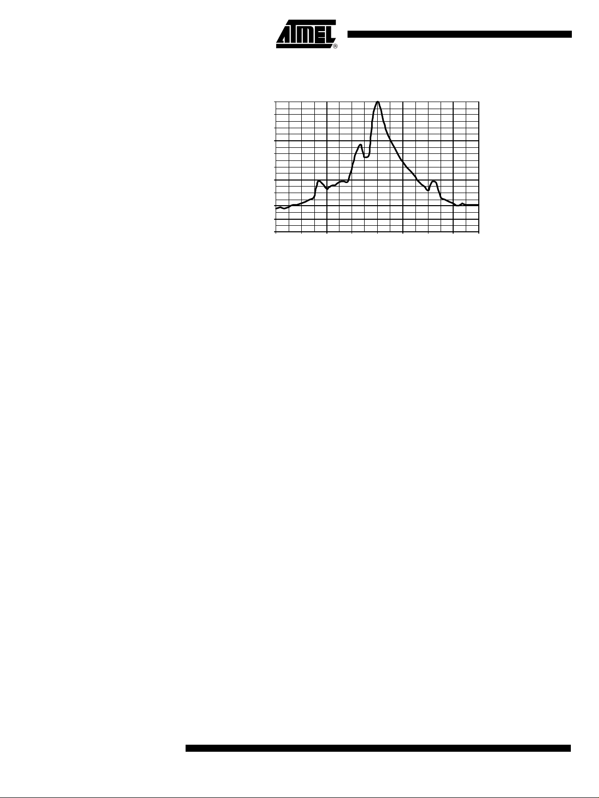
Figure 7. Wide Band Receiving Frequency Response
0.0
-10.0
-20.0
-30.0
-40.0
-50.0
-60.0
dP (dB)
-70.0
-80.0
-90.0
-100.0
-12.0 -9.0 -6.0 -3.0 0.0 3.0 6.0 9.0 12.0
df (MHz)
Polling Circuit and
Control Logic
Basic Clock Cycle of
the Digital Circuitry
The receiver is designed to consume less than 1 mA while being sensitive to signals
from a corresponding transmitter. This is achieved via the polling circuit. This circuit
enables the signal path per iodicall y for a short time. Dur ing this time the bit-check logic
verifies the presence of a valid transmitter signal. Only if a valid signal is detected, the
receiver remains ac tive and trans fers the d ata to the connec ted mi crocon troller . If there
is no valid signal pr es en t, th e r ecei ve r is in sl ee p mo de most of the time r esul ting in low
current consumpt ion . T hi s c ond iti on is c al led p oll in g m ode . A c on nec ted mi cro con tr oll er
is disabled during that time.
All relevant parameters of the polling logic can be configured by the connected microcontroller. This flexibility enables the user to meet the specifications in terms of current
consumption, system response time, data rate etc.
Regarding the number of con nection wires to the microcontroll er, the receiver is ve ry
flexible. It can be eith er operated by a sin gle bi-direction al line to save port s to the
connected microcontroller or it can be operated by up to five uni-directional ports.
The complete timing of the digital circuitry and the analog filtering is derived from one
clock. This cloc k cycle T
is derived from the crystal osc illator (XTO) in com bination
Clk
with a divide by 14 circuit. According to chapter ‘RF Front End’, the frequency of the
crystal oscillator (f
operating frequency of the local oscillator (f
giving T
T
Clk
= 2.066 µs for fRF= 868.3 MHz and T
Clk
controls the following application-relevant parameters:
) is defined by the RF in put signa l (f
XTO
). The basic clock cycle i s T
LO
= 1.961 µs for f
Clk
) which also defines th e
RFin
= 915 MHz.
RF
Clk
= 14/f
XTO
• Timing of the polling circuit including bit check
• Timing of the analog and digital signal processing
• Timing of the register programming
• Frequency of the reset marker
• IF filter center frequency (f
Most application s a re dom in ated by two transmissio n fr eq uen ci es : f
mainly used in USA , f
T
-dependent param eters on this ele ctrica l charac teristi cs displ ay thr ee conditi ons for
Clk
Transmit
)
IF0
= 915 MHz is
Transmit
= 868.3 MHz in Europe. In order to e ase the usage of all
each parameter.
8
T5760/T5761
4561B–RKE–10/02

T5760/T5761
• Application USA (f
• Application Europe (f
• Other applications The electrical characteristic is given as a function of T
= 7.14063 MHz, T
XTO
= 6.77617 MHz, T
XTO
= 1.961 µs)
Clk
= 2.066 µs)
Clk
Clk
.
The clock cycle of some function blocks depends on the selected baud-rate range
(BR_Range) which is define d in the OPMODE reg ister. T his cloc k cycl e T
is defined
XClk
by the following formulas for further reference:
BR_Range = BR_Range0: T
BR_Range1: T
BR_Range2: T
BR_Range3: T
XClk
XClk
XClk
XClk
= 8 ´ T
= 4 ´ T
= 2 ´ T
= 1 ´ T
Clk
Clk
Clk
Clk
Polling Mode According to Figure 11, the receiver stays in polling mode in a continuous cycle of three
different modes. In sleep mode the signal processi ng circuitry is disabled for the time
period T
all signal processing circuits are enabled and settled. In the following bit-check mode,
the incoming data stream is analyzed bit by bit contra a valid transmitter signal. If no
valid signal is present, the receiver is set back to sleep mode after the period T
This period varies check by check as it is a statistical process. An average value for
T
Bit-check
consumption is I
The average curre nt co nsu mpt ion i n p o llin g mode is depende nt o n t he duty c y cle o f th e
active mode and can be calculated as:
while consuming low current of IS=I
Sleep
. During the start-up perio d, T
Soff
is given in the electrical characteristics. During T
=I
S
. The condition of the receiver is indicated on Pin IC_ACTIVE.
Son
Startup
and T
Bit-check
Startup
Bit-check
the current
,
.
I
I
Spoll
During T
SoffTSleepISon
--------------------------------------------------------------------------------------------------------------=
Sleep
T
SleepTStartupTBit-check
and T
Startup
tee the reception o f a tran sm itte d command the trans mi tte r must start the telegram wi th
an adequate preburst. The required length of the preburst depends on the polling
parameters T
(T
Start_microcontroller
(N
Bit-check
) to be tested.
, T
Sleep
). Thus, T
Startup
The following formula indicates how to calculate the preburst length.
T
Preburst
³ T
Sleep
+ T
Startup
Sleep Mode The length of period T
the extension factor XSleep (according to Table 8), and the basic clock cycle T
calculated to be:
T
= Sleep ´ X
Sleep
In US- and European applications, the maximum value of T
is set to 1. The time reso lution is about 2 ms in tha t case. The sleep time can be
extended to almost half a second by setting XSleep to 8. XSleep can be set to 8 by bit
XSleep
Std
to’1’.
According to Tabl e 7, the hi gh es t reg is ter va lue o f s le ep sets th e re ce iv er i nto a p er manent sleep condition. The receiver remains in that condition until another value for Sleep
is programmed into the O PMODE register. This function is desirable wher e several
devices share a single data line and may also be used for microcontroller polling – via
Pin POLLING/_ON, the receiver can be switched on and off.
Sleep
T
+()´+´
StartupTBit-check
++
the receiver i s no t sensi tive to a tra nsm itter s ignal . To gu aran-
, T
Bit-check
+ T
is defined by the 5-bit word Sleep of the OPMODE register,
Sleep
´ 1024 ´ T
and the start-up time of a connected mi crocontr oller
Bit-check
depends on the actual bit rate and the number of bits
+ T
Bit-check
Start_microcontroller
Clk
is about 60 ms if XSleep
Sleep
Clk
. It is
4561B–RKE–10/02
9
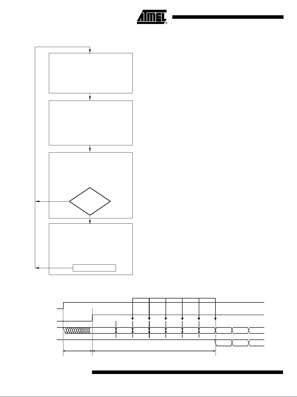
Figure 8. Polling Mode Flow Chart
Sleep mode:
All circuits for signal processing are
disabled. Only XTO and Polling logic is
enabled.
Output level on Pin IC_ACTIVE => low
I
= I
S
Soff
T
= Sleep x X
Sleep
Start-up mode:
The signal processing circuits are
enabled. After the start-up time (T
all circuits are in stable
condition and ready to receive.
Output level on Pin IC_ACTIVE => high
= I
I
S
Son
T
Startup
Bit-check mode:
The incomming data stream is
analyzed. If the timing indicates a valid
transmitter signal, the receiver is set to
receiving mode. Otherwise it is set to
Sleep mode.
Output level on Pin IC_ACTIVE => high
I
= I
S
Son
T
Bit-check
NO
Receiving mode:
The receiver is turned on permanently
and passes the data stream to the
connected microcontroller.
It can be set to Sleep mode through an
OFF command via Pin DATA or
POLLING/_ON.
Output level on Pin IC_ACTIVE => high
I
= I
S
Son
Sleep
Bit check
OK ?
OFF command
x 1024 x T
YES
Clk
Startup
Sleep: 5-bit word defined by Sleep0 to
Sleep4 in OPMODE register
X
: Extension factor defined by
Sleep
XSleepStd
according to Table 9
T
: Basic clock cycle defined by fXTO
Clk
)
T
Startup
and Pin MODE
: Is defined by the selected baud rate
range and TClk. The baud-rate range
is defined by Baud0 and Baud1 in
the OPMODE register.
T
: Depends on the result of the bit check
Bit-check
If the bit check is ok, T
depends on the number of bits to be
checked (N
utilized data rate.
Bit-check
) and on the
Bit-check
If the bit check fails, the average
time period for that check depends
on the selected baud-rate range and
on T
. The baud-rate range is
Clk
defined by Baud0 and Baud1 in the
OPMODE register.
Figure 9. Timing Diagram for Complete Successful Bit Check
( Number of checked Bits: 3 )
IC_ACTIVE
10
Bit check
Dem_out
Data_out (DATA)
T
Start-up
Start-up mode
T5760/T5761
1/2 Bit
1/2 Bit
T
Bit-check mode
Bit check ok
1/2 Bit 1/2 Bit 1/2 Bit 1/2 Bit
Bit-check
Receiving mode
4561B–RKE–10/02
T5760/T5761
Bit-check Mode In bit-check mode the incoming data str eam is examine d to distingu ish between a va lid
signal from a corresponding transmitter and signals due to noise. This is done by subsequent time frame checks where th e dis tances b etwe en 2 sig nal ed ges are continu ously
compared to a programmable time window. The maximum count of this edge-to-edge
tests before the receiver switches to receiving mode is also programmable.
Configuring the Bit
Check
Assuming a modulation scheme tha t contains 2 edges per bi t, two time fra me checks
are verifying one bit. This is valid for Manchester, Bi-phase and most other modulation
schemes. The maximum count of bits to be checked can be set to 0, 3, 6 or 9 bits via the
variable N
checks respectively. If N
in the OPMODE register. T his impli es 0, 6, 12 and 18 edge- to-edge
Bit-check
Bit-check
is set to a higher value, the receiv er is less likely to
switch to receiv ing mode due to noise. In the presenc e of a valid tr ansmit ter signal, the
bit check takes l e ss ti me if N
time is not dependent on N
Bit-check
is set to a lower value. In polling mode, the bit-check
Bit-check
. Figure 9 sho ws an exa mple w here 3 bits a re test ed
successfully and the data signal is transferred to Pin DATA.
According to Figure 10, the time window for the bit check is defined by two separate
time limits. If the edge-to-edge time t
the upper bit-check limit T
T
Lim_min
or tee exceeds T
Lim_max
Lim_max
is in between the lower bit-check limit T
ee
Lim_min
and
, the check will be continued. If tee is smaller than
, the bit check will be terminated and the receiver
switches to sleep mode.
Figure 10. Valid Time Window for Bit Check
1/f
Sig
t
Dem_out
T
Lim_min
T
Lim_max
ee
For best noise immunity it is recomme nded to use a low span between T
T
. This is achieved using a fixed frequency at a 50% duty cycle for the transmitter
Lim_max
Lim_min
and
preburst. A ‘11111...’ or a ‘10101...’ s equence in Manc hester or Bi-ph ase is a goo d
choice concerning that advice. A good compromise between receiver sensitivity and
susceptibility to noise is a time window of ± 30% regarding the expected edge-to-edge
time t
. Using pre-burst patterns that contain various edge-to-edge time periods, the bit-
ee
check limits must be programmed according to the required span.
The bit-check limits are determined by means of the formula below.
T
T
= Lim_min ´ T
Lim_min
= (Lim_max -1) ´ T
Lim_max
XClk
XClk
Lim_min and Lim_max are defined by a 5-bit word each within the LIMIT register.
Using above formulas, Lim_min and Lim_max can be determined according to the
required T
T
. The minimum edge-to-edge time tee (t
XClk
Lim_min
, T
Lim_max
and T
. The time resolution de fining T
XClk
DATA_L_min
, t
DATA_H_min
Lim_min
and T
Lim_max
is
) is defined according
to the chapter ‘Receiving Mode’. The lower limit should be set to Lim_min ³10. The maximum value of the upper limit is Lim_max = 63.
If the calculated value for Lim_min is <19, it is recommende d to check 6 or 9 bits
(N
) to prevent switching to receiving mode due to noise.
Bit-check
4561B–RKE–10/02
11

Figure 14, Figure 15 and Figure 16 illustrate the bit check for the bit-check li mits
Lim_min = 14 and Lim_max = 24. When the IC is enabled, the signal processing circuits
are enabled during T
fined during that period. Whe n the bit check becomes active, the bit-ch eck counter is
clocked with the cycle T
Figure 14 shows how the bit check proceeds i f the bit-check counter value CV_Lim is
within the limits defined by Lim_min and Lim_max at the occurrence of a signal edge. In
Figure 15 th e bi t ch ec k f ails as the valu e C V _L i m i s l ow e r t han t h e l im it L im _ mi n . T he bi t
check also fails if CV_Lim reaches Lim_max. This is illustrated in Figure 16.
Figure 11. Timing Diagram During Bit Check
. The output of the ASK/FSK demodulator (Dem_out) is unde-
Startup
.
XClk
( Lim_min = 14, Lim_max = 24 )
Bit check ok
IC_ACTIVE
Bit check
1/2 Bit
Dem_out
Bit-checkcounter
0
T
Start-up
Start-up mode
345
1
2
8
7
6 245
T
XClk
3 6789 111213
1
10
T
Bit-check
14
Bit-check mode
17 181234
15 16
Figure 12. Timing Diagram for Failed Bit Check (Condition: CV_Lim < Lim_min)
( Lim_min = 14, Lim_max = 24 )
IC_ACTIVE
Bit check
Dem_out
Bit-checkcounter
0
T
Start-up
Start-up mode
2345
1 1
6 245
36
T
Bit-check
Bit-check mode
Bit check failed ( CV_Lim < Lim_min )
1/2 Bit
789 111210
0
Sleep mode
T
Sleep
Bit check ok
1/2 Bit 1/2 Bit
56
78910111213
14 15
1234
Figure 13. Timing Diagram for Failed Bit Check (Condition: CV_Lim >= Lim_max)
12
( Lim_min = 14, Lim_max = 24 )
IC_ACTIVE
Bit check
Dem_out
Bit-checkcounter
0
T
Start-up
Start-up mode
T5760/T5761
23
45
1/2 Bit
6
2451
36
1
7
789 111210
T
Bit-check
13 14 15 161718 19 21 22 23 24
Bit-check mode
Bit check failed ( CV_Lim >= Lim_max )
20
0
T
Sleep
Sleep mode
4561B–RKE–10/02

T5760/T5761
Duration of the Bit Check If no transmitter signal is present during the bit check, the output of the ASK/FSK
demodulator deli ve rs random signals. The bit ch ec k is a sta t isti cal process and T
varies for each check. T herefor e, an aver age v alue for T
characteristics. T
baud-rate range causes a lo wer va lu e for T
depends on the selected baud-rate range and on T
Bit-check
resulting in a lower current consump-
Bit-check
is given in the electrical
Bit-check
tion in polling mode.
Bit-check
. A higher
Clk
In the presence of a valid transmitter signal, T
that signal, f
thereby results in a long er per io d for T
pre-burst T
, and the count of the checked bits, N
Sig
Bit-check
Preburst
.
requiring a higher val ue fo r the tr ans mitter
Receiving Mode If the bit check was successful for all bits specified by N
is dependent on the frequency of
Bit-check
. A higher value fo r N
Bit-check
, the receiver switches to
Bit-check
Bit-check
receiving mode. Acc ording to Figure 9, the internal data s ignal is switch ed to Pin
DATA in that case and the data clock is available after the start bit has been detected
(see Figure 20 ). A co nnected m icrocon trol ler c an b e wok en u p by the nega tive edge at
Pin DATA or by the data clock at Pin DATA_CLK. The receiver stays in that condition
until it is switched back to polling mode explicitly.
Digital Signal Processing The data from the AS K/FSK demodulator (Dem_out) is digitally processed in different
ways and as a result co nve rted i nto the o utput signal data. This proc es s ing depends on
the selected baud-rate range (BR_Ran ge). Figure 14 illustrates how Dem_out is synchronized by the extended clock cycle T
counter. Data can change its state on ly after T
period t
of the Data signal as a result is always an integral multiple of T
ee
The minimum time period between two edges of the data signal is limited to
t
ee
³ T
DATA_min
. This implies an efficient suppression of spikes at the DATA output. At the
same time it limits the maximum frequency of edges at DATA. This eases the interrupt
handling of a connected microcontroller.
The maximum time period for DATA to stay Low is limited to T
employed to ensu re a finite res ponse time in pro grammin g or switc hing off the recei ver
via Pin DATA. T
DATA_L_max
is thereby longer than the maxi mum tim e peri od indi cated by
the transmitter data stream. Figure 16 gives an example where Dem_out remains Low
after the receiver has switched to receiving mode.
. This clock is als o used for the bi t-check
XClk
has elapsed. The edg e-to- edge tim e
XClk
DATA_L_max
.
XClk
. This function is
Figure 14. Synchronization of the Demodulator Output
T
XClk
Clock bit-check
counter
Dem_out
Data_out (DATA)
4561B–RKE–10/02
t
ee
13
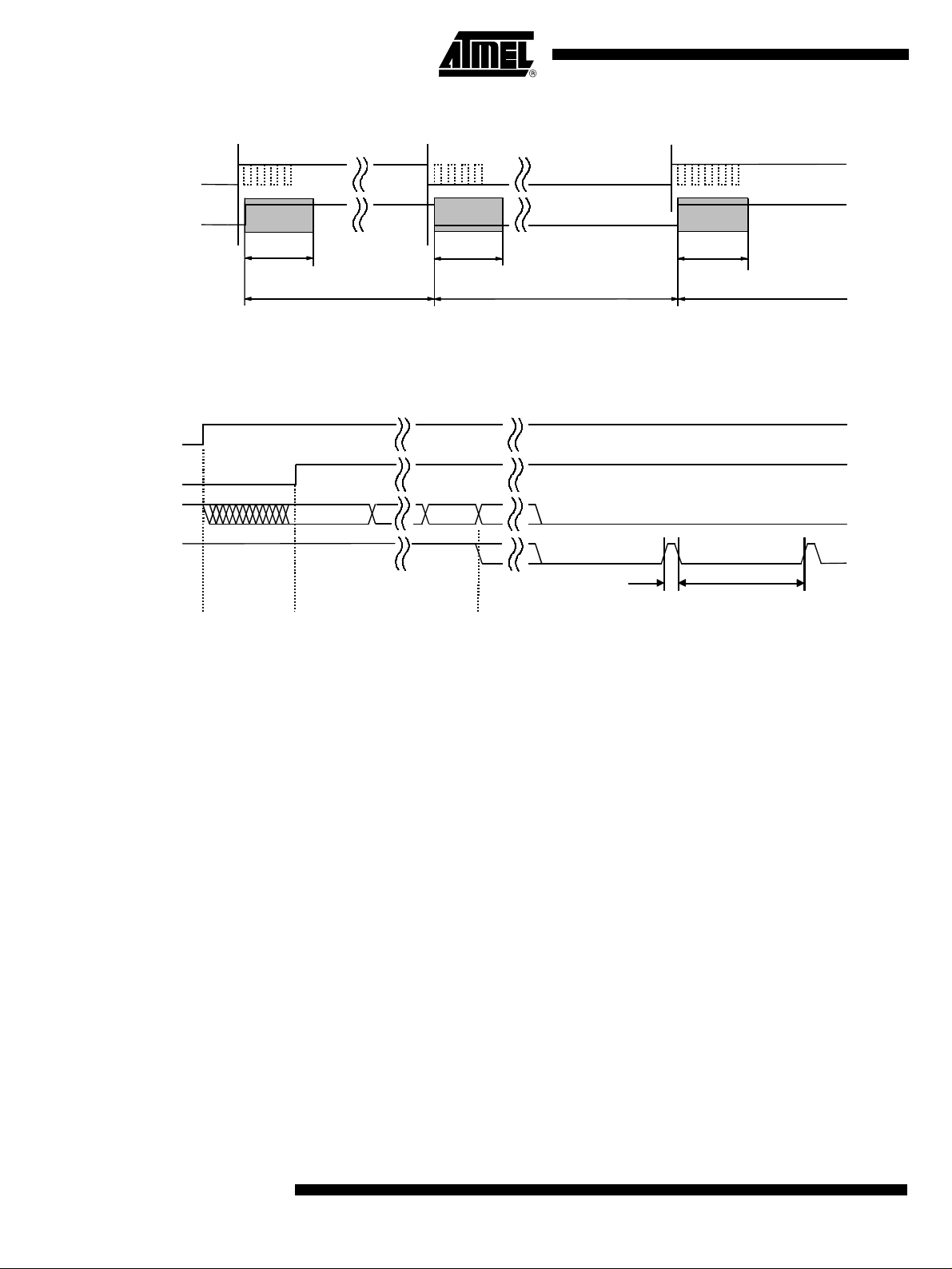
Figure 15. Debouncing of the Demodulator Output
Dem_out
Data_out (DATA)
t
DATA_min
t
ee
t
DATA_min
t
ee
Figure 16. Steady L State Limited DATA Output Pattern After Transmission
IC_ACTIVE
Bit check
Dem_out
t
DATA_min
t
ee
Data_out (DATA)
Start-up mode
Switching the Receiver
Back to Sleep Mode
t
DATA_L_max
Bit-check mode
Receiving mode
t
DATA_min
After the end of a data transmission, the receiver remains active. Depending of the bit
Noise_Disable in the OP MODE register, the output s ignal at Pin DATA is high or
random noise pulses appear at Pin DATA (see chapter ’Digital Noise Suppression’). The
edge-to-edge time period t
higher than T
DATA_min
.
of the majority of these noise pulses is equal or slightly
ee
The receiver can be set back to polling mode via Pin DATA or via Pin POLLING/_ON.
When using Pin DATA, this pin must be pulled to Low for the period t1 by the connected
microcontroller. Figure 17 illustrates the timing of the OFF command (see Figure 32).
The minimum value of t1 depends on BR_Range. The maximum value for t1 is not
limited but it is recommended not to exceed the specified value to prevent erasing the
reset marker. Note also that an internal reset for the OPMODE and the LIMIT register
will be generated if t1 exceeds the specified values. This item is explained in more detail
in the chapter ‘Configuration of the Receiver’. Setting the receiver to sleep mode via
DATA is achieved by prog ramming bit 1 to be ‘1’ d uring th e reg ister con figur ation. Only
one sync pulse (t3) is issued.
The duration of the OFF c ommand is determ ined by th e sum of t1, t2 and t10. Afte r the
OFF command the sl ee p ti me T
elapses. Note that the c apa ci tiv e loa d a t P in DATA
Sleep
is limited (see chapter ’Data Interface’).
14
T5760/T5761
4561B–RKE–10/02

Figure 17. Timing Diagram of the OFF Command via Pin DATA
T5760/T5761
IC_ACTIVE
Out1
(microcontroller)
Data_out (DATA)
Serial bi-directional
data line
t1 t2 t3
X
X
t4
Bit 1
("1")
t5
t10
t7
(Start bit)
OFF-command
Receiving
mode
Figure 18. Timing Diagram of the OFF Command via Pin POLLING/_ON
IC_ACTIVE
t
on2
t
on3
T
Sleep
Sleep mode
Bit check ok
T
Start-up
Start-up mode
POLLING/_ON
Data_out (DATA)
Serial bi-directional
data line
X
X
Receiving mode
Sleep mode Start-up mode Bit-check mode Receiving mode
Figure 19. Activating the Receiving Mode via Pin POLLING/_ON
IC_ACTIVE
t
on1
POLLING/_ON
Data_out (DATA)
Serial bi-directional
data line
Sleep mode Receiving mode
Start-up mode
X
X
X
X
4561B–RKE–10/02
15

Figure 18 illustrates how to set the receiver back to polling mode via Pin POLLING/_ON.
The Pin POLLING/_ON must be held to low for the time per iod t
edge on Pin POLLING /_ON and t he del ay t
time T
Sleep
elapses.
, the polling mode is ac tive and the sleep
on3
. After the positive
on2
This command is faster than using Pin DATA at the cost of an additional connection to
the microcontroller.
Figure 19 illustrates how to set the receiver to receiving mode via the Pin
POLLING/_ON. The Pin POLLING/_ON must be held to Low. After the delay t
on1
, the
receiver changes from s le ep mo de to sta rt -up mode regardless the p rogr amm ed v al ues
for T
and N
If the receiver is polled exclusively by a microcontroller, T
Sleep
Bit-check
and N
. As long as POLLING/_ON is held to L ow, the values for T
Bit-check
will be ignored, but not deleted (see chapter ’Digital Noise Suppression’).
must be programmed
Sleep
Sleep
to 31 (permanent sleep m ode). In this c ase the rec eiver r emai ns in s leep mode a s lon g
as POLLING/_ON is held to High.
Data Clock The Pin DATA_CLK makes a data shif t clo ck av ai lab le to sample the data stream into a
shift register. Using this data clo ck, a microcontrolle r can easily synchron ize the data
stream. This clock can only be used for Manchester and Bi-phase coded signals.
Generation of the Data
Clock
After a successfu l bit ch eck, the re ceiv er sw itche s from po llin g mode to rec eiving mod e
and the data stream i s ava ilable a t Pin DATA. In rece iving m ode, the dat a clock contro l
logic (Manchester/Bi-phase demodulator) is active and examines the incoming data
stream. This is done, like in the bit check, by subsequent time frame checks where the
distance between two edges is continuously compared to a programmable time window.
As illustrated in F igure 20, only two distances b etween tw o edges in M anchester a nd
Bi-phase coded signals are valid (T and 2T).
The limits for T are the same as us ed fo r the bi t che ck. T he y can be pr ogrammed in the
LIMIT-register (Lim_min and Lim_max, see Table 10 and Table 11).
The limits for 2T are calculated as follows:
Lower limit of 2T: Lim_min_2T = (Lim_min + Lim_max) - (Lim_max - Lim_min)/2
Upper limit of 2T: Lim_max_2T= (Lim_min + Lim_max) + (Lim_max - Lim_min)/2
(If the result for ’Lim_min_2T’ or ’Lim_max_2T’ is not an integer value, it will be round
up)
The data clock is available, after the data clock control logic has detected the
distance 2T (Start bit) and is issued with the delay t
after the edge on Pin DATA (see
Delay
Figure 20).
If the data clock control logic detects a ti ming or logical er ror (Manchester code viola-
tion), like illustrated in Figure 21 and Figure 22, it stops the output of the data clock. The
receiver remains in receiving mode and starts with the bit check. If the bit check was
successful and the start bit has been detected, the data clock control logic starts again
with the generation of the data clock (see Figure 23).
16
It is recommended to use the function of the data clock only in conjunction with the bit
check 3, 6 or 9. If the bit check is set to 0 or the receiver is set to receiving mode via the
Pin POLLING/_ON, the data clock is available if the data clock control logic has
detected the distance 2T (Start bit).
Note that for Bi-phase-coded signals, the data clock is issued at the end of the bit.
T5760/T5761
4561B–RKE–10/02

Figure 20. Timing Diagram of the Data Clock
Preburst Data
Bit check ok
T2T
'1' '1' '1' '1' '1' '0' '1' '1' '0' '1' '0'
Dem_out
Data_out (DATA)
DATA_CLK
Bit-check mode
Figure 21. Data Clock Disappears Because of a Timing Error
Timing error
'1' '1' '1' '1' '1' '0' '1' '1' '0' '1' '0'
(Tee < T
T
ee
Lim_min
OR T
Lim_max
Start bit
Data
<Tee< T
t
Delay
Receiving mode,
data clock control logic active
Lim_min_2T
OR Tee > T
Lim_max_2T
)
T5760/T5761
t
P_Data_Clk
Dem_out
Data_out (DATA)
DATA_CLK
Receiving mode,
data clock control
logic active
Figure 22. Data Clock Disappears Because of a Logical Error
'1' '1' '1' '0' '1' '1' '?' '0' '0' '1' '0'
Dem_out
Data_out (DATA)
DATA_CLK
Receiving mode,
data clock control
logic active
Receiving mode,
bit check active
Data
Logical error (Manchester code violation)
Receiving mode,
bit check aktive
4561B–RKE–10/02
17

Figure 23. Output of the Data Clock After a Successful Bit Check
Bit check ok
'1' '1' '1' '1' '1' '0' '1' '1' '0' '1' '0'
Dem_out
Data_out (DATA)
DATA_CLK
Receiving mode,
bit check active
Data
Start bit
Receiving mode,
data clock control
logic active
The delay of the data clock is calculated as follows: t
t
is the delay between the internal signals Data_Out and Data_In. For the rising
Delay1
edge, t
resistor R
depends on the cap acitive loa d CL at Pin DATA and the external pull-up
Delay1
. For the falling edge, t
pup
depends additionally on the external voltage V
Delay1
(see Figure 24, Figure 25 and Figure 32). When the level of Data_In is equal to the level
of Data_Out, the data clock is issued after an additional delay t
Note that the capacitive load at Pin DATA is limited. If the maximum tolerated capacitive
load at Pin DATA is exceeded, the data clock disappears (see chapter ’Data Interface’).
Figure 24. Timing Characteristic of the Data Clock (Rising Edge on Pin DATA)
Data_Out
Serial bi-directional
data line
Data_In
DATA_CLK
V
V
= 0,65 * V
Ih
= 0,35 * V
Il
V
X
S
S
t
t
Delay1
Delay2
t
t
P_Data_Clk
Delay
Figure 25. Timing Characteristic of the Data Clock (Falling Edge of the Pin DATA)
Delay
= t
Delay1
+ t
Delay2
Delay2
X
.
18
Data_Out
Serial bi-directional
data line
Data_In
DATA_CLK
T5760/T5761
t
Delay1
t
Delay
t
Delay2
t
P_Data_Clk
V
X
V
= 0,65 * V S
Ih
VIl = 0,35 * V S
4561B–RKE–10/02

T5760/T5761
Digital Noise
Suppression
Automatic Noise
Suppression
After a data transmiss ion, digital noise appears on the da ta output (see Figure 26). Preventing that digital no ise keeps the connec ted microcontroller busy . It can be
suppressed in two different ways.
If the bit Noise_Disable (Table 9) in the OPMODE register is set to 1 (default), the
receiver changes to bit-check mode at the end of a valid data stream. The digital noise
is suppressed and the level at Pin DATA is High in that case. The receiver changes
back to receiving mode, if the bit check was successful.
This way to suppress the noise is recommended if the data stream is Manchester or
Bi-phase coded and is active after power on.
Figure 28 illustrates the behavior of the data output at the end of a data stream. Note
that if the last period of the data stream is a high period (rising edge to falling edge), a
pulse occurs on Pin DATA . The len gth of the pulse d epends on the sele cted ba ud-rat e
range.
Figure 26. Output of Digital Noise at the End of the Data Stream
Bit check ok
Data_out (DATA)
DATA_CLK
Bit-check
mode
Preburst Data Digital Noise Preburst Data Digital NoiseDigital Noise
Receiving mode,
data clock control
logic active
Receiving mode,
bit check aktive
Bit check ok
Receiving mode,
data clock control
logic active
Receiving mode,
bit check aktive
Figure 27. Automatic Noise Suppression
Bit check ok Bit check ok
Data_out (DATA)
DATA_CLK
Bit-check
mode
Preburst Data Preburst Data
Receiving mode,
data clock control
logic active
Bit-check
mode
Figure 28. Occurrence of a Pulse at the End of the Data Stream
(tee < T
OR T
Lim_min
Timing error
Data stream Digital noise
'1' '1' '1'
Dem_out
Data_out (DATA)
DATA_CLK
data clock control
logic active
Lim_max
T
ee
< tee < T
T
Pulse
Lim_min_2T
Receiving mode,
data clock control
logic active
OR tee > T
Lim_max2T
Bit-check modeReceiving mode,
Bit-check
mode
4561B–RKE–10/02
19

Controlled Noise Suppression by the Micr ocontroller
Figure 29. Controlled Noise Suppression
Bit check ok Bit check ok
Serial bi-directional
data line
(DATA_CLK)
POLLING/_ON
Bit-check
mode
Configuration of the
Receiver
OFF-command
Preburst Data Digital Noise Preburst Data Digital Noise
Receiving mode
Start-up
mode
Bit-check
mode
Receiving mode
Sleep
mode
If the bit Noise_Disable (see Table 9) in the OPMODE register is set to 0, digital noise
appears at the end of a valid dat a stream. To suppress the noise, the Pi n
POLLING/_ON must be set to Low. The receiver remains in receiving mode. Then, the
OFF command causes the cha nge to the start-up mode. The programmed sleep tim e
(see Table 7) will not be executed beca use the level at P in POLLING/_ON is low, but
the bit check is active in that case. The OFF command activates the bit check also if the
Pin POLLING/_ON is held to Low. The receiver changes back to receiving mode if the
bit check was succ essf ul. To act ivate th e polling mode at the end of the da ta tran smission, the Pin POLLING/_ON must be set to High. This way of suppressing the noise is
recommended if the data stream is not Manchester or Bi-phase coded.
The T5760/T5761 receiver is configured via two 12-bit RAM registers called OPMODE
and LIMIT. The registers c an be programme d by means of the bid irectiona l DATA port.
If the register contents have changed due to a voltage drop, this condition is indicated by
a certain output pattern c alled reset marker (RM). T he receiver must be reprogr ammed
in that case. After a Power-On Reset (POR), the registers are set to default mode. If the
receiver is operated in defau lt mode , there is no need to program the regi sters. Ta ble 3
shows the structure o f th e r egi s ters. Ac c or din g to Tabl e 2 , bi t 1 def ines if the receiv er is
set back to polling mode via the OFF command (see chapter ’Receiving Mode’) or if it is
programmed. Bit 2 rep re se nts the regi ste r add ress . It se le cts th e ap pr opri ate re gi ste r to
be programmed. To get a high programming reliability, Bit 15 (Stop bit), at the end of the
programming operation, must be set to 0.
20
Table 1. Effect of Bit 1 and Bit 2 on Programming the Registers
Bit 1 Bit 2 Action
1 x The receiver is set back to polling mode (OFF command)
0 1 The OPMODE register is programmed
0 0 The LIMIT register is programmed
Table 2. Effect of Bit 15 on Programming the R egi ste r
Bit 15 Action
0 The values will be written into the register (OPMODE or LIMIT)
1 The values will not be written into the register
T5760/T5761
4561B–RKE–10/02

T5760/T5761
Table 3. Effect of the Configuration Words within the Registers
Bit 1 Bit 2 Bit 3 Bit 4 Bit 5 Bit 6 Bit 7 Bit 8 Bit 9 Bit 10 Bit 11 Bit 12 Bit 13 Bit 14 Bit 15
OFF command
1– – – – – – – – – – – – – –
– OPMODE register –
Noise
BR_Range N
01
Baud1 Baud0 BitChk1 BitChk0
Default
values of
Bit 3...14
– LIMIT register –
00
Default
values of
Bit 3...14
00 0 100011001–
Lim_
min5
01 0 101101001–
Lim_
min4
Bit-check
Lim_min Lim_max –
Lim_
min3
Lim_
min2
Modu-
lation
ASK/
_FSK
Lim_
min1
Sleep
Sleep4 Sleep3 Sleep2 Sleep1 Sleep0
Lim_
min0
Lim_
max5
Lim_
max4
Lim_
max3
Lim_
max2
X
Sleep
X
Sleep
Std
Lim_
max1
Suppres
sion
Noise_
Disable
Lim_
max0
0
0
The following tables illustrate the effect of the individual configuration words. The default
configuration is highlighted for each word.
BR_Range sets the appropr iate baud-r ate range and simulta neously defi nes XLim .
XLim is used to define the bit-check limits T
Lim_min
and T
as shown in Table 10 and
Lim_max
Table 11.
Table 4. Effect of the configurati on word BR_Ra nge
BR_Range
Baud-rate Range/Extension Factor for Bit-check Limits (XLim)Baud1 Baud0
BR_Range0
00
01
10
11
Table 5. Effect of the Configuration word N
00 0
0 1 3 (default)
10 6
11 9
(application USA/Europe: BR_Range0 = 1.0 kBaud to 1.8 kBaud)
XLim = 8 (default)
BR_Range1
(application USA/Europe: BR_Range1 = 1.8 kBaud to 3.2 kBaud)
XLim = 4
BR_Range2
(application USA/Europe: BR_Range2 = 3.2 kBaud to 5.6 kBaud)
XLim = 2
BR_Range3
(Application USA/Europe: BR_Range3 = 5.6 kBaud to 10 kBaud)
XLim = 1
Bit-check
N
Bit-check
Number of Bits to be CheckedBitChk1 BitChk0
4561B–RKE–10/02
21
Table 6. Effect of the Configuration Bit Modulation
Modulation Selected Modulation
ASK/_FSK –
0 FSK (default)
1 ASK
Table 7. Effect of the Configuration Word Sleep
Sleep
00000
00001
Start Value for Sleep Counter
= Sleep × Xsleep × 1024 × T
(T
Sleep
0 (Receiver is continuously polling until a
valid signal occurs)
1 (T
f
f
» 2.1 ms for XSleep = 1 and
Sleep
= 868.3 ms, » 2.0 ms for
RF
= 915 MHz)
RF
000102
000113
... ... ... ... ... ...
00110
6 (T
12.047 ms for f
= 12.695 ms for fRF = 868.3 MHz,
Sleep
RF
... ... ... ... ... ...
1110129
1111030
1 1 1 1 1 31 (permanent sleep mode)
Table 8. Effect of the Configuration Bit XSleep
XSleep
XSleep
Std
01 (default)
18
Extension Factor for Sleep Time
(TSleep = Sleep × Xsleep × 1024 × T
Clk
= 915 MHz) (default)
Clk)
)Sleep4 Sleep3 Sleep2 Sleep1 Sleep0
22
Table 9. Effect of the Configuration Bit Noise Suppression
Noise Suppression
Suppression of the Digital Noise at Pin DATANoise_Disable
0 Noise suppression is inactive
1 Noise suppression is active (default)
T5760/T5761
4561B–RKE–10/02

T5760/T5761
Table 10. Effect of the Configuration Word Lim_min
Lim_min
Lim_min5 Lim_min4 Lim_min3 Lim_min2 Lim_min1 Lim_min0 (T
001010 10
001011 11
001100 12
.. .. .. .. .. ..
010101
.. .. .. .. .. ..
111101 61
111110 62
111111 63
Note: 1. Lim_min is also used to determine the margins of the data clock control logic (see chapter ’Data Clock’).
(1)
(Lim_min < 10 is not Applicable) Lower Limit Value for Bit Check
= Lim_min × XLim × T
Lim_min
21 (default)
(T
= 347 µs for fRF = 868.3 MHz and
Lim_min
BR_Range0
T
= 329 µs for fRF = 915 MHz and
Lim_min
BR_Range0)
Clk
)
Table 11. Effect of the Configuration Word Lim_max
Lim_max
Lim_max5 Lim_max4 Lim_max3 Lim_max2 Lim_max1 Lim_max0
001100 12
001101 13
001110 14
.. .. .. .. .. ..
101001
.. .. .. .. .. ..
111101 61
111110 62
111111 63
Note: 1. Lim_max is also used to determine the margins o f the data clock control logic (see chapt er ’Data Clock’).
(1)
(Lim_max < 12 is not applicable) Upper Limit Value for Bit Check
(TLim_max = (Lim_max - 1) × XLim ×
T
)
Clk
41 (defaul t)
(TLim_max = 661 µs for f
and BR_Range0, TLim_max = 627 µs for
fRF = 915 MHz and BR_Range0)
= 868.3 MHz
RF
4561B–RKE–10/02
23

Conservation of the
Register Information
The T5760/T 5761 implies an integrate d power-on rese t and brown-o ut detection
circuitry to provide a mechanism to preserve the RAM register information.
According to Figure 30, a power-on reset (POR) is gen erated if the supply vo ltage V
drops below the threshold voltage V
the configuration registers in that condition. Once V
canceled after the minimum reset per iod t
voltage of the receiver is turned on.
To indicate that condition, the receiver displays a reset marker (RM) at Pin DATA after a
reset. The RM is represented by the fixed frequency f
canceled via a Low pulse t1 at Pin DATA. The RM implies the following characteristics:
•f
is lower than the lowest feasible frequency of a data signal. By this means, RM
RM
cannot be misinterpreted by the connected microcontroller.
• If the receiver is set back to polling mode via Pin DATA, RM cannot be canceled by
accident if t1 is applied according to the proposal in the section “Programming the
Configuration Registers”.
By means of t hat mechan ism the receiv er cannot lose i ts regis ter infor mation without
communicating that condition via the reset marker RM.
Figure 30. Generation of the Power-on Reset
V
S
POR
t
Rst
Data_out (DATA)
X
V
ThReset
. The default parameters are programmed into
ThReset
. A POR is also ge ner at ed when th e s up ply
Rst
exceeds V
S
at a 50% duty-cyc le. RM can be
RM
1 / f
RM
ThReset
S
the POR is
24
T5760/T5761
4561B–RKE–10/02

Programming the Configuration Register
Figure 31. Timing of the Register Programming
IC_ACTIVE
t1 t2 t3t4t5
t6
Out1
(microcontroller)
t7
T5760/T5761
t9
t8
Data_out (DATA)
Serial bi-directional
data line
X
X
Receiving
mode
Figure 32. Data Interface
VS= 4.5 V to 5.5 V
Data_In
Data_out
Input Interface
(Start bit)
T5760/
T5761
Bit 1
("0")
0 ... 20 V0 V / 5 V
Bit 2
("1")
(Register select)
Programming frame
DATA
I
D
Bit 14
("0")
(Poll8) (Stop bit)
VX= 5 V to 20 V
R
pup
Serial bi-directional data line
C
L
I/O
Bit 15
("0")
Microcontroller
Out1 (microcontroller )
T
SleepTStart-up
Start-up
Sleep
mode
mode
4561B–RKE–10/02
The configuration registers are programmed serially via the bi-directional data line
according to Figure 31 and Figure 32.
To start programming, the serial data line DATA is pulled to Low for the time period t1 by
the microcontroller. When DATA has been released, the receiver becomes the master
device. When the programming delay period t2 has elapsed, it emits 15 subsequent
synchronization pulses with the pulse length t3. After each of these pulses, a programming window occurs. The delay until the program window starts is determined by t4, the
duration is defined by t5. Within the programming window, the individual bits are set. If
the microcon trolle r pulls down P in DATA f or the ti me per iod t7 du ring t5 , the acco rdin g
bit is set to ’0’. If no programming pulse t7 is issued, this bit is set to ’1’. All 15 bits are
subsequently programmed this way. The time frame to program a bit is defined by t6.
25

Bit 15 is followed by the equivalent time window t9. During this window, the equivalence
acknowledge pulse t8 (E_Ack) occurs if the just programmed mode word is equivalent to
the mode word that was already stored in that register. E_Ack should be used to verify
that the mode word was correctly transferred to the register. The register must be programmed twice in that case.
Programming of a register is possible both in sleep-mode and in active-mode of the
receiver.
During programming, the LNA, LO, lowpass filter IF- amplifier and the FSK/A SK
Manchester demodulat or are disabled.
The programming start pulse t1 initi ates the pr ogrammi ng of the config uration re gisters .
If bit 1 is set to ’1’, it represents th e OFF command to set the r eceiver bac k to polli ng
mode at the same time. For the length of the programming start pulse t1, the following
convention should be considered:
• t1(min) < t1 < 5632 T
Clk
:
t1(min) is the minimum specified value for the relevant BR_Range
Programming respectively OFF command is initiated if the receiver is not in reset mode.
If the receiver is in reset mode, programming respectively Off command is not initiated
and the reset marker RM is still present at Pin DATA.
This period is generally used to switch the receiver to polling m ode or to start the
programming of a register. In reset condition, RM is not cancelled by accident.
• t1 > 7936 x T
Clk
Programming respectively OFF command is in itiated in any case. The registers
OPMODE and LIMIT are set to the default values. RM is cancelled if present.
This period is used if the connected microcontroller detected RM. If the receiver operates in default mode, this time period for t1 can generally be used.
Note that the capacitive load at Pin DATA is limited.
Data Interface The data interface (see Figure 32) is desig ned for automotive requirements. It c an be
connected via the pull-up resistor R
The applicable pull-up resistor R
the selected BR_range (see Table 12).
Table 12. Applicable R
- BR_range Applicable R
CL £ 1nF
CL £ 100pF
pup
up to 20 V and is short-circuit-protected.
pup
depends on the load capacity CL at Pin DATA and
pup
pup
B0 1.6 k
B1 1.6 kW to 22 kW
B2 1.6 kW to 12 kW
B3 1.6 kW to 5.6 kW
B0 1.6 k
B1 1.6 kW to 220 kW
B2 1.6 kW to 120 kW
B3 1.6 kW to 56 kW
W to 47 kW
W to 470 kW
26
T5760/T5761
4561B–RKE–10/02

Figure 33. Application Circuit: fRF = 868.3 MHz without SAW Filter
VS
GND
C7
4.7u
10%
C14
C13
10n
10%
39n 5%
1
2
3
4
5
6
7
8
9
10
SENS
IC_ACTIVE
CDEM
AVCC
TEST1
AGND
n.c.
LNAREF
LNA_IN
LNAGND
R2
56k to 150k
POLLING/_ON
DATA_CLK
T5760/
T5761
DATA
DGND
TEST4
DVCC
XTAL
n.c.
TEST3
TEST2
20
19
18
17
16
15
14
13
12
11
Q1
6.77617 MHz
C12
10n
10%
C11
12p
2%
R3
>= 1.6k
np0
T5760/T5761
IC_ACTIVE
Sensitivity reduction
VX = 5 V to 20 V
DATA
POLLING/_ON
DATA_CLK
RF_IN
C17
1.5p
±0.1p
np0
Figure 34. Application Circuit: f
VS
C7
4.7u
10%
GND
RF_IN
Toko LL1608-FS12NJ
12nH, 5%
C2
3.3p
±0.1p
np0
1
2
3
4
C16
18p
5%
np0
Toko LL1608-FS4N7S
4.7nH, ±0.3nH
= 868.3 MHz with SAW Filter
RF
R2
56k to 150k
1
C14
C13
10n
10%
EPCOS B3570
IN
IN_GND
CASE_GND
CASE_GND
39n 5%
2
3
4
5
6
7
8
9
10
C16
18p
5%
np0
OUT
OUT_GND
CASE_GND
CASE_GND
4.7nH, ±0.3nH
SENS
IC_ACTIVE
CDEM
AVCC
TEST1
AGND
n.c.
LNAREF
LNA_IN
LNAGND
POLLING/_ON
T5760/
T5761
C17
5.6p
±0.1p
np0
Toko LL1608-FS4N7S
5
6
7
8
DATA
DGND
DATA_CLK
TEST4
DVCC
XTAL
TEST3
TEST2
n.c.
20
19
18
17
16
15
14
13
12
11
Q1
6.77617 MHz
C12
10n
10%
C11
12p
2%
R3
>= 1.6k
np0
IC_ACTIVE
Sensitivity reduction
VX = 5 V to 20 V
DATA
POLLING/_ON
DATA_CLK
4561B–RKE–10/02
27

Absolute Maximum Ratings
Parameters Symbol Min. Max. Unit
Supply voltage V
Power dissipation P
Junction tem p erature T
Storage temperature T
Ambient temperature T
Maximum input level, input matched to 50
W P
in_max
S
tot
stg
amb
j
-55 +125 °C
-40 +105 °C
6V
1000 mW
150 °C
10 dBm
Thermal Resistance
Parameters Symbol Value Unit
Junction ambient R
thJA
100 K/W
Electrical Characteristics
All paramete rs refer to G ND, T
= -40°C to +105°C, VS = 4.5 V to 5.5 V, f0 = 868.3 MHz and f0=915MHz,
amb
unless otherwise specified. (For typical values: V
f
= 868.3 MHz
RF
6.77617 MHz Oscillator
Parameter Test Conditions Symbol
Basic Clock Cycle of the Digital Circuitry
Basic clock
cycle
Extended
basic clock
cycle
Polling Mode
Sleep time
(see
Figure 11,
Figure 20 and
Figure 33)
Start-up time
(see
Figure 11 and
Figure 12)
Time for bit
check (see
Figure 11)
BR_Range0
BR_Range1
BR_Range2
BR_Range3
Sleep and XSleep
are defined in the
OPMODE register T
BR_Range0
BR_Range1
BR_Range2
BR_Range3
Average bit-check
time while polling,
no RF applied
(see Figure 15 and
Figure 16)
BR_Range0
BR_Range1
BR_Range2
BR_Range3
T
T
Clk
T
XClk
Sleep
T
Startup
Bit-check
2.0662 2.0662 1.9607 1.9607 14/f
16.53
8.26
4.13
2.07
Sleep ´
X
´
Sleep
1024 ´
2.0662
1852
1059
1059
662
= 5 V, T
S
0.45
0.24
0.14
0.08
16.53
8.26
4.13
2.07
Sleep ´
X
´
Sleep
1024 ´
2.0662
1852
1059
1059
662
= 25°C)
amb
fRF = 915 MHz
7.14063 MHz Oscillator Variable Oscillator
XTO
15.69
7.84
3.92
1.96
Sleep ´
X
Sleep
1024 ´
1.9607
1758
1049
1049
628
´
0.45
0.24
0.14
0.08
15.69
7.84
3.92
1.96
Sleep ´
X
´
Sleep
1024 ´
1.9607
1758
1049
1049
628
8 ´ T
4 ´ T
2 ´ T
1 ´ T
Sleep ´
X
Sleep
1024 ´ T
896.5
512.5
512.5
320.5
´ T
Clk
Clk
Clk
Clk
Clk
´
Clk
14/f
XTO
8 ´ T
4 ´ T
2 ´ T
1 ´ T
Sleep ´
X
Sleep
1024 ´ T
896.5
512.5
512.5
320.5
´ T
Clk
UnitMin. Typ. Max. Min. Typ. Max. Min. Typ. Max.
µs
µs
Clk
µs
Clk
µs
Clk
µs
Clk
´
ms
Clk
µs
µs
µs
µs
µs
ms
ms
ms
ms
28
T5760/T5761
4561B–RKE–10/02

Electrical Characteristics (Continued)
T5760/T5761
All paramete rs refer to G ND, T
= -40°C to +105°C, VS = 4.5 V to 5.5 V, f0 = 868.3 MHz and f0=915MHz,
amb
unless otherwise specified. (For typical values: V
f
= 868.3 MHz
RF
6.77617 MHz Oscillator
Parameter Test Conditions Symbol
Time for bit
check (see
Figure 11)
Receiving Mode
Intermediate
frequency
Baud-rate
range
Minimum time
period
between edges
at Pin DATA
(see
Figure 18 and
Figure 19)
(With the
exception of
parameter
T
)
Pulse
Maximum Low
period at Pin
DATA
(see
Figure 16)
Dela y to
activate the
start-up mode
(see
Figure 22)
OFF command
at Pin
POLLING/_ON
(see
Figure 21)
Dela y to
activate the
sleep mode
(see
Figure 21)
Pulse on Pin
DATA at the
end of a data
stream
(see
Figure 30)
Bit-check time for
a valid input signal
(see Figure 12)
f
Sig
N
= 0
Bit-check
N
= 3
Bit-check
= 6
N
Bit-check
N
= 9
Bit-check
BR_Range0
BR_Range1
BR_Range2
BR_Range3
BR_Range =
BR_Range0
BR_Range1
BR_Range2
BR_Range3 t
BR_Range =
BR_Range0
BR_Range1
BR_Range2
BR_Range3
BR_Range =
BR_Range0
BR_Range1
BR_Range2
BR_Range3
T
Bit-check
3/f
Sig
6/f
Sig
9/f
Sig
f
IF
1.0
BR_Range
1.8
3.2
5.6
165.3
82.6
41.3
DATA_min
20.7
2149
t
DATA_L_max
1074
537
269
Ton1 19.6 21.7 18.6 20.6 9.5 ´ T
Ton2 16.5 15.6 8 ´ T
Ton3 17.6 19.6 16.6 18.6 8.5 ´ T
16.5
T
Pulse
8.3
4.1
2.1
= 5 V, T
S
= 25°C)
amb
fRF = 915 MHz
7.14063 MHz Oscillator Variable Oscillator
UnitMin. Typ. Max. Min. Typ. Max. Min. Typ. Max.
3.5/f
6.5/f
9.5/f
1 ´ T
3/f
Sig
Sig
Sig
Sig
6/f
Sig
9/f
Sig
3.5/f
6.5/f
9.5/f
Sig
Sig
Sig
XClk
3/f
Sig
6/f
Sig
9/f
Sig
1 ´ T
3.5/f
6.5/f
9.5/f
ms
Clk
Sig
Sig
Sig
ms
ms
ms
0.95 1.00 fRF/915 MHz
1.8
3.2
5.6
10.0
165.3
82.6
41.3
20.7
2149
1074
537
269
16.5
8.3
4.1
2.1
1.054
1.89
3.38
5.9
156.8
78.4
39.2
19.6
2139
1020
510
255
15.69
7.84
3.92
1.96
1.89
3.38
5.9
10.5
156.8
78.4
39.2
19.6
2139
1020
510
255
15.69
7.84
3.92
1.96
BR_Range0 ´ 2 µs/T
BR_Range1 ´ 2 µs/T
BR_Range2 ´ 2 µs/T
BR_Range3 ´ 2 µs/T
10 ´ T
XClk
10 ´ T
XClk
10 ´ T
XClk
10 ´ T
XClk
130 ´ T
XClk
130 ´ T
XClk
130 ´ T
XClk
130 ´ T
XClk
Clk
Clk
Clk
8 ´ T
Clk
4 ´ T
Clk
2 ´ T
Clk
1 ´ T
Clk
Clk
Clk
Clk
Clk
10 ´ T
10 ´ T
10 ´ T
10 ´ T
130 ´ T
130 ´ T
130 ´ T
130 ´ T
10.5 ´ T
9.5 ´ T
8 ´ T
4 ´ T
2 ´ T
1 ´ T
XClk
XClk
XClk
XClk
Clk
Clk
Clk
Clk
XClk
XClk
XClk
XClk
Clk
Clk
kBaud
kBaud
kBaud
kBaud
µs
µs
µs
µs
µs
µs
µs
µs
µs
µs
µs
µs
µs
µs
µs
4561B–RKE–10/02
29

Electrical Characteristics (Continued)
All paramete rs refer to G ND, T
= -40°C to +105°C, VS = 4.5 V to 5.5 V, f0 = 868.3 MHz and f0=915MHz,
amb
unless otherwise specified. (For typical values: V
f
= 868.3 MHz
RF
6.77617 MHz Oscillator
Parameter Test Conditions Symbol
Configuration of the Receiver (see Figure 17 and Figure 33)
Frequency of
the reset
marker
Programming
start pulse
Programming
delay period
Synchronization pulse
Delay until of
the program
window starts
Programming
window
Time frame
of a bit
Programming
pulse
Equivalent
acknowledge
pulse: E_Ack
Equivalent
time window
OFF-bit
programming
window
Data Clock (see Figure 27 and Figure 28)
Minimum delay
time between
edge at DATA
and
DATA_CLK
Pulse width of
negative pulse
at Pin
DATA_CLK
Frequency is
stable within
50 ms after POR
BR_Range =
BR_Range0
BR_Range1
BR_Range2
BR_Range3
after POR
BR_Range =
BR_Range0
BR_Range1
BR_Range2
BR_Range3
BR_Range =
BR_Range0
BR_Range1
BR_Range2
BR_Range3
f
RM
118. 2 118.2 124.5 124.5
3355
t1
2273
1731
1461
16397
t2 795 797 754 756 384.5 ´ T
t3 264 264 251 251 128 ´ T
t4 131 131 125 125 63.5 ´ T
t5 529 529 502 502 256 ´ T
t6 1058 1058 1004 1004 512 ´ T
t7 132 529 125 502 64 ´ T
t8 264 264 251 251 128 ´ T
t9 533 533 506 506 258 ´ T
t10 929 929 881 881 449.5 ´ T
0
t
Delay2
0
0
0
66.1
t
P_DATA_CLK
33.0
16.5
8.3
= 5 V, T
S
11637
11637
11637
11637
16.5
8.3
4.1
2.1
66.1
33.0
16.5
8.3
= 25°C)
amb
fRF = 915 MHz
7.14063 MHz Oscillator Variable Oscillator
1/
3184
2168
1643
1386
15560
0
0
0
0
63
31
15.7
7.8
(4096 ´ T
11043
11043
11043
11043
16.7
7.8
3.9
1.96
63
31
15.7
7.8
1624 ´ T
1100 ´ T
838 ´ T
707 ´ T
7936 ´ T
0
0
0
0
4 ´ T
4 ´ T
4 ´ T
4 ´ T
Clk
Clk
Clk
Clk
Clk
Clk
Clk
Clk
Clk
Clk
Clk
Clk
Clk
Clk
Clk
XClk
XClk
XClk
XClk
UnitMin. Typ. Max. Min. Typ. Max. Min. Typ. Max.
)
(4096 ´ T
5632 ´ T
5632 ´ T
5632 ´ T
5632 ´ T
1/
Hz
)
Clk
µs
Clk
µs
Clk
µs
Clk
µs
Clk
µs
385.5 ´ T
128 ´ T
63.5 ´ T
256 ´ T
512 ´ T
256 ´ T
128 ´ T
258 ´ T
449.5 ´ T
1 ´ T
XClk
1 ´ T
XClk
1 ´ T
XClk
1 ´ T
XClk
4 ´ T
XClk
4 ´ T
XClk
4 ´ T
XClk
4 ´ T
XClk
µs
Clk
µs
Clk
µs
Clk
µs
Clk
µs
Clk
µs
Clk
µs
Clk
µs
Clk
µs
Clk
µs
µs
µs
µs
µs
µs
µs
µs
30
T5760/T5761
4561B–RKE–10/02
Electrical Characteristics (continued)
T5760/T5761
All paramete rs refer to G ND, T
unless otherwise specified. (For typical values: V
= -40°C to +105°C, VS = 4.5 V to 5.5 V, f0 = 868.3 MHz and f0=915MHz,
amb
= 5 V, T
S
= 25°C)
amb
Parameters Test Conditions Symbol Min. Typ. Max. Unit
Current consumption Sleep mode
(XTO and polling logic activ e)
IS
off
170 276 µA
IC active (start-up-, bit-check-,
receiving mode) Pin DATA = H
FSK
ASK
IS
on
7.8
7.4
9.9
9.6
LNA, Mixer, Polyphase Lowpass and IF Amplifier (Input Matched According to Figure 33 Referred to RFIN)
Third-order intercept point LNA/mixer/IF amplifier IIP3 -16 dBm
LO spurious emission Required according to I-ETS 300220 IS
LORF
-70 -57 dBm
System noise figure With power matching |S 11| < -10 dB NF 5 dB
LNA_IN input impedance at 868.3 MHz
at 915 MHz
Zi
1 dB compression point IP
LNA_IN
1db
200 || 3.2
200 || 3.2
-25 dBm
W || pF
W || pF
Image rejection Within the complete image band 20 3 0 dB
Maximum input level BER
FSK mode
ASK mode
£ 10
-3
,
P
in_max
-10
-10
dBm
dBm
Local Oscillator
Operating frequency range VCO T5760
T5761
Phase noise local oscillator f
Spurious of the VCO at ±f
= 867.3 MHz at 10 MHz L (fm) -140 -130 dBC/Hz
osc
XTO
f
VCO
f
VCO
866
900
871
929
MHz
MHz
-55 -45 dBC
XTO pulling XTO pulling,
appropriate load capacitance must
be connected to XTAL,
Series resonance resistor of the
crystal
Static capacitance at Pin XTAL to
GND
crystal C
f
XTAL
f
XTAL
Parameter of the supplied crystal
Parameter of the supplied crystal
and board parasitics
= 7 fF
M
= 6.77617 MHz (EU)
= 7.14063 MHz (US)
f
XTO
R
C
-30ppm f
S
0
XTAL
+30ppm MHz
120 W
6.5 pF
Analog Signal Processing (Input Matched According to Figure 33 Referred to RFIN)
Input sensitivity ASK ASK (level of carrier)
BER
= 868.3 MHz/915 MHz
f
in
V
S
= 950 kHz/1 MHz
f
IF
BR_Range0 -110 -112 -114 dBm
£ 10
= 5 V, T
-3
, 100% Mod
= 25°C
amb
P
Ref_ASK
BR_Range1 -108.5 -110.5 -112.5 dBm
BR_Range2 -108 -110 -112 dBm
BR_Range3 -106 -108 -110 dBm
mA
mA
4561B–RKE–10/02
31

Electrical Characteristics (continued)
All paramete rs refer to G ND, T
unless otherwise specified. (For typical values: V
= -40°C to +105°C, VS = 4.5 V to 5.5 V, f0 = 868.3 MHz and f0=915MHz,
amb
= 5 V, T
S
= 25°C)
amb
Parameters Test Conditions Symbol Min. Typ. Max. Unit
Sensitivity variation ASK for the full
operating range compared to
= 25°C, VS=5V
T
amb
Sensitivity variation ASK for full
operating range including IF filter
compared to T
=25°C, VS = 5 V
amb
Input sensitivity FSK BER
f
= 868.3 MHz/915 MHz
in
= 950 kHz/1 MHz
f
IF
= P
P
ASK
= 868.3 MHz/915 MHz
f
in
f
= 950 kHz/1 MHz
IF
-210 kHz to +210kHz
f
IF
-270 kHz to +270kHz
f
IF
P
= P
ASK
£ 10
Ref_ASK
Ref_ASK
-3
+ DP
+ DP
Ref
Ref
DP
DP
Ref
Ref
+2.5 -1.0 dB
+5.5
+7.5
-1.5
-1.5
fin = 868.3 MHz/915 MHz
= 5 V, T
V
S
f
= 950 kHz/1 MHz
IF
amb
= 25°C
BR_Range0
df = ±16 kHz to ±28kHz
df = ±10 kHz to ±100 kHz
P
Ref_FSK
-103
-101
-106 -107.5
-107.5
dBm
dBm
BR_Range1
df = ±16 kHz to ±28kHz
df = ±10 kHz to ±100 kHz
P
Ref_FSK
-101
-99
-104 -105.5
-105.5
dBm
dBm
BR_Range2
df = ±18 kHz to ±31kHz
df = ±13 kHz to ±100 kHz
P
Ref_FSK
-99.5
-97.5
-102.5 -104 dBm
dBm
BR_Range3
Sensitivity variation FSK for the full
operating range compared to
= 25°C, VS = 5 V
T
amb
Sensitivity variation FSK for the full
operating range including IF filter
compared to
T
amb
= 25°C,
VS = 5 V
S/N ratio to suppress inband noise
signals. Noise signa ls ma y ha ve
df = ±25 kHz to ±44kHz
df = ±20 kHz to ±100 kHz
fin = 868.3 MHz/915 MHz
= 950 kHz/1 MHz
f
IF
P
FSK
= P
Ref_FSK
+ DP
Ref
fin = 868.3 MHz/915 MHz
= 950 kHz/1 MHz
f
IF
-150 kHz to +150kHz
f
IF
f
-200 kHz to +200kHz
IF
-260 kHz to +260kHz
f
IF
= P
P
FSK
Ref_FSK
+ DP
Ref
ASK mode
FSK mode
P
Ref_FSK
DP
DP
SNR
SNR
Ref
Ref
ASK
FSK
-97.5
-100.5 -102 dBm
-95.5
+3 -1.5 dB
+6
+8
+11
10
2
-2
-2
-2
12
3
dBm
any modulation scheme
Dynamic range RSSI amplifier DR
Lower cut-off frequen cy of the data
filter
f
cu_DF
------------ ------------- ------------- ----------- ----------=
2
1
p´ 30 kW´ CDEM´
fcu_DF 0.11 0.16 0.20 kHz
RSSI
60 dB
CDEM = 33 nF
Recommended CDEM for best
performance
BR_Range0 (default)
BR_Range1
BR_Range2
BR_Range3
CDEM
39
22
12
8.2
dB
dB
dB
dB
dB
dB
dB
nF
nF
nF
nF
32
T5760/T5761
4561B–RKE–10/02

Electrical Characteristics (continued)
T5760/T5761
All paramete rs refer to G ND, T
unless otherwise specified. (For typical values: V
= -40°C to +105°C, VS = 4.5 V to 5.5 V, f0 = 868.3 MHz and f0=915MHz,
amb
= 5 V, T
S
= 25°C)
amb
Parameters Test Conditions Symbol Min. Typ. Max. Unit
Edge-to-edge time period of the
input data signal for full sensitivity
BR_Range0 (default)
BR_Range1
BR_Range2
BR_Range3
t
ee_sig
270
156
89
50
1000
560
320
180
Upper cut-off frequency data filter Upper cut-off frequency
programmable in 4 ranges
via a serial mode word
BR_Range0 (default)
BR_Range1
BR_Range2
BR_Range3
Reduced sensitivity R
connected from PinSens
Sense
, input matched according to
to V
S
Figure 33,
Reduced sensitivity variati on ov er
full operating range
Reduced sensitivity variati on for
different values of R
Sense
fIN = 868.3 MHz/915 MHz, V
= +25°C
T
amb
R
= 56 kW P
Sense
R
= 100 kW P
Sense
R
= 56 kW
Sense
R
= 100 kW
Sense
P
= P
Red
Values relative to R
R
= 56 kW
Sense
R
= 68 kW
Sense
R
= 82 kW
Sense
R
= 100 kW
Sense
R
= 120 kW
Sense
R
= 150 kW
Sense
P
= P
Red
Ref_Red
Ref_Red
+ DP
+ DP
Red
Sense
Red
= 5 V,
S
= 56 kW
Threshold voltage for reset V
fu
Ref_Red
Ref_Red
DP
Red
DP
Red
ThRESET
2.8
4.8
8.0
15.0
3.4
6.0
10.0
19.0
4.0
7.2
12.0
23.0
dBm
(peak
level)
-63 -68 -73 dBm
-72 -77 -82 dBm
5
5
0
0
0
0
0
-3.5
-6.0
-9.0
-11.0
-13.5
1.95 2.8 3.75 V
Digital Ports
Data output
- Saturation voltage Low
- max voltage at Pin DATA
- quiescent current
- short-circuit current
- ambient temp. in case of
permanent short-circuit
£ 12 mA
I
ol
= 2 mA
I
ol
V
= 20 V
oh
V
= 0.8 V to 20 V
ol
V
= 0 V to 20 V
oh
V
V
V
oh
I
qu
I
ol_lim
t
amb_sc
ol
ol
13
0.35
0.08
30
0.8
0.3
20
20
45
85
Data input
- Input voltage Low
- Input voltage High
V
Il
V
ich
0.65´V
S
0.35 ´ V
S
DATA_CLK output
- Saturation voltage Low
- Saturation voltage High
IDATA_CLK = 1mA
IDATA_CLK = -1mA
V
ol
V
oh
VS-0.4 V
V
S
0.1
-0.15 V
0.4 V
IC_ACTIVE output
- Saturation voltage Low
- Saturation voltage High
IIC_ACTIVE = 1 mA
IIC_ACTIVE = -1 mA
V
ol
V
oh
VS-0.4 V
V
S
0.1
-0.15 V
0.4 V
ms
ms
ms
ms
kHz
kHz
kHz
kHz
dB
dB
dB
dB
dB
dB
dB
dB
V
V
V
µA
mA
°C
V
V
V
V
4561B–RKE–10/02
33

Electrical Characteristics (continued)
All paramete rs refer to G ND, T
unless otherwise specified. (For typical values: V
= -40°C to +105°C, VS = 4.5 V to 5.5 V, f0 = 868.3 MHz and f0=915MHz,
amb
= 5 V, T
S
= 25°C)
amb
Parameters Test Conditions Symbol Min. Typ. Max. Unit
POLLING/_ON input
- Low level input voltage
- High level input voltage
TEST 4 pin
- High level input voltage
TEST 1 pin
- Low level input voltage
Receiving mode
Polling mode
Test input mu st always be set to
High V
Test input must always be set to Low
V
Il
V
Ih
Ih
V
Il
0.8´V
0.8´V
S
S
0.2 ´ V
0.2 ´ V
S
S
Ordering Information
Extended Type Number Package Remarks
T5760-TGS SO20 Tube, for 868 MHz ISM band
T5760-TGQ SO20 Taped and reeled, for 868 MHz ISM band
T5761-TGS SO20 Tube, for 915 MHz ISM band
T5761-TGQ SO20 Taped and reeled, for 915 MHz ISM band
Package Information
Package SO20
Dimensions in mm
12.95
12.70
9.15
8.65
7.5
7.3
V
V
V
V
2.35
0.4
1.27
11.43
20 11
110
0.25
0.10
technical drawings
according to DIN
specifications
10.50
10.20
0.25
34
T5760/T5761
4561B–RKE–10/02

Atmel Headquar ters Atmel Operations
Corporate Headquarters
2325 Orchard Parkway
San Jose, CA 95131
TEL 1(408) 441-0311
FAX 1(408) 487-2600
Europe
Atmel Sarl
Route des Arsenaux 41
Case Postale 80
CH-1705 Fribourg
Switzerland
TEL (41) 26-426-5555
FAX (41) 26-426-5500
Asia
Room 1219
Chinachem Gol d en Pla za
77 Mody Road Tsimhatsui
East Kowloon
Hong Kong
TEL (852) 2721-9778
FAX (852) 2722-1369
Japan
9F, Tonetsu Shinkawa Bldg.
1-24-8 Shinka wa
Chuo-ku, Tokyo 104-0033
Japan
TEL (81) 3- 3523- 3551
FAX (81) 3-3523-7581
Memory
2325 Orchard Parkway
San Jose, CA 95131
TEL 1(408) 441-0311
FAX 1(408) 436-4314
Microcontrollers
2325 Orchard Parkway
San Jose, CA 95131
TEL 1(408) 441-0311
FAX 1(408) 436-4314
La Chantrerie
BP 70602
44306 Nantes Cedex 3, France
TEL (33) 2-40-18-18-18
FAX (33) 2- 40-1 8-19- 60
ASIC/ASSP/Smart Cards
Zone Industrielle
13106 Rousset Cedex, France
TEL (33) 4-42-53-60-00
FAX (33) 4- 42-5 3-60- 01
1150 East Cheyenne Mtn. Blvd.
Colorado Springs, CO 80906
TEL 1(719) 576-3300
FAX 1(719) 540-1759
Scottish Enterprise Technology Park
Maxwell Building
East Kilbride G75 0QR, Scotland
TEL (44) 1355-803-000
FAX (44) 1355-242-743
RF/Automotive
Theresienstrasse 2
Postfach 3535
74025 Heil bronn, Germa ny
TEL (49) 71-31-67-0
FAX (49) 71-31-67-2340
1150 East Cheyenne Mtn. Blvd.
Colorado Springs, CO 80906
TEL 1(719) 576-3300
FAX 1(719) 540-1759
Biometrics/Imaging/Hi-Rel MPU/
High Speed Converters/RF Datacom
Avenue de Rochepleine
BP 123
38521 Saint-Egreve Cedex, France
TEL (33) 4-76-58-30-00
FAX (33) 4- 76-5 8-34- 80
e-mail
literature@atmel.com
Web Site
http://www.atmel.com
© Atmel Corporation 2002.
Atmel Corporation makes no warranty for the use of its products, other than those expressly contained in the Company’s standard warranty
which is detailed in Atmel’s Terms and Conditions located on the Company’s web site. The Company assumes no responsibility for any errors
which may appear in this document, reserves the right t o change devices or specifications detailed herein at any time without n otice, and does
not make any commitment to update the information contained herein. No licenses to patents or other intellectual proper ty of Atmel are granted
by the Company in connection with the sale of Atmel products, expressly or by implication. Atmel’s products are not authorized for use as critical
components in life support devices or systems.
Atmel® is the registered trademark of Atmel.
Other terms and product names may be the trademarks of others.
Printed on recycled paper.
4561B–RKE–10/02
xM
 Loading...