

Page 1
Features
• Four Short-circuit-protected High-side Drivers with a Maximum Current Capability of
50 mA Each
• Four Short-circuit-protected Low-side Drivers with a Maximum Current Capability of
50 mA Each
• ON Resistance High Side R
• ON Resistance Low Side R
< 10 Ω Versus Total Temperature Range
on
< 7 Ω Versus Total Temperature Range
on
• Short-circuit Detection of Each Driver Stage
• Disabling of Driver Stages in the Case of Short-circuit and Overtemperature Detection
• Independent Control of Each Driver Stage via an 8-bit Shift Register
• Status Output Reports Short-circuit Condition
• Status Output Reports when All Loads Are Switched Off
• Timing of Status Output Reset Signalizes Failure Mode
• Temperature Protection in Conjunction with Short-circuit Detection
Description
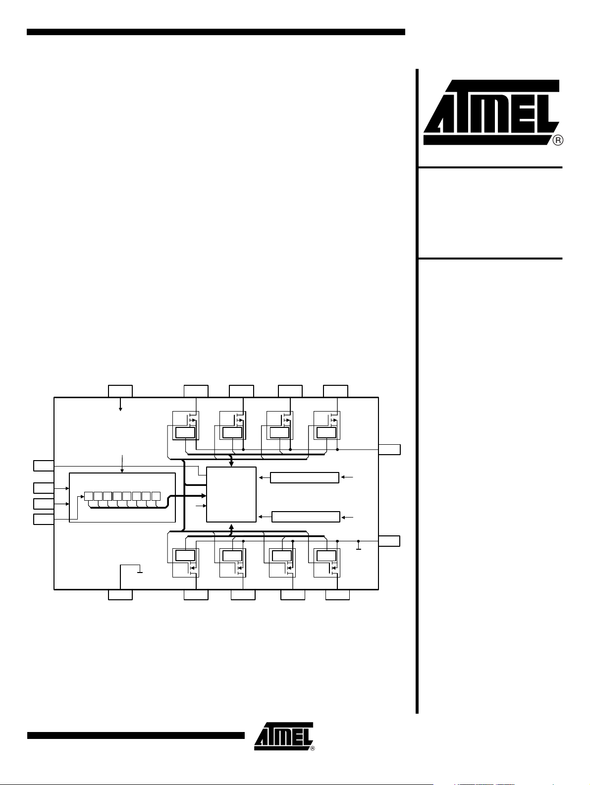
The U6820BM is a driver interface in BCDMOS technology with 8 independent driver
stages having a maximum current capability of 50 mA each. Its partitioning into 4
high-side and 4 low-side driver stages allows an easy connection of either 4 halfbridges or 2 H-bridges on the pc board. The U6820BM communicates with a microcontroller via an 8-bit serial interface. Integrated protection against short circuit and
overtemperature give added value. EMI protection and 2-kV ESD protection together
with automotive qualification referring to conducted interference (ISO/TR 7637/1)
make this IC ideal for both automotive and industrial applications.
Dual Quad
BCDMOS
Driver IC
U6820BM
Figure 1. Block Diagram
V
CC
6
V
CC
14
STATUS
HH
HH
L
S2S
S
1
4
Input Register
4
GND
CC
CLK
11
CS
12
13
DI
3SS4
HS4 HS3 HS2 HS1
16
Current
limiter
L
L
L
S
S
S
3
2
1
V
CC
Current
limiter
Current
limiter
Control
logic
Current
limiter
9
1015
8 1
Current
limiter
Thermal protection
Power-on reset
Current
limiter
Current
limiter
Current
limiter
3
V
S
V
CC
V
CC
5
GND
S
27
LS1LS2LS3LS4
Rev. 4527A–BCD–03/02
1
Page 2
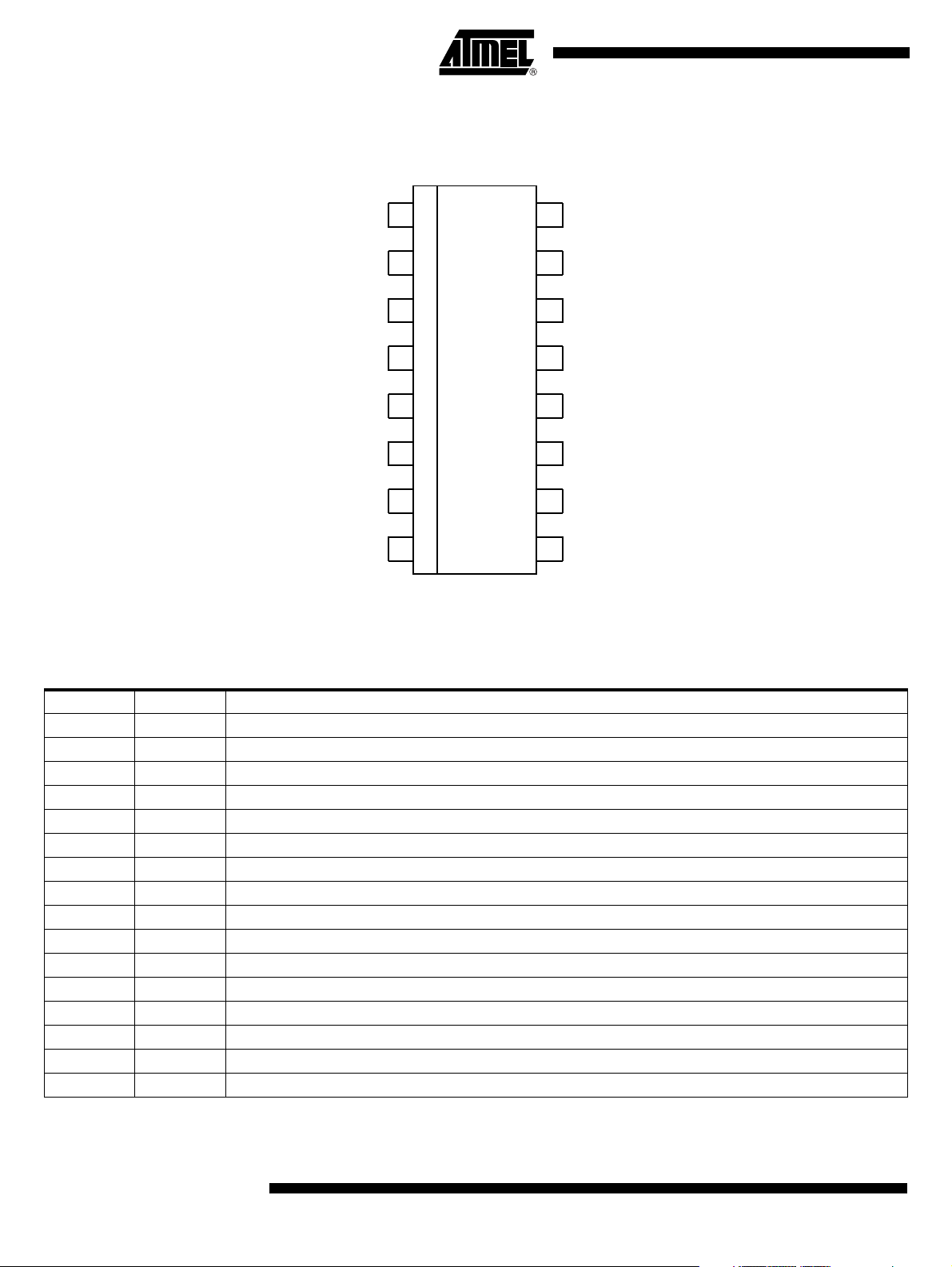
Pin Configuration
Figure 2. Pinning SO16
HS1
LS1
VS
GNDCC
GNDS
VCC
LS2
HS2
1
2
3
4
5
6
7
8
16
15
14
13
12
11
10
9
HS4
LS4
STATUS
DI
CLK
CS
LS3
HS3
Pin Description
Pin Symbol Function
1 HS1 Output high side 1
2 LS1 Output low side 1
3 VS Supply voltage 6 V to 18 V
4 GNDCC Digital ground
5 GNDS Power ground
6 VCC Supply voltage 5 V (external)
7 LS2 Output low side 2
8 HS2 Output high side 2
9 HS3 Output high side 3
10 LS3 Output low side 3
11 CS Set supply status (chip select)
12 CLK Clock line for 8-bit control shift register
13 DI Data line for 8-bit control shift register
14 STATUS Status output (H = fault, diagnostic “H” if all driver stages are switched off)
15 LS4 Output low side 4
16 HS4 Output high side 4
2
U6820BM
4527A–BCD–03/02
Page 3

U6820BM
Description of the
Control Interface to
the Microcontroller
The serial-parallel interface basically includes an 8-bit shift register (SR), an 8-bit command register (CR) and a 4-bit counter.
The data input takes place with commands at Pins DI (data input), CS (chip select) and
CLK (clock). With a falling edge at CLK, the information at DI is transferred into the SR.
The first information written into the SR is the least significant bit (LSB). The Pin STATUS is used for diagnostic purposes and reports any fault condition to the
microcontroller.
The input CS in accordance with the CR controls the serial interface. A high level at CS
disables the SR. With a falling edge at CS, the SR is enabled. The CR control allows
only the first 8 bits to be transferred into the SR, and further clocks at CLK are ineffective. If a rising edge occurs at CS after 8 clocks precisely, the information from the SR is
transferred into the CR. If the number of clock cycles during the low phase of CS was
less or more than eight transitions, no transfer will take place. A new command switches
the output stages on or off immediately.
Each output stage is controlled by one specific bit of the CR. Low level means “supply
off” or inactive, and high level means “supply on” or active. If all 8 bits are at a low level,
the output stages will be set into standby mode.
If one of the output stages detects a short circuit and additionally overtemperature condition, the corresponding control bit in the CR is set to low. This reset has priority over
an external command to CR, thus, this does not affect the 1
tects the IC against overtemperature by activating the temperature shut down
immediately.
st
control bit. The priority pro-
The STATUS Output The STATUS output is at low level during normal operation. If one or more output stages
detect short circuit or if overtemperature is indicated, the STATUS output changes to
high level (OR-connection).
For diagnostic purposes (self test of the status output), the status output can also be
brought into high level during standby mode.
Timing of the Status
Output Reset Signalizes
the Failure Mode
Power-on Reset After switching on the supply voltage, all data latches are reset and the outputs are
The use of different reset conditions at the STATUS output simplifies the failure analysis
during normal operation, and is also beneficial during testing.
The storage content can be used for STATUS output. It is indicated and latched immediately with the rising edge of CS at STATUS output if less than 8 clocks were received
during the low phase of CS. The reset is initiated by the falling edge of the 8
(bit 7) of the next data input.
Also, the appearance of more than 8 clocks is latched and indicated at STATUS by the
rising edge of the 9
(bit 1) of the next data input.
The detection of overtemperature is latched internally. It is reset by the falling edge of
th
clock (bit 3) of a data transfer if overtemperature is no longer present.
the 4
switched off. The typical power-on reset threshold is V
vated after the first data transfer.
th
clock. The reset is initiated by the falling edge of the 2nd clock
= 3.7 V. The outputs are acti-
CC
th
clock
4527A–BCD–03/02
3
Page 4
Short-circuit Protection The current of the output stages is limited by an active feedback control. Short circuit at
one output stage sets the diagnostic Pin 14 (STATUS) to high. In case of both conditions, short circuit at one of the outputs and temperature detection, the affected output is
switched off selectively. It will be activated again after the first new data transfer.
Inductance Protection Clamping diodes and FETs are integrated to protect the IC against too high or too low
voltages at the outputs. They prevent the IC from latch up and parasitic currents which
may exceed power dissipation.
Temperature Protection The IC is protected by an overtemperature detection. As soon as the junction tempera-
= 155°C typically is exceeded, the diagnostic Pin 14 (STATUS) is set “high”.
ture T
j
General overtemperature detection along with short-circuit condition at a specific output
result in temperature shut down at that specific output. After temperature shut down, the
data input register has to be set again with a hysteresis of typically
=140°C).
(T
j
∆T = 15 K
ESD Protection All output stages are protected against electrostatic discharge up to 5 kV (HBM) with
external components (see Figure 5), all other pins are protected up to 2 kV (HBM).
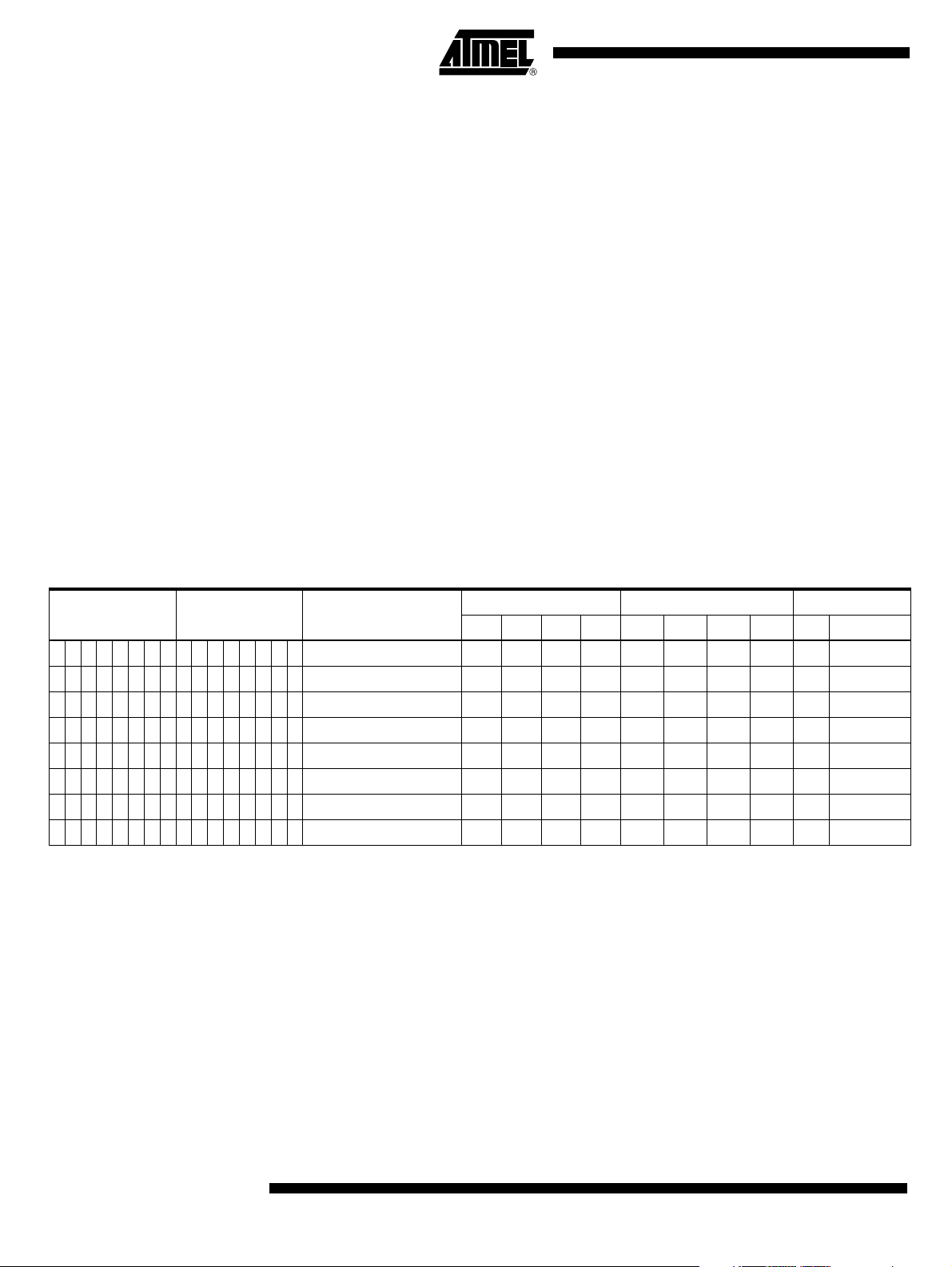
Table 1. Timing of the STATUS Output
Shift Register
0000000000000000 All out = OK off off off off off off off off H New CS
1111111111111111 All on = OK on on on on on on on on L
0000000100000001 E.g. one on = OK off off off off off off off on L
0111111101111111 Short at LS3 off on on on on on on on H No short
1111111111101111 Temp & short at HS4 on on on off on on on on H New CS4
1100001100000000 V
11100011xxxxxxxx CS with less 8 CLK x x x x x x x x H New CS 8
00011100xxxxxxxx CS with more 8 CLK x x x x x x x x H New CS 2
Command
Register
Condition
< 3.7 V = P-ON off off off off off off off off H P-ON, CS
VCC
Low-side Switch High-side Switch Status
LS1 LS2 LS3 LS4 HS1 HS2 HS3 HS4 Set Reset
4
U6820BM
4527A–BCD–03/02
Page 5

Figure 3. Data Transfer Timing Diagram
U6820BM
t
CSCLK
t
CLKP
t
CLKH
CLK
LSB MSB
t
CLKCS
t
CLKL
DI
t
DICLKtDIH/L
CS
Table 2. AC Characteristics for Testing
90 %
t
t
r
f
90 %
10%
50%
50%
t
CLKCSH
50%
t
CS
Specification Conditions Minimum Maximum Unit
t
(rise) 10% to 90% VCC on CLK, DI and CS 10 ns
r
t
(fall) 10% to 90% VCC on CLK, DI and CS 10 ns
f
t
CLKP
t
CLKH
t
CLKL
t
CLKCS
t
CSCLK
t
DICLK
t
DIH/L
t
CLKCSH
t
CS
1/2 V
1/2 V
1/2 V
1/2 V
1/2 V
1/2 V
1/2 V
1/2 V
1/2 V
CC
CC
CC
CC
CC
CC
CC
CC
CC
250 ns
100 ns
100 ns
150 ns
100 ns
80 ns
100 ns
100 ns
250 ns
4527A–BCD–03/02
5
Page 6

Figure 4. Block Diagram of the Control Interface
Serial-Parallel Interface
CS
11
8CLK
CLK
12
13
DI
Load CR
EN
1
CL
R
Q0
EN
H4
CL
DIN
Q7
DIN
CL
NR NQ
CLK
2
Q1
H3
Q6
DIN
NR NQ
4
Counter
Q2
h if 2
Q3
h if 4
H2Q4H1
Shift register SR
Q5
DIN
DIN
Command register BR
NR NQ
NR NQ
8
h if 8
L4
Q3
DIN
NR NQ
L3
Q2
DIN
NR NQ
DFF
D
R
CL NQ
NR NQ
Q CL
DFF
D
R NQ
POR norm=0
L2
L1
LSB
Q1
DIN
Q0
DIN
NR NQ
DFF
D
Q
R
CL NQ
Q
DFF
D Q
R
CL NQ
P-ON-Reset
Th-protection
All norm = 0
DFF
D Q
CL
R
NQ
14
STATUS
norm = 0
4
S
H
_
C
S
I
3
S
H
N
_
O
C
_
S
I
4
S
H
2
S
H
N
_
O
C
_
S
I
3
S
H
1
S
H
N
_
O
C
_
S
I
2
S
H
4
S
L
N
_
O
C
_
S
I
1
S
H
3
S
L
N
_
C
O
_
S
I
4
S
L
2
S
L
N
_
C
O
_
S
I
3
S
L
1
S
L
N
O
_
2
S
L
N
_
C
O
_
S
I
1
S
L
0
Y
=
B
m
_
r
D
o
T
n
S
6
U6820BM
4527A–BCD–03/02
Page 7

U6820BM
Absolute Maximum Ratings
Parameters Pin Symbol Minimum Maximum Unit
Supply voltage 3 V
Logic supply voltage 6 V
VS
VCC
Logic input voltage 11, 12 13 CS, CLK, DI -0.3 V
Logic output voltage 14 STATUS -0.3 V
Input current 3 I
6I
Output current
(internally limitted)
1-2, 8-11, 15-16 I
Junction temperature range T
Storage temperature range T
1H-4H
VS
VCC
and I
j
stg
1L-4L
Thermal Resistance
Parameters Symbol Value Unit
Junction ambient R
Junction case R
thJA
thJC
-0.3 +40 V
-0.3 +7 V
+ 0.5 V
VCC
+ 0.3 V
VCC
0.2 mA
5mA
30 65 mA
-40 +150 °C
-55 +150 °C
110 K/W
26 K/W
Operating Range
Parameters Pin Symbol Value Unit
Supply voltage 3 V
Logic supply voltage 6 V
VS
VCC
Logic input voltage low 11, 12, 13 CS, CLK, DI -0.2 to (0.2 x V
Logic input voltage high 11, 12, 13 CS, CLK, DI (0.7 x V
Logic output voltage (1 mA load) 14 STATUS 0.5 to (V
Clock frequency f
Junction temperature range T
CLK
j
6 to 18 V
4.5 to 5.5 V
)V
VCC
VCC
) to (V
+ 0.3) V
VCC
- 1) V
VCC
5MHz
-40 to +150 °C
4527A–BCD–03/02
7
Page 8

Electrical Characteristics
7V < VVS < 40 V; 4.5 V < V
> 5.5 V; -40°C < Tj < 150°C; unless otherwise specified
VCC
No. Parameters Test Conditions Pin Symbol Min. Typ. Max. Unit Type*
1 Current Consumption
1.1 Supply current VS No external load 3 I
1.2 Supply current VCC No external load 6 I
1.3 Power-on reset threshold 6 V
1.4 Power-on reset delay time After switching on V
CC
6T
VS
VCC
CC POR
d POR
3.4 3.7 4.0 V A
60 95 130 µs D
0.2 mA A
5mAA
2 Thermal Shutdown
2.1 Thermal shutdown set t
2.2 Thermal shutdown reset t
j PW set
j PW reset
140 155 165 °CA
130 135 155 °CA
2.3 Thermal hysteresis Dt 20 K A
3 Output Specifications (1L - 4L, 1H - 4H)
3.1 On-resistance low I
3.2 On-resistance high I
3.3 Output leakage current
lowside
3.4 Output leakage current
highside
= 26 mA,
out
= 125°C
T
j
= 26 mA,
out
= 125°C
T
j
V
LSIDE 1-4
V
HSIDE 1-4
= 17.5 V 2, 7,
= 0.5 V 1, 8,
2, 7,
10, 15
1, 8,
9, 16
10, 15
9, 16
R
DSONLOW
R
DSONHIGH
I
LOWSIDE
I
HIGHSIDE
347Ω A
46.2510 Ω A
5µAA
-5 µA A
3.5 Output leakage steepness 1-2,
7-10,
dV
OUT/ dt
50 200 400 mV/µs D
15-16
3.6 Over current limitation
highside
3.7 Over current limitation
lowside
1, 8,
9, 16
2, 7,
10, 15
I
HIGHSIDE
I
LOWSIDE
27 45 95 mA A
27 45 80 mA A
4 Serial Interface – Inputs: CS, CLK and DATA
4.1 Input voltage low level
threshold
4.2 Input voltage high level
threshold
11-1 3
11-1 3
V
V
ILOW
IHIGH
4.3 Hysteresis of input voltage 11-13 ∆V
4.4 Pull-down current (internal pull-up
11-1 3
resistor:
0.7×
V
VCC
i
I
i
300 mV A
0.2×
V
VCC
VA
VA
300 µA A
30 kΩ to 140 kΩ)
5 Serial Interface – Output: STATUS
5.1 Output voltage low level I = 1 mA V
5.2 Output voltage high level I = 1 mA V
OLOW
OHIGH
V
-1 V
VCC
0.5 V A
VCC
VA
*) Type means: A =100% tested, B = 100% correlation tested, C = Characterized on samples, D = Design parameter
8
U6820BM
4527A–BCD–03/02
Page 9

Figure 5. Application Circuit
U6820BM
V
CC
5 V
µC
Typical application with
4 Hall-ICs for rotational speed detection
+
33µF
100nF
V
CC
6
U6820BM
V
CC
14
STATUS
HH
S
1
GND
L
L
L
S
S
S
3
4
2
4
CC
CLK
11
CS
HH
3SS4S2
12
13
DI
Sensor
control
Input register
RR
4.7nF
4.7nF
HS4
16
&XUUHQW
OLPLWHU
L
S
1
&XUUHQW
OLPLWHU
Control
HS3
9
LR
R * R * R *R *
4.7nF
RF
4.7nF
HS2 HS1
LF
V
BATT
12 V
8 1
&XUUHQW
OLPLWHU
Thermal protection
&XUUHQW
OLPLWHU
3
V
S
V
CC
100nF
+
47µF
logic
V
4.7nF
27k
&XUUHQW
OLPLWHU
CC
&XUUHQW
OLPLWHU
1015
4.7nF
100
27k
100
Power-on reset
&XUUHQW
OLPLWHU
4.7nF
27k
V
CC
5
GND
S
&XUUHQW
OLPLWHU
27
LS2LS3LS4
100
LS1
4.7nF
100
27k
R * = ca. 4 Ohm (I Lim for inv. supply)
Note: It is strongly recommended to connect the blocking capacitors at VS and VCC as close as possible to the power supply and GND
pins. Recommended value for V
depends on external loads, noise and surge immunity efforts. Recommended value for V
is less than 100 µF electrolytic in parallel with 100 nF ceramic. Value for electrolytic capacitor
S
is 33 µF electrolytic in parallel with
CC
100 nF ceramic. The 4-Ω resistors connected to the Pins HS1 - HS4 support the protection in case of a short circuit of these
pins to V
4527A–BCD–03/02
Batt
.
9
Page 10

Ordering Information
Extended Type Number Package Remarks
U6820BM-FP SO16
Package Information
Package SO16
Dimensions in mm
5.2
10.0
9.85
1.4
0.4
1.27
8.89
16 9
18
0.25
0.10
technical drawings
according to DIN
specifications
4.8
3.7
3.8
6.15
5.85
0.2
13036
10
U6820BM
4527A–BCD–03/02
Page 11

Atmel Headquarters Atmel Operations
Corporate Headquarters
2325 Orchard Parkway
San Jose, CA 95131
TEL 1(408) 441-0311
FAX 1(408) 487-2600
Europe
Atmel SarL
Route des Arsenaux 41
Casa Postale 80
CH-1705 Fribourg
Switzerland
TEL (41) 26-426-5555
FAX (41) 26-426-5500
Asia
Atmel Asia, Ltd.
Room 1219
Chinachem Golden Plaza
77 Mody Road Tsimhatsui
East Kowloon
Hong Kong
TEL (852) 2721-9778
FAX (852) 2722-1369
Japan
Atmel Japan K.K.
9F, Tonetsu Shinkawa Bldg.
1-24-8 Shinkawa
Chuo-ku, Tokyo 104-0033
Japan
TEL (81) 3-3523-3551
FAX (81) 3-3523-7581
Memory
Atmel Corporate
2325 Orchard Parkway
San Jose, CA 95131
TEL 1(408) 436-4270
FAX 1(408) 436-4314
Microcontrollers
Atmel Corporate
2325 Orchard Parkway
San Jose, CA 95131
TEL 1(408) 436-4270
FAX 1(408) 436-4314
Atmel Nantes
La Chantrerie
BP 70602
44306 Nantes Cedex 3, France
TEL (33) 2-40-18-18-18
FAX (33) 2-40-18-19-60
ASIC/ASSP/Smart Cards
Atmel Rousset
Zone Industrielle
13106 Rousset Cedex, France
TEL (33) 4-42-53-60-00
FAX (33) 4-42-53-60-01
Atmel Colorado Springs
1150 East Cheyenne Mtn. Blvd.
Colorado Springs, CO 80906
TEL 1(719) 576-3300
FAX 1(719) 540-1759
RF/Automotive
Atmel Heilbronn
Theresienstrasse 2
Postfach 3535
74025 Heilbronn, Germany
TEL (49) 71-31-67-0
FAX (49) 71-31-67-2340
Atmel Colorado Springs
1150 East Cheyenne Mtn. Blvd.
Colorado Springs, CO 80906
TEL 1(719) 576-3300
FAX 1(719) 540-1759
Biometrics/Imaging/Hi-Rel MPU/
High Speed Converters/RF Datacom
Atmel Grenoble
Avenue de Rochepleine
BP 123
38521 Saint-Egreve Cedex, France
TEL (33) 4-76-58-30-00
FAX (33) 4-76-58-34-80
Atmel Smart Card ICs
Scottish Enterprise Technology Park
Maxwell Building
East Kilbride G75 0QR, Scotland
TEL (44) 1355-803-000
FAX (44) 1355-242-743
e-mail
literature@atmel.com
Web Site
http://www.atmel.com
© Atmel Corporation 2002.
Atmel Corporation makes no warranty for the use of its products, other than those expressly contained in the Company’s standard warranty
which is detailed in Atmel’s Terms and Conditions located on the Company’s web site. The Company assumes no responsibility for any errors
which may appear in this document, reserves the right to change devices or specifications detailed herein at any time without notice, and does
not make any commitment to update the information contained herein. No licenses to patents or other intellectual property of Atmel are granted
by the Company in connection with the sale of Atmel products, expressly or by implication. Atmel’s products are not authorized for use as critical
components in life support devices or systems.
Atmel® is the registered trademark of Atmel.
Other terms and product names may be the trademarks of others.
Printed on recycled paper.
4527A–BCD–03/02
xM
 Loading...