

Page 1

Features
• Supply Voltage 4.5 V to 5.5 V
• Operating Temperature Range -40°C to +85°C
• Minimal External Circuitry Requirements, No RF Components on the PC Board Except
Matching to the Receiver Antenna
• High Sensitivity, Especially at Low Data Rates
• Sensitivity Reduction Possible Even While Receiving
• Fully Integrated VCO
• Low Power Consumption Due to Configurable Self Polling with a Programmable Time
Frame Check
• Single-ended RF Input for Easy Matching to l/4 Antenna or Printed Antenna on PCB
• Low-cost Solution Due to High Integration Level
• ESD Protection According to MIL-STD 883 (4 KV HBM) Except Pin POUT (2 KV HBM)
• High Image Frequency Suppression Due to 1 MHz IF in Conjunction with a SAW Front-
end Filter. Up to 40 dB is Thereby Achievable with Newer SAWs
• Programmable Output Port for Sensitivity Selection or for Controlling External
Periphery
• Communication to the Microcontroller Possible via a Single, Bi-directional Data Line
• Power Management (Polling) is also Possible by Means of a Separate Pin via the
Microcontroller
Description
The U3745BM is a multi-chip PLL receiver device supplied in an SO20 package. It has
been specially developed for the demands of RF low-cost data transmission systems
with low data rates from 1 kBaud to 10 kBaud in Manchester or Bi-phase code. The
receiver is well suited to operate with Atmel’s PLL RF transmitter U2745B. It can be
used in the frequency receiving range of f
mission. All the statements made below refer to 433.92-MHz and 315-MHz
applications.
The main applications of the U3745BM are in the areas of outside temperature metering, socket control, garage door opener, consumption metering, light/fan or aircondition control, jalousies, wireless keyboard and various other consumer market
applications.
= 310 MHz to 440 MHz for ASK data trans-
0
UHF ASK
Receiver IC
U3745BM
Rev. 4663A–RKE–06/03
1
Page 2
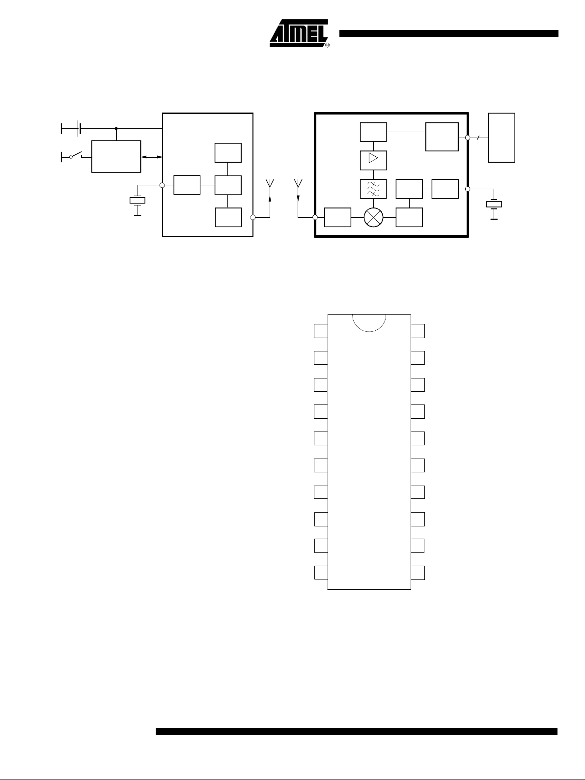
System Block Diagram
1 Li cell
Encoder
M44Cx9x
Keys
Pin Configuration
UHF ASK/FSK
Remote control transmitter
U2745B
PLL
XTO
VCO
Power
amp.
Figure 1. Pinning SO20
Antenna Antenna
NC
ASK
CDEM
UHF ASK
Remote control receiver
U3745BM
Demod.
IF Amp
LNA VCO
1
2
3
Data
interface
PLL XTO
20
DATA
19
ENABLE
18
TEST
1...3
µC
AVCC
AGND
DGND
MIXVCC
LNAGND
LNA_IN
NC
4
5
17
16
POUT
MODE
U3745BM
6
7
8
9
10
15
14
13
12
11
DVCC
XTO
LFGND
LF
LFVCC
2
U3745BM
4663A–RKE–06/03
Page 3

Pin Description
Pin Symbol Function
1 NC Not connected
2 ASK ASK high
3 CDEM Lower cut-off frequency data filter
4 AVCC Analog power supply
5 AGND Analog ground
6 DGND Digital ground
7 MIXVCC Power supply mixer
8 LNAGND High-frequency ground LNA and mixer
9LNA_INRF input
10 NC Not connected
11 LFVCC Power supply VCO
12 LF Loop filter
13 LFGND Ground VCO
14 XTO Crystal oscillator
15 DVCC Digital power supply
16 MODE Selecting 433.92 MHz/315 MHz. Low: 4.90625 MHz (USA), High: 6.76438 (Europe)
17 POUT Programmable output port
18 TEST Test pin, during operation at GND
19 ENABLE Enables the polling mode. Low: polling mode off (sleep mode). High: polling mode on (active mode)
20 DATA Data output/configuration input
U3745BM
4663A–RKE–06/03
3
Page 4
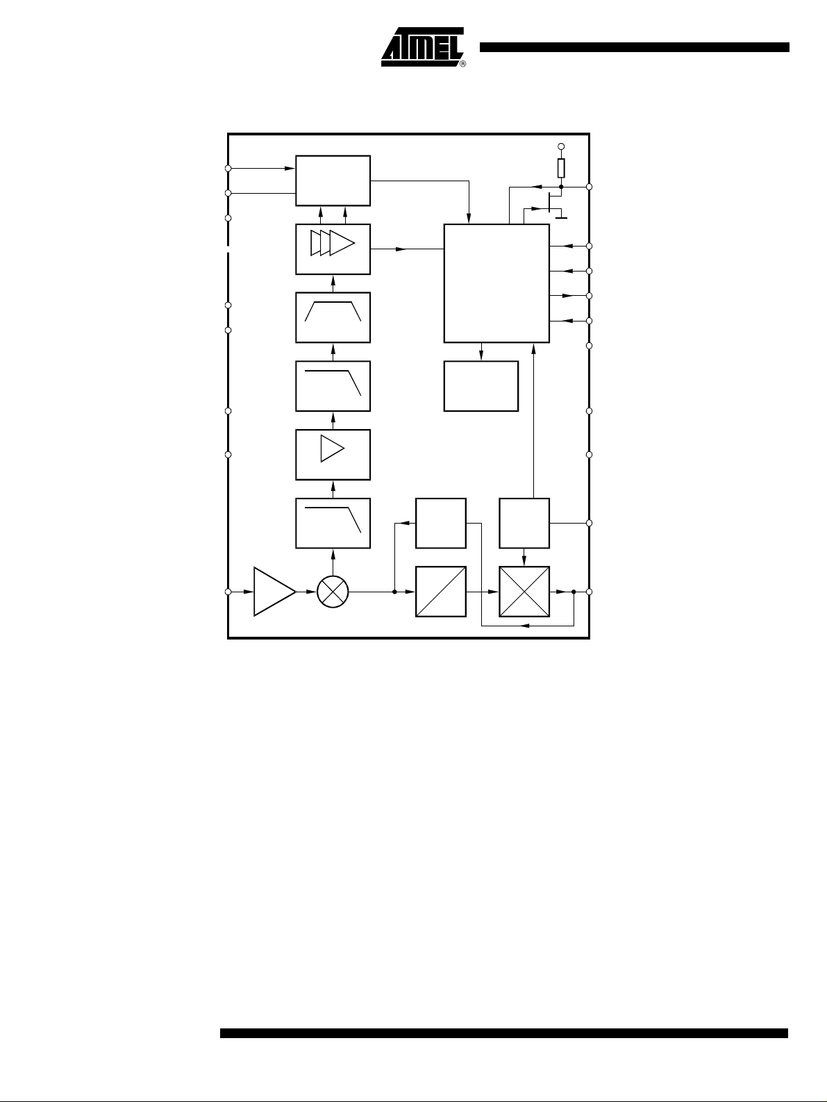
Block Diagram
ASK
CDEM
AVCC
Demodulator
and data filter
Limiter outRSSI
DEMOD_OUT
50 kW
V
S
DATA
AGND
DGND
MIXVCC
LNAGND
LNA_IN
LNA
IF Amp
4th Order
LPF
3 MHz
IF Amp
LPF
3 MHz
Sensitivity
reduction
Polling circuit
and
control logic
FE CLK
Standby logic
VCO XTO
f
¸ 64
ENABLE
TEST
POUT
MODE
DVCC
LFGND
LFVCC
XTO
LF
4
U3745BM
4663A–RKE–06/03
Page 5
RF Front End
U3745BM
The RF front end of the receiver is a heterodyne configuration that converts the input
signal into a 1-MHz IF signal. According to the block diagram, the front end consists of
an LNA (low noise amplifier), LO (local oscillator), a mixer and RF amplifier.
The LO generates the carrier frequency for the mixer via a PLL synthesizer. The XTO
(crystal oscillator) generates the reference frequency f
oscillator) generates the drive voltage frequency f
the voltage at pin LF. f
by the phase frequency detector. The current output of the phase frequency
to f
XTO
is divided by a factor of 64. The divided frequency is compared
LO
LO
detector is connected to a passive loop filter and thereby generates the control voltage
for the VCO. By means of that configuration, VLF is controlled in a way that fLO/64 is
V
LF
equal to f
f
XTO
. If fLO is determined, f
XTO
f
LO
--------=
64
can be calculated using the following formula:
XTO
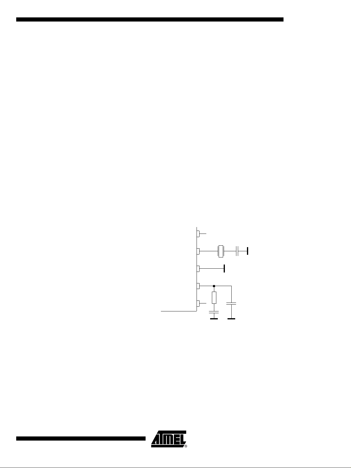
The XTO is a one-pin oscillator that operates at the series resonance of the quartz crystal. According to Figure 2, the crystal should be connected to GND via a capacitor CL.
The value of that capacitor is recommended by the crystal supplier. The value of CL
should be optimized for the individual board layout to achieve the exact value of f
hereby of f
. When designing the system in terms of receiving bandwidth, the accuracy
LO
of the crystal and XTO must be considered.
. The VCO (voltage-controlled
XTO
for the mixer. fLO is dependent on
and
XTO
Figure 2. PLL Peripherals
V
S
DVCC
C
L
XTO
LFGND
R1 = 820 W
C9 = 4.7 nF
LF
LFVCC
R1
V
S
C9
C10 = 1 nF
C10
The passive loop filter connected to Pin LF is designed for a loop bandwidth of
BLoop = 100 kHz. This value for BLoop exhibits the best possible noise performance of
the LO. Figure 2 shows the appropriate loop filter components to achieve the desired
loop bandwidth. If the filter components are changed for any reason, please note that
the maximum capacitive load at Pin LF is limited. If the capacitive load is exceeded, a bit
check may no longer be possible since f
cannot settle in time before the bit check
LO
starts to evaluate the incoming data stream. Therefore, self polling also does not work in
that case.
4663A–RKE–06/03
is determined by the RF input frequency fRF and the IF frequency fIF using the follow-
f
LO
ing formula:
f
LOfRFfIF
–=
5
Page 6

To determine fLO, the construction of the IF filter must be considered at this point. The
nominal IF frequency is f
quencies, the filter is tuned by the crystal frequency f
fixed relation between f
= 1 MHz. To achieve a good accuracy of the filter’s corner fre-
IF
and fLO that depends on the logic level at pin mode. This is
IF
. This means that there is a
XTO
described by the following formulas:
f
MODE 0 (USA) f
MODE 0 (Europe) f
IF
IF
LO
----------==
314
f
LO
------------- -----==
432.92
The relation is designed to achieve the nominal IF frequency of f
applications. For applications where f
case of f
not equal to 1 MHz. f
= 433.92 MHz, the MODE must be set to ‘1’. For other RF frequencies, fIF is
RF
is then dependent on the logical level at Pin MODE and on fRF.
IF
= 315 MHz, the MODE must be set to ‘0’. In the
RF
= 1 MHz for most
IF
Table 1 summarizes the different conditions.
The RF input either from an antenna or from a generator must be transformed to the RF
input pin LNA_IN. The input impedance of that pin is provided in the electrical parameters. The parasitic board inductances and capacitances also influence the input
matching. The RF receiver U3745BM exhibits its highest sensitivity at the best signal-tonoise ratio in the LNA. Hence, noise matching is the best choice for designing the transformation network.
A good practice when designing the network is to start with power matching. From that
starting point, the values of the components can be varied to some extent to achieve the
best sensitivity.
If a SAW is implemented into the input network, a mirror frequency suppression of
DP
= 40 dB can be achieved. There are SAWs available that exhibit a notch at
Ref
Df = 2 MHz. These SAWs work best for an intermediate frequency of IF = 1 MHz. The
selectivity of the receiver is also improved by using a SAW. In typical automotive applications, a SAW is used.
Figure 3 shows a typical input matching network for f
= 433.92 MHz using a SAW. Figure 4 illustrates an input matching to 50 W without a
f
RF
= 315 MHz and
RF
SAW. The input matching networks shown in Figure 4 are the reference networks for the
parameters given in the section “Electrical Characteristics”.
Table 1. Calculation of LO and IF Frequency
Conditions Local Oscillator Frequency Intermediate Frequency
fRF = 315 MHz, MODE = 0 fLO = 314 MHz fIF = 1 MHz
f
= 433.92 MHz, MODE = 1 fLO = 432.92 MHz fIF = 1 MHz
RF
300 MHz < f
365 MHz < f
6
< 365 MHz, MODE = 0
RF
< 450 MHz, MODE = 1
RF
U3745BM
LO
f
LO
1
------------ ------------- ---=
1
1
----------+
314
f
RF
1
------------ ------+
432.92
f
f
RF
------------ -------=
f
f
LO
f
----------=
IF
314
f
LO
------------ ------=
IF
432.92
4663A–RKE–06/03
Page 7
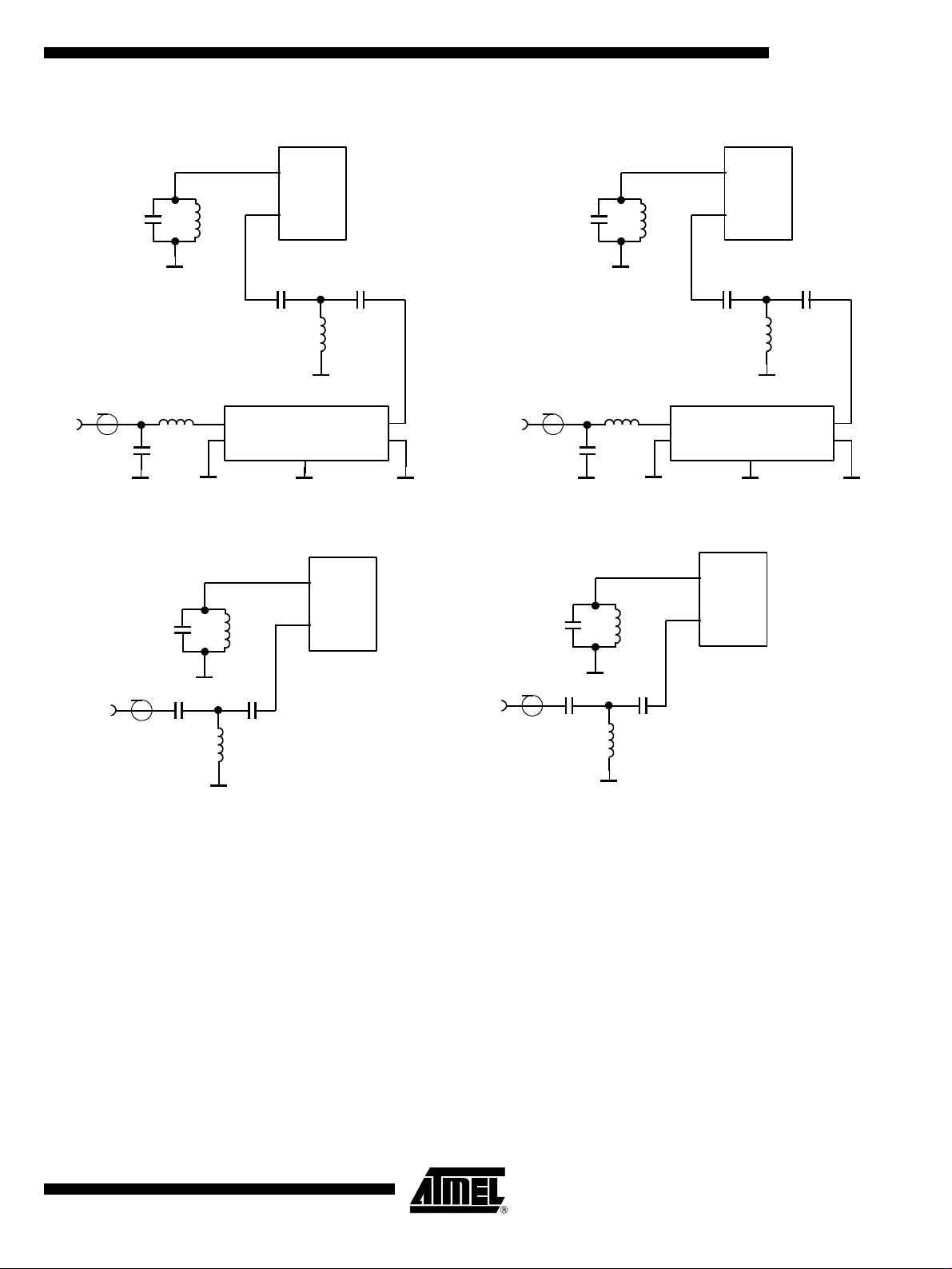
Figure 3. Input Matching Network with SAW Filter
U3745BM
8
LNAGND
U3745BM
IN
IN_GND
9
LNA_IN
C16
100p
27n
B3555
CASE_GND
3,4 7,8
L3
C17
8.2p
TOKO LL2012
F27NJ
OUT
OUT_GND
5
6
C3
22p
fRF = 433.92 MHz
C2
8.2p
TOKO LL2012
F33NJ
RF
IN
L2
33n
L
25n
1
2
Figure 4. Input Matching Network without SAW Filter
fRF = 433.92 MHz
15p
25n
8
LNAGND
U3745BM
9
LNA_IN
fRF = 315 MHz
RF
IN
10p
fRF = 315 MHz
33p
C3
47p
C2
L2
TOKO LL2012
F82NJ
82n
25n
L
25n
1
2
IN
IN_GND
8
9
8
LNAGND
U3745BM
9
LNA_IN
C16
100p
L3
47n
B3551
CASE_GND
3,4 7,8
LNAGND
U3745BM
LNA_IN
C17
22p
TOKO LL2012
F47NJ
OUT
OUT_GND
5
6
RF
RF
IN
3.3p
22n
100p
TOKO LL2012
F22NJ
IN
3.3p
39n
100p
TOKO LL2012
F39NJ
Please note that for all coupling conditions (see Figure 3 and Figure 4), the bond wire
inductivity of the LNA ground is compensated. C3 forms a series resonance circuit
together with the bond wire. L = 25 nH is a feed inductor to establish a DC path. Its
value is not critical but must be large enough not to detune the series resonance circuit.
For cost reduction, this inductor can be easily printed on the PCB. This configuration
improves the sensitivity of the receiver by about 1 dB to 2 dB.
4663A–RKE–06/03
7
Page 8

Analog Signal Processing
IF Amplifier The signals coming from the RF front end are filtered by the fully integrated 4th-order IF
filter. The IF center frequency is f
= 433.92 MHz is used. For other RF input frequencies, refer to Table 1 to determine
f
RF
the center frequency.
= 1 MHz for applications where fRF= 315 MHz or
IF
The receiver U3745BM employs an IF bandwidth of B
= 600 kHz. This IC can be used
IF
together with the U2745B. SAW transmitters exhibit much higher transmit frequency tolerances compared to PLL transmitters. Generally, it is necessary to use B
= 600 kHz
IF
together with such transmitters.
RSSI Amplifier The subsequent RSSI amplifier enhances the output signal of the IF amplifier before it is
= 60 dB. If the
RSSI
Demodulator and Data
Filter
fed into the demodulator. The dynamic range of this amplifier is DR
RSSI amplifier is operated within its linear range, the best S/N ratio is maintained in ASK
mode. If the dynamic range is exceeded by the transmitter signal, the S/N ratio is
defined by the ratio of the maximum RSSI output voltage and the RSSI output voltage
due to a disturber. The dynamic range of the RSSI amplifier is exceeded if the RF input
signal is about 60 dB higher compared to the RF input signal at full sensitivity.
Since different RF input networks may exhibit slightly different values for the LNA gain,
the sensitivity values given in the electrical characteristics refer to a specific input
matching. This matching is illustrated in Figure 4 and exhibits the best possible
sensitivity.
The signal coming from the RSSI amplifier is converted into the raw data signal by the
ASK demodulator.
In ASK mode, an automatic threshold control circuit (ATC) is employed to set the detection reference voltage to a value where a good signal-to-noise ratio is achieved. This
circuit also implies the effective suppression of any kind of in-band noise signals or competing transmitters. If the S/N ratio exceeds 10 dB, the data signal can be detected
properly.
The output signal of the demodulator is filtered by the data filter before it is fed into the
digital signal processing circuit. The data filter improves the S/N ratio as its bandpass
can be adopted to the characteristics of the data signal. The data filter consists of a 1storder high-pass and a 1st-order low-pass filter.
The high-pass filter cut-off frequency is defined by an external capacitor connected to
pin CDEM. The cut-off frequency of the high-pass filter is defined by the following
formula:
f
cu_DF
------------ ------------- ------------- ---------- -----------=
2
1
p´ 30 kW´ CDEM´
In self-polling mode, the data filter must settle very rapidly to achieve a low current consumption. Therefore, CDEM cannot be increased to very high values if self polling is
used. On the other hand, CDEM must be large enough to meet the data filter requirements according to the data signal. Recommended values for CDEM are given in the
section “Electrical Characteristics”.
The cut-off frequency of the low-pass filter is defined by the selected baud rate range
(BR_Range). BR_Range is defined in the OPMODE register (refer to section “Configuration of the Receiver”). BR_Range must be set in accordance to the used baud rate.
8
U3745BM
4663A–RKE–06/03
Page 9
U3745BM
The U3745BM is designed to operate with data coding where the DC level of the data
signal is 50%. This is valid for Manchester and Bi-phase coding. If other modulation
schemes are used, the DC level should always remain within the range of V
and V
= 66%. The sensitivity may be reduced by up to 1.5 dB in that condition.
DC_max
Each BR_Range is also defined by a minimum and a maximum edge-to-edge time
). These limits are defined in the section “Electrical Characteristics”. They should
(t
ee_sig
not be exceeded to maintain full sensitivity of the receiver.
DC_min
=33%
Receiving
Characteristics
The RF receiver U3745BM can be operated with and without a SAW front end filter. The
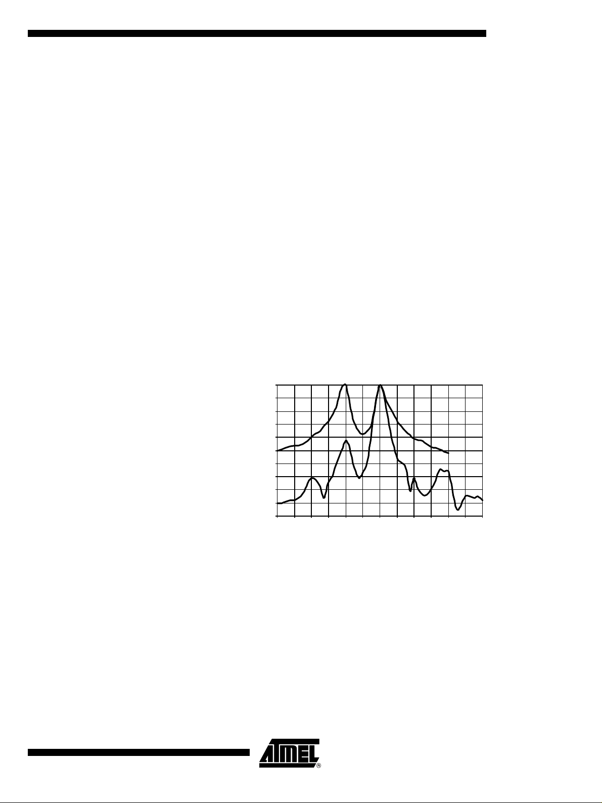
selectivity with and without a SAW front-end filter is illustrated in Figure 5. This example
relates to ASK mode of the U3745BM. Note that the mirror frequency is reduced by
40 dB. The plots are printed relatively to the maximum sensitivity. If a SAW filter is used,
an insertion loss of about 4 dB must be considered.
When designing the system in terms of receiving bandwidth, the LO deviation must be
considered as it also determines the IF center frequency. The total LO deviation is calculated to be the sum of the deviation of the crystal and the XTO deviation of the
U3745BM. Low-cost crystals are specified to be within ±100 ppm. The XTO deviation of
the U3745BM is an additional deviation due to the XTO circuit. This deviation is specified to be ±50 ppm. If a crystal of ±100 ppm is used, the total deviation is ±150 ppm in
that case. Note that the receiving bandwidth and the IF-filter bandwidth are equivalent in
ASK mode.
Figure 5. Receiving Frequency Response
0.0
-10.0
-20.0
-30.0
-40.0
-50.0
-60.0
dP (dB)
-70.0
-80.0
-90.0
-100.0
-6.0 -5.0 -4.0 -3.0 -2.0 -1.0 0.0 1.0 2.0 3.0 4.0 5.0 6.0
df (MHz)
without SAW
with SAW
4663A–RKE–06/03
9
Page 10

Polling Circuit and Control Logic
The receiver is designed to consume less than 1 mA while being sensitive to signals
from a corresponding transmitter. This is achieved via the polling circuit. This circuit
enables the signal path periodically for a short time. During this time the bit check logic
verifies the presence of a valid transmitter signal. Only if a valid signal is detected the
receiver remains active and transfers the data to the connected microcontroller. If there
is no valid signal present, the receiver is in sleep mode most of the time resulting in low
current consumption. This condition is called polling mode. A connected microcontroller
is disabled during that time.
All relevant parameters of the polling logic can be configured by the connected microcontroller. This flexibility enables the user to meet the specifications in terms of current
consumption, system response time, data rate etc.
Regarding the number of connection wires to the µC, the receiver is very flexible. It can
be either operated by a single bi-directional line to save ports to the connected microcontroller, or it can be operated by up to three uni-directional ports.
Basic Clock Cycle of the
Digital Circuitry
The complete timing of the digital circuitry and the analog filtering is derived from one
clock. According to Figure 6, this clock cycle T
is derived from the crystal oscillator
Clk
(XTO) in combination with a divider. The division factor is controlled by the logical state
at pin MODE. According to section “RF Front End”, the frequency of the crystal oscillator
) is defined by the RF input signal (f
(f
XTO
of the local oscillator (f
LO
).
) which also defines the operating frequency
RFin
Figure 6. Generation of the Basic Clock Cycle
T
Clk
Divider
:14/:10
XTO
f
XTO
MODE
16
DVCC
15
XTO
14
Pin MODE can now be set in accordance with the desired clock cycle T
L : USA (:10)
H: Europe (:14)
Clk
. T
controls
Clk
the following application-relevant parameters:
• Timing of the polling circuit including bit check
• Timing of analog and digital signal processing
• Timing of register programming
• Frequency of the reset marker
• F filter center frequency (f
Most applications are dominated by two transmission frequencies: f
mainly used in the USA, f
-dependent parameters, the electrical characteristics display three conditions for
T
Clk
Send
)
IF0
= 315 MHz is
Send
= 433.92 MHz in Europe. In order to ease the usage of all
each parameter.
10
U3745BM
4663A–RKE–06/03
Page 11

U3745BM
• USA Applications
= 4.90625 MHz, MODE = L, T
(f
XTO
• Europe Applications
= 6.76438 MHz, MODE = H, T
(f
XTO
• Other applications
is dependent on f
(T
Clk
and on the logical state of pin MODE. The electrical
XTO
characteristic is given as a function of T
The clock cycle of some function blocks depends on the selected baud rate range
(BR_Range) which is defined in the OPMODE register. This clock cycle T
by the following formulas for further reference:
= 2.0383 µs)
Clk
= 2.0697 µs)
Clk
).
Clk
is defined
XClk
T
T
T
XClk
XClk
XClk
XClk
= 8 ´ T
= 4 ´ T
= 2 ´ T
= 1 ´ T
Clk
Clk
Clk
Clk
BR_Range = BR_Range0: T
BR_Range1:
BR_Range2:
BR_Range3:
Polling Mode According to Figure 3, the receiver stays in polling mode in a continuous cycle of three
different modes. In sleep mode, the signal processing circuitry is disabled for the time
period T
while consuming low current of IS=I
Sleep
all signal processing circuits are enabled and settled. In the following bit check mode,
the incoming data stream is analyzed bit by bit contra a valid transmitter signal. If no
valid signal is present, the receiver is set back to sleep mode after the period T
This period varies check by check as it is a statistical process. An average value for
T
current consumption is I
is given in the section “Electrical Characteristics”. During T
Bitcheck
S
=I
. The average current consumption in polling mode is
Son
dependent on the duty cycle of the active mode and can be calculated as:
I
Spoll
During T
I
SoffTSleepISonTStartupTBitcheck
------------ ------------- ------------- ----------- ------------ ------------- ------------- ------------- ------=
T
++
SleepTStartupTBitcheck
Sleep
and T
, the receiver is not sensitive to a transmitter signal. To guaran-
Startup
+()´+´
tee the reception of a transmitted command, the transmitter must start the telegram with
an adequate preburst. The required length of the preburst is dependent on the polling
parameters T
Start,µC
). T
Bitcheck
(T
, T
Sleep
thus depends on the actual bit rate and the number of bits (N
Startup
, T
and the startup time of a connected microcontroller
Bitcheck
be tested.
. During the start-up period, T
Soff
and T
Startup
Startup
Bitcheck
Bitcheck
Bitcheck
the
) to
,
.
The following formula indicates how to calculate the preburst length.
T
Preburst
³ T
Sleep
+ T
Startup
Sleep Mode The length of period T
the extension factor XSleep, according to table 10, and the basic clock cycle T
calculated to be:
T
Sleep
Sleep X
´ 1024´ T
Sleep
In US and European applications, the maximum value of T
is set to 1. The time resolution is about 2 ms in that case. The sleep time can be
extended to almost half a second by setting XSleep to 8. XSleep can be set to 8 by bit
XSleep
or by bit XSleep
Std
below:
XSleep
4663A–RKE–06/03
= 1 implies the standard extension factor. The sleep time is always extended.
Std
+ T
is defined by the 5-bit word Sleep of the OPMODE register,
Sleep
+ T
Bitcheck
´=
Temp
Start_mC
Clk
is about 60 ms if XSleep
Sleep
resulting in a different mode of action as described
Clk
. It is
11
Page 12

Figure 7. Polling Mode Flow Chart
XSleep
= 1 implies the temporary extension factor. The extended sleep time is used
Temp
as long as every bit check is OK. If the bit check fails once, this bit is set back to 0 automatically resulting in a regular sleep time. This functionality can be used to save current
in presence of a modulated disturber similar to an expected transmitter signal. The connected microcontroller is rarely activated in that condition. If the disturber disappears,
the receiver switches back to regular polling and is again sensitive to appropriate transmitter signals.
According to Table 7, the highest register value of Sleep sets the receiver to a permanent sleep condition. The receiver remains in that condition until another value for Sleep
is programmed into the OPMODE register. This function is desirable where several
devices share a single data line.
Sleep mode:
All circuits for signal processing
are disabled. Only XTO and
polling logic are enabled.
= I
I
S
SON
T
= Sleep x X
Sleep
Sleep
Start-up mode:
The signal processing circuits are
enabled. After the start-up time
(T
) all circuits are in stable
Startup
condition and ready to receive.
IS= I
SON
T
Startup
Bit check mode:
The incomming data stream is
analyzed. If the timing indicates a
valid transmitter signal, the receiver
is set to receiving mode. Otherwise
it is set to Sleep mode.
IS= I
SON
T
Bitcheck
NO
Bitcheck
OK ?
YES
Receiving mode:
The receiver is turned on
permanently and passes the data
stream to the connected mC. It can
be set to Sleep mode through an
OFF command via pin DATA or
ENABLE.
IS= I
SON
OFF command
x 1024 x T
Clk
Sleep:
X
Sleep
T
Clk
T
Startup
T
Bitcheck
5-bit word defined by Sleep0 to
Sleep4 in OPMODE register
:
Extension factor defined by XSleep
according to Table 8
Basic clock cycle defined by f
:
and Pin MODE
Is defined by the selected baud rate
:
range and T
is defined by Baud0 and Baud1 in
. The baud rate range
Clk
the OPMODE register.
:
Depends on the result of the bitcheck
If the bitcheck is ok, T
the number of bits to be
checked (N
utilized data rate.
Bitchecked
Bitcheck
) and on the
If the bitcheck fails, the average
time period for that check depends
on the selected baud rate range and
.The baud rate range is
on T
Clk
defined by Baud0 and Baud1 in the
OPMODE register.
Temp
XTO
depends on
12
U3745BM
4663A–RKE–06/03
Page 13

Figure 8. Timing Diagram for a Completely Successful Bit Check
( Number of checked Bits: 3 )
Enable IC
Bit check ok
U3745BM
Bit check
Dem_out
DATA
Polling - Mode
1/2 Bit
1/2 Bit
1/2 Bit 1/2 Bit 1/2 Bit 1/2 Bit
Receiving mode
Bit Check Mode In bit check mode, the incoming data stream is examined to distinguish between a valid
signal from a corresponding transmitter and signals due to noise. This is done by subsequent time frame checks where the distances between 2 signal edges are continuously
compared to a programmable time window. The maximum count of this edge-to-edge
test, before the receiver switches to receiving, mode is also programmable.
Configuring the Bit Check Assuming a modulation scheme that contains 2 edges per bit, two time frame checks
are verifying one bit. This is valid for Manchester, Bi-phase and most other modulation
schemes. The maximum count of bits to be checked can be set to 0, 3, 6 or 9 bits via the
variable N
checks respectively. If N
switch to the receiving mode due to noise. In the presence of a valid transmitter signal,
the bit check takes less time if N
check time is not dependent on N
tested successfully and the data signal is transferred to Pin DATA.
According to Figure 9, the time window for the bit check is defined by two separate time
limits. If the edge-to-edge time t
upper bit check limit T
exceeds T
t
ee
mode.
in the OPMODE register. This implies 0, 6, 12 and 18 edge-to-edge
Bitcheck
Lim_max
Lim_max
, the bit check will be terminated and the receiver switches to sleep
is set to a higher value, the receiver is less likely to
Bitcheck
is set to a lower value. In polling mode, the bit
Bitcheck
is in between the lower bit check limit T
ee
. Figure 8 shows an example where 3 bits are
Bitcheck
, the check will be continued. If tee is smaller than T
Lim_min
and the
Lim_min
or
4663A–RKE–06/03
Figure 9. Valid Time Window for Bit Check
1/f
Sig
Dem_out
For best noise immunity it is recommended to use a low span between T
T
. This is achieved using a fixed frequency at a 50% duty cycle for the transmitter
Lim_max
T
Lim_min
T
Lim_max
t
ee
and
Lim_min
preburst. A ‘11111...’ or a ‘10101...’ sequence in Manchester or Bi-phase is a good
choice in this regard. A good compromise between receiver sensitivity and susceptibility
to noise is a time window of ± 25% regarding the expected edge-to-edge time t
. Using
ee
preburst patterns that contain various edge-to-edge time periods, the bit check limits
must be programmed according to the required span.
The bit check limits are determined by means of the formula below:
13
Page 14

T
T
= Lim_min ´ T
Lim_min
= (Lim_max –1) ´ T
Lim_max
Lim_min and Lim_max are defined by a 5-bit word each within the LIMIT register.
Using the above formulas, Lim_min and Lim_max can be determined according to the
required T
Lim_max
is T
T
according to the section “Receiving Mode”. Due to this, the lower limit should be set to
Lim_min
³10. The maximum value of the upper limit is Lim_max = 63.
Figure 10, Figure 11 and Figure 12 illustrate the bit check for the default bit check limits
Lim_min = 14 and Lim_max = 24. When the IC is enabled, the signal processing circuits
are enabled during T
ing that period. When the bit check becomes active, the bit check counter is clocked with
the cycle T
Figure 10 shows how the bit check proceeds if the bit-check counter value CV_Lim is
within the limits defined by Lim_min and Lim_max at the occurrence of a signal edge. In
Figure 12, the bit check fails as the value CV_lim is lower than the limit Lim_min. The bit
check also fails if CV_Lim reaches Lim_max. This is illustrated in Figure 13.
Figure 10. Timing Diagram During Bit Check
XClk
XClk
, T
Lim_min
XClk
XClk
Lim_max
. The minimum edge-to-edge time tee (t
.
and T
. The output of the demodulator (Dem_out) is undefined dur-
Startup
. The time resolution when defining T
XClk
DATA_L_min
, t
DATA_H_min
Lim_min
and
) is defined
( Lim_min = 14, Lim_max = 24 )
Enable IC
Bit check
Dem_out
Bit check Counter
T
Startup
0
6 245
2345
17
8
1
36
T
XClk
1/2 Bit
789 1112131410
Bit check ok
16 17 18 1 2 3 4
15
Figure 11. Timing Diagram for Failed Bit Check (Condition: CV_Lim < Lim_min)
( Lim_min = 14, Lim_max = 24 )
Enable IC
Bit check
Dem_out
Bit check Counter
0
2345
1 1 36
6 245
Bit check failed ( CV_Lim < Lim_min )
1/2 Bit
789 111210
Bit check ok
1/2 Bit 1/2 Bit
56
0
910 11 12 131415 1 2 3 4
78
14
Startup Mode
U3745BM
Bit check Mode
Sleep Mode
4663A–RKE–06/03
Page 15
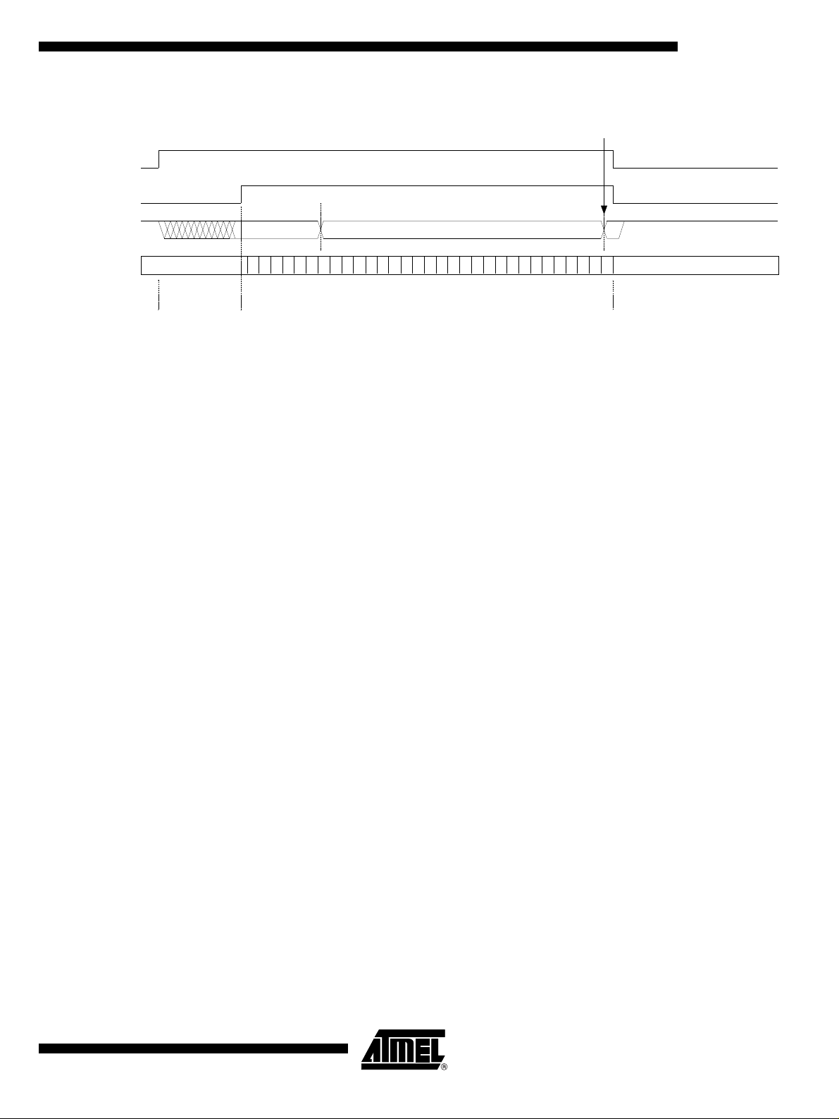
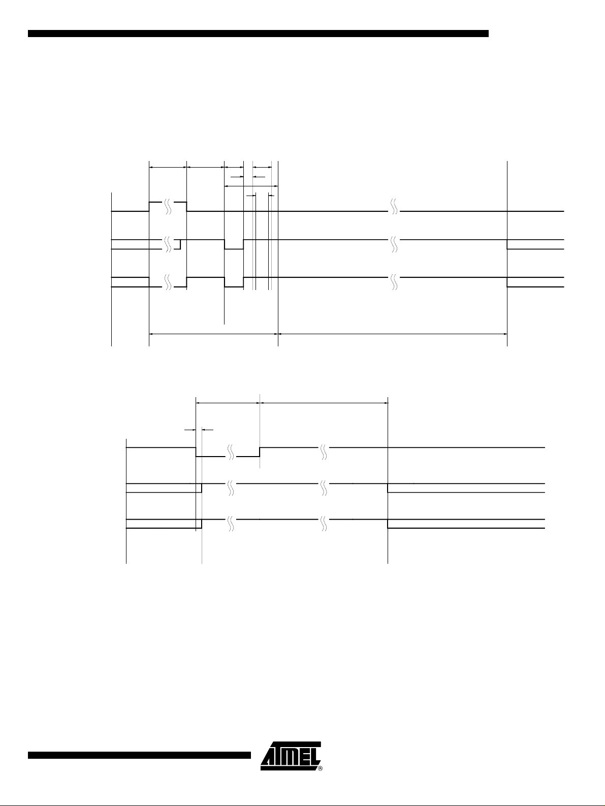
Figure 12. Timing Diagram for Failed Bit Check (condition: CV_Lim ³ Lim_max)
(Lim_min = 14, Lim_max = 24 )
Enable IC
U3745BM
Bit check failed (CV_Lim = Lim_max )
Bit check
Dem_out
Bit check Counter
0
Startup Mode
2345
1 7 36
6 245
1
Bitcheck Mode
789 111210
1/2 Bit
13 14 15 161718 19 21 22 23 24 0
20
Sleep Mode
Duration of the Bit Check If no transmitter signal is present during the bit check, the output of the demodulator
delivers random signals. The bit check is a statistical process and T
each check. Therefore, an average value for T
Characteristics”. T
baudrate range causes a lower value for T
depends on the selected baud rate range and on T
Bitcheck
Bitcheck
is given in the section “Electrical
Bitcheck
resulting in lower current consumption
Bitcheck
varies for
. A higher
Clk
in polling mode.
In the presence of a valid transmitter signal, T
that signal, f
thereby results in a longer period for T
preburst T
and the count of the checked bits, N
Sig
Bitcheck
Preburst
.
requiring a higher value for the transmitter
Receiving Mode If the bit check has been successful for all bits specified by N
is dependant on the frequency of
Bitcheck
. A higher value for N
Bitcheck
Bitcheck
, the receiver
Bitcheck
switches to receiving mode. According to Figure 9, the internal data signal is switched to
pin DATA in that case. A connected microcontroller can be woken up by the negative
edge at pin DATA. The receiver stays in that condition until it is switched back to polling
mode explicitly.
Digital Signal Processing The data from the demodulator (Dem_out) is digitally processed in different ways and as
a result converted into the output signal data. This processing depends on the selected
baud rate range (BR_Range). Figure 13 illustrates how Dem_out is synchronized by the
extended clock cycle T
change its state only after T
signal as a result is always an integral multiple of T
. This clock is also used for the bit check counter. Data can
XClk
elapsed. The edge-to-edge time period tee of the Data
XClk
XClk
.
The minimum time period between two edges of the data signal is limited to
³ T
t
ee
DATA_min
. This implies an efficient suppression of spikes at the DATA output. At the
same time, it limits the maximum frequency of edges at DATA. This eases the interrupt
handling of a connected microcontroller. T
ceding edge-to-edge time interval t
as illustrated in Figure 14. If tee is in between the
ee
DATA_min
is to some extent affected by the pre-
specified bit check limits, the following level is frozen for the time period
T
DATA_min
= tmin1, in case of tee being outside that bit check limits T
DATA_min
=tmin2 is the
relevant stable time period.
The maximum time period for DATA to be low is limited to T
DATA_L_max
. This function
ensures a finite response time during programming or switching off the receiver via pin
DATA. T
DATA_L_max
is thereby longer than the maximum time period indicated by the
transmitter data stream. Figure 15 gives an example where Dem_out remains low after
the receiver has switched to receiving mode.
15
4663A–RKE–06/03
Page 16
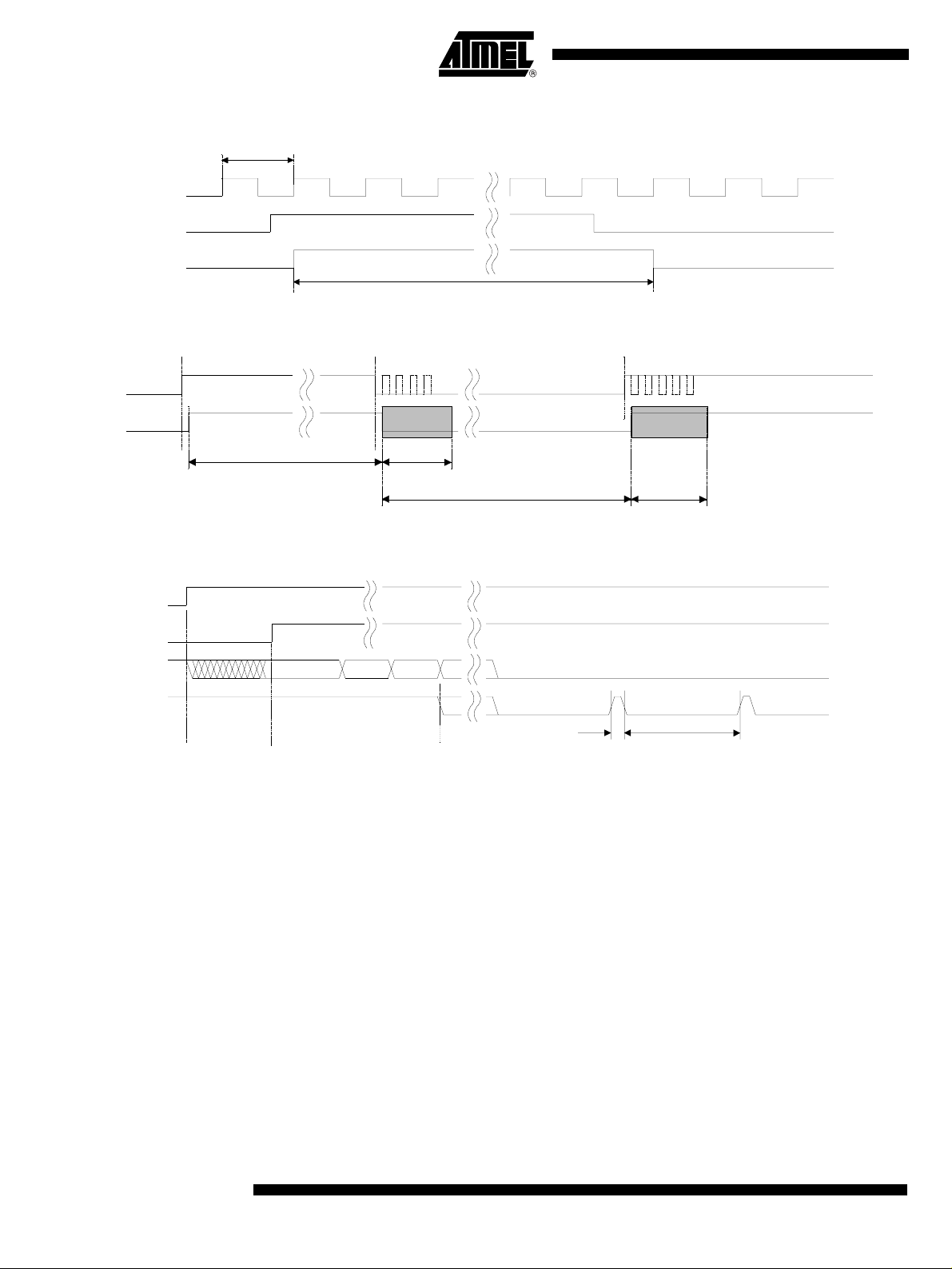
Figure 13. Synchronization of the Demodulator Output
T
XClk
Clock Bit check
counter
Dem_out
DATA
t
ee
Figure 14. Debouncing of the Demodulator Output
Dem_out
DATA
Lim_min £ CV_Lim < Lim_max
t
ee
tmin1
CV_Lim < Lim_min or CV_Lim ³ Lim_max
t
ee
Figure 15. Steady L State Limited DATA Output Pattern after Transmission
Enable IC
Bit check
Dem_out
DATA
Sleep Mode
Bit check Mode
Receiving Mode
tmin2
tmin2
t
DATA_L_max
Switching the Receiver Back
to Sleep Mode
16
U3745BM
After the end of a data transmission, the receiver remains active and random noise
pulses appear at pin DATA. The edge-to-edge time period t
noise pulses is equal to or slightly higher than T
DATA_min
.
of the majority of these
ee
The receiver can be set back to polling mode via pin DATA or via pin ENABLE.
When using pin DATA, this pin must be pulled to Low for the period t1 by the connected
microcontroller. Figure 16 illustrates the timing of the OFF command (see also Figure
20). The minimum value of t1 depends on the BR_Range. The maximum value for t1 is
not limited but it is recommended not to exceed the specified value to prevent erasing
the reset marker. This item is explained in more detail in the section “Configuration of
the Receiver”. Setting the receiver to sleep mode via DATA is achieved by programming
bit 1 of the OPMODE register to 1. Only one sync pulse (t3) is issued.
The duration of the OFF command is determined by the sum of t1, t2 and t10. After the
OFF command, the sleep time T
elapses. Note that the capacitive load at Pin DATA
Sleep
is limited. The resulting time constant t together with an optional external pull-up resistor
may not be exceeded to ensure proper operation.
If the receiver is set to polling mode via pin ENABLE, an ‘L’ pulse (T
) must be issued
Doze
at that pin. Figure 17 illustrates the timing of that command. After the positive edge of
4663A–RKE–06/03
Page 17
U3745BM
this pulse, the sleep time T
Sleep
ENABLE is held to ‘L’. If the receiver is polled exclusively by a microcontroller, T
be programmed to 0 to enable a instantaneous response time. This command is the
faster option than via pin DATA at the cost of an additional connection to the
microcontroller.
Figure 16. Timing Diagram of the OFF Command Via Pin DATA
Out1 (mC)
DATA (U3745BM)
Serial bi-directional
data line
t1 t2 t3
X
X
Receiver
on
OFF Command
t4
t10
Bit 1
("1")
(Start bit)
t5
t7
elapses. The receiver remains in sleep mode as long as
can
Sleep
X
X
T
Sleep
Startup mode
Figure 17. Timing Diagram of the OFF Command Via Pin ENABLE
T
Sleep
ENABLE
DATA (U3745BM)
Serial bi-directional
data line
Configuration of the
Receiver
X
X
Receiver on
T
Doze
toff
The U3745BM receiver is configured via two 12-bit RAM registers called OPMODE and
LIMIT. The registers can be programmed by means of the bi-directional DATA port. If
the register contents have changed due to a voltage drop, this condition is indicated by a
certain output pattern called reset marker (RM). The receiver must be reprogrammed in
that case. After a power-on reset (POR), the registers are set to default mode. If the
receiver is operated in default mode, there is no need to program the registers.
Table 3 shows the structure of the registers. According to Table 2, bit 1 defines if the
receiver is set back to polling mode via the OFF command, (see section “Receiving
Mode”) or if it is programmed. Bit 2 represents the register address. It selects the appropriate register to be programmed.
X
X
Startup mode
4663A–RKE–06/03
17
Page 18
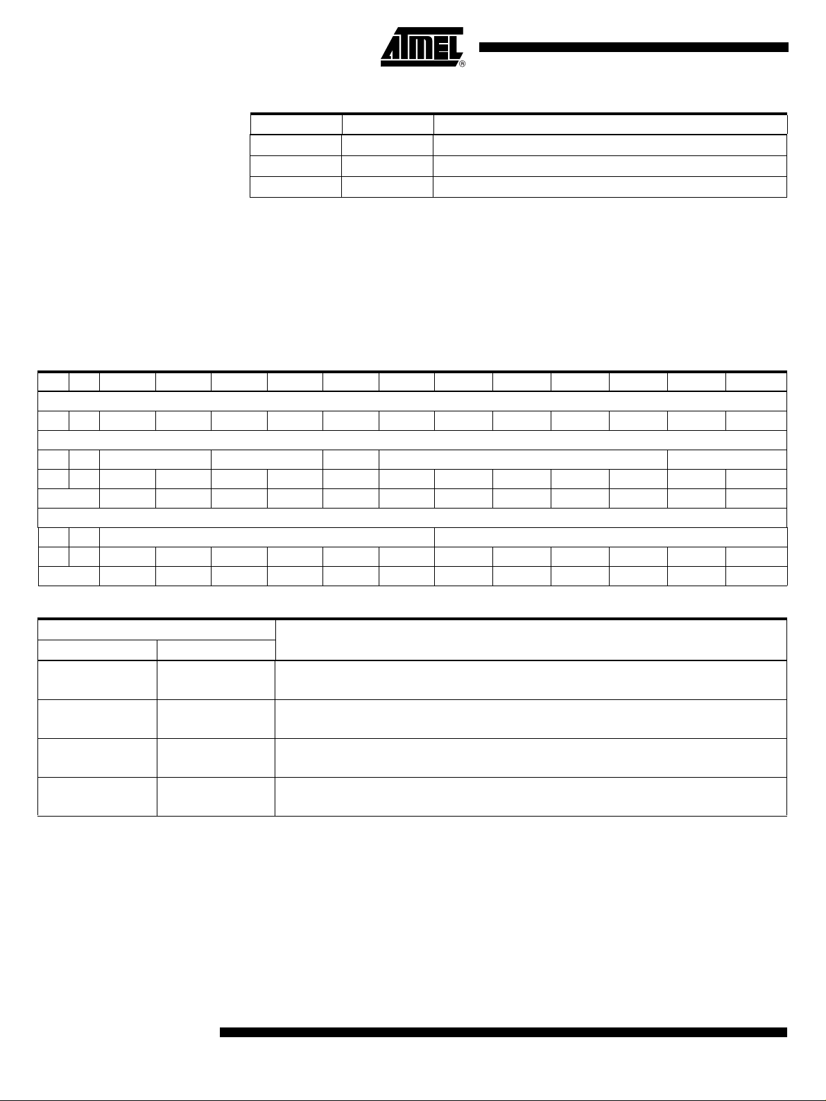
Table 2. Effect of Bit 1 and Bit 2 in Programming the Registers
Bit 1 Bit 2 Action
1 x The receiver is set back to polling mode (OFF command)
0 1 The OPMODE register is programmed
0 0 The LIMIT register is programmed
Table 4 and the following illustrate the effect of the individual configuration words. The
default configuration is highlighted for each word.
BR_Range sets the appropriate baud rate range. At the same time it defines XLim. XLim
is used to define the bit check limits T
Lim_min
and T
as shown in Table 4.
Lim_max
POUT can be used to control the sensitivity of the receiver. In that application, POUT is
set to 1 to reduce the sensitivity. This implies that the receiver operates with full sensitivity after a POR.
Table 3. Effect of the Configuration Words within the Registers
Bit1 Bit2 Bit2 Bit4 Bit5 Bit6 Bit7 Bit8 Bit9 Bit10 Bit11 Bit12 Bit13 Bit14
OFF Command
1
OPMODE Register
0 1 BR_Range N
0 1 Baud1 Baud0 BitChk1 BitChk0 POUT Sleep4 Sleep3 Sleep2 Sleep1 Sleep0 X
(Default)00100010110 0
LIMIT Register
0 0 Lim_min Lim_max
0 0 Lim_min5 Lim_min4 Lim_min3 Lim_min2 Lim_min1 Lim_min0 Lim_max5 Lim_max4 Lim_max3 Lim_max2 Lim_max1 Lim_max0
(Default)00111001100 0
Bitcheck
V
POUT
Sleep XSleep
Sleep StdXSleep Temp
Table 4. Effect of the Configuration Word BR_Range
BR_Range
Baudrate Range/Extension Factor for Bit Check Limits (XLim)Baud1 Baud0
0 0 BR_Range0 (application USA/Europe: BR_Range0 = 1.0 kBaud to 1.8 kBaud) (Default)
XLim = 8 (Default)
0 1 BR_Range1 (application USA/Europe: BR_Range1 = 1.8 kBaud to 3.2 kBaud)
XLim = 4
1 0 BR_Range2 (application USA/Europe: BR_Range2 = 3.2 kBaud to 5.6 kBaud)
XLim = 2
1 1 BR_Range3 (Application USA/Europe: BR_Range3 = 5.6 kBaud to 10 kBaud)
XLim = 1
18
U3745BM
4663A–RKE–06/03
Page 19

U3745BM
Table 5. Effect of the Configuration Word N
N
Bitcheck
Bitcheck
Number of Bits to be CheckedBitChk1 BitChk0
00 0
01 3
1 0 6 (Default)
11 9
Table 6. Effect of the Configuration Bit VPOUT
VPOUT Level of the Multi-purpose Output Port POUT
POUT
00 (Default)
11
Table 7. Effect of the Configuration Word Sleep
Sleep
Start Value for Sleep Counter (T
00000 0 (Receiver is continuously polling until a valid signal occurs)
00001 1 (T
» 2ms for XSleep = 1 in US-/European applications)
Sleep
00010 2
00011 3
.
.
.
01011 11 (USA: T
.
.
.
.
.
.
.
.
.
.
.
.
.
.
.
.
.
.
.
.
.
.
.
.
= 22.96 ms, Europe: T
Sleep
.
.
.
11101 29
11110 30
11111 31 (Permanent sleep mode)
= Sleep ´ Xsleep ´ 1024 ´ T
Sleep
.
.
.
= 23.31 ms) (Default)
Sleep
.
.
.
Clk
)Sleep4 Sleep3 Sleep2 Sleep1 Sleep0
Table 8. Effect of the Configuration Word XSleep
XSleep
Std
0 0 1 (Default)
0 1 8 (XSleep is reset to 1 if bit check fails once)
1 0 8 (XSleep is set permanently)
1 1 8 (XSleep is set permanently)
4663A–RKE–06/03
XSleep
Temp
Extension Factor for Sleep Time (T
= Sleep ´ Xsleep ´ 1024 ´ T
Sleep
Clk
)XSleep
19
Page 20

Table 9. Effect of the Configuration Word Lim_min
Lim_min Lower Limit Value for Bit Check
Lim_min < 10 is not applicable (T
= Lim_min ´ XLim ´ T
Lim_min
001010 10
001011 11
001100 12
001101 13
001110 14 (Default)
(USA: T
.
.
.
.
.
.
.
.
.
.
.
.
.
.
.
.
.
.
= 228 µs, Europe: T
Lim_min
111101 61
111110 62
111111 63
Table 10. Effect of the Configuration Word Lim_max
Lim_max Upper Limit Value for Bit Check
Lim_max < 12 is not applicable (T
001100 12
001101 13
001110 14
.
.
.
.
.
.
.
.
.
.
.
.
.
.
.
.
.
.
011000 24 (Default)
(USA: T
.
.
.
.
.
.
.
.
.
.
.
.
.
.
.
.
.
.
111101 61
111110 62
111111 63
= (Lim_max - 1) ´ XLim ´ T
Lim_max
= 375 µs, Europe: T
Lim_max
Lim_min
Lim_max
)
Clk
= 232 µs)
)
Clk
= 381 µs)
Conservation of the Register
Information
20
U3745BM
The U3745BM has an integrated power-on reset and brown-out detection circuitry to
provide a mechanism to preserve the RAM register information.
According to Figure 18, a power-on reset (POR) is generated if the supply voltage V
drops below the threshold voltage V
the configuration registers in that condition. Once V
celed after the minimum reset period t
. The default parameters are programmed into
ThReset
. A POR is also generated when the supply
Rst
exceeds V
S
, the POR is can-
ThReset
voltage of the receiver is turned on.
To indicate that condition, the receiver displays a reset marker (RM) at pin DATA after a
reset. The RM is represented by the fixed frequency f
at a 50% duty cycle. RM can be
RM
canceled via an ‘L’ pulse t1 at pin DATA. The RM implies the following characteristics:
•f
is lower than the lowest feasible frequency of a data signal. By this means, RM
RM
cannot be misinterpreted by the connected microcontroller.
4663A–RKE–06/03
S
Page 21
• If the receiver is set back to polling mode via pin DATA, RM cannot be canceled by
accident if t1 is applied according to the proposal in the section “Programming the
Configuration Registers”.
By means of that mechanism, the receiver cannot lose its register information without
communicating that condition via the reset marker RM.
Figure 18. Generation of the Power-on Reset
V
S
POR
t
Rst
DATA (U3745BM)
X
V
ThRes et
U3745BM
1 / f
Figure 19. Timing of the Register Programming
t1 t2 t3
Out1 (mC)
DATA (U3745BM)
Serial bi-directional
data line
Programming the
Configuration Register
X
X
Receiver
on
(Start bit) (Register
The configuration registers are programmed serially via the bi-directional data line
according to Figure 19 and Figure 20.
t4
Bit 1
("0")
T
t5
t6
t7
Bit 2
("1")
select)
Programming Frame
Bit 13
("0")
(Poll8) (Poll8R)
Bit 14
("1")
Sleep
t9
t8
X
X
Startup
mode
4663A–RKE–06/03
21
Page 22

Figure 20. One-wire Connection to a Microcontroller
U3745BM
Internal pull-up
resistor
DATA (U3745BM)
Bi-directional
data line
DATA I/O
mC
Out 1 (mC)
To start programming, the serial data line DATA is pulled to ‘L’ for the time period t1 by
the microcontroller. When DATA has been released, the receiver becomes the master
device. When the programming delay period t2 has elapsed, it emits 14 subsequent
synchronization pulses with the pulse length t3. After each of these pulses, a programming window occurs. The delay until the program window starts is determined by t4, the
duration is defined by t5. Within the programming window, the individual bits are set. If
the microcontroller pulls down pin DATA for the time period t7 during t5, the according
bit is set to ‘0’. If no programming pulse t7 is issued, this bit is set to ‘1’. All 14 bits are
subsequently programmed in this way. The time frame to program a bit is defined by t6.
Bit 14 is followed by the equivalent time window t9. During this window, the equivalent
acknowledge pulse t8 (E_Ack) occurs if the mode word just programmed is equivalent to
the mode word that was already stored in that register. E_Ack should be used to verify
that the mode word was correctly transferred to the register. The register must be programmed twice in that case.
Programming of a register is possible both during sleep and active mode of the receiver.
During programming, the LNA, LO, lowpass filter, IF-amplifier and the demodulator are
disabled.
The programming start pulse t1 initiates the programming of the configuration registers.
If bit 1 is set to ‘1’, it represents the OFF command to set the receiver back to polling
mode at the same time. For the length of the programming start pulse t1, the following
convention should be considered:
´ T
• t1(min) < t1 < 1535
: [t1(min) is the minimum specified value for the relevant
Clk
BR_Range]
Programming (respectively OFF command) is initiated if the receiver is not in reset
mode. If the receiver is in reset mode, programming (respectively Off command) is not
initiated, and the reset marker RM is still present at pin DATA.
This period is generally used to switch the receiver to polling mode. In a reset condition,
RM is not canceled by accident.
t1 > 5632 ´ T
•
Clk
Programming (respectively OFF command) is initiated in any case. RM is cancelled if
present. This period is used if the connected microcontroller detected RM. If a configuration register is programmed, this time period for t1 can generally be used.
Note that the capacitive load at pin DATA is limited. The resulting time constant t
together with an optional external pull-up resistor may not be exceeded to ensure proper
operation.
22
U3745BM
4663A–RKE–06/03
Page 23

U3745BM
Absolute Maximum Ratings
Parameters Symbol Min. Max. Unit
Supply voltage V
Power dissipation P
Junction temperature T
Storage temperature T
Ambient temperature T
Maximum input level, input matched to 50
W P
S
tot
j
stg
amb
in_max
-55 +125 °C
-40 +85 °C
Thermal Resistance
Parameters Symbol Value Unit
Junction ambient R
thJA
100 K/W
Electrical Characteristics
6V
450 mW
150 °C
10 dBm
All parameters refer to GND, VS = 5 V, T
possible operating range refer to different circuit conditions: V
= 25°C, f0 = 433.92 MHz and f0= 315 MHz, unless otherwise specified. The
amb
= 4.5 V to 5.5 V, T
S
= -40°C to +85°C
amb
Parameters Test Conditions Symbol Min. Typ. Max. Unit
Current consumption
Sleep mode
(XTO and polling logic active)
IC active
(startup-, bit check-, receiving mode)
IS
IS
off
on
190 350 µA
7.0 8.6 mA
Pin DATA = H
LNA Mixer
Third-order intercept point
LO spurious emission at RF
In
LNA/mixer/IF amplifier
input matched according to Figure 4
Input matched according to Figure 4,
required according to I-ETS 300220
IIP3 -28 dBm
IS
LORF
-73 -57 dBm
Noise figure LNA and mixer (DSB) Input matching according to Figure 4 NF 7 dB
LNA_IN input impedance
1 dB compression point (LNA, mixer,
IF amplifier)
Maximum input level
at 433.92 MHz
at 315 MHz
Input matched according to Figure 4,
referred to RF
Input matched according to Figure 4,
BER
£ 10
in
-3
,
Zi
IP
P
LNA_IN
1db
in_max
1.0 || 1.56
1.3 || 1.0
-40 dBm
-23 dBm
kW || pF
k
W || pF
ASK mode
Local Oscillator
Operating frequency range VCO f
VCO
309 439 MHz
For best LO noise
(design parameter)
Loop bandwidth of the PLL
R1 = 820
W
B
Loop
100 kHz
C9 = 4.7 nF
C10 = 1 nF
The capacitive load at pin LF is limited
Capacitive load at Pin LF
if bit check is used. The limitation
C
LF_tot
10 nF
therefore also applies to self polling.
4663A–RKE–06/03
23
Page 24

Electrical Characteristics (Continued)
All parameters refer to GND, VS = 5 V, T
possible operating range refer to different circuit conditions: V
= 25°C, f0 = 433.92 MHz and f0= 315 MHz, unless otherwise specified. The
amb
= 4.5 V to 5.5 V, T
S
= -40°C to +85°C
amb
Parameters Test Conditions Symbol Min. Typ. Max. Unit
XTO crystal frequency,
appropriate load capacitance must be
XTO operating frequency
Series resonance resistor of the
crystal
Static capacitance at Pin XT0 C
connected to XTAL
6.764375 MHz
4.90625 MHz
f
= 6.764 MHz
XTO
4.906 MHz
f
R
XTO
XT0
6.764375
-50 ppm
4.90625
-50 ppm
S
6.764375
4.90625
6.764375
+50 ppm
4.90625
+50 ppm
150
220
MHz
MHz
6.5 pF
Analog Signal Processing
Input matched according to figure 6
Input sensitivity ASK 600-kHz IF filter
ASK (level of carrier)
BER
f
= 433.92 MHz/315 MHz
in
T = 25
f
IF
£ 10
°C, V
= 1 MHz
-3
, B = 600 kHz
= 5 V
S
P
Ref_ASK
BR_Range0 -106 -110 -113.5 dBm
BR_Range1 -104.5 -108.5 -112 dBm
BR_Range2 -104 -108 -111.5 dBm
BR_Range3 -102 -106 -109.5 dBm
600-kHz version
Sensitivity variation ASK for full
operating range including IF filter
compared to T
=25°C, VS = 5 V
amb
S/N ratio to suppress inband noise
signals
Dynamic range RSSI ampl. DR
= 433.92 MHz/315 MHz
f
in
f
= 0.81 MHz to 1.19 MHz
IF
f
= 0.75 MHz to 1.25 MHz
IF
= P
P
ASK
Ref_ASK
+ DP
Ref
ASK mode
DP
SNR
Ref
ASK
RSSI
+3
+5
dB
dB
11 dB
60 dB
W
W
Lower cut-off frequency of the data
filter
Recommended CDEM for best
performance
Maximum edge-to-edge time period of
the input data signal for full sensitivity
Minimum edge-to-edge time period of
the input data signal for full sensitivity
24
U3745BM
f
cu_DF
------------ ------------- ------------- ----------- --------=
p´ 30kW´ CDEM´
2
CDEM = 33 nF
ASK mode
BR_Range0 (Default)
BR_Range1
BR_Range2
BR_Range3
BR_Range0 (Default)
BR_Range1
BR_Range2
BR_Range3
BR_Range0 (Default)
BR_Range1
BR_Range2
BR_Range3
1
f
cu_DF
CDEM
t
ee_sig
t
ee_sig
0.11 0.16 0.20 kHz
39
22
12
8.2
1000
560
320
180
270
156
89
50
4663A–RKE–06/03
nF
nF
nF
nF
µs
µs
µs
µs
µs
µs
µs
µs
Page 25

Electrical Characteristics (Continued)
U3745BM
All parameters refer to GND, VS = 5 V, T
possible operating range refer to different circuit conditions: V
= 25°C, f0 = 433.92 MHz and f0= 315 MHz, unless otherwise specified. The
amb
= 4.5 V to 5.5 V, T
S
= -40°C to +85°C
amb
Parameters Test Conditions Symbol Min. Typ. Max. Unit
Threshold voltage for reset V
ThRESET
1.95 2.8 3.75 V
Digital Ports
Data output
- Saturation voltage LOW
- Internal pull-up resistor
- Maximum time constant
- Maximum capacitive load
I
= 1 mA
ol
t = C
(R
//R
L
pup
Ext
)
without ext. pull-up resistor
R
= 5 kW
ext
V
OI
R
Pup
39
t
C
L
C
L
0.08
50
0.3
61
2.5
41
540
kW
µs
pF
pF
POUT output
- Saturation voltage LOW
- Saturation voltage HIGH
I
POUT
I
POUT
= 1 mA
= -1 mA
V
Ol
V
Oh
VS-0.3V
0.08
VS-0.14V
0.3 V
ASK input
- High-level input voltage ASK V
Ih
0.8 ´ V
S
ENABLE input
- Low-level input voltage
- High-level input voltage
Idle mode
Active mode
V
Il
V
Ih
0.8 ´ V
S
0.2 ´ V
S
MODE input
- Low-level input voltage
- High-level input voltage
TEST input
- Low-level input voltage
Division factor = 10
Division factor = 14
Test input must always be set to LOW
V
Il
V
Ih
V
Il
0.8 ´ V
S
0.2 ´ V
0.2 ´ V
S
S
V
V
V
V
V
V
V
V
Electrical Characteristics
All parameters refer to GND, VS = 5 V, T
possible operating range refer to different circuit conditions: V
Parameter Test Condition Symbol
Basic Clock Cycle of the Digital Circuitry
Basic clock
cycle
Extended
basic clock
cycle
Polling Mode
Sleep time
Start-up time
MODE = 0 (USA)
MODE = 1
(Europe)
BR_Range0
BR_Range1
BR_Range2
BR_Range3
Sleep and XSleep
are defined in the
OPMODE register
BR_Range0
BR_Range1
BR_Range2
BR_Range3
T
T
T
T
Startup
Clk
XClk
Sleep
= 25°C, f0 = 433.92 MHz and f0= 315 MHz, unless otherwise specified. The
amb
6.76438-Mhz Osc.
(Mode 1)
2.0697
16.6
8.3
4.1
2.1
Sleep ´
´
X
Sleep
1024
´
2.0697
1855
1061
1061
663
= 4.5 V to 5.5 V, T
S
4.90625-Mhz Osc.
(Mode 0) Variable Oscillator
2.0383 1/(f
16.3
8.2
4.1
2.0
´
Sleep
´
X
Sleep
1024
´
2.0383
1827
1045
1045
653
= -40°C to +85°C
amb
1/(f
8
4 ´ T
2 ´T
1 ´ T
Sleep
X
1024
896.5
512.5
512.5
320.5
´ T
XTO
XTO
´ T
Sleep
Clk
´ T
Clk
/10)
/14)
Clk
Clk
Clk
´
´
UnitMin. Typ. Max. Min. Typ. Max. Min. Typ. Max.
µs
µs
µs
µs
µs
µs
ms
Clk
µs
µs
µs
µs
4663A–RKE–06/03
25
Page 26

Electrical Characteristics
All parameters refer to GND, VS = 5 V, T
= 25°C, f0 = 433.92 MHz and f0= 315 MHz, unless otherwise specified. The
amb
possible operating range refer to different circuit conditions: V
6.76438-Mhz Osc.
(Mode 1)
Parameter Test Condition Symbol
Average bit check
time while polling
BR_Range0
BR_Range1
BR_Range2
Time for Bit
check
BR_Range3
Bit check time for a
valid input signal
f
Sig
N
= 0
Bitcheck
= 3
N
Bitcheck
N
= 6
Bitcheck
= 9
N
Bitcheck
Receiving Mode
Intermediate
frequency
MODE=0 (USA)
MODE=1 (Europe)
BR_Range0
Baud rate
range
BR_Range1
BR_Range2
BR_Range3
Minimum time
period
between
edges at
Pin DATA
(Figure 14)
Maximum low
period at
DATA
(Figure 15)
BR_Range0
BR_Range1
BR_Range2
BR_Range3
BR_Range0
BR_Range1
BR_Range2
BR_Range3
OFF
command at
Pin ENABLE
(Figure 17)
Configuration of the Receiver
Frequency of
the reset
marker
(Figure 18)
T
Bitcheck
T
Bitcheck
f
IF
BR_Range
T
DATA_m in
tmin1
tmin2
tmin1
tmin2
tmin1
tmin2
tmin1
tmin2
T
DATA_L_max
t
Doze
f
RM
3/f
6/f
9/f
1.0
1.8
3.2
5.6
3.1 3.05 1.5 ´
0.45
0.24
0.14
0.14
Sig
Sig
Sig
3.5/f
6.5/f
9.5/f
1.0
10.0
149
182
75
91
37.3
45.5
18.6
22.8
2169
1085
542
271
117.9 119.8 Hz
= 4.5 V to 5.5 V, T
S
4.90625-Mhz Osc.
(Mode 0) Variable Oscillator
0.47
0.26
0.16
0.15
3/f
Sig
Sig
6/f
Sig
Sig
9/f
Sig
Sig
1.0
1.8
3.2
5.6
1.0
1.8
3.2
5.6
147
179
73
90
36.7
44.8
18.3
22.4
2136
1068
534
267
= -40°C to +85°C
amb
3.5/f
Sig
6.5/f
Sig
9.5/f
Sig
1.8
3.2
5.6
10.0
T
Clk
T
XClk
f
´ 64 / 314
XTO
´ 64 / 432.92
f
XTO
BR_Range0
BR_Range1
´ 2 ms / T
´ 2 ms / T
BR_Range2 ´ 2 ms / T
BR_Range3 ´ 2 ms / T
9
´ T
XClk
11 ´ T
XCl
9 ´ T
XClk
11 ´ T
XClk
9 ´ T
XClk
11 ´ T
XClk
9 ´ T
XClk
11 ´ T
XClk
´ T
131
XClk
131 ´ T
XClk
131 ´ T
XClk
131 ´ T
XClk
1
------------- ------------- ------
´
4096 T
CLK
3.5/f
6.5/f
9.5/f
Clk
Clk
Clk
Clk
UnitMin. Typ. Max. Min. Typ. Max. Min. Typ. Max.
ms
ms
ms
ms
ms
ms
Sig
ms
Sig
Sig
ms
MHz
MHz
kBaud
kBaud
kBaud
kBaud
µs
µs
µs
µs
µs
µs
µs
µs
µs
µs
µs
µs
µs
26
U3745BM
4663A–RKE–06/03
Page 27

Electrical Characteristics
U3745BM
All parameters refer to GND, VS = 5 V, T
= 25°C, f0 = 433.92 MHz and f0= 315 MHz, unless otherwise specified. The
amb
possible operating range refer to different circuit conditions: V
6.76438-Mhz Osc.
(Mode 1)
Parameter Test Condition Symbol
Programming
start pulse
(Figure 16,
Figure 19)
Programming
delay period
(Figure 16,
Figure 19)
Synchroni-
zation pulse
(Figure 16,
Figure 19)
Delay until the
program
window starts
(Figure 16,
Figure 19)
Programming
window
(Figure 16,
Figure 19)
Time frame
of a bit
(Figure 19)
Programming
pulse (Figure
16, Figure 19)
Equivalent
acknowledge
pulse: E_Ack
(Figure 19)
Equivalent
time window
(Figure 19)
OFF-bit
programming
window
(Figure 16)
BR_Range0
BR_Range1
BR_Range2
BR_Range3
after POR
t1 2188
1104
561
290
3176
3176
3176
3176
11656
t2 795 798 783 786
t3 265 261
t4 131 129 63.5
t5 530 522 256
t6 1060 1044 512
t7 133 529 131 521 64
t8 265 261 128
t9 534 526 258
t10 930 916 449.5
= 4.5 V to 5.5 V, T
S
4.90625-Mhz Osc.
(Mode 0) Variable Oscillator
2155
1087
553
286
11479
= -40°C to +85°C
amb
3128
3128
3128
3128
1057
T
Clk
533 ´
T
Clk
271 ´
T
Clk
140 ´
T
Clk
5632 ´
T
Clk
384.5 ´
T
Clk
´ T
Clk
´
128 ´ T
´ T
´ T
´ T
´ T
´ T
´ T
Clk
Clk
Clk
Clk
Clk
Clk
Clk
1535 ´
T
Clk
1535 ´
T
Clk
1535 ´
T
Clk
1535 ´
T
Clk
385.5 ´
T
Clk
256 ´
T
Clk
UnitMin. Typ. Max. Min. Typ. Max. Min. Typ. Max.
µs
µs
µs
µs
µs
µs
µs
µs
µs
µs
4663A–RKE–06/03
27
Page 28

Ordering Information
Extended Type Number Package Remarks
U3745BM-MFL SO20
U3745BM-MFLG3 SO20
Tube
Taped and reeled
Package Information
Package SO20
Dimensions in mm
0.4
1.27
20 11
12.95
12.70
11.43
0.25
0.10
2.35
technical drawings
according to DIN
specifications
9.15
8.65
7.5
7.3
0.25
10.50
10.20
28
110
U3745BM
4663A–RKE–06/03
Page 29

Atmel Headquarters Atmel Operations
Corporate Headquarters
2325 Orchard Parkway
San Jose, CA 95131
TEL 1(408) 441-0311
FAX 1(408) 487-2600
Europe
Atmel Sarl
Route des Arsenaux 41
Case Postale 80
CH-1705 Fribourg
Switzerland
TEL (41) 26-426-5555
FAX (41) 26-426-5500
Asia
Room 1219
Chinachem Golden Plaza
77 Mody Road Tsimhatsui
East Kowloon
Hong Kong
TEL (852) 2721-9778
FAX (852) 2722-1369
Japan
9F, Tonetsu Shinkawa Bldg.
1-24-8 Shinkawa
Chuo-ku, Tokyo 104-0033
Japan
TEL (81) 3-3523-3551
FAX (81) 3-3523-7581
Memory
2325 Orchard Parkway
San Jose, CA 95131
TEL 1(408) 441-0311
FAX 1(408) 436-4314
Microcontrollers
2325 Orchard Parkway
San Jose, CA 95131
TEL 1(408) 441-0311
FAX 1(408) 436-4314
La Chantrerie
BP 70602
44306 Nantes Cedex 3, France
TEL (33) 2-40-18-18-18
FAX (33) 2-40-18-19-60
ASIC/ASSP/Smart Cards
Zone Industrielle
13106 Rousset Cedex, France
TEL (33) 4-42-53-60-00
FAX (33) 4-42-53-60-01
1150 East Cheyenne Mtn. Blvd.
Colorado Springs, CO 80906
TEL 1(719) 576-3300
FAX 1(719) 540-1759
Scottish Enterprise Technology Park
Maxwell Building
East Kilbride G75 0QR, Scotland
TEL (44) 1355-803-000
FAX (44) 1355-242-743
RF/Automotive
Theresienstrasse 2
Postfach 3535
74025 Heilbronn, Germany
TEL (49) 71-31-67-0
FAX (49) 71-31-67-2340
1150 East Cheyenne Mtn. Blvd.
Colorado Springs, CO 80906
TEL 1(719) 576-3300
FAX 1(719) 540-1759
Biometrics/Imaging/Hi-Rel MPU/
High Speed Converters/RF Datacom
Avenue de Rochepleine
BP 123
38521 Saint-Egreve Cedex, France
TEL (33) 4-76-58-30-00
FAX (33) 4-76-58-34-80
e-mail
literature@atmel.com
Web Site
http://www.atmel.com
© Atmel Corporation 2003.
Atmel Corporation makes no warranty for the use of its products, other than those expressly contained in the Company’s standard warranty
which is detailed in Atmel’s Terms and Conditions located on the Company’s web site. The Company assumes no responsibility for any errors
which may appear in this document, reserves the right to change devices or specifications detailed herein at any time without notice, and does
not make any commitment to update the information contained herein. No licenses to patents or other intellectual property of Atmel are granted
by the Company in connection with the sale of Atmel products, expressly or by implication. Atmel’s products are not authorized for use as critical
components in life support devices or systems.
Atmel® is the registered trademark of Atmel.
Other terms and product names may be the trademarks of others.
Printed on recycled paper.
4663A–RKE–06/03
xM
 Loading...