

Page 1
Features
• Very High Transmitting Frequency Accuracy Compared to SAW Solutions
(Enables Receivers at Lower Bandwidth than with SAW Resonators)
• Lower Cost than the Usual Discrete Solutions Using SAW and Transistors
• Supply Voltage 2.2 V to 4.0 V in the Temperature Range of -40°C to 85°C
• XTO Output for Clocking the Microcontroller, Thereby Together with the ATAR090 or
ATAR890 Results in the Optimum System Cost-effectiveness
• One-chip Solution with Minimum External Circuitry
• Very Small SSO16 Package, Pitch 0.635, 150 mil
• “Single-ended Open-collector” Output (Same Antennas Can Be Used as in Discrete
Solutions, Simpler Adaptation of Magnetic Loop Antennas)
• ESD Protection According to MIL-STD.883 (4 KV HBM) Except Pins XTO1/ 2,
ANT and LF
UHF ASK
Transmitter
Electrostatic sensitive device.
Observe precautions for handling.
Description
The U2745B is a PLL transmitter IC which has been especially developed for the
demands of RF low-cost data transmission systems at data rates up to 20 kBaud.
The transmitting frequency range is 310 MHz to 440 MHz. It can be used in ASK systems. The main applications of the U2745B are in the areas of outside temperature
metering, socket control, garage door opener, consumption metering, light/fan or aircondition control, jalousies, wireless keyboard and various other consumer market
applications.
U2745B
Rev. 4734A–RKE–11/03
Page 2
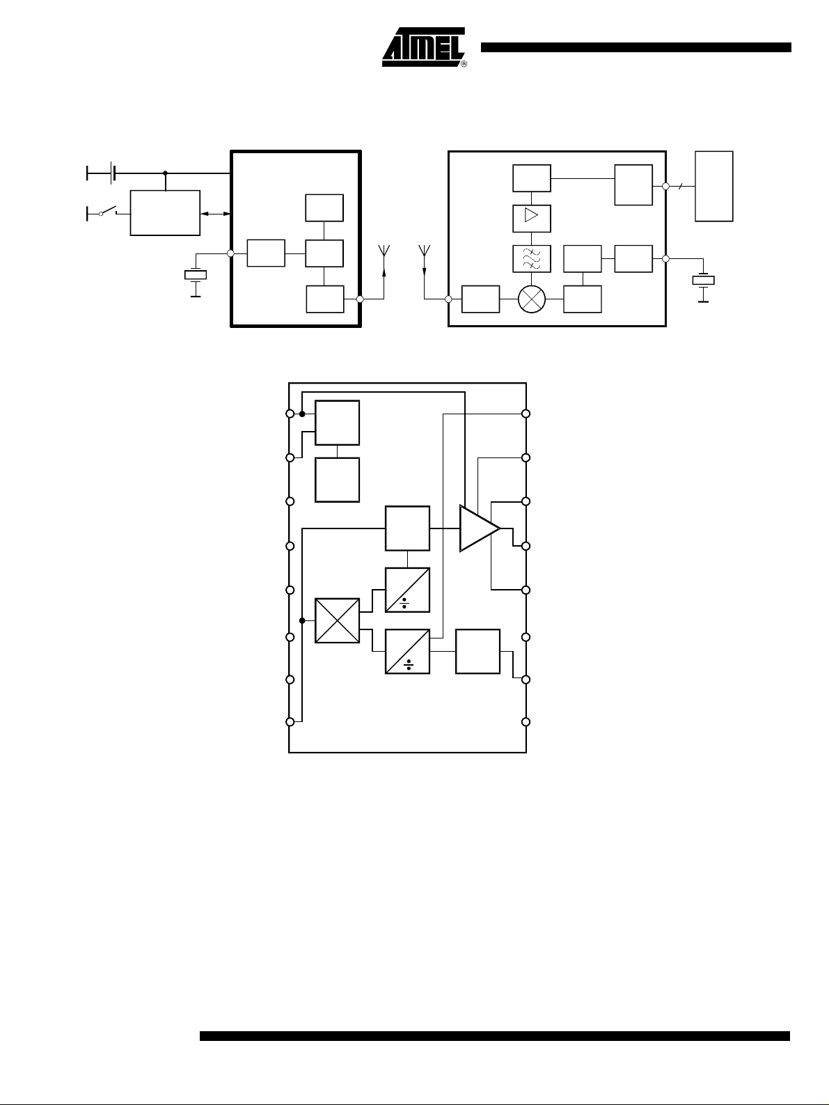
Figure 1. System Block Diagram
1 Li cell
Keys
Encoder
ATARx9x
Remote control transmitter
UHF ASK
U2745B
XTO
PLL
VCO
Antenna Antenna
U3745BM
UHF ASK
Remote control receiver
Demod.
IF Amp
PLL XTO
Control
1...3
controller
Micro-
Figure 2. Block Diagram
ASK
EN
VCC
CLK
GND
LFVCC
LFGND
Power
amp.
OR
Power
up
VCO
f
f
LNA VCO
GND
PWRSET
PWRVCC
PA
ANT
PWRGND1
64
PWRGND2
XTO
n
XTO1
LF
NC
U2745B
2
U2745B
4734A–RKE–11/03
Page 3
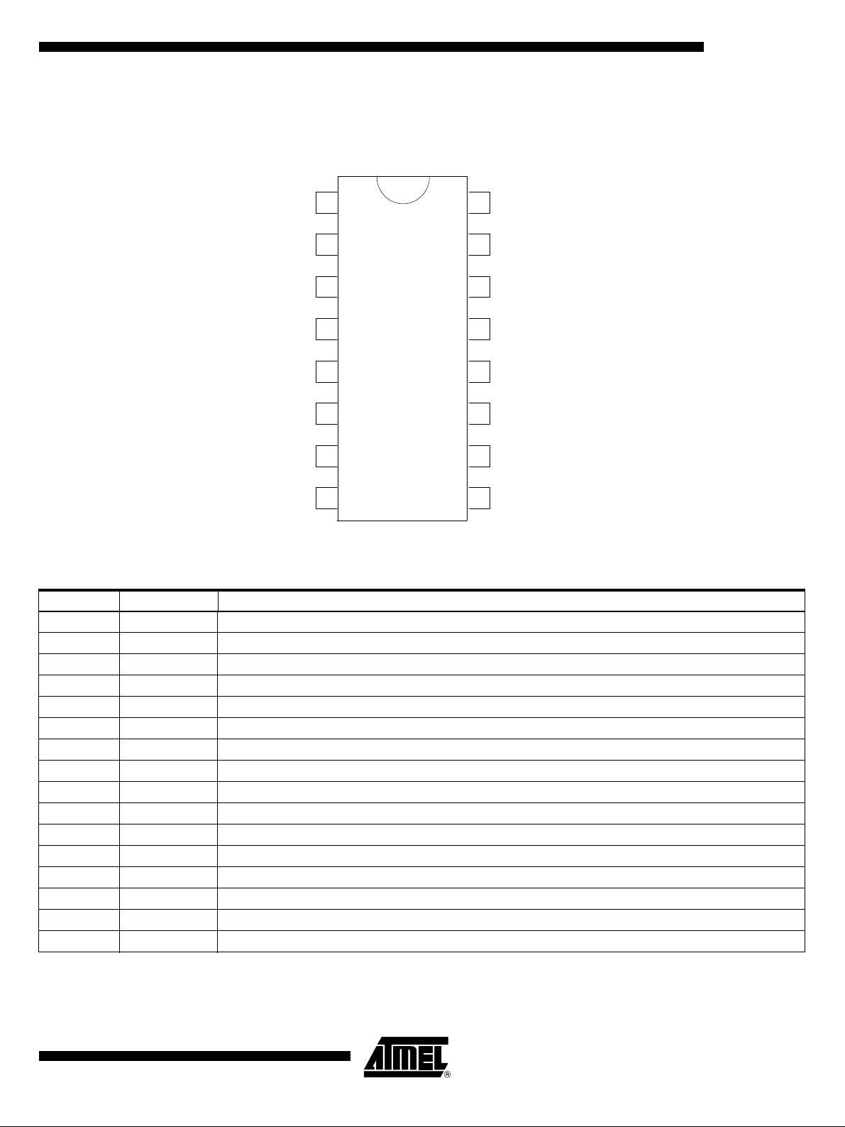
Pin Configuration
Figure 3. Pinning SSO16
ASK
U2745B
1
16
GND
EN
VCC
3
CLK
5
GND
LFVCC
LFGND
8
LF
Pin Description
Pin Symbol Function
1 ASK Modulation input ASK
2 EN Enable input
3 VCC Supply voltage
4 CLK Clock output
5 GND Ground
6 LFVCC Supply voltage VCO
7 LFGND VCO ground
8 LF Circuit PLL loop
9 NC Not connected
10 XTO1 Connection for crystal
11 PWRGND2 Power GND2
12 PWRGND1 Power GND1
13 ANT RF output
14 PWRVCC Supply voltage power amplifier
15 PWRSET Applied to VCC
16 GND Ground
PWRSET
2
4
15
14
13
PWRVCC
ANT
U2745B
PWRGND1
12
PWRGND2
6
7
11
10
XTO1
NC
9
4734A–RKE–11/03
3
Page 4

General Description The fully integrated VCO and the “single-ended open-collector” output allow particularly
simple, low-cost RF miniature transmitters to be assembled. The single-ended output
enables a considerably simplified adaptation of both a magnetic loop antenna of any
form or a
l/4 antenna. This is because the load impedance must not be balanced as
would be the case with a differential output.
The XTO's frequency can be selected to be either 13.56 MHz or 9.844 MHz (USA). At
these frequencies, crystals have a very fast start-up time (< 1.5 ms), whereby a wait
time of 5 to 10 ms is required until the transmitter IC is locked. This means that the processor does not need to poll a lock detect output.
Functional
Description
ASK Transmission The U2745B is activated by EN = V
power can be modulated by means of pin ASK. V
. V
S
must remain 0 V for 5 ms, then the output
ASK
remains = VS during the transmis-
EN
sion of the message. The ASK input activates the power amplifier and the PLL.
Take-over of the Clock
Pulse in the
Microcontroller
The clock of the crystal oscillator can be used for clocking the microcontroller. The
ATAR090 and ATAR890 have the special feature of starting with an integrated RC oscillator to switch on the U2745B with V
= VS. 5 ms later, the 3.39-MHz clock frequency is
EN
present, so that the message can be sent with crystal accuracy.
Application Circuit The following component values are recommendations for a typical application. C
are block capacitors. The values of these capacitors depend on the board layout.
6
=1nF, C5 = 1 nF, and C6 = 22 nF are typically used here. For C5, the impedance
4
and C
Loop1
is an inductor for the antenna's DC current supply. A typical value is
Feed
= 220 nH. L
Feed
and C10 form the transformation network to adopt the output impedance of the IC to
10
are selected so that the antenna oscillates in resonance and the adap-
Loop2
can be either printed on the PC board or be a discrete component.
Feed
and C10 are dependent on the layout.
10
W. The following table shows the values for an output power of 2 mW and an
PWRSET
=1.2kW.
Output Power
Measurement
and C
C
between f = 100 MHz and f = 1 GHz should be as low as possible.
C
tation to the appropriate impedance transformation is possible.
L
L
The following output network (see Figure 4 on page 5) can be used for output power
evaluation, the exact values of L
L
50
R
, C5,
4
Table 1. Transformation Network
f/MHz C10/pF L10/nH Z
315 2.7 56 260 + j330
433.92 1.8 33 185 + j268
4
U2745B
/W
Load_opt
4734A–RKE–11/03
Page 5

Figure 4. Measurement Output Network
PWRVCC
U2745B
V
S
L
10
Figure 5. Application Circuit
ASK
EN
C
CLK
3.39 MHz
ANT
Z
Load-opt
C
10
50 W
+VS = 2.2 ... 4.0 V
ASK
OR
EN
2
3
4
5
6
7
LF
8
Power
up
U2745B
VCO
f
f
64
PA
XTO
n
VCC
6
C
5
R
CLK
GND
LFVCC
LFGND
C
1
4
GND
161
PWRSET
15
PWRVCC
14
ANT
13
PWRGND1
12
PWRGND2
11
XTO1
10
NC
9
R
PWRSET
C
4
13.56 MHz
C
Loop2
L
Feed
C
Loop1
C
3
4734A–RKE–11/03
C
2
Antenna
5
Page 6

Absolute Maximum Ratings
Stresses beyond those listed under “Absolute Maximum Ratings” may cause permanent damage to the device. This is a stress rating
only and functional operation of the device at these or any other conditions beyond those indicated in the operational sections of this
specification is not implied. Exposure to absolute maximum rating conditions for extended periods may affect device reliability.
Parameters Symbol Min. Max. Unit
Supply voltage V
Power dissipation P
Junction temperature T
Storage temperature T
Ambient temperature T
tot
stg
amb
S
j
-55 125 °C
-40 85 °C
6 V
250 mW
150 °C
Thermal Resistance
Parameters Symbol Value Unit
Junction ambient R
thJA
180 K/W
Electrical Characteristics
All parameters are refered to GND (pin 5), VS = 3 V, T
The possible operating ranges refer to different circuit conditions: V
= 25°C, unless otherwise specified
amb
= 2.2 V to 4.0 V at T
S
= -40°C to +85°C
amb
Parameters Test Conditions Symbol Min. Typ. Max. Unit
Supply current (power down) V
Supply current (power up, output OFF) V
Supply current (power up, output ON) V
Output power
, V
ASK
ASK
ASK
V
= 3 V, T
S
R
PWRSET
£ 0.3 V, VS < 3.6 V IS
FSK
= GND, VEN = VS, VS = 3 V IS
= VS, VS = 3 V, R
= 25°C, f = 433.92 MHz
amb
= 1.2 kW IS
PWRSET
= 1.2 kW P
off
on
transmit
Ref
210µA
4.7 6.2 mA
10 12.5 mA
135dBm
Output power variation for
f = 315 MHz compared to
f = 433.92 MHz
f = 315 MHz
= P
P
out
at P
+ DP
Ref
= 2.0 mW,
out
Ref
DP
Ref
1.5 dB
the load impedance must be selected
Maximum peak output
antenna voltage
to meet the V
requirement, the supply current is not
maximum
out
V
outmax
VS - 0.7 V V
(peak)
dependent on the load impedance
tolerance
f
±(n ´ fPC) where fPC = 6.78 MHz
o
Spurious emission
Load capacitance at CLK
f = 230 MHz to 470 MHz
f < 230 MHz, f > 470 MHz
Oscillator frequency XTO Crystal frequency = 13.56 MHz f
£ 3pF
Em
Em
XTO
13.56 -
30 ppm
13.56
-40
-58
13.56 +
30 ppm
dBC
dBC
MHz
For best LO noise
Loop bandwidth
Phase noise PLL
Phase noise VCO
Loop filter components:
= 3.9 nF, C1 = 15 nF, R4 = 220 W
C
2
Referring to the phase comparator
= 6.78 MHz
f
PC
at 1 MHz
at 36 MHz
B
PN
PN
PN
Loop
PLL
VCO
VCO
100 kHz
-111 -105 dBC/Hz
-90
-122
dBC/Hz
6
U2745B
4734A–RKE–11/03
Page 7

Electrical Characteristics (Continued)
U2745B
All parameters are refered to GND (pin 5), VS = 3 V, T
The possible operating ranges refer to different circuit conditions: V
= 25°C, unless otherwise specified
amb
= 2.2 V to 4.0 V at T
S
= -40°C to +85°C
amb
Parameters Test Conditions Symbol Min. Typ. Max. Unit
Frequency range of the VCO f
Clock output
(CMOS microcontroller compatible)
Load capacitance at CLK C
f
= 13.56 MHz
Series resonance R of the crystal
ASK modulation frequency rate
XTO
f
= 9.84 MHz
XTO
Duty cycle of the
modulation signal = 50%
f
VCO
Clk
out
CLK
Rs
Rs
modASK
310 440 MHz
f
/128 MHz
out
10 pF
80
100
W
020kHz
CLK output
- Output current Low
- Output current Low
- Output current High
- Output current High
V
CLK
V
CLK
V
CLK
V
CLK
= 0.2 ´ V
= 0.3 ´ V
= 0.8 ´ V
= 0.7 ´ V
S
S
S
S
I
ol
I
ol
I
oh
I
oh
150
200
-150
-200 100
µA
µA
µA
µA
ASK input
- Low level input voltage
- High level input voltage
- Input current High
Enable ASK
- Low level input voltage
- High level input voltage
- Input current High
V
V
I
ASKh
V
V
V
I
FSKh
ASKl
ASKh
EN
FSKl
FSKh
1.7
1.7
0.3
140
0.3
140
µA
µA
V
V
V
V
4734A–RKE–11/03
7
Page 8

Ordering Information
Extended Type Number Package Remarks
U2745B-MFB SSO16 Tube
U2745B-MFBG3 SSO16 Taped and reeled
Package Information
8
U2745B
4734A–RKE–11/03
Page 9

Atmel Corporation Atmel Operations
2325 Orchard Parkway
San Jose, CA 95131, USA
Tel: 1(408) 441-0311
Fax: 1(408) 487-2600
Regional Headquarters
Europe
Atmel Sarl
Route des Arsenaux 41
Case Postale 80
CH-1705 Fribourg
Switzerland
Tel: (41) 26-426-5555
Fax: (41) 26-426-5500
Asia
Room 1219
Chinachem Golden Plaza
77 Mody Road Tsimshatsui
East Kowloon
Hong Kong
Tel: (852) 2721-9778
Fax: (852) 2722-1369
Japan
9F, Tonetsu Shinkawa Bldg.
1-24-8 Shinkawa
Chuo-ku, Tokyo 104-0033
Japan
Tel: (81) 3-3523-3551
Fax: (81) 3-3523-7581
Memory
2325 Orchard Parkway
San Jose, CA 95131, USA
Tel: 1(408) 441-0311
Fax: 1(408) 436-4314
Microcontrollers
2325 Orchard Parkway
San Jose, CA 95131, USA
Tel: 1(408) 441-0311
Fax: 1(408) 436-4314
La Chantrerie
BP 70602
44306 Nantes Cedex 3, France
Tel: (33) 2-40-18-18-18
Fax: (33) 2-40-18-19-60
ASIC/ASSP/Smart Cards
Zone Industrielle
13106 Rousset Cedex, France
Tel: (33) 4-42-53-60-00
Fax: (33) 4-42-53-60-01
1150 East Cheyenne Mtn. Blvd.
Colorado Springs, CO 80906, USA
Tel: 1(719) 576-3300
Fax: 1(719) 540-1759
Scottish Enterprise Technology Park
Maxwell Building
East Kilbride G75 0QR, Scotland
Tel: (44) 1355-803-000
Fax: (44) 1355-242-743
RF/Automotive
Theresienstrasse 2
Postfach 3535
74025 Heilbronn, Germany
Tel: (49) 71-31-67-0
Fax: (49) 71-31-67-2340
1150 East Cheyenne Mtn. Blvd.
Colorado Springs, CO 80906, USA
Tel: 1(719) 576-3300
Fax: 1(719) 540-1759
Biometrics/Imaging/Hi-Rel MPU/
High Speed Converters/RF Datacom
Avenue de Rochepleine
BP 123
38521 Saint-Egreve Cedex, France
Tel: (33) 4-76-58-30-00
Fax: (33) 4-76-58-34-80
Literature Requests
www.atmel.com/literature
Disclaimer: Atmel Corporation makes no warranty for the use of its products, other than those expressly contained in the Company’s standard
warranty which is detailed in Atmel’s Terms and Conditions located on the Company’s web site. The Company assumes no responsibility for any
errors which may appear in this document, reserves the right to change devices or specifications detailed herein at any time without notice, and
does not make any commitment to update the information contained herein. No licenses to patents or other intellectual property of Atmel are
granted by the Company in connection with the sale of Atmel products, expressly or by implication. Atmel’s products are not authorized for use
as critical components in life support devices or systems.
© Atmel Corporation 2003. All rights reserved.
®
and combinations thereof are the registered trademarks of Atmel Corporation or its subsidiaries.
Atmel
Other terms and product names may be the trademarks of others.
Printed on recycled paper.
4734A–RKE–11/03
 Loading...