

Page 1
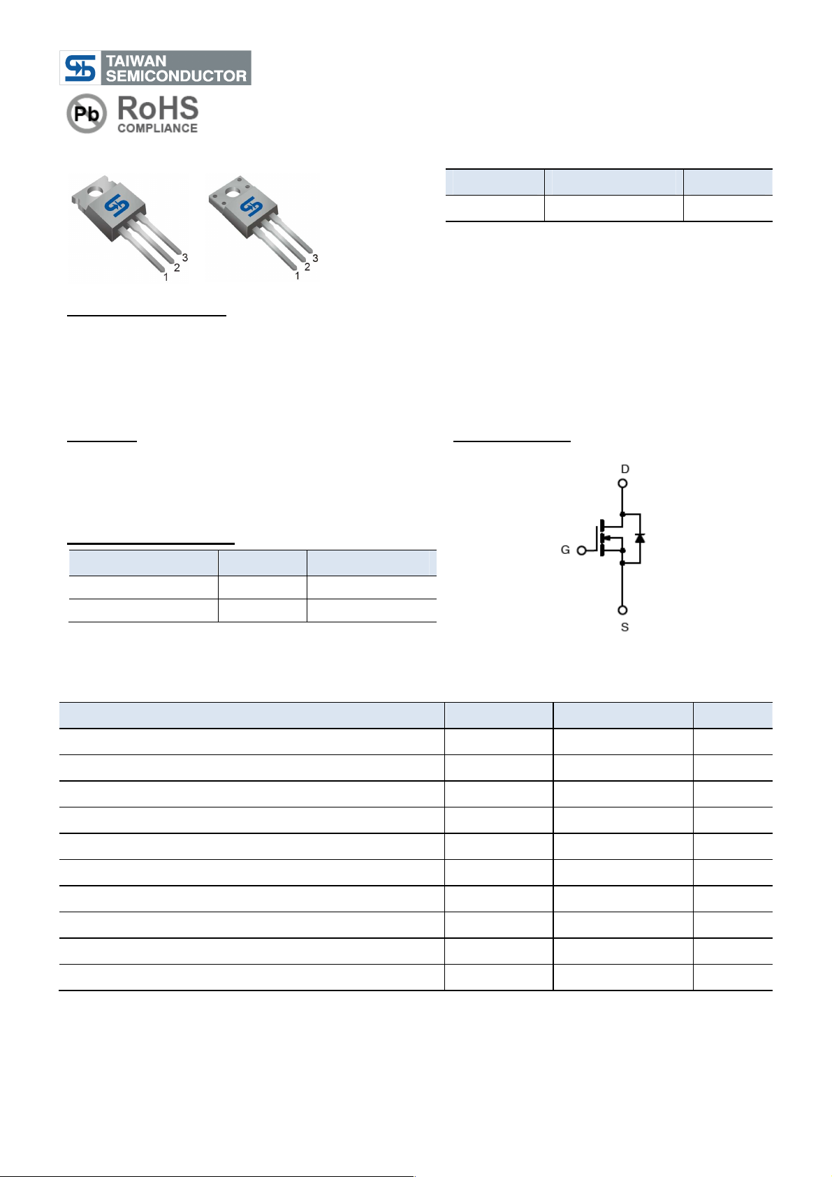
TO-220
ITO-220
PRODUCT SUMMARY
Pin Definition:
TSM20N50
500V N-Channel Power MOSFET
1. Gate
2. Drain
3. Source
General Description
The TSM20N50 N-Channel enhancement mode Power MOSFET is produced by planar stripe DMOS
technology. This advanced technology has been especially tailored to minimize on-state resistance, provide
superior switching performance, and withstand high energy pulse in the avalanche and commutation mode.
These devices are well suited for high efficiency switch mode power supply, electronic lamp ballast based on half
bridge.
VDS (V) R
500 0.3 @ V
(Ω) ID (A)
DS(on)
=10V 18
GS
Features
● Low R
● Low gate charge typical @ 54nC (Typ.)
● Improve dv/dt capability
DS(ON)
0.3Ω (Max.)
Block Diagram
Ordering Information
Part No. Package Packing
TSM20N50CZ C0 TO-220 50pcs / Tube
TSM20N50CI C0 ITO-220 50pcs / Tube
N-Channel MOSFET
Absolute Maximum Rating
(Ta = 25oC unless otherwise noted)
Parameter Symbol Limit Unit
Drain-Source Voltage VDS 500 V
Gate-Source Voltage VGS ±30 V
Continuous Drain Current(TC=25 )℃ ID 18 A
Pulsed Drain Current * IDM 72 A
Peak Diode Recovery dv/dt (Note 3) dv/dt 4.5 V/ns
Single Pulse Avalanche Energy (Note 2) EAS 954 mJ
Avalanche Current (Repetitive) (Note 1) IAR 18 A
Repetitive Avalanche Energy (Note 1) EAR 29 mJ
Operating Junction Temperature TJ 150 ºC
Storage Temperature Range T
* Limited by maximum junction temperature
1/10
-55 to +150
STG
o
C
Version: A12
Page 2
c
TSM20N50
500V N-Channel Power MOSFET
Thermal Performance
Parameter Symbol TO-220 ITO-220 Unit
Thermal Resistance - Junction to Case RӨJC 0.43 2.6
o
C/W
Thermal Resistance - Junction to Ambient RӨJA 62.5
Notes: Surface mounted on FR4 board t ≤ 10sec
Electrical Specifications
(Tc = 25oC unless otherwise noted)
Parameter Conditions Symbol Min Typ Max Unit
Static
Drain-Source Breakdown Voltage V
Drain-Source On-State Resistance V
Gate Threshold Voltage V
Zero Gate Voltage Drain Current V
Gate Body Leakage VGS = ±30V, VDS = 0V I
Forward Transconductance V
Diode Forward Voltage IS = 18A, VGS = 0V VSD -- -- 1.5 V
Dynamic b
Total Gate Charge
Gate-Source Charge Qgs -- 15 -Gate-Drain Charge Qgd -- 12.5 -Input Capacitance
Output Capacitance C
Reverse Transfer Capacitance C
Switching
Turn-On Delay Time
Turn-On Rise Time tr -- 72 -Turn-Off Delay Time t
Turn-Off Fall Time tf -- 68 -Reverse Recovery Time
Reverse Recovery Charge Qfr -- 6 -- uC
Notes:
1. Repetitive Rating: Pulse Width Limited by Maximum Junction Temperature
2. VDD = 50V, IAS=18A, L=5.3mH, RG=25Ω, Starting TJ=25℃
3. I
≤18A, di/dt ≤ 200A/uS, VDD ≤ BVDS, Starting TJ=25℃
SD
4. Pulse test: pulse width ≤300uS, duty cycle ≤2%
5. b For design reference only, not subject to production testing.
6. c Switching time is essentially independent of operating temperature.
= 0V, ID = 250uA BV
GS
= 10V, ID = 9.0A R
GS
= VGS, ID = 250uA V
DS
= 500V, VGS = 0V I
DS
= 30V, ID = 9.0A gfs -- 11 -- S
DS
500 -- -- V
DSS
-- 0.25 0.3 Ω
DS(ON)
2.0 -- 4.0 V
GS(TH)
-- -- 1 uA
DSS
-- -- ±100
GSS
Qg -- 54 --
V
= 400V, ID = 18A,
DS
V
= 10V
GS
C
V
= 25V, VGS = 0V,
DS
f = 1.0MHz
V
= 250V, ID = 18A,
DD
RG = 25Ω
V
= 0V, IS = 18A,
GS
-- 3094
iss
-- 296 --
oss
-- 9.2 --
rss
t
-- 78 --
d(on)
-- 184 --
d(off)
tfr -- 426 -- nS
--
dIF/dt = 100A/us
nA
nC
pF
nS
2/10
Version: A12
Page 3
500V N-Channel Power MOSFET
TSM20N50
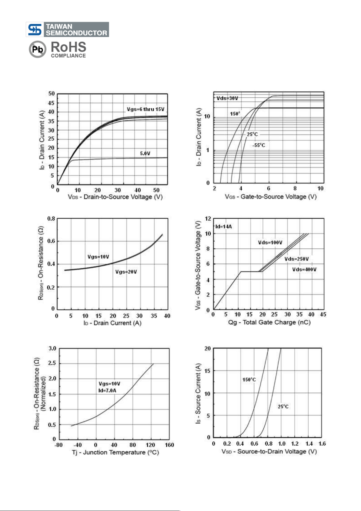
Electrical Characteristics Curve
Output Characteristics
On-Resistance vs. Drain Current
(Tc = 25oC, unless otherwise noted)
Transfer Characteristics
Gate Charge
On-Resistance vs. Junction Temperature
Source-Drain Diode Forward Voltage
3/10
Version: A12
Page 4

500V N-Channel Power MOSFET
Electrical Characteristics Curve
(Ta = 25oC, unless otherwise noted)
TSM20N50
Drain Current vs. Case Temperature
Maximum Safe Operating Area
BV
vs. Junction Temperature
DSS
Capacitance vs. Drain-Source Voltage
Maximum Safe Operating Area (ITO-220)
4/10
Version: A12
Page 5

500V N-Channel Power MOSFET
Electrical Characteristics Curve
Normalized Thermal Transient Impedance, Junction-to-Ambient
Normalized Thermal Transient Impedance, Junction-to-Ambient(ITO-220)
(Ta = 25oC, unless otherwise noted)
TSM20N50
5/10
Version: A12
Page 6
500V N-Channel Power MOSFET
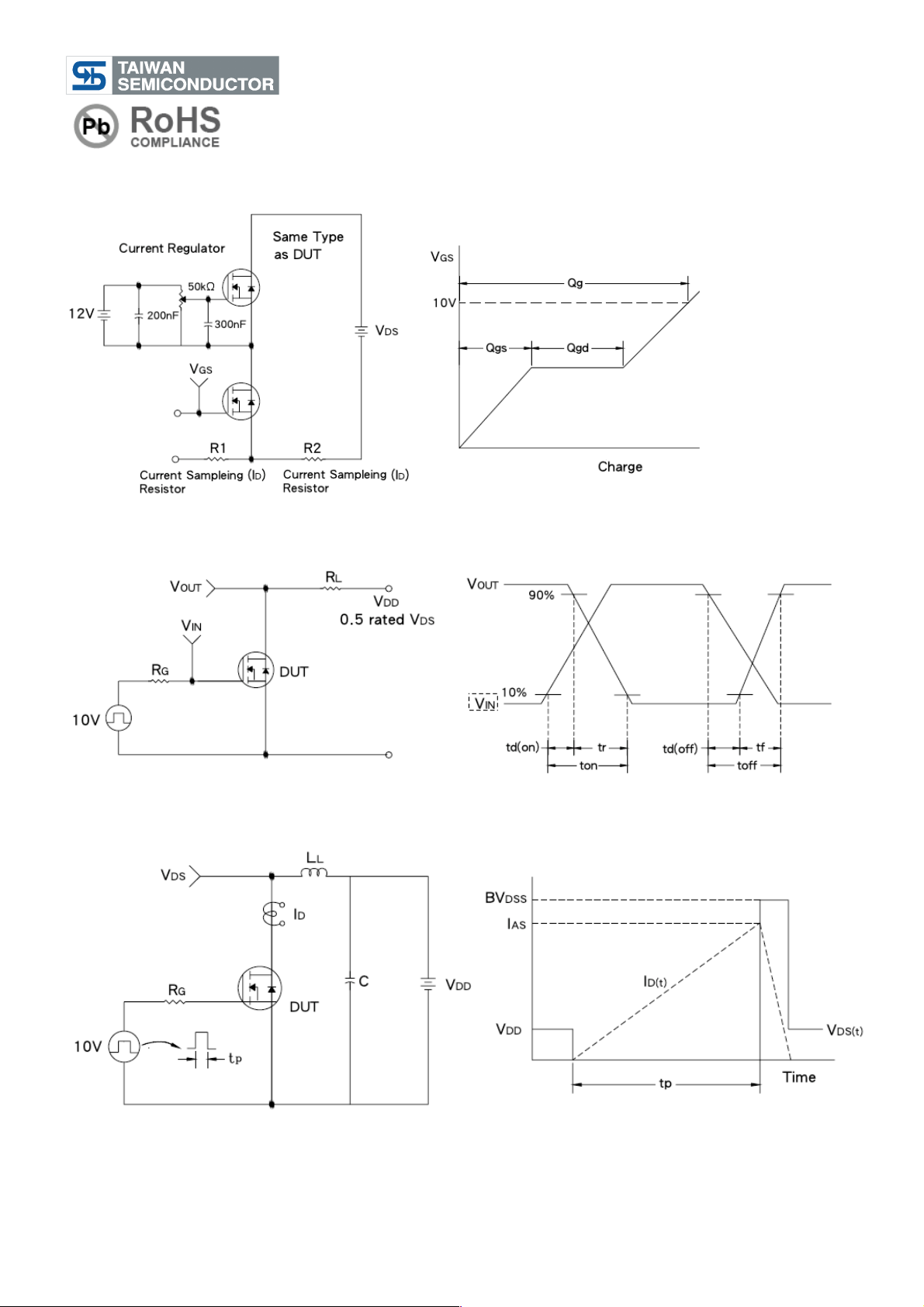
Gate Charge Test Circuit & Waveform
Resistive Switching Test Circuit & Waveform
TSM20N50
EAS Test Circuit & Waveform
6/10
Version: A12
Page 7

500V N-Channel Power MOSFET
Diode Reverse Recovery Time Test Circuit & Waveform
TSM20N50
7/10
Version: A12
Page 8

500V N-Channel Power MOSFET
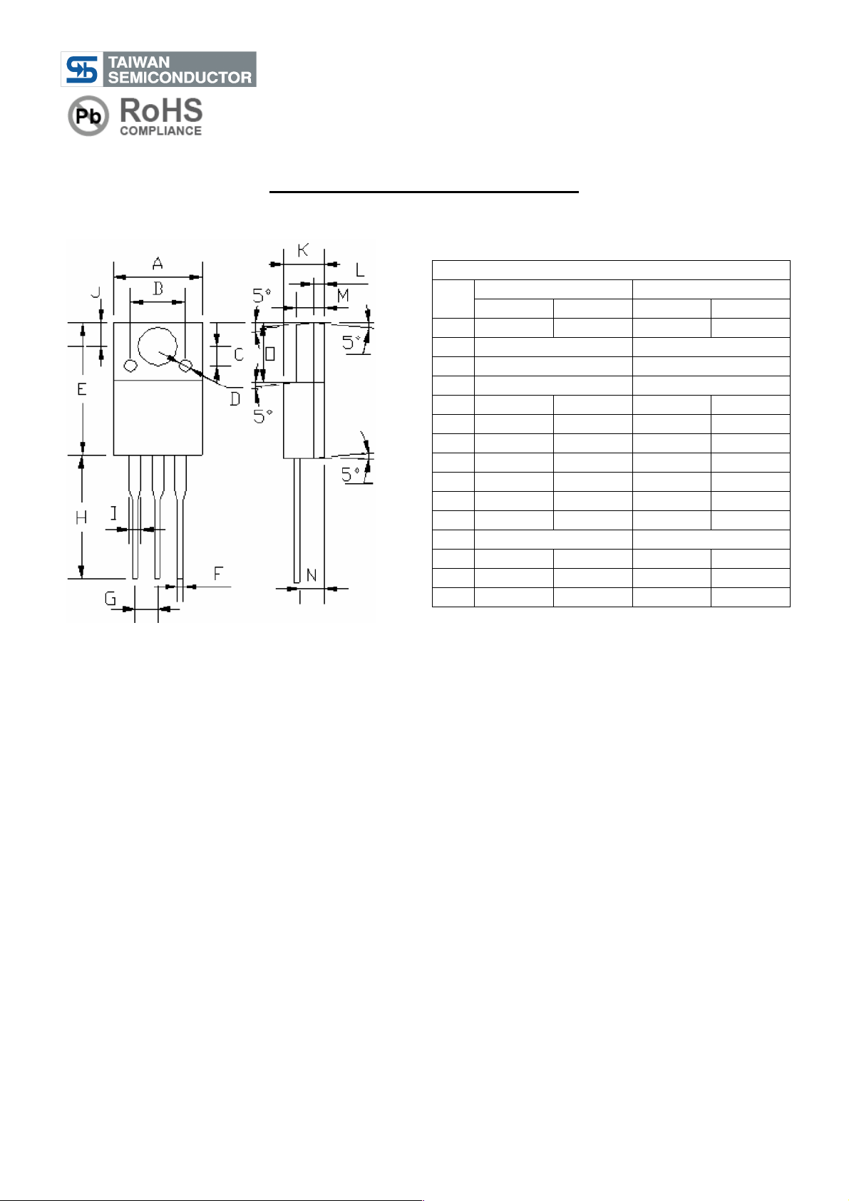
TO-220 Mechanical Drawing
TO-220 DIMENSION
DIM
A 10.00 10.50 0.394 0.413
B 3.74 3.91 0.147 0.154
C 2.44 2.94 0.096 0.116
D -- 6.35 -- 0.250
E 0.38 1.10 0.015 0.043
F 2.34 2.71 0.092 0.107
G 4.69 5.43 0.185 0.214
H 12.70 14.73 0.500 0.580
I 8.38 9.38 0.330 0.369
J 14.22 16.51 0.560 0.650
K 3.55 4.82 0.140 0.190
L 1.16 1.40 0.046 0.055
M 27.70 29.62 1.091 1.166
N 2.03 2.92 0.080 0.115
O 0.25 0.61 0.010 0.024
P 5.84 6.85 0.230 0.270
MILLIMETERS INCHES
MIN MAX MIN MAX
TSM20N50
8/10
Version: A12
Page 9
500V N-Channel Power MOSFET
ITO-220 Mechanical Drawing
ITO-220 DIMENSION
DIM
A 10.04 10.07 0.395 0.396
B 6.20 (typ.) 0.244 (typ.)
C 2.20 (typ.) 0.087 (typ.)
D ∮1.40 (typ.) ∮0.055 (typ.)
E 15.0 15.20 0.591 0.598
F 0.52 0.54 0.020 0.021
G 2.35 2.73 0.093 0.107
H 13.50 13.55 0.531 0.533
I 1.11 1.49 0.044 0.058
J 2.60 2.80 0.102 0.110
K 4.49 4.50 0.176 0.177
L 1.15 (typ.) 0.045 (typ.)
M 3.03 3.05 0.119 0.120
N 2.60 2.80 0.102 0.110
O 6.55 6.65 0.258 0.262
MILLIMETERS INCHES
MIN MAX MIN MAX
TSM20N50
9/10
Version: A12
Page 10

TSM20N50
500V N-Channel Power MOSFET
Notice
Specifications of the products displayed herein are subject to change without notice. TSC or anyone on its behalf,
assumes no responsibility or liability for any errors or inaccuracies.
Information contained herein is intended to provide a product description only. No license, express or implied, to
any intellectual property rights is granted by this document. Except as provided in TSC’s terms and conditions of
sale for such products, TSC assumes no liability whatsoever, and disclaims any express or implied warranty,
relating to sale and/or use of TSC products including liability or warranties relating to fitness for a particular purpose,
merchantability, or infringement of any patent, copyright, or other intellectual property right.
The products shown herein are not designed for use in medical, life-saving, or life-sustaining applications.
Customers using or selling these products for use in such applications do so at their own risk and agree to fully
indemnify TSC for any damages resulting from such improper use or sale.
10/10
A12
Version:
 Loading...