

Page 1
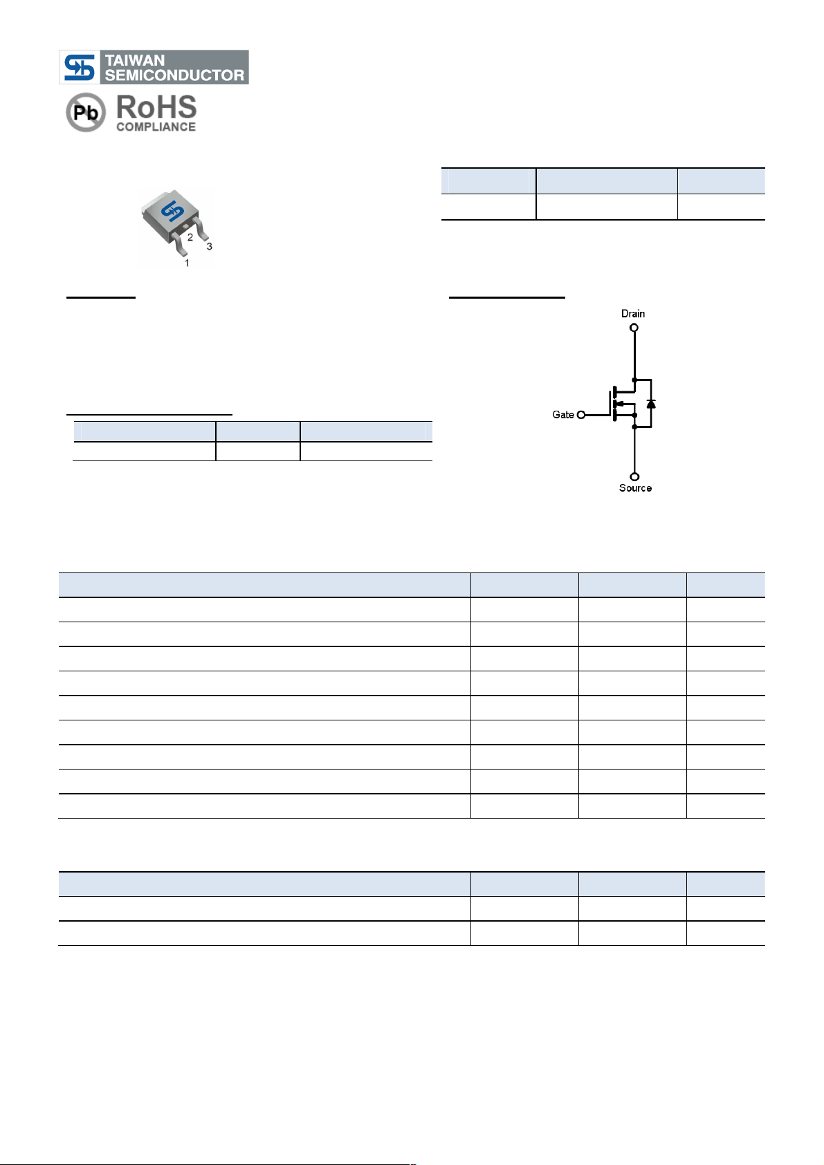
TO-252
PRODUCT SUMMARY
Pin
Definition
:
200V N-Channel Power MOSFET
(DPAK)
1. Gate
2. Drain
3. Source
VDS (V) R
200 92 @ V
DS(on)
TSM19N20
(mΩ) ID (A)
=10V 18
GS
Features
● Advanced Trench Technology
● Low R
● Low gate charge typical @ 55nC (Typ.)
● Low Crss typical @ 73pF (Typ.)
92mΩ (Max.)
DS(ON)
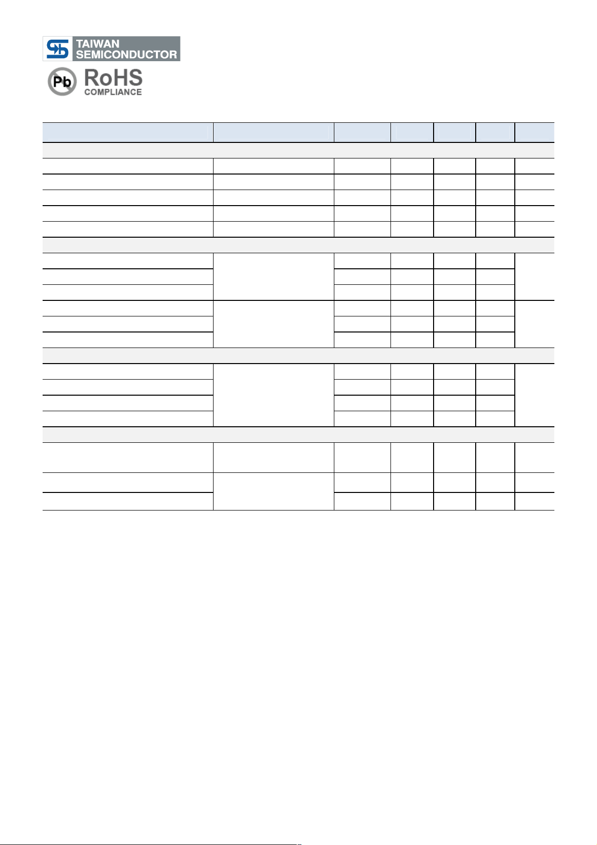
Block Diagram
Ordering Information
Part No. Package
TSM19N20CP ROG
Note: “G” denote for Halogen Free Product
Absolute Maximum Rating
TO-252 2.5Kpcs / 13” Reel
(Ta = 25oC unless otherwise noted)
Parameter Symbol Limit Unit
Drain-Source Voltage VDS 200 V
Gate-Source Voltage VGS ±20 V
Continuous Drain Current @ TC=25°C ID 18 A
Drain Current Pulsed (Note 1) IDM 72 A
Packing
N-Channel MOSFET
Avalanche Current IAS 8 A
Avalanche Energy, L=10mH EAS 320 mJ
Maximum Power Dissipation @ TC=25°C PD 48 W
Storage Temperature Range T
Operating Junction Temperature Range TJ -55 to +150 °C
* Limited by maximum junction temperature
Thermal Performance
-55 to +150 °C
STG
Parameter Symbol Limit Unit
Thermal Resistance - Junction to Case RӨJC 2.6
Thermal Resistance - Junction to Ambient RӨJA 50
Notes: Surface mounted on FR4 board t ≤ 10sec
o
C/W
o
C/W
1/4
Version: A12
Page 2
200V N-Channel Power MOSFET
Electrical Specifications
(Ta = 25oC unless otherwise noted)
TSM19N20
Parameter Conditions Symbol
Min Typ Max Unit
Static
Drain-Source Breakdown Voltage V
Drain-Source On-State Resistance V
Gate Threshold Voltage V
Zero Gate Voltage Drain Current V
Gate Body Leakage VGS = ±30V, VDS = 0V I
= 0V, ID = 250uA BV
GS
= 10V, ID = 10A R
GS
= VGS, ID = 250uA V
DS
= 160V, VGS = 0V I
DS
200 -- -- V
DSS
-- 80 92 mΩ
DS(ON)
2 -- 4 V
GS(TH)
-- -- 1 uA
DSS
-- -- ±100
GSS
Dynamic
Total Gate Charge
V
= 100V, ID = 10A,
Gate-Source Charge Qgs -- 18 -Gate-Drain Charge Qgd -- 17 --
V
DS
= 10V
GS
Input Capacitance
V
= 30V, VGS = 0V,
Output Capacitance C
DS
f = 1.0MHz
Reverse Transfer Capacitance C
Qg -- 55 --
C
-- 2300 --
iss
-- 145 --
oss
-- 73 --
rss
Switching
Turn-On Delay Time
Turn-On Rise Time tr -- 12 -Turn-Off Delay Time t
V
= 10V, V
GS
RG = 3Ω
= 100V,
DS
t
-- 17 --
d(on)
-- 28 --
d(off)
Turn-Off Fall Time tf -- 10 --
Drain-Source Diode Characteristics and Maximum Rating
Drain-Source Diode Forward
Voltage
VGS=0V, IS=10A VSD -- -- 1.3 V
nA
nC
pF
nS
Reverse Recovery Time
Reverse Recovery Charge Qfr -- 276 -- nC
IS = 10A, TJ=25 oC
dI/dt = 100A/us
tfr -- 82 -- nS
Notes:
1. Pulse Test: Pulse Width ≤ 300µs, Duty Cycle ≤ 2%.
2. RθJA is the sum of the junction-to-case and case-to-ambient thermal resistance where the case thermal
reference is defined as the solder mounting surface of the drain pins. RθJC is guaranteed by design while RθCA
is determined by the user's board design. RθJA shown below for single device operation on FR-4 in still air
2/4
Version: A12
Page 3

200V N-Channel Power MOSFET
TO-252 Mechanical Drawing
TSM19N20
Unit: Millimeters
3/4
Version: A12
Page 4

TSM19N20
200V N-Channel Power MOSFET
Notice
Specifications of the products displayed herein are subject to change without notice. TSC or anyone on its behalf,
assumes no responsibility or liability for any errors or inaccuracies.
Information contained herein is intended to provide a product description only. No license, express or implied, to
any intellectual property rights is granted by this document. Except as provided in TSC’s terms and conditions of
sale for such products, TSC assumes no liability whatsoever, and disclaims any express or implied warranty,
relating to sale and/or use of TSC products including liability or warranties relating to fitness for a particular purpose,
merchantability, or infringement of any patent, copyright, or other intellectual property right.
The products shown herein are not designed for use in medical, life-saving, or life-sustaining applications.
Customers using or selling these products for use in such applications do so at their own risk and agree to fully
indemnify TSC for any damages resulting from such improper use or sale.
4/4
Version: A12
 Loading...