

Page 1

Features
• Programmable DMUX Ratio:
– 1:4: Data Rate Max = 1 Gsps
– PD (8b/10b) < 4.3/4.7 W (ECL 50Ω output)
– 1:8: Data Rate Max = 2 Gsps
– PD (8b/10b) < 6/6.9 W (ECL 50Ω output)
– 1:16 with 1 TS8388B or 1 TS83102G0B and 2 DMUX
• Parallel Output Mode
• 8-/10-bit
• ECL Differential Input Data
• DataReady or DataReady/2 Input Clock
• Input Clock Sampling Delay Adjust
• Single-ended Output Data:
– Adjustable Common Mode and Swing
– Logic Threshold Reference Output
– (ECL, PECL, TTL)
• Asynchronous Reset
• Synchronous Reset
• ADC + DMUX Multi-channel Applications:
– Stand-alone Delay Adjust Cell for ADCs Sampling Instant Alignment
• Differential Data Ready Output
• Built-in Self Test (BIST)
• Dual Power Supply V
• Radiation Tolerance Oriented Design (More than 100 Krad (Si) Expected)
• TBGA 240 (Cavity Down) Package
= -5V, VCC = +5V
EE
DMUX 8-/10-bit
2 GHz 1:4/8
TS81102G0
Description
The TS81102G0 is a monolithic 10-bit high-speed (up to 2 GHz) demultiplexor,
designed to run with all kinds of ADCs and more specifically with Atmel’s high-speed
ADC 8-bit 1 Gsps TS8388B and ADC 10-bit 2 Gsps TS83102G0B.
The TS81102G0 uses an inn ovative architecture, including a sampling delay adjust
and tunable output levels. It allows users to process the high-speed output data
stream down to processor speed and uses the very high-speed bipolar technology (25
GHz NPN cut-off frequency).
Rev. 2105C–BDC–11/03
1
Page 2
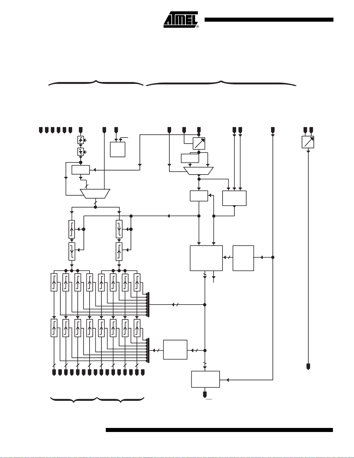
Block Diagram
Figure 1. Block Diagram
Data Path Clock Path
SwiAdj
VplusDOut
VCC
even
master
latch
even
slave
latch
GND
VEE
DIODE
BIST
8/10
BIST
8/10
FS/8
mux
I[0..7/9]
odd
master
latch
odd
slave
latch
NbBit
NAP
RatioSel
DEMUXDelAdjCtrl
ClkInType
B 2
Phase
control
ClkPar
shift register)
Port Selection Clock
8
ClkIn
delay
mux
Counter
(8 stage
8
FS/8
AsyncReset
SyncReset
(to be confirmed)
RstGen
Reset
8
Counter
Status
RatioSel
ADCDelAdjCtrl
ADCDelAdjIn
delay
Latch Sel Even/Odd [1..8/10]
Data
8
Output
Clock
8/10
A[0..7/9]
C[0..7/9]
E[0..7/9]
G[0..7/9]
B[0..7/9]
D[0..7/9]
F[0..7/9]
RefA
RefC
RefE
RefG
RefB
RefD
Even Ports Odd Ports
2
TS81102G0
H[0..7/9]
RefF
RefH
1
3
DataReady
generation
DR/DR
ADCDelAdjOut
2105C–BDC–11/03
Page 3
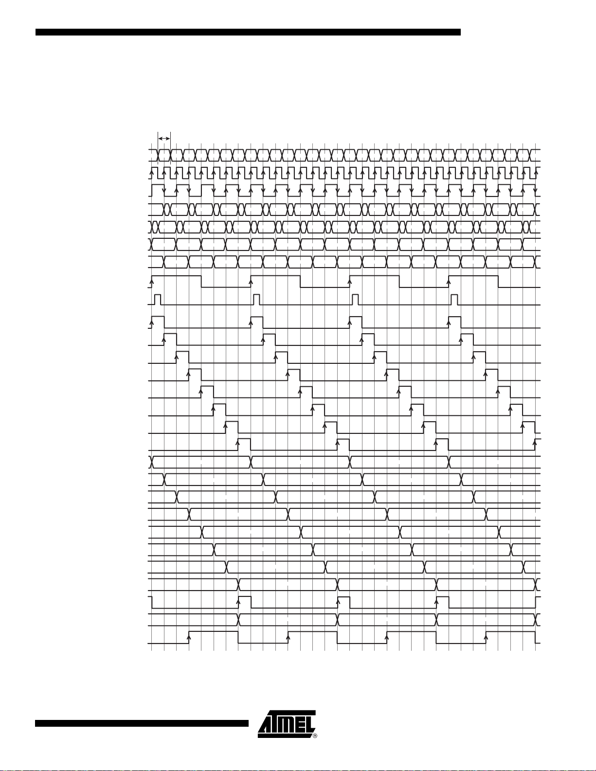
TS81102G0
Internal Timing
This diagram corresponds to an established opera tion of the DMUX with Synchronous Reset.
Diagram
Figure 2. Internal Timing Diagram
500 ps min
N N+2 N+3 N+4 N+5 N+6 N+7 N+8 N+9 N+10 N+11 N+12 N+13 N+14 N+15 N+16 N+17 N+18 N+19 N+20 N+21 N+22 N+23 N+24
Data In
DR In = Fs
DR/2 In = Fs/2 = ClkPar
Master Even Latch
Master Odd Latch
Slave Even Latch
Slave Odd Latch
Synchronous reset = Fs/8
Internal reset pulse
Port Select A
Port Select B
Port Select C
N+1
N+1 N+31
N
N+1
N+25 N+26 N+27 N+28 N+29 N+30 N+31
N+24 N+26 N+28 N+30N+14 N+16 N+18 N+20 N+22N+6 N+8 N+10 N+12N N+2 N+4
N+3 N+5 N+7 N+9 N+11 N+13 N+15 N+17 N+19 N+21 N+23 N+25 N+27 N+29
N+2
N+4
N+6
N+8
N+10
N+12
N+14
N+16
N+18
N+20
N+22
N+24
N+26
N+3
N+5
N+7
N+9
N+11
N+13
N+15
N+17
N+19
N+21
N+23
N+25
N+27
N+28
N+30
N+29
Port Select D
Port Select E
Port Select F
Port Select G
Port Select H
Latch Select A
Latch Select B
Latch Select C
Latch Select D
Latch Select E
Latch Select F
Latch Select G
Latch Select H
A to H Port Out
A to H LatchOut
DROut
N N+8 N+16 N+24
N+1 N+9 N+17 N+25
N+2 N+10 N+18 N+26
N+3 N+11 N+19 N+27
N+4 N+12 N+20
N+5 N+13 N+21
N+6 N+14 N+22
N+7 N+15 N+23
N to N+7 N+8 to N+15 N+16 to N+23
2105C–BDC–11/03
3
Page 4

Functional
Description
The TS81102G0 is a demultiplexer based on an advanced high-speed bipolar technology featuring a cutoff frequency of 25 GHz. Its role is to reduce the data rate so that the data can be
processed at the DMUX output.
The TS81102G0 provides 2 programmable ratios: 1:4 and 1:8. The maximum data rate is 1
Gsps for the 1:4 ratio and 2 Gsps for the 1:8 ratio.
The TS81102G0 is able to process 8 or 10-bit data flows.
The input clock can be an ECL differential signal or single-ended DC cou pled signal. Mo reover
it can be a DataReady or DataReady/2 clock.
The input digital data must be an ECL differential signal.
The output signals (Data Ready, digital data and reference voltage) are adjustable with
VplusD independent power supply. Typical output modes are ECL, PECL or TTL.
The Data Ready output is a differential signal. The digital output data and reference voltages
are single-ended signals.
The TS81102G0 is started by an Asynchronous Reset. A Synchronous Reset enables the
user to re-synchronize the output port selection and to minimize loss of data that could occur
within the DMUX.
A delay adjust cell is available to ensure a good phase between the DMUX’ input clock and
input data.
Another delay adjust cell is available to contro l the ADCss sampling instant alignment, in case
of the ADCs interleaving.
A 10-bit generator is implemented in the TS81102G0, the Built-In Self Test (BIST). This test
sequence is very useful for testing the DMUX at first use.
A fine tuning of the output swing is also available.
The TS81102G0 can be used with the following Atmel ADCs:
• TS8388B(F/FS/GL), 8-bit 1 Gsps ADC
• TS83102G0B, 10-bit 2 Gsps ADC
4
TS81102G0
2105C–BDC–11/03
Page 5
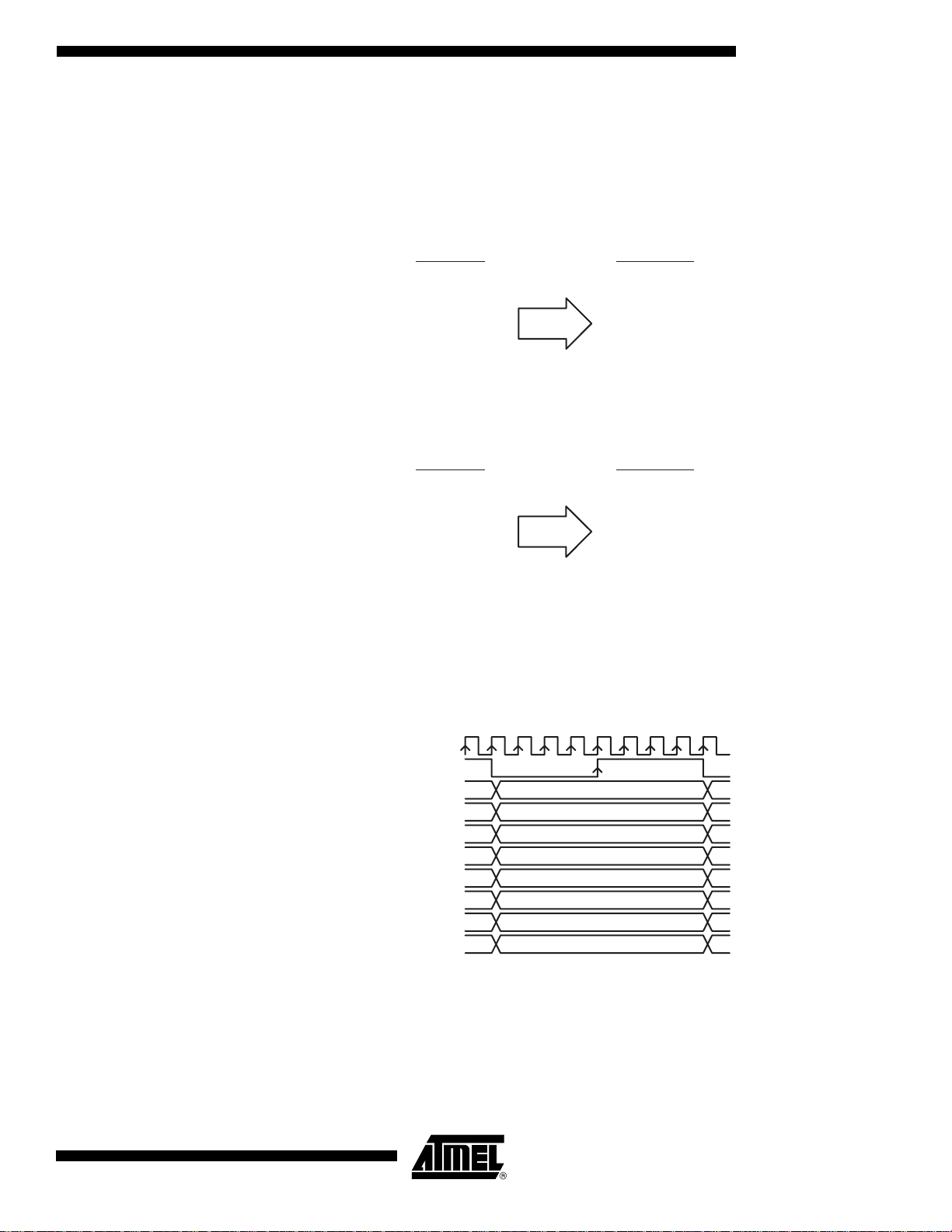
Main Function
Description
TS81102G0
Programmable
DMUX Ratio
The conversion ratio is programmable: 1:4 or 1:8.
Figure 3. Programmable DMUX Ratio
Input Words:
1,2,3,4,5,6,7,8,...
1:4
Input Words:
1,2,3,4,5,6,7,8,...
1:8
Output Words:
PortA
PortB
PortC
PortD
PortE
PortF
PortG
PortH
Output Words:
PortA
PortB
PortC
PortD
PortE
PortF
PortG
PortH
1
2
3
4
not used
not used
not used
not used
1
2
3
4
5
6
7
8
5
6
7
8
9
10
11
12
13
14
15
16
...
...
Parallel Output
Mode
Figure 4. Parallel Mode
ClkIn
DR
PortA
PortB
PortC
PortD
PortE
PortF
PortG
PortH
Input Clock Sampling Delay Adjust (DEMUXDELADJCTRL)
The input clock phase can be adjusted with an adjustable delay (from 250 to 750 ps). This is to
ensure a proper phase between the clock and input data of the DMUX.
2105C–BDC–11/03
N
N+1
N+2
N+3
N+4
N+5
N+6
N+7
5
Page 6
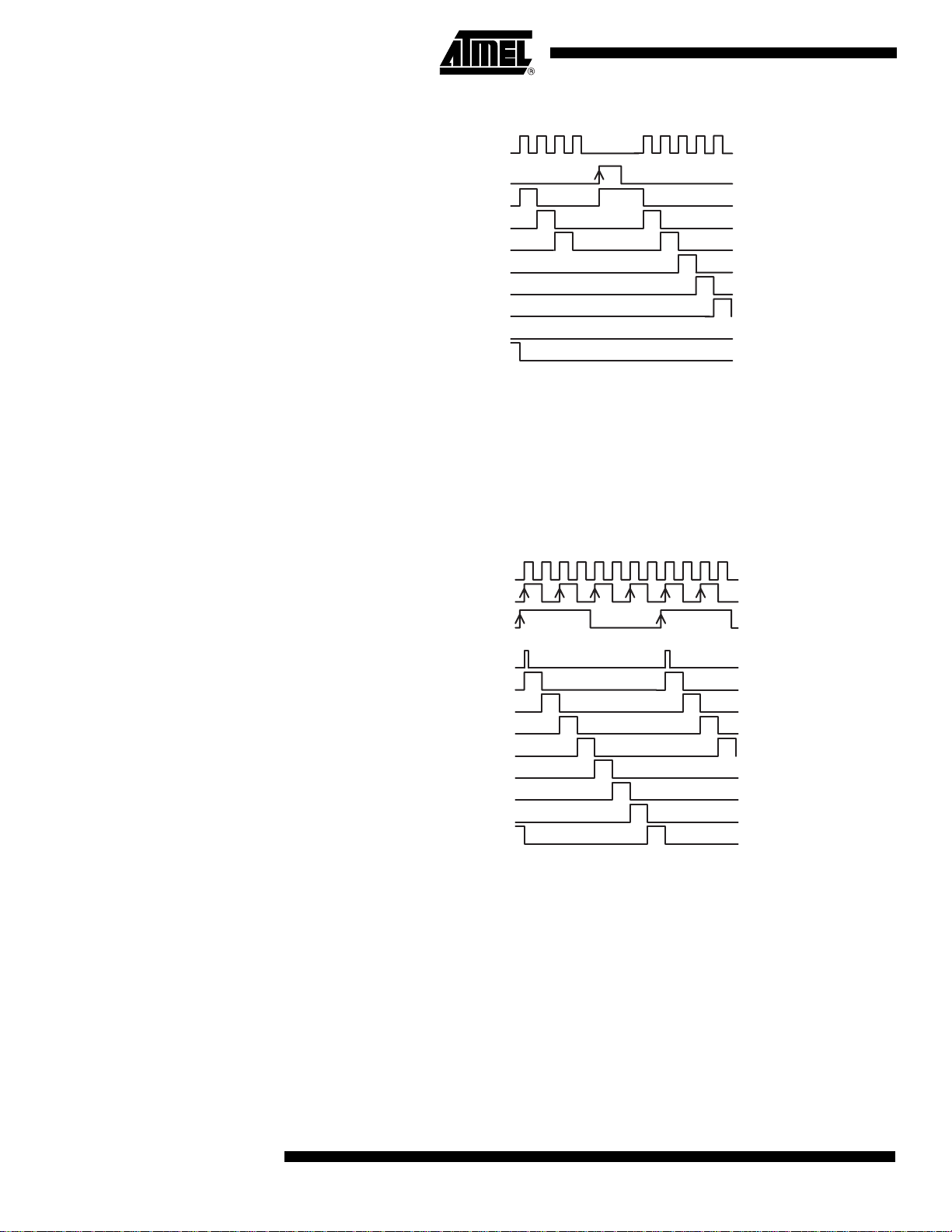
Asynchronous
Reset
(ASYNCRESET)
Figure 5. Asynchronous Reset
CLKIN
AsyncReset
Port A selected
Port B selected
Port C selected
Port D selected
Port E selected
Port F selected
Port G selected
Port H selected
The Asynchronous Reset is a master reset of the port selection, which works on TTL levels. It
is active on the high level. During an asynchronous reset, the clock must be in a known state.
It is used to start the DMUX.
When it is active, it paralyzes the outputs (the out put clock and output d ata remain at the same
level as before the asynchronous reset). When it comes back to its low leve l, the DMUX star ts:
the outputs are active and the first processed data is on port A.
Synchronous
Reset
(SYNCRESET)
Figure 6. Synchronous Reset
FS
DR/2
SyncReset = FS/8
Internal reset
pulse
Port A selected
Port B selected
Port C selected
Port D selected
Port E selected
Port F selected
Port G selected
Port H selected
The DMUX can be synchronously reset to a programmable state dependin g on the conversion
ratio. The clock must not be stopped during reset. The synchronizat ion signal is a clock
(SyncRest) whose frequency is FS/8*n where n is an integer (n = 1,2,3,…) in 1:8 mode and
FS/4*n in 1:4 mode. The front edge of this clock is synchronized with Clkln inside the DMUX,
and generates a 200 ps reset pulse. This reset pulse occurs during a f ixed level of Clkln.
If the DMUX was synchronized with Syncreset previous to a possible loss of synchronization,
then the output data is immediately corre ct, no modification can b e seen at the output o f the
DMUX, and no data is lost (“Internal Timing Diagram” on page 3).
If the DMUX was not synchronized with SyncReset previous to a possible lo ss o f syn chronization, then the output data and data r eady of the DM UX are chang ed. The outp ut data is corr ect
after a number of input clocks corresponding to the pipe line delay (“Timing Diagr ams with Synchronous Reset” on page 19).
6
TS81102G0
2105C–BDC–11/03
Page 7
TS81102G0
Counter
Programmable
State
When the counter is reset, its initial states depends on the conversion ratio:
• 1:8: counting on 8 bits,
• 1:4: counting on 4 bits.
Pipeline Delay The maximum pipeline delay depends on the conversion ratio:
• 1:8: pipeline delay = 7
• 1:4: pipeline delay = 3
8-/10-bit, with NAP
Mode for the 2
The DMUX is a 10-bit parallel device. The last two bits (bits 8 and 9) may not be used, a nd the
corresponding functions are set to nap mode to reduce power consumption.
Unused Bit
ECL Differential
Input Data
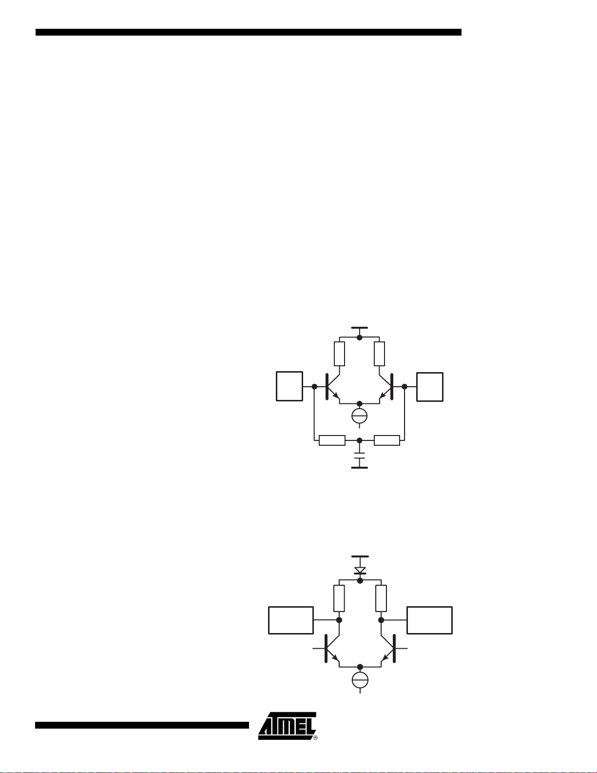
Input data are ECL compatible (Voh = -0.8V, Vol = -1.8V).
The minimum swing required is 100 mV differential.
All inputs have a 100Ω differential termination resistor. The middle point of these resistor s is
connected to ground through a 10 pF capacitor.
Figure 7. ECL Differential Input Data
Gnd
50Ω Differential
Output Data
ClkIn ClkInb
50Ω 50Ω
10 pF
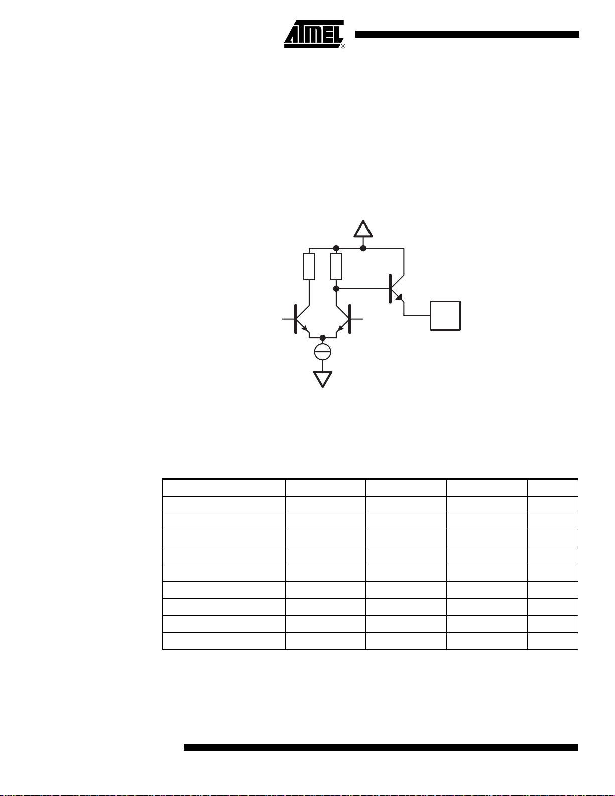
The output clock for the ADC is generate d th ro ug h a 50Ω loaded long tailed. The 50Ω resistor
is connected to the ground pad via a diode. The levels are (on the 100Ω differential termination resistor): Vol = -1.4V, Voh = -1.0V.
Figure 8. 50Ω Differential Output Data
Gnd
50Ω
ADCDelAdjOut
50Ω
ADCDelAdjOutb
2105C–BDC–11/03
7
Page 8
Single-ended
Output Data
To reduce the pin number and power consumption of the DMUX, the eight output ports are
single-ended.
To reach the high frequency output (up to 250 MHz) with a reasonable power consumption,
the swing must be limited to a maximum of ±500 mV. The common mode is adjustab le from
-1.3V to +2V, with Vplus DOut pins. To ensure better noise immunity, a reference level (common mode) is available (one level by output port).
The output buffers are of ECL type (open emitters – not resistive adapted impedances). They
are designed for a 15 mA average output current, and may be used with a 50Ω termin ation
impedance.
Figure 9. Single-ended Output Data
VPlusDOut
PadOut
Vee
Following are three application examples for these buffers: ECL/PECL/TTL. Please note that it
is possible to have any other odd output format as far as current (36 mA max) and voltage
(Vplus Dout – V
≤ 8.3V) limits are not overrid den. The maximum frequency in TTL output
EE
mode depends on the load to be driven.
Table 1. Examples of Application of Buffers
Parameter ECL PECL TTL Unit
VplusDout 0 3.3 3.3 V
Vtt -2 1.3 0 V
Swing ±0.5 ±0.5 ±1 V
Reference -1.3 2 1.5 V
Voh -0.8 2.5 2.5 V
Vol -1.8 1.5 0.5 V
Load 50 50 ≥75 Ω
Average Output Current 14 14 15 mA
Output Data rate max. 250 250 250 Msps
This corresponds to the “Adjustable Logic Single” in the pinout description.
The “Adjustable Single” buffers for reference voltage are the same buffers, but the information
available at the output of these buffers is more like analog than logic.
Note: The Max Output Data Rate is given for a typical 50Ω/2 pF load.
8
TS81102G0
2105C–BDC–11/03
Page 9
TS81102G0
Differential Data
Ready Output
Built-in Self Test
(BIST)
Specifications
Absolute
Maximum Ratings
The front edge of the DataReady output occurs when data is available on the correspo nding
port. The frequency of this clock depends on the conversion ratio (1: 8 or 1:4), with a dut y cycle
of 50%.
The definition is the same as for single-ended output data, but the buffers are differential.
This corresponds to the “Adjustable Logic Differential” in the pinout description.
A pseudo-random 10-bit generator is impleme nted in t he DMUX. It generat es a 10-bit signal in
the output of the DMUX, with a period of 512 input clocks. The probability of occurrence of
codes is uniformly spread over the 1024 possible codes: 0 or 1/1024.
Note that the 256 codes of bits 1 to 8 occur at least once. They start with a BIST command, in
phase with the FS/8 clock on Port A. The logic output obt ained on the A to H ports depend s on
the conversion ratio. The driving clock of BIST is Clkln. The ClklnType must be set to ‘1’
(DataReady ADC clock) to have a different 10-bit code on each output.
The complete BIST sequence is available on request.
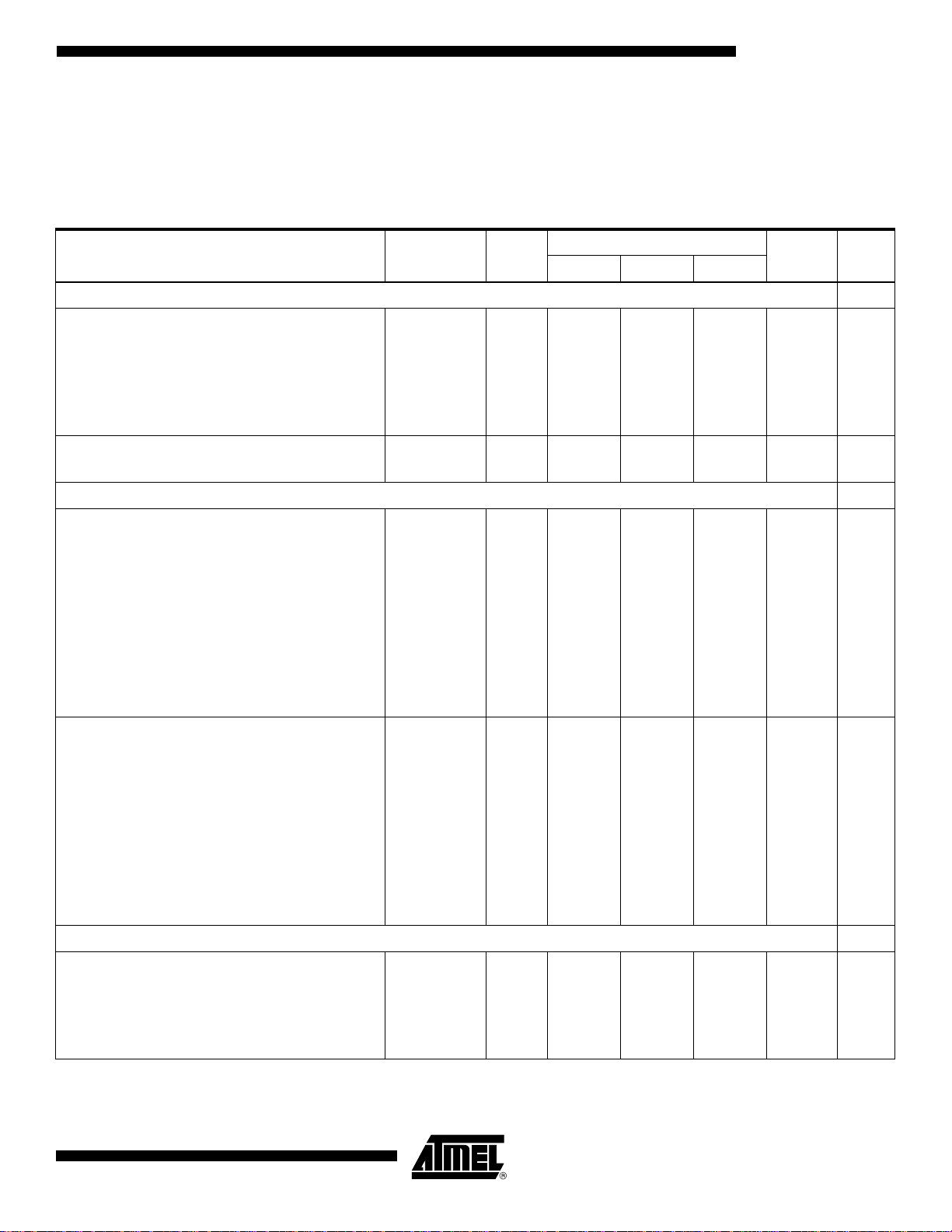
Table 2. Absolute Maximum Ratings
Parameter Symbol Comments Value Unit
Positive supply voltage V
Positive output buffer supply voltage V
Negative supply voltage V
Analog input voltages ADCDelAdjCtrl,
ECL 50Ω input voltage Clkln or Clklnb or
Maximum difference between ECL 50Ω
input voltages
CC
PLUSD
EE
ADCDelAdjCtrlb or
DMUXDelAdjCtrl,
DMUXDelAdjCtrlb or
SwiAdj
I[0…9] or I[0…9]b or
SyncReset or
SyncResetb or
ADCDelAdjln or
ADCDelAdjlnb
Clkln – Clklnb or
I[0…9] - I[0…9]b or
SyncReset –
Syncresetb or
ADCDelAdjln ADCDelAdjlnb
Voltage range for each
pad
Differential voltage
range
Voltage range for each
pad
Minimum differential
swing
Maximum differential
swing
GND to 6 V
GND to 4 V
GND to -6 V
-1 to +1
-1 to +1
-2.2 to +0.6 V
0.1
2
V
V
2105C–BDC–11/03
9
Page 10
Table 2. Absolute Maximum Ratings (Continued)
Parameter Symbol Comments Value Unit
Data output current A[0…9] to H[0…9] or
RefA to RefH or
DR or DRb
Maximum current 36 mA
TTL input voltage Clkln Type
GND to V
CC
V
RatioSel
NbBit
AsyncReset
BIST
Maximum input voltage on diode for
DIODE 700 mV
temperature measurement
Maximum input current on diode DIODE 8 mA
Maximum junction temperature T
Storage temperature T
j
stg
135 °C
-65 to 150 °C
Note: Absolute maximum ratings are limiting values, to be applied individually, while other parameters are within specified operating
conditions. Long exposure to maximum rating may affect device reliability. The use of a thermal heat sink is mandator y. See
“Thermal and Moisture Characteristics” on page 26.
Recommended
Operating
Conditions
Table 3. Recommended Operating Conditions
Parameter Symbol Comments
Positive supply voltage V
Positive output buffer supply
voltage
Positive output buffer supply
voltage
Positive output buffer supply
voltage
Negative supply voltage V
Operating temperature range T
10
TS81102G0
CC
V
PLUSD
V
PLUSD
V
PLUSD
EE
J
ECL output compatibility – 0 – V
PECL output compatibility – 3.3 – V
TTL output compatibility – 3.3 – V
Commercial grade: “C”
Industrial grade: “V”
Recommended Value
Min Typ Max Unit
4.45 5 5.25 V
-5.25-5-4.75V
0 < Tc; Tj < 90
°C
-40 < Tc; Tj < 110
2105C–BDC–11/03
Page 11
TS81102G0
Electrical
Operating
Tj (typical) = 70°C. Full Temperature Range: -40°C < Tc; Tj < 110°C.
(Guaranteed temperature range are depending on part number)
Characteristics
Table 4. Electrical Specifications
Parameter Symbol
Power Requirements
Positive supply voltage
V
V
PLUSD
V
PLUSD
V
PLUSD
V
I
I
PLUSD
I
I
PLUSD
I
I
PLUSD
I
I
PLUSD
I
I
I
PLUSD
I
I
PLUSD
I
I
PLUSD
I
I
PLUSD
I
Negative supply voltage
Supply Currents
ECL (50Ω) and PECL (50Ω)
V
(for every configuration)
CC
1:8, 8 bits
1:8, 10 bits
1:4, 8 bits
1:4, 10 bits
TTL (75Ω)
(for every configuration)
V
CC
1:8, 8 bits
1:8, 10 bits
1:4, 8 bits
1:4, 10 bits
Nominal power dissipation
V
PLUSDOUT
PECL
V
CC
ECL
TTL
V
EE
–
CC
EE
EE
EE
EE
CC
EE
EE
EE
EE
CC
EE
Test
Value
Level
4.75
–
1
-0.25
3.135
3.135
5
–
0
3.3
3.3
5.25
–
0.25
3.465
3.465
1 -5.25 -5 -4.75 V
–
540
–
640
1
–
270
–
320
–
–
760
–
900
1
–
380
–
450
–
31
1180
719
1140
790
590
592
720
634
31
1610
872
1770
980
810
670
880
729
–
1820
–
2240
–
910
–
1120
–
–
2440
–
3010
–
1220
–
1510
–
Unit NoteMin Typ Max
V
–
V
V
V
(1)
mA
mA
mA
mA
mA
mA
mA
mA
mA
mA
mA
mA
mA
mA
mA
mA
mA
mA
(1)
ECL (50Ω)
1:8, 8 bits
1:8, 10 bits
1:4, 8 bits
1:4, 10 bits
2105C–BDC–11/03
PD
PD
PD
PD
5.2
1
5.9
3.9
4.2
5.6
6.4
4.1
4.5
6
6.9
4.3
4.7
W
W
W
W
11
Page 12

Table 4. Electrical Specifications (Continued)
Parameter Symbol
PECL (50Ω)
1:8, 8 bits
1:8, 10 bits
1:4, 8 bits
1:4, 10 bits
PD
PD
PD
PD
TTL (75Ω)
1:8, 8 bits
1:8, 10 bits
1:4, 8 bits
1:4, 10 bits
PD
PD
PD
PD
Delay Adjust Control
DMUXDelAdjCtrl differential voltage
DDAC
250 ps
500 ps
750 ps
Input current
ADCDelAdjCtrl differential voltage
IDDAC
ADAC
250 ps
500 ps
750 ps
Input current
IADAC
Digital Outputs
ECL Output
(assuming V
= 0V, SWIADJ = 0V, 50Ω
PLUSD
termination resistor on board)
Logic “0” voltage
Logic “1” voltage
Reference voltage
V
OL
V
OH
V
REF
PECL Output
(assuming V
= 3.3V, SWIADJ = 0V, 50Ω
PLUSD
termination resistor on board)
Logic “0” voltage
Logic “1” voltage
Reference voltage
V
OL
V
OH
V
REF
TTL Output
(assuming V
= 3.3V, SWIADJ = 0V, 75Ω
PLUSD
termination resistor on board)
Logic “0” voltage
Logic “1” voltage
Reference voltage
Output level drift with temperature (data and DR
outputs)
V
OL
V
OH
V
REF
–––-1.3–mV/
Test
Level
5.8
1
6.6
4.2
4.6
6.8
1
7.8
4.7
5.2
–
–
–
–
–
–
–
–
–
–
–
–
1–
–
–
1–
–
–
1–
–
–
Value
6.2
7.1
4.4
4.8
7.3
8.4
4.9
5.5
–
-0.5
0
0.5
–
–
-0.5
0
0.5
–
-2.12
-1.16
-1.40
1.27
2.44
1.83
0.9
2.31
1.2
6.6
7.6
4.6
5.1
7.7
9
5.1
5.8
–
–
–
–
–
–
–
–
–
–
–
–
–
–
–
–
–
–
–
Unit NoteMin Typ Max
W
W
W
W
W
W
W
W
V
V
V
mA
V
V
V
mA
V
V
V
V
V
V
V
V
V
°C
12
TS81102G0
2105C–BDC–11/03
Page 13

Table 4. Electrical Specifications (Continued)
TS81102G0
Parameter Symbol
Output level drift with temperature (reference
outputs)
Digital Inputs
ECL Input Voltages
Logic “0” voltage
Logic “1” voltage
TTL Input Voltages
Logic “0” voltage
Logic “1” voltage
Note: 1. The supply current I
- the minimum values correspond to all the output buffers at low level,
- the maximum values correspond to all the output buffers at high level,
- the typical values correspond to an equal sharing-out of the output buffers between high and low levels.
Switching
Performance and
Characteristics
and the power dissipation depend on the state of the output buffers:
PLUSD
50% clock duty cycle (CLKIN, CLKINB). Tj (typical) = 70°C.
Full temperature range: -40°C < Tc; Tj < 110°C.
(Guaranteed temperature ranges depend on the part number)
V
V
V
V
Test
Level
–1–-0.9–mV/
IL
IH
IL
IH
1
1
–
-1.1
–
2.0
Value
–
–
–
–
-1.4
–
0.8
–
Unit NoteMin Typ Max
°C
V
V
V
V
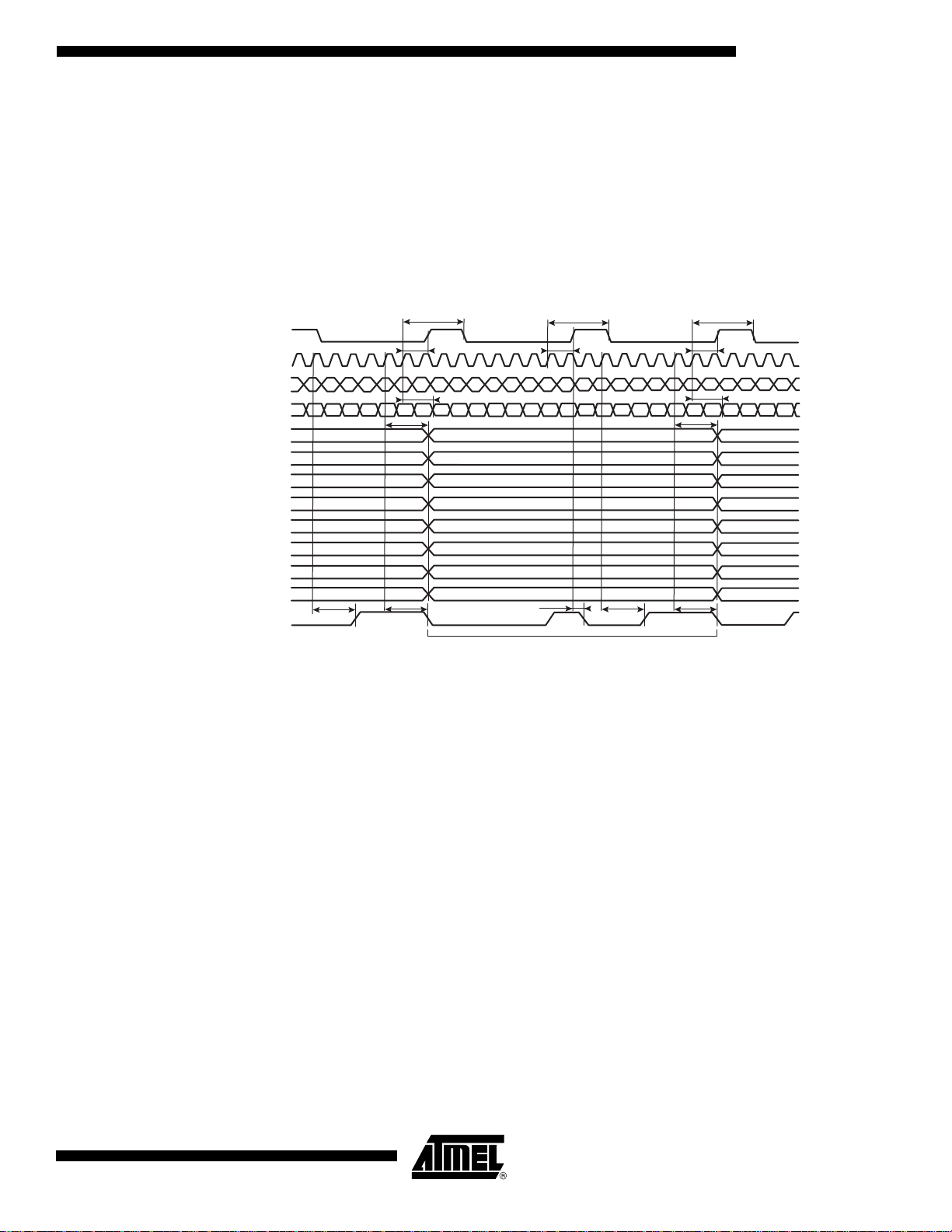
See Timing Diagrams Figure 10 on page 16 to Figure 19 on page 21.
Table 5. Switching Performances
Test
Parameter Symbol
Input Clock
Maximum clock frequency
1:8 ratio
1:4 ratio
Clock pulse width (high) TC1 – 100 – – ps
Clock pulse width (low) TC2 – 100 – – ps
Clock Path pipeline delay
DR input clock
DR/2 input clock
Clock rise/fall time TRCKIN
Asynchronous Reset
Asynchronous Reset pulse width PWAR – 1000 – – ps
Setup time from Asynchronous to Clkln TSAR – – 1500 – ps
Rise/fall time for (10% – 90%) TRAR
FMAX – 2
TCPD
TCPD
TFCKIN
TF AR
Level
1
–––981
– – 100 – ps
– 1000 – – ps
Value
–
–
1084
2.2
1.1
–
–
Unit NoteMin Typ Max
GHz
ps
ps
(1)
(2)
2105C–BDC–11/03
13
Page 14

Table 5. Switching Performances (Continued)
Value
Unit NoteMin Typ Max
Parameter Symbol
Test
Level
Synchronous Reset
Setup time from SyncReset to Clkln
DR input clock
DR/2 input clock
TSSR – –
-580
–
-477
–
–
ps
ps
Hold time from Clkln to SyncReset
DR input clock
DR/2 input clock
THSR – –
780
–
677
–
–
ps
ps
Rise/fall for (10% – 90%) TSRR/TFSR – 100 – – ps
Input Data
Setup time from I[0…9] to Clkln
DR input clock
DR/2 input clock
TSCKIN – –
-794
–
-691
–
–
ps
ps
Hold time from Clkln to I[0…9]
DR input clock
DR/2 input clock
THCKIN – –
994
–
891
–
–
ps
ps
Rise/fall for (10% – 90%) TRDI/TFDI – 100 – – ps
Output Data
Data output delay
DR input clock
DR/2 input clock
TOD – –
1820
–
1717
–
–
ps
ps
(3)
(4)
(5)
(6)
(7)
(8)
(9)
(10)
(11)
(12)
Data pipeline delay
DR input clock, 1:4 ratio
DR input clock, 1:8 ratio
DR/2 input clock, 1:4 ratio
DR/2 input clock, 1:8 ratio
TPD –
–
–
–
–
3
7
3/2
7/2
–
–
–
Number
of input
clock
–
Rise/fall for (10% – 90%) TROD/tfod – – 497/484 – ps
Data Ready
Data ready Falling edge
DR input clock
DR/2 input clock
TDRF – –
1856
–
1753
–
–
ps
ps
Data ready Rising edge
DR input clock
DR/2 input clock
TDRR – –
1828
–
1725
–
–
ps
ps
Asynchr; Reset to DataReady delay TARDR – – 1918 – ps
Synchr. Reset to DataReady delay TSRDR – – 1037 – ps
Rise/fall for (10% – 90%) TRDR/TFDR – – 450 – ps
Rising edge uncertainty JITTER – – 62 – ps
Built-In Self Test
Hold time from Clkln to BIST THBIST – – – – ps
(13)
(14)
(15)
(16)
(17)
(18)
(19)
(20)
(21)
(22)
14
TS81102G0
2105C–BDC–11/03
Page 15

Table 5. Switching Performances (Continued)
TS81102G0
Test
Parameter Symbol
Setup time from Bist to Clkln TSBIST – – 1000 – ps
Rise/fall time for (10% – 90%) TRBIST/
TFBIST
ADC Delay Adjust
Input frequency FMADA – 2 – 2.2 GHz
Input pulse width (high) TC1ADA – 90 – – ps
Input pulse width (low) TC2ADA – 90 – – ps
Input rise/fall time TRIADA/
TFIADA
Output rise/fall time TROADA/
TFOADA
Data output delay (typical delay adjust setting)
Output delay drift with temperature TADAT – – 2.5 – ps/°C
Output delay uncertainly JITADA – – 30 – ps
Notes: 1. TCPD is tuned with DMUXDelAdjCtrl: TCPD = 981 ± 250 ps.
2. TCPD is tuned with DMUXDelAdjCtrl: TCPD = 1084 ± 250 ps.
3. TSSR depends on DMUXDelAdjCtrl: TSSR = -580 ± 250 ps. TSSR < 0 because of Clock Path internal delay.
4. TSSR depends on DMUXDelAdjCtrl: TSSR = -477 ± 250 ps. TSSR < 0 because of Clock Path internal delay.
5. THSR depends on DMUXDelAdjCtrl: THSR = 780 ± 250 ps.
6. THSR depends on DMUXDelAdjCtrl: THSR = 677 ± 250 ps.
7. TSCKIN depends on DMUXDelAdjCtrl: TSCKIN = -794 ± 250 ps. TSCKIN < 0 because of Clock Path internal delay.
8. TSCKIN depends on DMUXDelAdjCtrl: TSCKIN = -691 ± 250 ps. TSCKIN < 0 because of Clock Path internal delay.
9. THCKIN depends on DMUXDelAdjCtrl: THCKIN = 994 ± 250 ps.
10.THCKIN depends on DMUXDelAdjCtrl: THCKIN = 891 ± 250 ps.
11.TOD depends on DMUXDelAdjCtrl: TOD = 1820 ± 250 ps. TOD is given for ECL 50Ω/2 pFoutput load.
12.TOD depends on DMUXDelAdjCtrl: TOD = 1717 ± 250 ps. TOD is given for ECL 50Ω/2 pFoutput load.
13.TPD is the number of Clkln clock cycle from selection of Port A to selection of Port H in 1:8 conversion mode, and from
selection of Port A to selection of Port D in 1:4 conversion mode. It is the maximum number of Clkln clock cycle, or pipeline
delay, that a data has to stay in the DMUX before being sorted out. This maximum delay occurs for the data sent to Port A.
For instance, the data sent to Port H goes directly from the input to the Port H, and its pipeline is 0. Bu t even for this data,
there is an additional delay due to physical propagation time in the DMUX.
14.TROD and TFOD are given for ECL 50Ω/2 pF output load. In TTL mode, the TROD and TFOD are twice the ones for ECL.
(For other termination topology, apply proper derating value 50 ps/pF in ECL, 100 ps/pF in TTL mode.)
15.TDRF depends on DMUXDelAdjCtrl: TDRF = 1856 ± 250 ps. It is given for ECL 50Ω/2 pF output load.
16.TDRF depends on DMUXDelAdjCtrl: TDRF = 1753 ± 250 ps. It is given for ECL 50Ω/2 pF output load.
17.TDRR depends on DMUXDelAdjCtrl: TDRR = 1858 ± 250 ps. It is given for ECL 50Ω/2 pF output load.
18.TDRR depends on DMUXDelAdjCtrl: TDRR = 1725 ± 250 ps. It is given for ECL 50Ω/2 pF output load.
19.TARDR is given for ECL 50Ω/2 pF output load.
20.TSRDR is given for ECL 50Ω/2 pF output load. It is minimum value since RstSync clock is synchronized with Clkln clock.
21.TRDR and TFDR are given for ECL 50Ω/2 pF output load.
22.THBIST depends on the configuration of the DMUX. There must be enough Clkln clock cycles to have all the 512 codes,
(see different Timing Diagrams).
23.With transmission line (ZO = 50Ω) and output load R = 50Ω; C = 2 pF.
24.Without output load.
25.With transmission line (ZO = 50Ω) and output load R = 50Ω; C = 2 pF.
TADA –
Level
– 1000 – – ps
–
–
100
100
–
–
–
–
Value
150
150
145
104
784
896
–
–
–
–
–
–
Unit NoteMin Typ Max
ps
ps
ps
(23)
(24)
(25)
2105C–BDC–11/03
15
Page 16

Input Clock Timings
Figure 10. Input Clock
TC2
TFCKIN
TC1
TRCKIN
Clkln
Data [0..9]
TSCKIN
d1 d2 d3 d4
Clkln Type = 1
DataReady Mode (DR)
THCKIN
ADC Delay Adjust
Timing Diagram
Figure 11. ADC Delay Adjust Timing Diagram
d5
TC2
TFCKIN
TC1
TRCKIN
TSCKIN
d1 d2 d3 d4 d5
Clkln Type = 0
DataReady/2 Mode (DR/2)
THCKIN
TC2ADA
TFIADA
TC1ADA
TRIADA
ADCDelAdjIn
TFOADA
ADCDelAdjOut
TROADA
TADA
16
TS81102G0
2105C–BDC–11/03
Page 17

TS81102G0
Timing Diagrams with
Asynchronous Reset
With a nominal tuning of DMUXDelAdj at a frequency of 2 GHz, d1 and d2 data is lost because
of the internal clock’s path propagation delay TCPD. TCPD is tuned with DMUXDelAdjCt rl pins
to obtain good setup and hold times between Clkln and the da ta.
Figure 12. Start with Asynchronous Rest, 1:8 Ratio, DR Mode
ASyncReset
Clkn
Internal Port Selection
(not available out of the DEMUX)
I[0..9]
A[0..9]
B[0..9]
C[0..9]
D[0..9]
E[0..9]
F[0..9]
G[0..9]
H[0..9]
DR
TRAR
TARDR
PWAR
TFAR
TCPD
ABCD
d1 d2 d3 d4 d5 d6 d7 d8 d9 d10 d11
TDRR
TPD
EFGH BACDEFGH
TOD
TDRF
d12 d13 d14 d15 d16 d17
d3
d4
d5
d6
d7
d8
d9
TRDR TFDR
TOD
TROD/TFOD
d10
d11
d12
d13
d14
d15
d16
d17
With a nominal tuning of DMUXDelAdj at 2 GHz, d1 an d d 2 dat a is lost be ca use of t he int er nal
clock’s path propagation delay TCPD. TCPD is tuned with DMUXDelAdjCtrl pins to obtain
good setup and hold times between Clkln and the input data. This timing diagram does not
change with the opposite phase of Clkln.
Figure 13. Start with Asynchronous Rest, 1:8 Ratio, DR/2 Mode
ASyncReset
Clkn
Internal Port Selection
(not available out of the DEMUX)
I[0..9]
A[0..9]
B[0..9]
C[0..9]
D[0..9]
E[0..9]
F[0..9]
G[0..9]
H[0..9]
DR
TRAR
TARDR
TFAR
PWAR
TCPD
ABCD
d1 d2 d3 d4 d5 d6 d7 d8 d9 d10 d11
TDRR
TPD
TCPD
EFGH BACDEFGH
TOD
TDRF
d12 d13 d14 d15 d16 d17
d3
d4
d5
d6
d7
d8
d9
TRDR TFDR
TOD
TROD/TFOD
d10
d11
d12
d13
d14
d15
d16
d17
2105C–BDC–11/03
17
Page 18

With a nominal tuning of DMUXDelAdj, at 1 GHz (1:4 mode) d1 data is lost because of the
internal clock’s path propagation delay TCPD. TCPD is tuned with DMUXDelAdjCtrl pins and
is used to obtain good setup and hold times between Clkln and the input data.
Figure 14. Start with Asynchronous Reset, 1:4 Ratio, DR Mode
ASyncReset
Clkn
Internal Port Selection
(not available out of the DEMUX)
TRAR
PWAR
TFAR
TCPD
ABCD
TPD
BACD
I[0..9]
A[0..9]
B[0..9]
C[0..9]
D[0..9]
TARDR
DR
d1 d2 d3 d4 d5 d6 d7 d8
TDRR
TRDR
With a nominal tuning of DMUXDelAdj, at 1 GHz (1:4 mode) d1 data is lost because of the
internal clock’s path propagation delay TCPD. TCPD is tuned with DMUXDelAdjCtrl pins and
is used to obtain good setup and hold times betwe en Clkln and the input data. This timing diagram does not change with the opposite phase of Clkln.
Figure 15. Start with Asynchronous Reset, 1:4 Ratio, DR/2 Mode
ASyncReset
Clkn
Internal Port Selection
(not available out of the DEMUX)
TRAR
PWAR
TFAR
TCPD
A
B
TOD
TDRF TDRR
TFDR
TCPD
CD
TPD
d2
d3
d4
TOD
d5
d6
d7
d8
TROD/TFOD
BA C
18
I[0..9]
A[0..9]
B[0..9]
C[0..9]
D[0..9]
DR
TS81102G0
TARDR
d1 d2 d3 d4 d5 d6 d7 d8
TOD
d5
d6
d7
d8
TROD/TFOD
TDRR
TRDR
TOD
d2
d3
d4
TDRF
TFDR
2105C–BDC–11/03
Page 19
TS81102G0
Timing Diagrams with
Synchronous Reset
Following is an example of the Synchronous Reset’s utility in case of de-synchronization of the
DMUX output port selection. The de-synchronization event happens after the selection of Port
D.
DMUXDelAdjCtrl value is nominal. TSSR < 0 because of Clkln’s internal propagation delay
TCPD. After selection of Port C, instead of selecting Por t D, t he de -synchronization makes the
port selection to restart on Port A. Since Port H was not selected, the data is not output to the
ports but the last data (d1 to d 8) is latc hed unt il t he ne xt sel ectio n of Por t H. d9 to d16 ar e lo st .
The synchronous Reset ensures a re-synchronization of the port selection.
Figure 16. Synchronous Reset, 1:8 Ratio, DR Mode
SyncReset
Clkn
I[0..9]
Internal Port Selection
(not available out of the DEMUX)
A[0..9]
B[0..9]
C[0..9]
D[0..9]
E[0..9]
F[0..9]
G[0..9]
H[0..9]
DR
d1d0 d2 d3 d4 d5 d6 d7 d8 d9 d10 d11
ABCD
TDRR
TSSR
EDEFGH BACBAC DEFGHBAC DBA C
TOD
TDRF TDRR TDRF
TCPD
THSR
THSR
TSSR
d12 d13 d14 d15 d16 d17 d18 d19 d20 d21 d22 d23 d24 d25 d26 d27
d2
TSRDR
THSR
TSSR
TCPD
TOD
d17d1
d18
d19d3
d20d4
d21d5
d22d6
d23d7
d24d8
Period of uncertainty due to desynchronization
Example of the Synchronous Reset’s utility in case of de-synchronization of the DMUX output
port selection. The de-synchronization event happens after the selection of Port D.
DMUXDelAdjCtrl value is nominal. TSSR < 0 because of Clkln’s internal propagation delay
TCPD. After selection of Port C, instead of selecting Por t D, t he de -synchronization makes the
port selection to restart on Port A. Since Port H was not selected, the data is not output to the
ports but the last data (d1 to d4) is latched until the next selection of Port H. d5 to d8 are lost.
The synchronous Reset ensures a re-synchronization of the port selection.
2105C–BDC–11/03
19
Page 20

Figure 17. Synchronous Reset, 1:4 Ratio, DR Mode
SyncReset
Clkn
I[0..9]
Internal Port Selection
(not available out of the DEMUX)
A[0..9]
B[0..9]
C[0..9]
D[0..9]
d1 d2 d3 d4 d5 d6 d7 d8 d9 d10 d11
DR
Example of Synchronous Reset’s utility in case of de-synchronization of the DMUX output port
selection. The de-synchronization event happens after the selection of Port D.
DMUXDelAdjCtrl value is nominal. TSSR < 0 because of Clkln’s internal propagation delay
TCPD. After selection of Port C, instead of selecting Por t D, t he de -synchronization makes the
port selection to restart on Port A. Since Port H was not selected, the data is not output to the
ports but the last data (d1 to d 8) is latc hed unt il t he ne xt sel ectio n of Por t H. d9 to d16 ar e lo st .
The synchronous Reset ensures a re-synchronization of the port selection.
THSR
TSSR
TCPD
d12 d13 d14 d15
ABCD BCDAB CDAB CD
d1
d2
d3
d4
Period of uncertainty due to desynchronization
TOD
d9
d10
d11
d12
TDRF TDRR
d16
Figure 18. Synchronous Reset, 1:8 ratio, DR/2 Mode
SyncReset
Clkn
I[0..9]
Internal Port Selection
(not available out of the DEMUX)
A[0..9]
B[0..9]
C[0..9]
D[0..9]
E[0..9]
F[0..9]
G[0..9]
H[0..9]
DR
d1d0 d2 d3 d4 d5 d6 d7 d8 d9 d10 d11
ABCD
TOD
TSSR
TCPD
EDEFGH BACBAC DEFGHBAC DBA C
TDRF
Example of Synchronous Reset’s utility in case of de-synchronization of the DMUX output port
selection. The de-synchronization event happens after the selection of Port D.
DMUXDelAdjCtrl value is nominal. TSSR < 0 because of Clkln’s internal propagation delay
TCPD. After selection of Port C, instead of selecting Por t D, t he de -synchronization makes the
port selection to restart on Port A. Since Port H was not selected, the data is not output to the
ports but the last data (d1 to d4) is latched until the next selection of Port H. d5 to d8 are lost.
The synchronous Reset ensures a re-synchronization of the port selection.
THSR
THSR
TSRR
d12 d13 d14 d15 d16 d17 d18 d19 d20 d21 d22 d23 d24 d25 d26 d27
d1
d2
TSDRR
Period of uncertainty due to desynchronization
TDRR
THSR
TSRR
TCPD
TDRF
TOD
d17
d18
d19d3
d20d4
d21d5
d22d6
d23d7
d24d8
20
TS81102G0
2105C–BDC–11/03
Page 21

TS81102G0
Figure 19. Synchronous Reset, 1:4 ratio, DR/2 Mode
SyncReset
Clkn
I[0..9]
Internal Port Selection
(not available out of the DEMUX)
A[0..9]
B[0..9]
C[0..9]
D[0..9]
d1 d2 d3 d4 d5 d6 d7 d8 d9 d10 d11
ABCD BC AABCDABCD
DR
Period of uncertainty due to desynchronization
Note: In case of low clock frequency and start with asynchronous reset, o nly the first data is lost and the fi rst data to b e pro cessed is
the second one. This data is output from the DMUX through port B.
TSSR
TCPD
d1
d2
d3
d4
THSR
TOD
TDRF
d12 d13 d14 d15
d9
d10
d11
d12
TDRR
d16
2105C–BDC–11/03
21
Page 22

Explanation of
Test Levels
Table 6. Explanation of Test Levels
Num Characteristics
(1)
1 100% production tested at +25
2 100% production tested at +25°C, and sample tested at specified temperatures.
3 Sample tested only at specified temperatures.
4
5 Parameter is a typical value only.
Notes: 1. The level 1 and 2 tests are performed at 50 MHz.
Parameter is guaranteed by design and characterization testing (thermal steady-state
conditions at specified temperature).
2. Only MIN and MAX values are guaranteed (typical values are issuing from characterization
results).
°C.
(1)
22
TS81102G0
2105C–BDC–11/03
Page 23
TS81102G0
Package Description
Pin Description
Table 7. TS81102G0 Pin Description
Type Name Levels Comments
Digital Inputs I[0…9] Differential ECL Data input.
On-chip 100Ω differential termination resistor.
Clkln Differential ECL Clock input (Data Ready ADC).
On-chip 100Ω differential termination resistor.
Outputs A[0…9] → H[0…9] Adjustable Logic
Single
DR Adjustable Logic
Differential
RefA → RefH Adjustable Single Reference voltage for output channels A to H.
Control Signals ClklnType TTL DataReady or Dataready/2: logic 1: Data Ready.
RatioSel TTL DMUX ratio; logic 1: 1:4
Data ready for port A to H.
Common mode is adjusted with VplusDOut. Swing is adjusted with
SwiAdj. 50Ω termination possible.
Data ready for channel A to H.
Common mode is adjusted with VplusDOut. Swing is adjusted with
SwiAdj. 50Ω termination possible.
Common mode is adjustable with VplusDOut. 50Ω termination
possible.
Bist TTL Reset and Switch of built-in Self Test (BIST): logic 0: BIST active.
SwiAdj 0V ± 0.5V Swing fine adjustment of output buffers.
Diode Analog Diode for chip temperature measurement.
NbBit TTL Number of bit 8 or 10: logic 1: 10-bit.
Synchronization AsyncReset TTL Asynchronous reset: logic 1: reset on.
SyncReset Differential ECL Synchronous reset: active on rising edge.
DMUXDelAdjCtrl Differential analog
input of ±0.5V
around 0V
common mode
ADCDelAdjCtrl Differential analog
input of ±0.5V
around 0V
common mode
ADCDelAdjln Differential ECL Stand-alone delay adjust input for ADC.
ADCDelAdjOut 50Ω differential
output
Power Supplies GND Ground 0V Common ground.
V
EE
V
PlusDOut
V
CC
Power -5V Digital negative power supply.
Adjustable power
from 0V to +3.3V
Power +5V Digital positive power supply.
Control of the delay line of DataReady input:
differential input = -0.5V: delay = 250 ps
differential input = 0V: delay = 500 ps
differential input = 0.5V: delay = 750 ps
Control of the delay line for ADC:
differential input = - 0.5V: delay = 250 ps
differential input = 0V: delay = 500 ps
differential input = 0.5V: delay = 750 ps
Differential termination of 100Ω inside the buffer.
Stand-alone delay adjust output for ADC.
Common mode adjustment of output buffers.
2105C–BDC–11/03
23
Page 24

TBGA 240 Package – Pinout
Row Col Name Row Col Name Row Col Name Row Col Name
VEE
17
A
A
A
A
A
A
A
A
A
A
A
A
A
A
A
A
A
A
A
B
B
B
B
B
B
B
B
B
B
B
B
B
B
B
B
B
B
B
C
C
C
C
C
C
C
C
C
C
C
C
C
C
C
C
C
C
C
D
D
D
E3
2
E5
3
E7
4
E9
5
C0
6
C2
7
C4
8
C6
9
C8
10
REFA
11
A1
12
A3
13
A5
14
A7
15
A9
16
DEMUXDELADJCTRL
17
RSTSYNCB
18
NC
19
E1
1
E2
2
E4
3
E6
4
E8
5
REFC
6
C1
7
C3
8
C5
9
C7
10
C9
11
A0
12
A2
13
A4
14
A6
15
A8
16
ASYNCRESET
17
DEMUXDELADJCTRLB
18
RSTSYNC
19
REFE
1
E0
2
VEE
3
VPLUSDOUT
4
VPLUSDOUT
5
VPLUSDOUT
6
VPLUSDOUT
7
VEE
8
VPLUSDOUT
9
VEE
10
VPLUSDOUT
11
VEE
12
VPLUSDOUT
13
VPLUSDOUT
14
VPLUSDOUT
15
GND
16
GND
17
GND
18
DIODE
19
G8
1
G9
2
VEE
3
NC
1
D
D
D
D
D
D
D
D
D
D
D
D
D
D
D
D
E
E
E
E
E
E
E
E
F
F
F
F
F
F
F
F
G
G
G
G
G
G
G
G
H
H
H
H
H
H
H
H
J
J
J
J
J
J
J
J
K
K
K
K
VEE
5
VPLUSDOUT
6
VPLUSDOUT
7
VEE
8
VPLUSDOUT
9
VEE
10
VPLUSDOUT
11
VEE
12
VPLUSDOUT
13
GND
14
VCC
15
VCC
16
GND
17
I0B
18
I0
19
G6
1
G7
2
VPLUSDOUT
3
VEE
4
VEE
16
VEE
17
I1B
18
I1
19
G4
1
G5
2
GND
3
GND
4
GND
16
GND
17
I2B
18
I2
19
G2
1
G3
2
VEE
3
VEE
4
VEE
16
VEE
17
I3B
18
I3
19
G0
1
G1
2
GND
3
GND
4
GND
16
GND
17
CLKINB
18
CLKIN
19
DR
1
REFG
2
VPLUSDOUT
3
VCC
4
VEE
16
VEE
17
I4B
18
I4
19
SWIADJ
1
DRB
2
VEE
3
VEE
4
VEE
4
K
K
K
K
L
L
L
L
L
L
L
L
M
M
M
M
M
M
M
M
N
N
N
N
N
N
N
N
P
P
P
P
P
P
P
P
R
R
R
R
R
R
R
R
T
T
T
T
T
T
T
T
T
T
T
T
T
T
T
T
GND
17
I5B
18
I5
19
H9
1
RATIOSEL
2
VPLUSDOUT
3
VPLUSDOUT
4
VEE
16
VEE
17
I6B
18
I6
19
H7
1
H8
2
GND
3
GND
4
GND
16
GND
17
I7B
18
I7
19
H5
1
H6
2
VPLUSDOUT
3
VPLUSDOUT
4
VEE
16
VEE
17
I8B
18
I8
19
H3
1
H4
2
GND
3
GND
4
GND
16
GND
17
I9B
18
I9
19
H1
1
H2
2
VPLUSDOUT
3
VPLUSDOUT
4
VEE
16
GND
17
ADCDELADJOUT
18
ADCDELADJOUTB
19
REFH
1
H0
2
VEE
3
VEE
4
VEE
5
VPLUSDOUT
6
VPLUSDOUT
7
VEE
8
VPLUSDOUT
9
VEE
10
VPLUSDOUT
11
VEE
12
VPLUSDOUT
13
VPLUSDOUT
14
GND
15
VEE
16
VEE
16
T
T
T
U
U
U
U
U
U
U
U
U
U
U
U
U
U
U
U
U
U
U
V
V
V
V
V
V
V
V
V
V
V
V
V
V
V
V
V
V
V
W
W
W
W
W
W
W
W
W
W
W
W
W
W
W
W
W
W
W
ADCDELADJIN
18
ADCDELADJINB
19
F8
1
F9
2
VEE
3
VPLUSDOUT
4
VPLUSDOUT
5
VPLUSDOUT
6
VPLUSDOUT
7
VEE
8
VPLUSDOUT
9
VEE
10
VPLUSDOUT
11
VEE
12
VPLUSDOUT
13
VPLUSDOUT
14
VPLUSDOUT
15
GND
16
GND
17
GND
18
GND
19
F7
1
F6
2
F4
3
F2
4
F0
5
D9
6
D7
7
D5
8
D3
9
D1
10
REFD
11
B8
12
B6
13
B4
14
B2
15
B0
16
BIST
17
CLKINTYPE
18
ADCDELADJCTRL
19
NC
1
F5
2
F3
3
F1
4
REFF
5
D8
6
D6
7
D4
8
D2
9
D0
10
B9
11
B7
12
B5
13
B3
14
B1
15
REFB
16
NBBIT
17
ADCDELADJCTRLB
18
NC
19
24
TS81102G0
2105C–BDC–11/03
Page 25

Figure 20. TBGA 240 Package: Bottom View
19181716151413121110987654321
TS81102G0
RstSyncb
RstSync
Demuxdeladjctrclb
DIODE
GND
I0
I0b
I1b
I1
I2b GND GND
I2
I3 I3b
CLK CLKb
I4b
I4
I5
I5b
I6b
I6
I7b
I7
I8b
I8
Demuxdeladjctrcl
Asyncreset
GND
GND
VEE VEE
VEE VEE
GND GND
VEE VEE
GND VEE
VEE VEE
GND
VEE VEE
C8A1
A0 C9
VEE
VEE
REFA
VPLUSD
VPLUSD
C6
C7
C5 C3 E6
VPLUSD
VEE
VPLUSD
VEE
A9 A5A7
A3
A4A8 A6 A2
VPLUSD
VPLUSD
GND
VCC VCC VEE
GND
VPLUSD
VPLUSD
C4
VEE
VEE
C2
C1
VPLUSD
VPLUSD
C0
REFC
VPLUSD
VPLUSD
E9
E8
VPLUSD
VEE
VPLUSD
VEE
GND GND
VEE
GND GND
VCC
VEE VEE
VPLUSD
GND
GND GND
VPLUSD VPLUSD
E5 E3E7
E4
VEE
VEE
VPLUSD
VEE
VPLUSD
VPLUSD
E2 E1
E0
G9 G8
G7 G6
G5 G4
G1 G0
REFG
DRb
RATIOSEL
H8 H7
H6
REFE
G2G3
DR
SWIadj
H9
H5
A
B
C
D
E
F
G
H
J
K
L
M
N
I9
GND
ADCDELADJCTRL
ADCDELADJCTRLb
2105C–BDC–11/03
I9b
ADCdelayadjoutADCdelayadjoutB
ADCdelayadjinADCdelayadjinB
GND
CLKINTYPE
GND
GND
VEE
GND
BIST
NbBIT
GND
VEE
VEE
GND
B0
REFB
GND
VPLUSD
B2
VPLUSD
VPLUSD
B4
B3B1 B5
VPLUSD
VPLUSD
B6
VEE
VEE
B8
VPLUSD
VPLUSD
REFD
VEE
VEE
D1
VPLUSD
VPLUSD
D3
VEE
VEE
VPLUSD
VPLUSD
D7D5
VPLUSD
VPLUSD
D9 F0
VEE
VPLUSD
REFF
GND
VPLUSD
VEE
VPLUSD
F2
F1B9B7 D0 D2 D6D4 D8
GND
VPLUSD
VEE
VEE
F4
F3 F5
H4
H3
H2
H1
REFH
H0
F9
F8
F7F6
P
R
T
U
V
W
25
Page 26
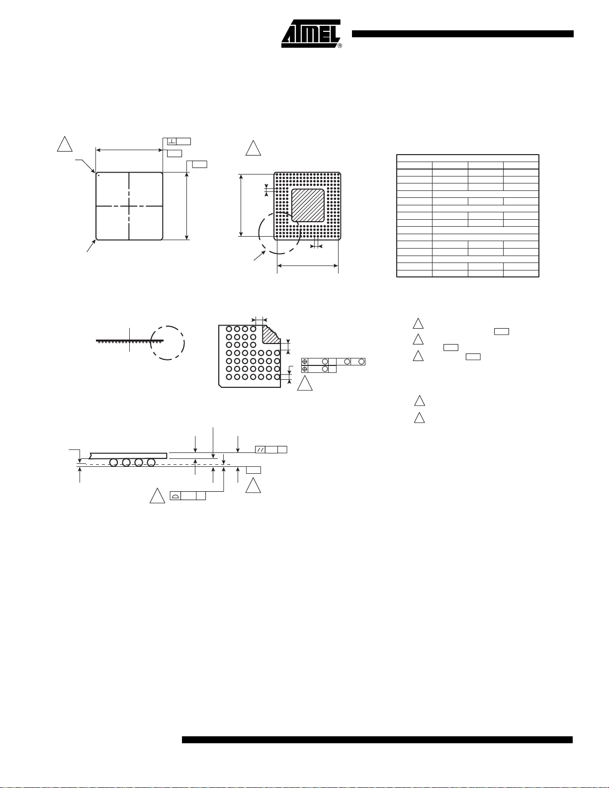
Outline
Dimensions
Figure 21. Package Dimension – 240 Tape Ball Grid Array
11
Corner
45 degree
0.5 mm chamfer
(4 PLCS)
P
D
Top View
Detail A
Side View
0.10
- A -
- B -
E E1
C
10
18
e
Detail B
D1
Bottom View
g
g
b
4
Detail B
A1
A
ccc C
e
0.30
M M M
M
0.30
1
35791113151719
246810121416
A
C
E
G
J
L
N
R
U
W
A
C B
C
Dimensional References
Ref.
B
D
F
H
K
M
P
T
V
A
A1
D
D1
E
E1
b
c
M
N
aaa
ccc
e
g
P
Notes: 1. All dimensions are in millimeters.
Min.
1.30
0.50
24.80
24.80
0.60
0.80
-
-
0.35
0.15
2. "e" represents the basic solder ball grid pitch.
3. "M" represents the basic solder ball matrix size,
and symbol "N" is the maximum allowable number
of balls after depopulating.
4 "b" is measured at the maximum solder ball diameter
parallel to primary datum - C -
5 Dimension "aaa" is measured parallel to primary
datum - C -
6 Primary datum - C - and seatin plane are defined by
the spherical crowns of the solder balls.
7. Package surface shall be black oxide.
8. Cavity depth various with die thickness.
9. Substrate material base is copper.
10
Bilateral tolerance zone is applied to each side of
package body.
11
45 deg. 0.5 mm chamfer corner and white dot for
pin 1 identification.
Nom.
1.50
0.60
25.00
22.86 (BSC.)
25.00
22.86 (BSC.)
0.75
0.90
19.00
240.00
---
-
1.27 TYP.
-
-
Max.
1.70
0.70
25.20
25.20
0.90
1.00
0.15
0.25
-
-
Detail A
Thermal and Moisture
Characteristics
Thermal Resistance
from Junction to
Case: RTHJC
26
TS81102G0
- C -
aaa
5
C
6
The Rth from junction to case for th e TBGA package is estimated at 1.05 °C/W that ca n be broken down as follows:
• Silicon: 0.1°C/W
• Die attach epoxy: 0.5°C/W (thickness # 50 µm)
• Copper block (back side of the package): 0.1°C/W
• Black Ink: 0.251°C/W.
2105C–BDC–11/03
Page 27
TS81102G0
Thermal Resistance
from Junction to
Ambient: RTHJA
A pin-fin type heat sink of a size 40 mm x 40 mm x 8 mm can be used to r edu ce ther ma l re si stance. This heat sink should not be glued to the t op of the pa ckage as Atmel cannot guar antee
the attachment to the board in such a configurat ion. The h eat sink could be clip ped or screwed
on the board.
With such a heat sink, the Rthj-a is about 6°C/W (if we take 10°C/W for Rth from the junction
to air through the package and heat sink in para llel with 15°C/W from the junction to the board
through the package body, through balls and thr ough board copper).
Without the heat sink, the Rth junction to air for a p ackage reported on-board can be estimated
at 13 to 20°C/W (depending on the board used).
The worst value 20°C/W is given for a 1-layer board (13°C for a 4-layer board).
Thermal Resistance
from Junction to
Bottom of Balls
The thermal resistance from the junction to the bottom of the balls of the package corresponds
to the total thermal resistance to be considered from the silicon’s die junction to the interface
with a board. This thermal resistance is estimated to be 4.8°C/W max.
The following diagram points out how the previous thermal resistances were calcula ted for this
packaged device.
Figure 22. Thermal Resistance from Junction to Bottom of Balls
DEMUX − Axpproximative Model for 240 TBGA
Assumptions:
Square die 7.0 x 7.0 = 49 mm², 75 µm thick Epoxy/Ag glue, 0.40 mm copper thickness under die,
Sn60Pb40 columns diameter 0.76 mm, 23 x 23 mm TBGA
Typical values
(values are in °C/Watt)
Silicon Die
49 mm²
λ = 0.95Watt/°C
Epoxy/Ag glue
λ = 0.025Watt/°C
(Top half of thickness)
Copper base
λ = 25Watt/°C
Copper base
Black ink
Thermal Resistance Junction to case typical =
0.10 + 0.60 + 0.05 + 0.05 + 0.25 = 1.05°C/W
Thermal Resistance Junction to case Max = 1.40°C/W
0.10
0.60
0.05
0.05
0.25
Top of
package
1.87
0.40
2 internal
rows
(104 balls)
0.251.70
2 external
(136 balls)
rows
1.43
0.31
Tape + glue
over balls
λ = 0.02Watt/°C
Balls
PbSn
λ = 0.40Watt/°C
Case were all Bottom of Balls are connected to infinite heatsink
(values are in °C/Watt)
Silicon JunctionSilicon Junction
0.10
0.60
0.05
Infinite heatsink
at bottom of balls
Thermal Resistance Junction to bottom of balls = 4.8°C/W Max
Reduction
Silicon
0.251.70
2.47 1.74 1.99
Junction
Infinite heatsink
at bottom of balls
Reduction
Silicon
Junction
2.45
3.55
2.47
Infinite heatsink
at bottom of balls
2105C–BDC–11/03
27
Page 28

Temperature Diode
Characteristic
The theoretical characteristic of the diode according to the temperature when I = 3 mA is
depicted below.
Figure 23. Temperature Diode Characteristic
Moisture
Characteristic
Vdiode
1.0
900m
(V)
800m
700m
-70.0 -20.0 30.0 80.0
DiodeT
I = 3 mA
dV/dT = 1.32 mV/°C
130.0
Temperature (°C)
This device is sensitive to moisture (MSL3 according to the JEDEC standard).
The shelf life in a sealed bag is 12 months at < 40°C and < 90% relative humidity (RH).
After this bag is opened, devices that might be subjected to infrared reflow, vapor-phase
reflow, or equivalent processing (peak package body temperature 220°C) must be:
• mounted within 168 hours at factory conditions of ≤ 30°C/60% RH, or
•stored at ≤ 20% RH.
28
The devices require baking before mounting, if the humidity indicator is > 20% when read at
23°C ±5°C.
If baking is required, the devices may be baked for:
• 192 hours at 40°C + 5°C/-0°C and < 5% RH for low temperature device containers, or
• 24 hours at 125°C ± 5°C for high-temperature device containers.
TS81102G0
2105C–BDC–11/03
Page 29
TS81102G0
Detailled Cross
The following diagram depicts a detailed cross sectio n of the DM UX TBG A packa ge .
Section
Figure 24. TBGA 240: 1/2 Cross Section
Die Attach Epoxy/Ag
Silicon Die
Block Epoxy resin
encapsulant
In the DMUX package shown above, the die’s rear side is attached to the copper heat
spreader, so the copper heat spreader is at -5V.
Gold
wires
Copper Heatspreader
Copper traces
and
Solder Balls Pads
on metal 1 side
Block overcoat
Sn/Pb/Ag
62/36/2 Eutectic
Solder Balls
Adhesive
Solder Mask
Metal 2 side
Polyimide Tape
Solder Mask
Metal 1 side
It is necessary to use a heat sink tied to the copper heat speader.
Moreover, there is only a little layer of painting over the copper heat spreader which does not
isolate it.
It is therefore recommended to either isolate the heat sink from the other components of the
board or to electrically isolate the copper heat spreader from the heat sink. In the latter case,
one should use adequate low Rth electrical isolation.
2105C–BDC–11/03
29
Page 30
Applying the
TS81102G0
DMUX
The TSEV81102G0 DMUX evaluation board is designed to be connected with the
TSEV8388G and TSEV83102G0 ADC evaluation boards.
Figure 25. TSEV81102G0 DMUX Evaluation Boards
VplusD = 0V → 3.3V
CLOCK
BUFFER
Clkln
Analog
Input
ADC
Data
Bus
Data
Ready
8bits 1 GHz TS8388B
10bits 2 GHz TS83102G0
s-e or diff.
(2 GHz)
(1 GHz)
8b/10b diff.
(1 - 2 GHz)
1b diff.
ECL
Rload = 50Ω
Vih = -1.0V
Vil = -1.4V
FS
Vcc = +5V
I[0..9]
Clkln
Delay
adjust
control
DEMUX
delay
Number
of bits
(8/10)
Vee = -5V
A[0..9] → H[0..9]
Synchronous or
Asynchronous
TS81102G0
RefA → RefH
DR
Reset
(125 MHz)
8x8b/10b single
(DC)
8 ref
(250 MHz)
1b diff.
ECL + ref
VplusD = ground
Rload = 50Ω
Vtt = -2V
Voh = -0.8V
Vol = -1.8V
TTL + ref
VplusD = 3.3V
Rload ≥ 75Ω
Vtt = ground
Voh = 2.5V
Vol = 0.5V
PECL + ref
VplusD = 3.3V
Rload = 50Ω
Vtt = 1.3V
Voh = 2.5V
Vol = 1.5V
ASIC
30
Please refer to the "ADC and DMUX Application Note" for more information.
TS81102G0
2105C–BDC–11/03
Page 31

TS81102G0
ADC to DMUX
Connections
The DMUX inputs configuration has been optimized to be connected to the TS8388B ADC.
The die in the TBGA package is up. For the ADC, different types of packages can be used
such as CBGA with die up or the CQFP68 down. The DMUX device being completely symmetrical, both ADC packages can be connected to the TBGA pa ckage of the DMUX crisscrossing the lines (see Table 8).
Table 8. ADC to DMUX Connections
ADC Digital Outputs
CQFP68 Package
D0 I7 D0 I0
D1 I6 D1 I1
D2 I5 D2 I2
D3 I4 D3 I3
D4 I3 D4 I4
D5 I2 D5 I5
D6 I1 D6 I6
D7 I0 D7 I7
– 18 not connected – 18 not connected
– 19 not connected – 19 not connected
DMUX Data Inputs
TBGA Package
ADC Digital Outputs
CBGA Package
DMUX Data Inputs
TBGA Package
Note: The connection between the ADC evaluation board and the DMUX evaluation board requires a
4-pin shift to make the D0 pin match either the I7 or I0 pin of the DMUX evaluation board.
2105C–BDC–11/03
31
Page 32

TSEV81102G0TP: Device Evaluation Board
General
Description
The TSEV81102G0TP DMUX Evaluation Board (EB) is designed to simplify the characterization and the evaluation of the TS81102G0 device (2 Gsps DMUX). The DMUX EB enables
testing of all the DMUX functions: Synchronous and Asynchronous reset functions, selection
of the DMUX ratio (1:4 or 1:8), selection of the number of bits (8 or 10), output data common
mode and swing adjustment, die junction temperature measurements over military temperature range, etc.
The DMUX EB has been designed to enable easy connection to Atme’s ADC Evaluation
Boards (such as TSEV8388BGL or TSEV83102G0BGL) for an extended functionality evaluation (ADC and DMUX multi-channel applications).
The DMUX EB comes fully assembled and tested, with a TS81102G0 device implemented on
the board and a heat sink assembled on the device.
32
TS81102G0
2105C–BDC–11/03
Page 33

TS81102G0
Ordering
Information
Table 9. Ordering Information
Part Number Package Temperature Range Screening Comments
JTS81102G0-1V1A Die Ambient Visual inspection
TS81102G0CTP TBGA 240 "C" grade
0°C < Tc; Tj < 90°C
TS81102G0VTP TBGA 240 "V" grade
-40°C < Tc; Tj < 110°C
TSEV81102G0TPZR3 TBGA 240 Ambient Prototype Evaluation board (delivered
Datasheet
Standard
Standard
with heatsink)
Status
Description
Table 10. Datasheet Status
Datasheet Status Validity
Objective specification This datasheet contains target and
goal specifications for discussion with
customer and application validation.
Target specification This datasheet contains target or
goal specifications for product
development.
Preliminary specificati on
α-site
Preliminary specificati on
β-site
Product specification This datasheet contai ns final product
Limiting Values
Limiting values given are in accordance with the Absolute Maximum Rating System (IEC 134). Stress
above one or more of the limiting values may cause permanent damage to the device. These are
stress ratings only and operation of the device at these or at any other conditions above those given in
the Characteristics sections of the specification is not implied. Exposure to limiting values for extended
periods may affect device reliability.
Application Information
This datasheet contains preliminary
data. Additional data may be
published later; could include
simulation results.
This datasheet contains also
characterization results.
specification.
Before design phase
Valid during the design phase
Valid before characterization
phase
Valid before the
industrialization phase
Valid for production purposes
Life Support
Applications
2105C–BDC–11/03
Where application information is given, it is advisory and does not form part of the specification.
These products are not designed for use in life-support appliances, devices or systems where
malfunction of these products can reasonably be expected to result in person al injury. Atmel
customers using or selling these products for use in such applications do so at their own risk
and agree to fully indemnify Atmel for any damages resulting from such improper use or sale.
33
Page 34

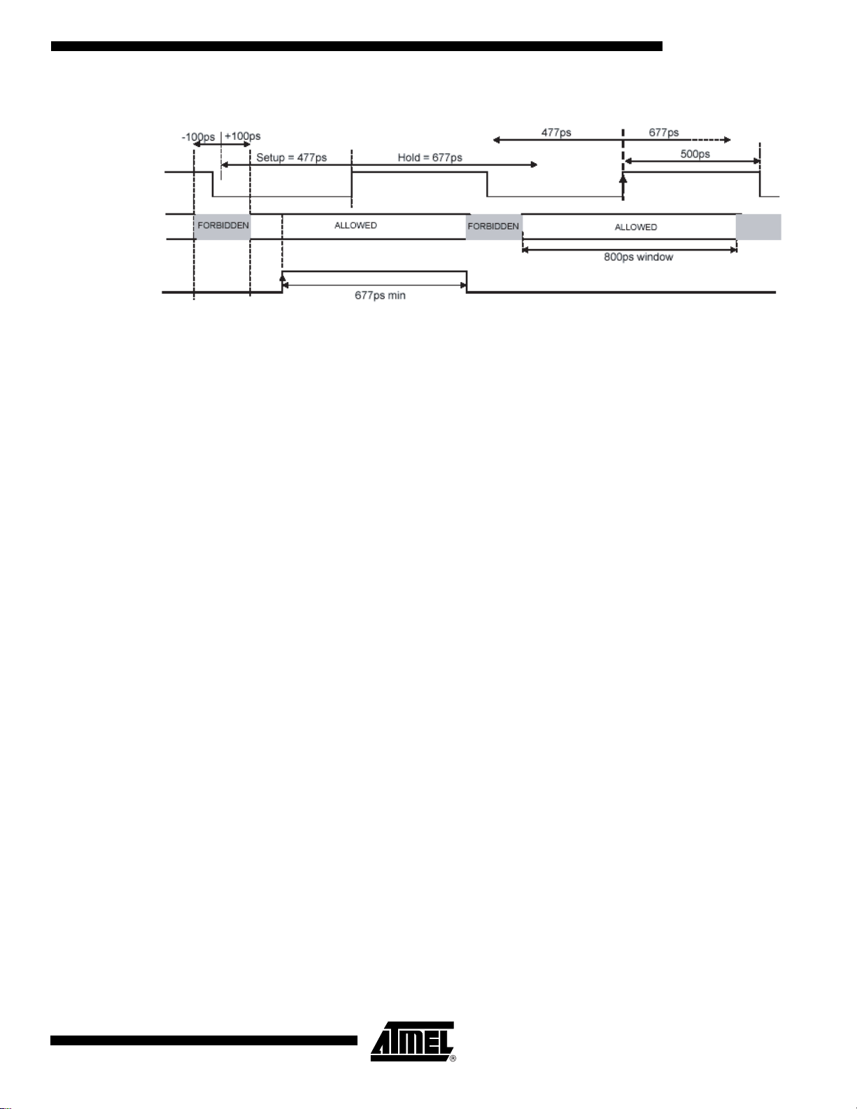
Addendum This section has been added to the description of the device for better understanding of the
synchronous reset operation. It puts particular stress on the setup and hold times defined in
the switching characteristics table (Table 5), linked with the device performances when used
at full speed (2 Gsps).
Synchronous
Reset Operation
SETUP and HOLD
Timings
It first describes the operation of the synchron ous reset in case the DMUX is used in DR mode
and then when used in the DR/2 mode.
As a reminder, the synchronous reset has to be a signal frequency of Fs/8N in 1:8 ratio or
Fs/4N in 1:4 ratio, where N is an integer.
The effect of the synchronous reset is to ensure that at each new port selection cycle, the first
port to be selected is port A. The synchronous reset ensures the internal cyclic synchronization of the device during operation. It is also highly recommended in the case of multichannel
applications using 2 synchronized DMUXs.
The setup and hold times for the reset are defined as follows:
• SETUP from SynchReset to Clkin:
Required delay between the rising edge of the reset and the rising edge of the clock to ensure
that the reset will be taken into account at the next clock edge. If the reset rising edge occurs
at less than this setup time, it will be taken into account only at the second next rising edge of
the clock.
A margin of ± 100ps has to be added to this setup time to compensate for the delays from the
drivers and lines.
• HOLD from Clkin and SynchReset:
Minimum duration of the reset signal at a high level to be taken int o account by the DMUX.
This means that the reset signal has to s atisfy 2 requ iremen ts: a frequ ency of Fs/8 N or Fs/4N
(N is an integer) depending on the ratio and a duty cycle such that it is high during at least the
hold time.
Operation in DR Mode In DR mode, the DMUX input clock can run at up to 2 GHz in 1:8 ratio or 1 GHz in 1:4 ratio.
Both cases are described in the following timing diagrams.
Figure 26. Synchronous Reset Operation in DR Mode, 1:4 ratio, 1GHz (Full Speed) – Principle of Operation
Fs
Sync_RESET
34
TS81102G0
2105C–BDC–11/03
Page 35

TS81102G0
Figure 27. Synchronous Reset Operation in DR Mode, 1:4 ratio, 1GHz (Full Speed) – TIMINGS
Fs
Time Zones
Allowed for
the reset
Sync_RESET
Note: The clock edge to which the reset applies is the one identified by the arrow.
If the reset rising edge had occurred in the second allowed window, the reset would have been effective on the third clock rising edge (not
represented, on the right of the edge represented with the arrow).
Figure 28. Synchronous Reset Operation in DR Mode, 1:8 ratio, 2 GHz (Full-speed) – Principle of Operation
Fs
Sync_RESET
Figure 29. Synchronous Reset Operation in DR Mode, 1:8 rati o, 2 GHz (Full-speed) – Timings
Fs
Times Zones
Allowed for
the reset
Sync_RESET
Note: The clock edge to which the reset applies is the one identified by the arrow.
If the reset rising edge had occurred in the second allowed window, the reset would have been effective on the fourth clock
rising edge (last clock rising edge, on the right of the edge re presented with the arrow).
This case is the most critical one with only a 300 ps window for the reset.
2105C–BDC–11/03
35
Page 36
Operation in DR/2
Mode
In DR/2 mode, the DMUX input clock can run at up to 1 GHz in 1:8 ratio or 500 MHz in 1:4
ratio, since the DR/2 clock from the ADC is half the sampling frequency.
Both cases are described in the following timing diagrams.
Figure 30. Synchronous Reset Operation in DR/2 Mode, 1:4 ratio, 500MHz (Full Speed) – Principle of Operation
Fs/2
Sync_RESET
Figure 31. Synchronous Reset Operation in DR/2 Mode, 1:4 ratio, 500 MHz (Full-speed) – Timings
Fs/2
Times Zones
Allowed for the
reset
Sync_RESET
Note: The clock edge to which the reset applies is the one identified by the arrow.
If the reset rising edge had occurred in the first allowed window (on the le ft) , the re set w ould have been effective on the fi rst
represented clock rising edge (first clock rising edge of the schematic, on the left of the edge represented with the arrow).
Figure 32. Synchronous Reset Operation in DR/2 Mode, 1:8 ratio, 1GHz (Full Speed) – Principle of Operation
Fs/2
Sync_RESET
36
TS81102G0
2105C–BDC–11/03
Page 37
TS81102G0
Figure 33. Synchronous Reset Operation in DR/2 Mode, 1:8 ratio, 1GHz (Full-speed) – Timings
Fs/2
Times Zones
Allowed for the
reset
Sync_RESET
Note: The clock edge to which the reset applies is the one identified by the arrow.
If the reset rising edge had occurred in the second allowed window, the reset would have been effective on the fourth clock rising edge
(not represented, on the right of the edge represented with the arrow).
2105C–BDC–11/03
37
Page 38

Atmel Headquarters Atmel Operations
Corporate Headquarters
2325 Orchard Parkway
San Jose, CA 95131, USA
TEL 1(408) 441-0311
FAX 1(408) 487-2600
Europe
Atmel Sarl
Route des Arsenaux 41
Case Postale 80
CH-1705 Fribourg
Switzerland
TEL (41) 26-426-5555
FAX (41) 26-426-5500
Asia
Room 1219
Chinachem Golden Plaza
77 Mody Road Tsimhatsui
East Kowloon
Hong Kong
TEL (852) 2721-9778
FAX (852) 2722-1369
Japan
9F, Tonetsu Shinkawa Bldg.
1-24-8 Shinkawa
Chuo-ku, Tokyo 104-0033
Japan
TEL (81) 3-3523-3551
FAX (81) 3-3523-7581
Memory
2325 Orchard Parkway
San Jose, CA 95131, USA
TEL 1(408) 441-0311
FAX 1(408) 436-4314
Microcontrollers
2325 Orchard Parkway
San Jose, CA 95131, USA
TEL 1(408) 441-0311
FAX 1(408) 436-4314
La Chantrerie
BP 70602
44306 Nantes Cedex 3, France
TEL (33) 2-40-18-18-18
FAX (33) 2-40-18-19-60
ASIC/ASSP/Smart Cards
Zone Industrielle
13106 Rousset Cedex, France
TEL (33) 4-42-53-60-00
FAX (33) 4-42-53-60-01
1150 East Cheyenne Mtn. Blvd.
Colorado Springs, CO 80906, USA
TEL 1(719) 576-3300
FAX 1(719) 540-1759
Scottish Enterprise Technology Park
Maxwell Building
East Kilbride G75 0QR, Scotland
TEL (44) 1355-803-000
FAX (44) 1355-242-743
RF/Automotive
Theresienstrasse 2
Postfach 3535
74025 Heilbronn, Germany
TEL (49) 71-31-67-0
FAX (49) 71-31-67-2340
1150 East Cheyenne Mtn. Blvd.
Colorado Springs, CO 80906, USA
TEL 1(719) 576-3300
FAX 1(719) 540-1759
Biometrics/Imaging/Hi-Rel MPU/
High Speed Converters/RF Datacom
Avenue de Rochepleine
BP 123
38521 Saint-Egreve Cedex, France
TEL (33) 4-76-58-30-00
FAX (33) 4-76-58-34-80
Literature Requests
www.atmel.com/literature
© Atmel Corporation 2002.
Atmel Corporation makes no warranty for the use of its products, other than those expressly contained in the Company’s standard warrant y
which is detailed in Atmel’s Terms and Conditions located on the Company’s web site. The Company assumes no responsibility for any errors
which may appear in this document, reserves the right to change devices or specifications detailed herein at any time without notice, and does
not make any commitment to update the information contained herein. No licenses to patents or other intellectual property of Atmel are granted
by the Company in connection with the sale of Atmel products, expressly or by implication. Atmel’s products are not auth ori zed for use as critical
components in life support devices or systems.
ATMEL® is the registered trademark of Atmel.
Other terms and product names may be the trademark of others.
Printed on recycled paper.
2105C–BDC–11/03
0M
 Loading...