

Page 1
AREA ARRAY CCD IMAGE SENSOR
1024 × 1024 PIXELS WITH ANTIBLOOMING
1024 x 1024 pixels with memory zone
n
Up to 30 images / second
n
Built-in antiblooming device providing
n
an electronic shutter function.
Pixel : 14 mmx14mm
n
Image zone : 14,34 x 14,34 mm²
n
2 outputs at 20 MHz each
n
Readout through 1 or 2 ouputs
n
Possible binning2x2
n
Optical shield against parasitic
n
reflexions and stray light
A/R window in 400 - 700 nm bandwidth
n
Optional integrated Peltier cooler
n
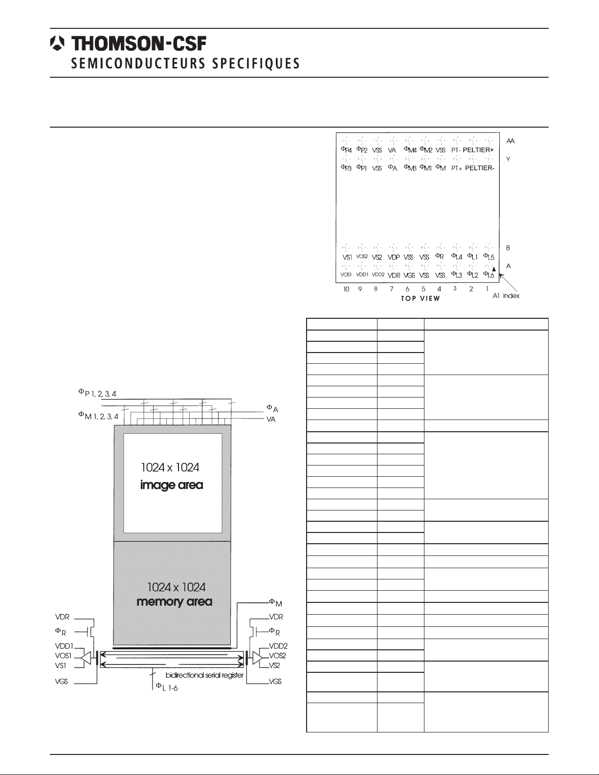
Figure 1 : TH7888A organization
TH7888A
PIN IDENTIFICATION
Pin N° Symbol Designation
Y9 FP1
AA9 FP2
Y10 FP3
AA10 FP4
Y5 FM1
AA5 FM2
Y6 FM3
AA6 FM4
Y4 FM
B2 FL1
A2 FL2
A3 FL3
B3 FL4
B1 FL5
A1 FL6
A9 VDD1
A8 VDD2
B10 VS1
B8 VS2
B7 VDP
A6 VGS
A10 VOS1
B9 VOS2
B4 FR
Y7 FA
A7 VDR
AA7 VA
A4, A5, B5, B6 VSS
Y8, AA4, AA8 VSS
AA1, AA2 PELTIER+
Y1, Y2 PELTIER -
Y3 PT+
AA3 PT-
Image zone clocks
Memory zone clocks
Memory to register clock
Readout register clocks
Output amplifier drain supply
Output amplifier source
supply
Protection drain bias
Register output gate bias
Video outputs
Reset clock
Antiblooming gate clock
Reset bias
Antiblooming diode bias
Substrate bias
OPTIONAL
Peltier cooler power supply
NC otherwise
OPTIONAL
Temperature sensor
Pt 100W DIN43760
NC otherwise
November 1999 1/16
Page 2

TH7888A
DESCRIPTION
TH7888A is especially designed for high data rate applications (up to 30 pict /s in 1024x1024 format progressive scan) in
medical and industrial fields.
This area array image sensor consists of a 1024 x 1024 pixels (14 mmx14mm) image zone associated to a memory zone
(masked with optical shield).
In order to increase data rate, it is provided 2 separate outputs that can be used for parallel readout. (readout frequency up
to 20 MHz / output leading to a total readout frequency of 40 MHz). These two outputs allow 3 readout modes (single or
dual port readout).
TH7888A is designed with antiblooming structure providing electronic shutter capability.
Moreover the2x2binning mode is available on this sensor. In that case, the image size is 512 x 512 with 28 mmx28mm
pixels.
TH7888A package is sealed with a specific anti-reflective window optimized in 400-700 nm spectrum bandwidth.
OPTIONS : the device can be delivered with integrated low power Peltier cooler in order to improve sensor performances in
high temperature environments (typically + 50°C).
FUNCTIONAL DIAGRAM
Figure 1 gives the general sensor organization.
Extra dark lines are provided for use as dark references or for smearing digital correction.
Extra dark pixels are provided for line dark reference clamping.
Each frame is made of 1056 video lines :
1 dummy line
n
12 useful dark reference lines (with optical shield)
n
3 isolation lines
n
1024 useful lines
n
n 3 isolation lines
n 12 dark reference lines (with optical shield)
n 1 dummy line
Each video line is made of 546 or 1058 elements, depending on readout mode (single or dual port modes):
n
12 inactive prescan elements
n
1 isolation element
n
16 useful dark references (with optical shield)
n
5 isolation elements
n
512 or 1024 useful video pixels
2/16
Page 3
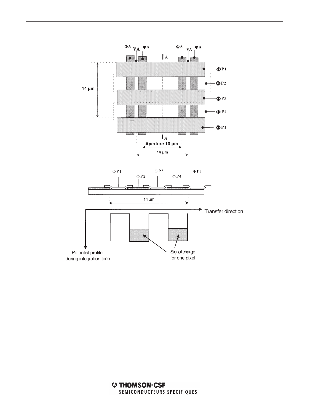
GEOMETRICAL CHARACTERISTICS
TH7888A
Figure 2b : Pixel layout
Figure 2c : Cross-section AA’
ABSOLUTE MAXIMUM RATINGS
Storage temperature ............................................................................................................................................-55°C to +150°C
Operating temperature...........................................................................................................................................-40°C to +85°C
Thermal cycling...............................................................................................................................................................15°C / mn
Maximum applied voltages :
Y9, AA9, Y10, AA10, Y5, AA5, Y6, AA6, Y4, B2, A2, A3, B3, B1, A1, B4, A6.................................................-0.3 to 15 V
A9, A8, B10, B8, B7, A7, AA7...........................................................................................................................-0.3 V to 15.5 V
Y7..............................................................................................................................................................................-0.3Vto12V
A4, A5, B5, B6, Y8, AA4, AA8 ..................................................................................................................................0V (ground)
3/16
Page 4
TH7888A
PELTIER OPTION
Storage temperature ..............................................................................................................................................-55°C to +85°C
Operating temperature...........................................................................................................................................-40°C to +70°C
Thermal cycling...............................................................................................................................................................10°C / mn
Maximum applied voltages :
PIN MAX VOLTAGE RANGE MAX CURRENT RANGE
AA1, AA2 with respect to Y1, Y2 5 V 1.8 A
Stresses above those listed under absolute maximum ratings may cause permanent device failure. Functionality at or above these limits is not implied. Exposure to absolute maximum ratings for extended periods may affect device reliability.
Operating range defines the limits whithin which the functionality is guaranteed.
Electrical limits of applied signals are given in operating conditions section
OPERATING PRECAUTIONS
Shorting the video outputs to any other pin, even temporarily, can permanently damage the on-chip output amplifier.
OPERATING CONDITIONS
TABLE1-DC CHARACTERISTICS
PARAMETER SYMBOL VALUE UNIT
Min. Typ. Max.
Output amplifier drain supply VDD1, VDD2 14.5 15 15.5 V
Protection drain bias VDP 14.5 15 15.5 V
Reset bias VDR 14.5 15 15.5 V
Antiblooming diode bias VA 14.5 15 15.5 V
Register output gate bias VGS 2.2 2.5 2.8 V
Output amplifier source supply VS1,2 0 V
Ground * VSS 0 V
OPTIONAL
Peltier power supply ** I
Voltage accross Peltier V
* Ground : note that the package metal back is internally grounded.
** Peltier power supply : conditions for 10°C sensor temperature with 50°C external temperature.
PELTIER
PELTIER
1.1 A
3V
4/16
Page 5
TH7888A
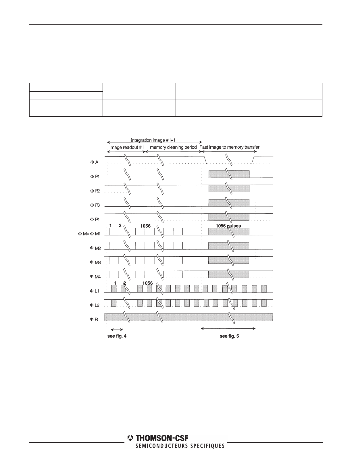
TIMING DIAGRAMS
Readout Mode
The serial readout register is operated in a two phase transfer mode. However, there are provided 6 separated command
electrodes that shall be connected differently depending on the required readout mode. The following table gives the connections to be made for each mode:
Readout modes Ü 1 output, VOS1 1 output, VOS2 2 outputs (parallel)
Drive clocks (signals) Þ (mirror effect)
FL1 pins B2, B3, B1 pins B2, A3, A1 pins B2, B3, A1
FL2 pins A2, A3, A1 pins A2, B3, B1 pins A2, A3, B1
The following diagrams are given for 20 MHz readout frequency, 1.25 MHz vertical transfer frequency
Figure 3 : Frame timing diagram
5/16
Page 6

TH7888A
1 : 12 Inactive pre-scan elements
2 : 1 isolation element
2:16 dark ref pixels
2:5 isolation elements
3 : 1024 useful video pixels (single output
3:readout mode)
2:512 useful video pixels (dual output
3:readout mode)
Figure 4 : Line timing diagram
6/16
Figure 5 : Vertical transfer during Image to memory zone transfer
Page 7

TH7888A
Figure 6 : Transfer period from image zone to memory zone (FP and FM) for 1.25 MHz vertical transfer frequency (Fv=1/Tv).
t1 = 7 ns typ. t2 = 5 ns typ. td = 8 ns typical delay time
Figure 7 : Output diagram for readout register and reset clock 20 MHz applications. Cross over of complementary clocks (F L1, F L2)
Figure 7 : between 30% and 70 % of max. amplitude.
7/16
Page 8

TH7888A
BINNING MODE OPERATION
In this mode, the image is composed of 512 x 512 pixels (28 mmx28mm each).
Fall times & rise times : see fig. 6& 7
Figure 8 : Summation in the readout register of 2 adjacent lines.
Figure 9 : Summation of 2 adjacent pixels
In binning mode operation, maximum level of elementary pixel (14 x 14 mm) is reduced to Vsat / 4.
8/16
Page 9

TH7888A
EXPOSURE TIME REDUCTION
TH7888A allows exposure time control (electronic shutter function).
The exposure time reduction is achieved by pulsing all the FPi gates to 0 volt so as to remove continuously all the photoge-
nerated electrons through antiblooming drain VA.
Fall times & rise times : see fig.5&6
Figure 10 : Timing diagram for electronic shutter
TABLE 2 - DRIVE CLOCK CHARACTERISTICS
Parameter Symbol Value Unit Remarks
Image zone clocks FP1,2, 3,4
High level 7.5 8 8.5 V
Low level 0 0.5 0.8 V
Memory zone clocks FM1,2,3,4
High level 7.5 8 8.5 V
Low level 0 0.5 0.8 V
Memory to register clocks FM
High level 8.5 9 9.5 V
Low level 0 0.5 0.8 V
Antiblooming gate FA
High level (integration) 3 4 7 V
Low level (transfer) 0 0.5 0.8 V
Reset gate FR
High level 10 12 13 V
Low level 0 2 3 V
Readout register clocks FL1,2
Min Typ Max
Typical input capacitance
15 nF
See figure 11
Typical input capacitance
15.5 nF
See figure 11
Typical input capacitance
10 pF
Typical input capacitance
14 nF
See figures 11 & 13
Typical input capacitance
10 pF
High level 8.5 9 9.5 V
Low level 0 0.5 0.8 V
Maximum readout register frequency F
Image zone to memory zone transfer
frequency
H
F
V
20 23 MHz See figure 7
1.25 1.7 MHz See figure 12
9/16
Page 10

TH7888A
Figure 11 : Drive clocks capacitance network
TABLE 3 - STATIC AND DYNAMIC ELECTRICAL CHARACTERISTICS
PARAMETER SYMBOL VALUE UNIT REMARKS
Min. TYP. Max.
Output amplifier supply current I
Output impedance Z
DC output level V
Output conversion factor CVF 5.5 6 6.5 µV/ e-
DD
s
REF
200 225 250 W
10 mA per amplifier
11 V
10/16
Page 11

TH7888A
ELECTROOPTICAL PERFORMANCE
• General conditions :
Temp = 25°C (package back temperature)
Light source : 2854K with 2 mm BG38 filter (unless specified) + F/3.5 optical aperture .
30 images per second mode (unless specified)
Typical operating conditions.
• Readout mode : 2 outputs
• Values exclude dummy elements and blemishes.
PARAMETER SYMBOL VALUE UNIT REMARKS
Min. TYP. Max.
Output register saturation level V
Pixel saturation level V
Pixel saturation charge (electron per pixel) Q
Responsivity at 640 nm
Responsivity with BG38 filter
Quantum efficiency at 640 nm QE 15 % see fig.15
Photo response non uniformity (1s) PRNU 1.3 1.7 % VOS
Dark signal non uniformity (1s) DSNU 0.28 0.4 mV Note 2
Average dark signal V
Temporal RMS noise in darkness (Last line) V
Dynamic range D 80 dB Note 6
Horizontal modulation transfer function at 500 nm MTF 70 % Note 7
Vertical charge transfer inefficiency VCTI 2.10
Horizontal charge transfer inefficiency HCTI 7.10
Note 1 : Pixel saturation (full well) as a function of vertical transfer frequency (see figure 12) and antiblooming
Note 1 : adjustment (see figure13).
Note 2 : After subtraction of dark signal slope due to memory readout time
Note 3 : First line level referenced from inactive prescan elements (12 samples)
Note 4 : Last line level referenced from inactive prescan elements (12 samples)
Note 5 : Measured with Correlated Double Sampling (CDS) including 160 µV readout noise and dark current noise
Note 5 : in the general test conditions.
Note 6 : Saturation to RMS noise in darkness ratio.
Note 7 : At Nyquist frequency.
Note 8 : VSAT / 2 measurement and 1.25 MHz vertical transfer frequency.
Note 9 : VSAT / 2 measurement and 20 MHz horizontal transfer frequency.
reg 2.3 2.6 V
SAT
SAT
SAT
R
DS
N
1.6 1.9 2.2 V Note 1
270 320 370 ke-
6.5
11
2 3 mV Note 3
4 5.6 mV Note 4
200 µV Note 5
-5
-5
V/µJ/cm²
mV/lux
Note 8
Note 9
11/16
Page 12

TH7888A
Figure 12 : Saturation level by full well with antiblooming out (FAhigh = 0 volt) vs the vertical transfer frequency.
N
with E
conditions)
= number of times E
ESAT
SAT=VSAT
12/16
Figure 13 : Saturation level limitation by the antiblooming effect on the pixel (Typical operating conditions)
SAT
/ Responsivity (typical illumination
Figure 14 : Smearing effect
V
SMEARING
V
=××
SAT
N
TI= integration time
TV= image to memory transfer time
ESAT
T
V
T
I
H
Page 13

IMAGE QUALITY GRADE
Blemish
Max area of2x2 defective pixels
TH7888A
Quantum Efficiency
Figure 15 : Spectral response.
Clusters
Less than 7 contiguous defects in a column
Columns
More than 7 contiguous defects in a column
General conditions
Room temperature..................................................................................................................................................................25°C
Frequency.....................................................................................................................................................................30 images/s
.............................................................................................................................................................typical operating conditions
Considered image zone .............................................................................................................................................1024 x 1024
Light source ....................................................................................................2854 K with BG38 filter + F/3.5 optical aperture
At Vos =0.7 Vsat.
TYPE WHITE BLACK
Blemishes / clusters a >20%Vos
Columns a >10%Vos êaï 10 % Vos
In darkness
Blemishes / clusters a>10 mV (*)
Columns a >5mV(*)
(*) reference is Vo : average darkness signal
Number of defects
Total pixel number affected by blemishes and clusters:.......................................................................................................100
Maximum number of clusters:.....................................................................................................................................................10
Maximum number of columns:......................................................................................................................................................5
a : amplitude of video signal of defect with respect to mean output voltage Vos
êaï 30 % Vos
Ordering code :
TH7888AVRHRB
TH7888ACBHRB (OPTIONAL: with integrated Peltier cooler)
13/16
Page 14

TH7888A
PACKAGE OUTLINE DRAWING (standard)
*
Legend
All values are in mm.
1 : black alumina 40 pins PGA package
2 : black optical mask
3 : 400nm - 700 nm AR coated window (R<1 % per side)
4 : Metal back, (CuW - copper tungsten) gold plated. Electrically grounded (VSS).
5 : Optical center.
6 : first useful pixel (readout through V
7 : mechanical reference
OS1
)
*
*
Ø3.04 ±0.04
0.5
14/16
Z
top
Z
bottom
Mechanical
distance
±0.31 2.31 ±0.29
2.82
1.68 ±0.15 2.19 ±0.17
Optical
distance
Page 15

PACKAGE OUTLINE DRAWING (Peltier option)
TH7888A
*
Legend
All values are in mm.
1 : black alumina 40 pins PGA package
2 : black optical mask
3 : 400nm - 700 nm AR coated window (R<1 % per side)
4 : Metal part with integrated Peltier element.
5 : Metal back, (CuW - copper tungsten) gold plated. Electrically grounded (VSS).
6 : Optical center.
7 : first useful pixel (readout through V
8 : mechanical reference
OS1
)
*
*
Ø3H8
0.5
Z
top
Z
bottom
Mechanical
distance
2.98
±0.68 2.48 ±0.58
4.50 ±0.32 5.00 ±0.33
Optical
distance
15/16
Page 16

TH7888A
Information furnished is believed to be accurate and reliable. However THOMSON-CSF SEMICONDUCTEURS SPECIFIQUES
assumes no responsability for the consequences of use of such information nor for any infringement of patents or other rights of
third parties which may result from its use. No license is granted by implication or otherwise under any patent or patent
rights of THOMSON-CSF SEMICONDUCTEURS SPECIFIQUES. Specifications mentioned in this publication are subject to
change without notice. This publication supersedes and replaces all information previously supplied. THOMSON-CSF
SEMICONDUCTEURS SPECIFIQUES products are not authorized for use as critical components in life support devices
or systems without express written approval from THOMSON-CSF SEMICONDUCTEURS SPECIFIQUES. 1999 THOMSONCSF SEMICONDUCTEURS SPECIFIQUES - Printed in France - All rights reserved.
This product is manufactured by THOMSON-CSF SEMICONDUCTEURS SPECIFIQUES - 38521 SAINT-EGREVE / FRANCE.
For further information please contact : THOMSON-CSF SEMICONDUCTEURS SPECIFIQUES - Route Départementale
128 - B.P. 46 - 91401 ORSAY Cedex / FRANCE - Tél. : (33)(0) 1.69.33.03.24 / Téléfax : (33)(0) 1.69.33.03.21.
E-mail : monique.lafrique@tcs.thomson-csf.com - Internet : http://www.tcs.thomson-csf.com
16/16
ORDER CODE : DSTH7888AT/1199 Créé / réalisé par Graphic Express - Tél. : 01.46.55.27.24 - 10688 - 11/99
 Loading...