

Page 1

Features
• 1024 x 1024 Pixels with Memory Zone
• Up to 60 Images/Second
• Built-in Antiblooming Device Providing an Electronic Shutter Function
• Pixel: 14 µmx14µm
• Image Zone: 14.34 x 14.34 mm²
• Four Outputs (256 x 1024 pixels) at 20 MHz Each
• Possible Binning 2 x 2
• Optical Shield against Parasitic Reflexions and Stray Light
• A/R Window in 400 - 700 nm Bandwidth
Description
The TH7887A is especially designed for high data rate applications (up to 60 pict/s) in
medical and industrial fields.
This area array image sensor consists of a 1024 x 1024 pixels (14
zone associated to a memory zone (masked with optical shield).
In order to increase data rate, the image zone is divided into four zones (256 x 1024
each) which are read in parallel through 4 different outputs (readout frequency up to
20 MHz/output leading to a total readout frequency of 80 MHz).
The TH7887A is designed with antiblooming gates.
Moreover, the 2 x 2 binning mode is available on this sensor. In this case, the image
size is 512 x 512 with 28
The TH7887A is sealed with a specific anti-reflective window optimized in 400 700 nm bandwidth.
µmx28µm pixels. Each output will read 128 x 512 pixels.
µmx14µm) image
Area Array CCD
Image Sensor
1024 x 1024
Pixels with
Antiblooming
TH7887A
Rev. 2146A–IMAGE–05/02
1
Page 2
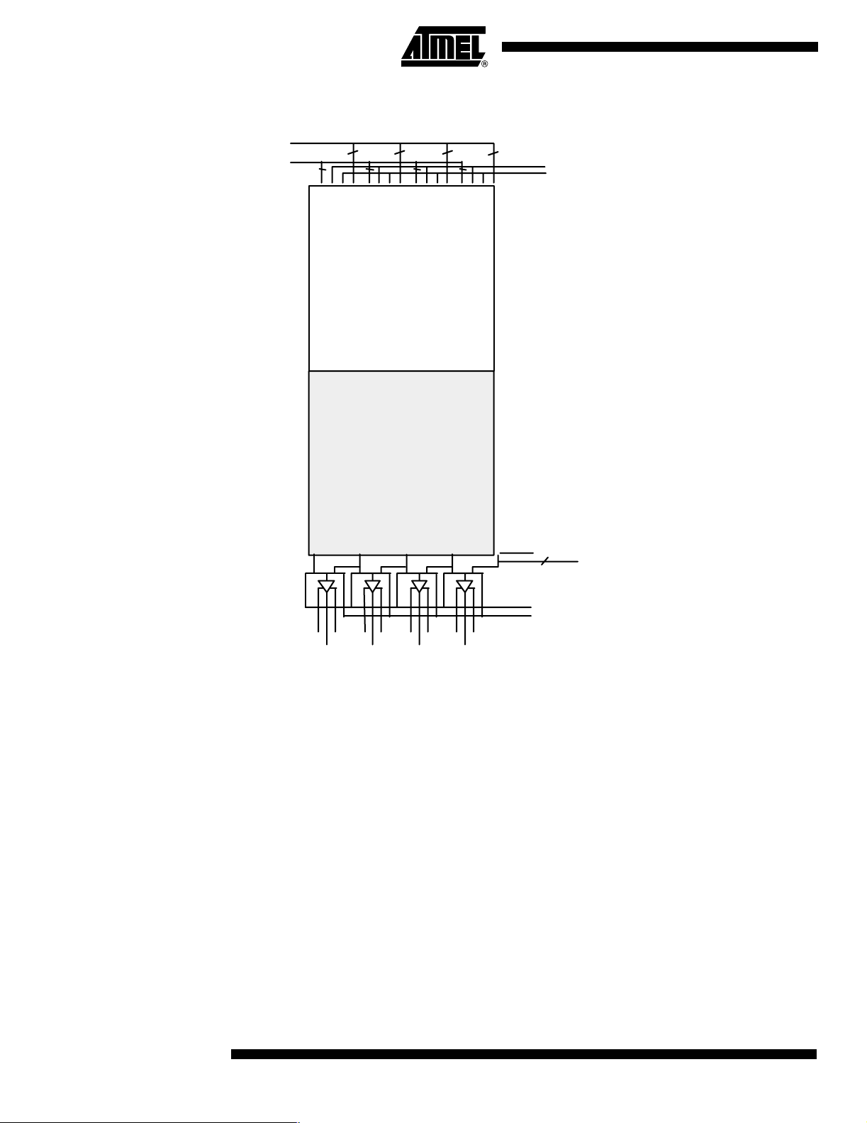
Figure 1. TH7887A Organization
1, 2, 3, 4
PΦ
1, 2, 3, 4
M
Φ
A
Φ
VA
1024 x 1024
Image Zone
1024 x 1024
Memory Zone
VDD1 VS1 VDD2 VS2
VOS1 VOS2 VOS3 VOS4
VDD3 VS3
VDD4 VS4
Φ
M
VGS
ΦR
L 1,2Φ
2
TH7887A
2146A–IMAGE–05/02
Page 3
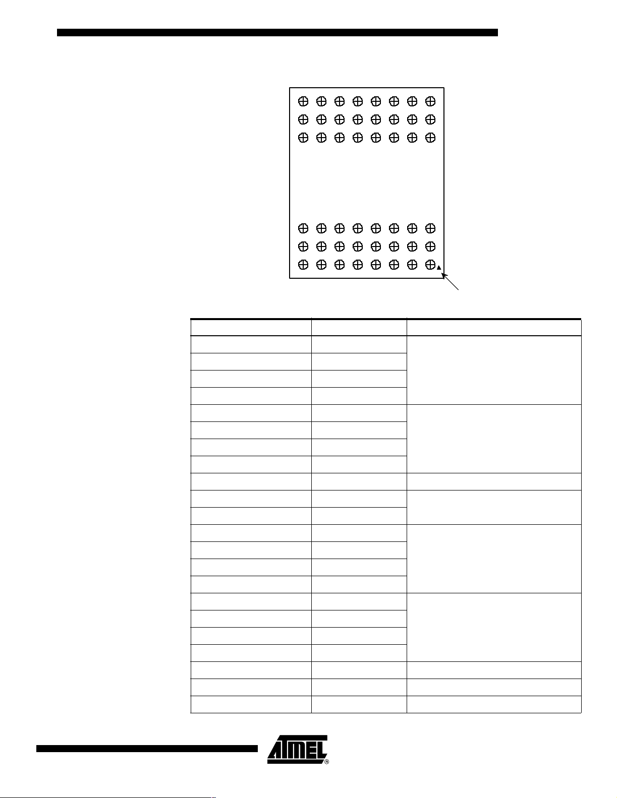
Pin Identification
TH7887A
VA
AA
W
V
C
B
A
VSS VOS2 VOS1VOS3VOS4 R
Φ
L1 VSS VDR VS4 VS3 VS2 VS1 VSSΦ
L2 M VGS VDD4 VDD3 VDD2 VDD1 VSSΦ Φ
A M4 M3 ΦP3 P2
VSS M2
VSS M1 P4 P1 M4 M1 ΦP4 VSSΦΦΦΦΦ
VDDP N.C
ΦM2
ΦΦΦΦ
VSS P2 M3 VSS P3 VSS
87654321
ΦP1
ΦΦΦΦ
TOP VIEW
Pin Number Symbol Designation
A2, A6
B2, C5
B5, C3
A5, C2
A3, A7
B7, C4
B4, C6
C7, A4
(1)
(1)
(1)
(1)
(1)
(1)
(1)
(1)
ΦP4
ΦP3
Image zone clocks
ΦP2
ΦP1
ΦM1
ΦM2
Memory zone clocks
ΦM3
ΦM4
A1
Index
2146A–IMAGE–05/02
V7 ΦM Memory to register clock
W8 ΦL1
Readout register clocks
V8 ΦL2
V2 VDD1
V3 VDD2
Output amplifier drain supply
V4 VDD3
V5 VDD4
W2 VS1
W3 VS2
Output amplifier source supply
W4 VS3
W5 VS4
AA6 VDDP Screen voltage
AA5 NC Not connected
V6 VGS Register output gate bias
3
Page 4

Pin Number Symbol Designation
AA1 VOS1
AA2 VOS2
AA3 VOS3
AA4 VOS4
AA8 ΦR Reset clock
C8 ΦA Antiblooming gate clock
W6 VDR Reset bias
C1 VA Antiblooming diode bias
AA7, V1, W1 VSS
B6, B1, A1, B3 VSS
Note: 1. Short circuited on package.
Video output signal
Substrate biasW7, A8, B8 VSS
4
TH7887A
2146A–IMAGE–05/02
Page 5
TH7887A
e
Geometrical Characteristics
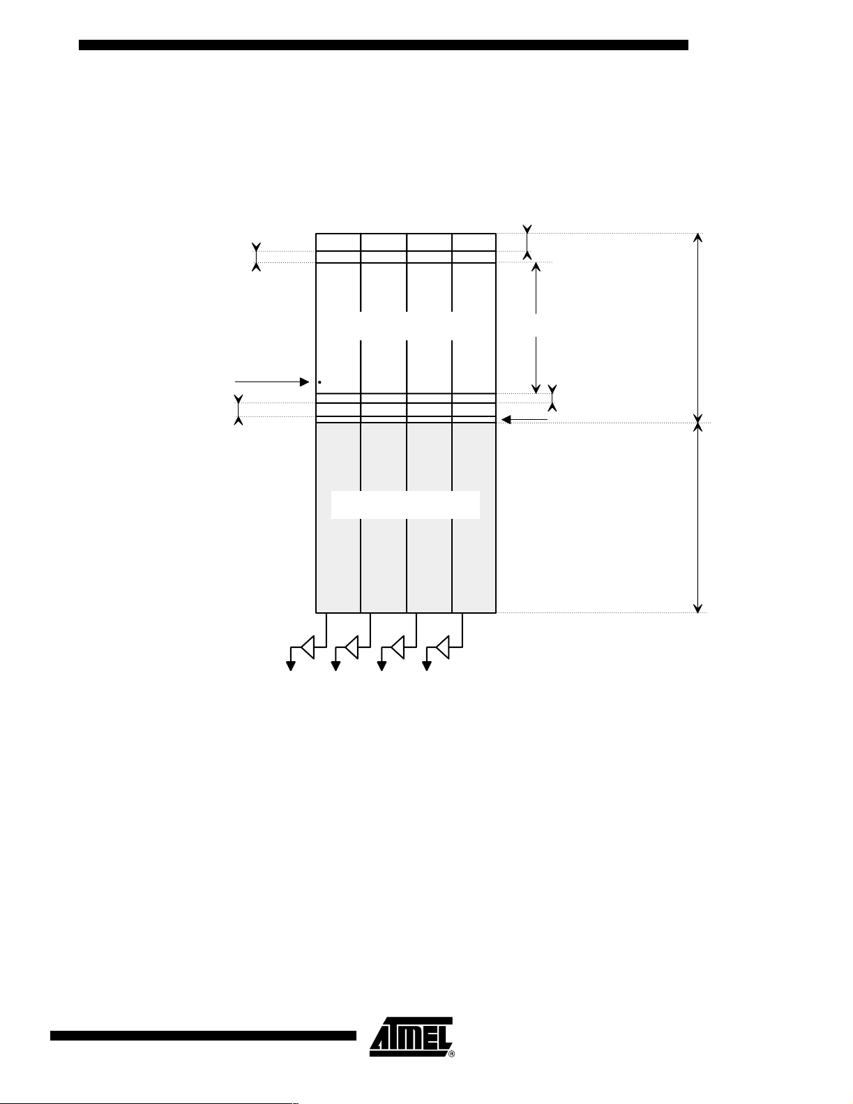
Figure 2. Video Line (on each output)
3 isolation lines
First pixel
6 dark reference lines
The image zone features 1024 useful lines (+ 20 extra lines) of 1024 pixels. For readout
only, the full frame is split into 4 blocks of 256 columns.
The video line consists of 256 useful pixels, and 273 elements in total (for each output).
Image zone
Memory zone
7 dark reference lines
1024 useful pixels
3 isolation lines
1 inactive line
1044 line
1044 lin
Pixels 1 to 17 : inactive prescan elements
Pixels 18 to 273 : useful elements
2146A–IMAGE–05/02
Vos1 Vos2 Vos3 Vos4
5
Page 6
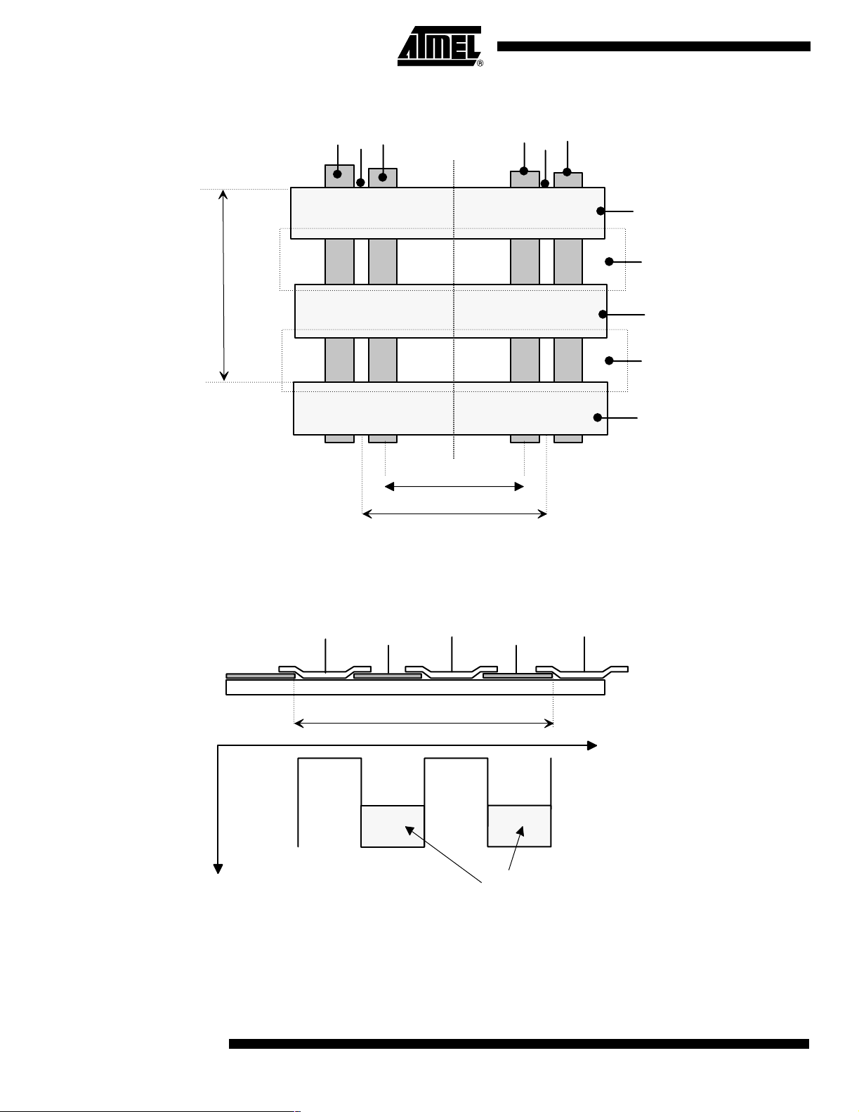
Figure 3. Pixel Layout
14 µm
Φ A Φ A Φ A Φ A
VA
VA
A
A'
Aperture 10.3 µm
14 µm
Φ P1
Φ P2
Φ P3
Φ P4
Φ P1
Figure 4. Cross-section AA’
Potential profile
during integration time
Φ P1
Φ P2
14 µm
Φ P3
Φ P4
Signal charge
for one pixel
Φ P1
Transfer direction
6
TH7887A
2146A–IMAGE–05/02
Page 7

Absolute Maximum Ratings*
Storage Temperature .................................... -55°Cto+150°C
Operating Temperature ............................... -40°Cto+85°C
Thermal Cycling.........................................................15°C/mm
Maximum Applied Voltages:
A2, A6, B2, C5, B5, C3, A5, C2, A3, A7, B7, C4
B4, C6, C7, A4, V7, W8, V8, AA8, V6, AA5..........-0.3V to 15V
V2,V3,V4,V5,W2,W3,W4,W5
W6, C1, AA6 ...................................................... -0.3V to 15.5V
C8 .........................................................................-0.3V to 12V
AA7, V1, W1, W7, A8, B8, B6, B1, A1, B3 ............. Ground 0V
TH7887A
*NOTICE: Stresses above those listed under absolute max-
imum ratings may cause permanent device failure. Functionality at or above these limits is not
implied. Exposure to absolute maximum ratings
for extended periods may affect device reliability.
Operating Range
The operating range defines the limits where function is guaranteed.
Electrical limits of applied signals are given in the operating conditions section.
Operating Precautions
Shorting the video outputs to any other pin, even temporarily, can permanently damage
the on-chip output amplifier.
Operating Conditions
Table 1 . DC Characteristics
Value
Parameter Symbol
Output amplifier drain supply
Screen voltage VDDP 14.5 15 15.5 V
Reset bias VDR 14.5 15 15.5 V
Antiblooming diode bias VA 14.5 15 15.5 V
Register output gate bias VGS 2.2 2.5 2.8 V
VDD1, VDD2,
VDD3, VDD4
14.5 15 15.5 V
UnitMin Typ Max
Output amplifier source supply VS1,2,3,4 – 0 – V
Ground VSS – 0 – V
2146A–IMAGE–05/02
7
Page 8

Timing Diagram The following diagrams are given for:
• 20 MHz readout frequency
• 1.25 MHz vertical transfer frequency
Readout of one image is performed in 2 steps:
• image zone to memory zone transfer
• memory zone to register transfer and readout of register
This last step is also an integration period, the duration of which can also be increased
according to the required frame rates.
Figure 5. Frame Timing Diagram
Integration period
Φ A
P1
Φ
Φ P2
Φ P3
Picture readout
Cleaning period (*)
Image to memory zone
Transfer
Memory zone
Φ P4
Φ M1
Φ M2
Φ M3
Φ M4
Φ L1
Φ L2
Φ R
=Φ M
15
15
See fig. 6
1044
1044
1044 pulses
See fig. 7
(*) During the cleaning period, memory clocks must be pulsed as during readout time
(specially for high temperature applications).
8
TH7887A
2146A–IMAGE–05/02
Page 9
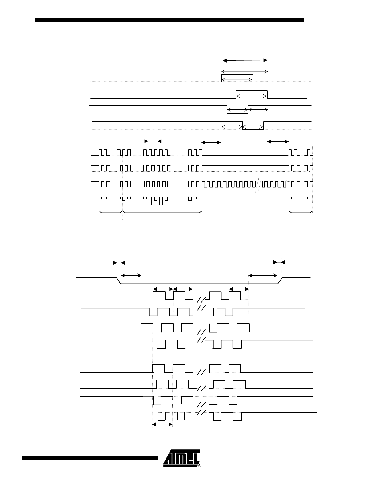
Figure 6. Line Timing Diagram
Φ M1
=
Φ M
TH7887A
Item fig.8
7To
5To
Φ M2
Φ M3
Φ M4
See fig. 9
Φ L1
Φ L2
Φ R
Vos 1,2,3,4
1 17 18 273 min
1
2
1 : 17 inactive pre-scan elements
2 : 256 useful video pixels
Figure 7. Vertical Transfer During Image to Memory Zone Transfer
20 ns < tf < 2 To
100 ns min.
Φ A
1
Φ P1
2
100 ns min.
3To
3To
1044
5To
3To
3To
100 ns min.
100 ns min.
20 ns < tr < 2 To
17
1
1
Φ M1
2146A–IMAGE–05/02
Φ P2
Φ P3
Φ P4
=
Φ M2
Φ M3
Φ M4
Φ M
See fig. 8
9
Page 10

Figure 8. Transfer Period from Image Zone to Memory Zone (ΦPandΦM)
for 1.25 MHz Vertical Transfer Frequency (Fv = 1/Tv)
Tv=800 ns
Φ M2
Φ M3
Φ M4
tr
To = Tv / 8
3 To
tf
5 To
5 To
3 To 5 To
3 To
Φ P1
Φ P2
Φ P3
Φ P4
=Φ M1
=
=
=
Figure 9. Output Diagram for Readout Register and Reset Clock 20 MHz Applications
50 ns
16 ns min
Φ
L1
16 ns min
25 ns < tr < To/3
25 ns < tf < To/3
To = 100 ns
t1
12 ns min
t2 t2
td
Reset feedthrough
td = 8 ns typical delay time
A
0.3A
td
Φ
L2
Φ
R
Vos 1,2,3,4
t1
Signal
level
t1 = 10 ns typ.
t2 = 5 ns typ.
Cross over of complementary clocks (Φ L1, Φ L2) between 30% and 70% of maximum amplitude.
10
TH7887A
2146A–IMAGE–05/02
Page 11

TH7887A
Binning Mode
In this mode, the image is composed of 512 x 512 pixels (28 µmx28µm each).
Operation
Figure 10. Summation in the Readout Register of 2 Adjacent Lines.
15 To
5To 3To 5To
Φ M1
5To 3To 5To
Φ M2
Φ M3
Φ M1
Φ M
=Φ M1
100 ns min
3To
3To 5To 3To
5To 3To
3T0
Fall times and rise times:
see figures 8 & 9
3To
100 ns min
Φ L1
Φ L2
Figure 11. Summation of 2 Adjacent Pixels
Φ L1
Φ L2
Φ R
Vos 1,2,3,4
Output reset frequency
divided by 2
Pixel i
Useful signal
Pixel i
+
Pixel i+1
In binning mode operation maximum level of elementary pixel (14 x 14 µm) is reduced to Vsat/4.
2146A–IMAGE–05/02
11
Page 12

Exposure Time
The TH7887A allows exposure time control (electronic shutter function).
Reduction
The exposure time reduction is achieved by pulsing all the Φ Pi gates to 0V to continuously remove all photogenerated electrons through antiblooming drain VA.
Figure 12. Timing Diagram for Electronic Shutter
Image period
Φ
A
Φ
Φ
Φ
Φ
1 µs
P1
P2
P3
P4
1 µs
Table 2 . Drive Clock Characteristics
Parameter Symbol
Image zone clocks
High level
Low level
Memory zone clocks
High level
Low level
Memory to register clocks
High level
Low level
Antiblooming gate
High level (integration)
Low level (transfer)
ΦP1,2,3,4
ΦM1,2,3,4
ΦM
ΦA
Transfer
Fall times and rise times: see figures 7 & 8
Value
8.5
0
8.5
0
8.5
0
5.5
0
9
0.5
9
0.5
9
0.5
5.5
0.5
Obturation
9.5
0.8
9.5
0.8
9.5
0.8
5.5
0.8
Unit RemarksMin Typ Max
V
V
V
V
V
V
V
V
Integration
Typical input capacitance
15 nF
See Figure 13
Typical input capacitance
15.5 nF
See Figure 13
Typical input capacitance
10 nF
Typical input capacitance
14 nF
See Figure 13 and Figure 15
12
TH7887A
2146A–IMAGE–05/02
Page 13

Table 2 . Drive Clock Characteristics (Continued)
TH7887A
Value
Parameter Symbol
Reset gate
High level
Low level
Readout register clocks
High level
Low level
Maximum readout register
frequency
Image zone to memory zone
transfer frequency
ΦR
ΦL1, 2
ΦF
H
ΦF
V
Figure 13. Capacitance Network for Drive Clocks
Φ P2
3.4 nF
2.5 nF
Φ P1
3.3 nF
ΦA
2.5 nF
Φ P3
1.4 nF
ΦP4
Unit RemarksMin Typ Max
Typical input capacitance
10
0
8.5
0
– 20 23 MHz See Figure 9
– 1.25 1.7 MHz See Figure 14
11
0.5
9
0.5
12
0.8
9.5
0.8
V
V
Φ L1 Φ L2
V
V
10 pF
50 pF
60 pF 75 pF
Φ P2
0.7 nF
0.5 nF
Φ P1
0.7 nF
VA
0.5 nF
ΦP3
1.3 nF
Φ A
Φ P4
2146A–IMAGE–05/02
3.2 nF 4.9 nF 2.2 nF
2.2 nF
Φ P1 Φ P2
4.4 nF
4.4 nF4.4 nF
3.4 nF
Φ P4 Φ P3
3.9 nF 4.4 nF 3.2 nF
3.2 nF
Φ M1 Φ M2
4.4 nF
4.4 nF4.4 nF
3.9 nF
Φ M4 Φ M3
13
Page 14

Electrical Performances
Table 3 . Static and Dynamic Electrical Characteritics
Value
Parameter Symbol
Output amplier supply current I
Output impedance Z
DC output level V
Output conversion factor CVF 7.8 8 8.2 µV/ e-
Electro-optical Performances
DD
S
REF
• General test conditions:
– To p = 2 5 °C (package back temperature).
– 8.5 – mA per amplifier
200 225 250 Ω
– 11.5 – V
Unit RemarksMin Typ Max
– Light source: 2854K with 2 mm BG38 filter (unless specified) + F/3.5 optical
aperture.
– 60 images per second mode (unless specified).
– Typical operating conditions.
• Readout on each output.
• Measurements exclude dummy elements and blemishes.
Table 4 . Electro-Optical Performance Characteristics
Value
Parameter Symbol
Saturation output level V
Responsivity at 640 nm
Responsivity with BG38 filter
Quantum efficiency at 640 nm QE – 14 – % See Figure 17
Gain dispersion between outputs ∆G – 12%
Photo response non-uniformity
(1σ)
Dark signal non-uniformity (1σ)DSNU – 0.14 0.2 mV
Average dark signal V
Temporal RMS noise in darkness
(Last line)
Dynamic range D – 80 – dB
SAT
R
PRNU – 1.3 1.7 % VOS
DS
V
N
1.6 2 2.4 V
7
–
–
–
– 200 – µV
12
8
1
2
–
–
1.5
2.8
Unit RemarksMin Typ Max
V/µJ/cm
mV/lux
mV
mV
(1)
2
(2)
(3)
(4)
(5)
(6)
14
TH7887A
2146A–IMAGE–05/02
Page 15

Table 4 . Electro-Optical Performance Characteristics (Continued)
Value
TH7887A
Parameter Symbol
Horizontal modulation transfer
function at 500 nm
Vertical charge transfer
inefficiency
Horizontal charge transfer
inefficiency
Notes: 1. Pixel saturation (full well) as a function of vertical transfer frequency (see Figure 14) and antiblooming adjustment (see Fig-
ure 15).
2. After subtraction of dark signal slope due to memory readout time.
3. First line level referenced from inactive prescan elements (17 samples).
4. Last line level referenced from inactive prescan elements(17 samples).
5. Measured with Correlated Double Sampling (CDS) including 160 µV readout noise and dark current noise in the general test
conditions.
6. Saturation to RMS noise in darkness ratio.
7. At Nyquist frequency.
8. VSAT/2 measurement and 1.25 MHz vertical transfer frequency.
9. VSAT/2 measurement and 20 MHz horizontal transfer frequency.
MTF – 70 – %
VCTI ––2.10
HCTI ––7.10
-5 (8)
-5 (9)
Unit RemarksMin Typ Max
(7)
Figure 14. Saturation Level by full well with antiblooming out (ΦAhigh=0V)
vs the Vertical Transfer Frequency
3.5
3
Readout stage limit
2.5
2
1.5
1
Saturation Output Level (Volts)
0.5
0
200
Vertical Transfer Frequency (KHz)
1200700 1700
2146A–IMAGE–05/02
15
Page 16
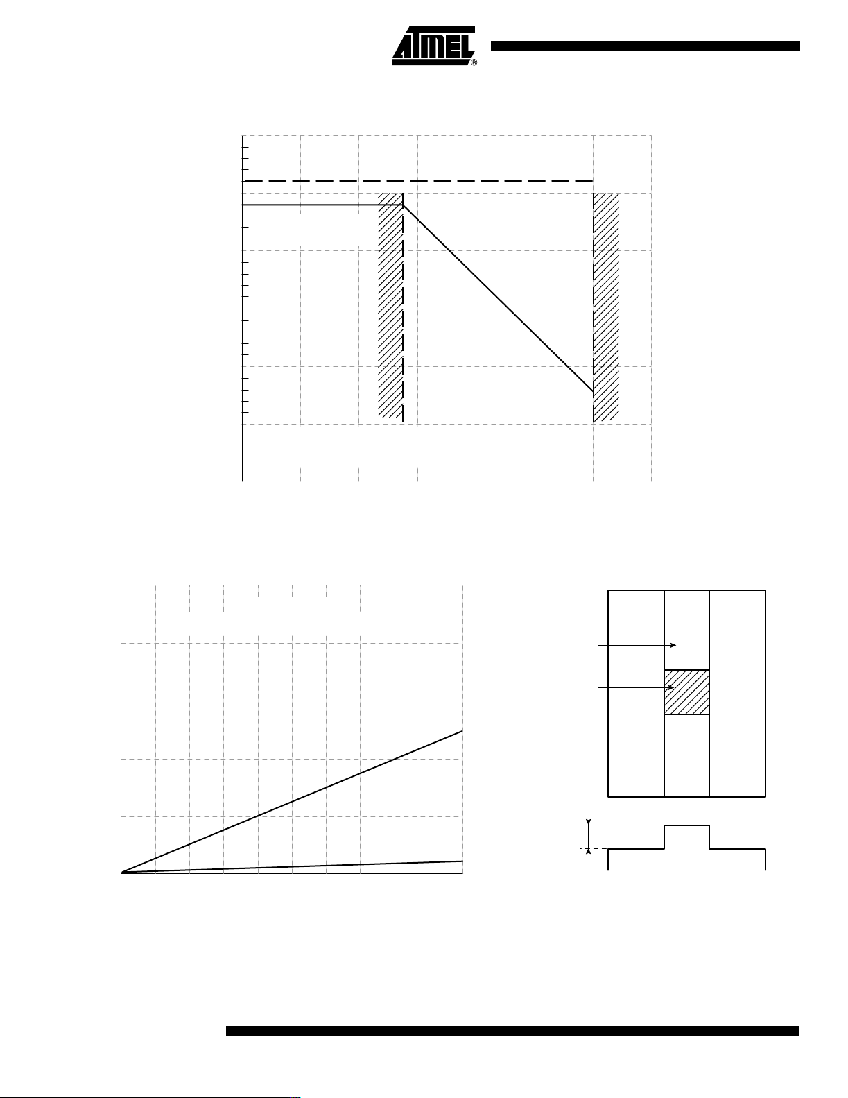
Figure 15. Saturation Level Limitation by the Antiblooming Effect on the Pixel
3
Readout stage limit
2.5
Saturation Output Level (Volts)
Figure 16. Smearing Effect
100
1.2 MHZ vertical tranfer frequency
80
Inefficient
2
1.5
1
0.5
0
23456
antiblooming
1.2 MHz
vertical transfer frequency
ΦA High Clock Level (Volts)
60 images / sec.
Efficient
antiblooming
789
Vertical smearing
60
40
Smearing/Vsat (%)
20
0
0123456
16
TH7887A
100xEsat
78910
Overilluminated Zone (% Image Height)
10xEsat
Overillumination
Smearing level
a
b
a,b signal line
2146A–IMAGE–05/02
Page 17

Figure 17. Spectral Response
20
15
10
Quantum efficiency (%)
5
0
400 450 500 550 600 650 700
TH7887A
750 800 850 900 950 1000 1050 1100
Lambda (mm)
Image Quality Grade
Blemish Max area of 2 x 2 defective pixels.
Clusters Less than 7 contiguous defects in a column.
Columns More than 7 contiguous defects in a column.
General Measurement Conditions
Room temperature 25°C
Frequency
Considered image zone 1024 x 1024
Light source 2854 K with BG38 filter + F/3.5 optical aperture
60 images/second
typical operating conditions
Table 5 . At VOS=0.7Vsat.
Type White Black
Blemishes/clusters α >20%Vos
Columns α > 10% Vos
Table 6 . In darkness, T = 25°C, 60 images/second
Blemishes/clusters α >10mV
Columns α >5mV
Note: 1. Reference is Vo : average darkness signal
S
êα ï> 30% Vos
êα ï
> 10% Vos
(1)
(1)
2146A–IMAGE–05/02
17
Page 18

Number of Defects
Total pixel number affected by blemishes and clusters 100
Maximum number of clusters 10
Maximum number of columns 5
α : amplitude of video signal of defect with respect to mean output voltage Vos
Ordering Code TH7887AVRH
18
TH7887A
2146A–IMAGE–05/02
Page 19
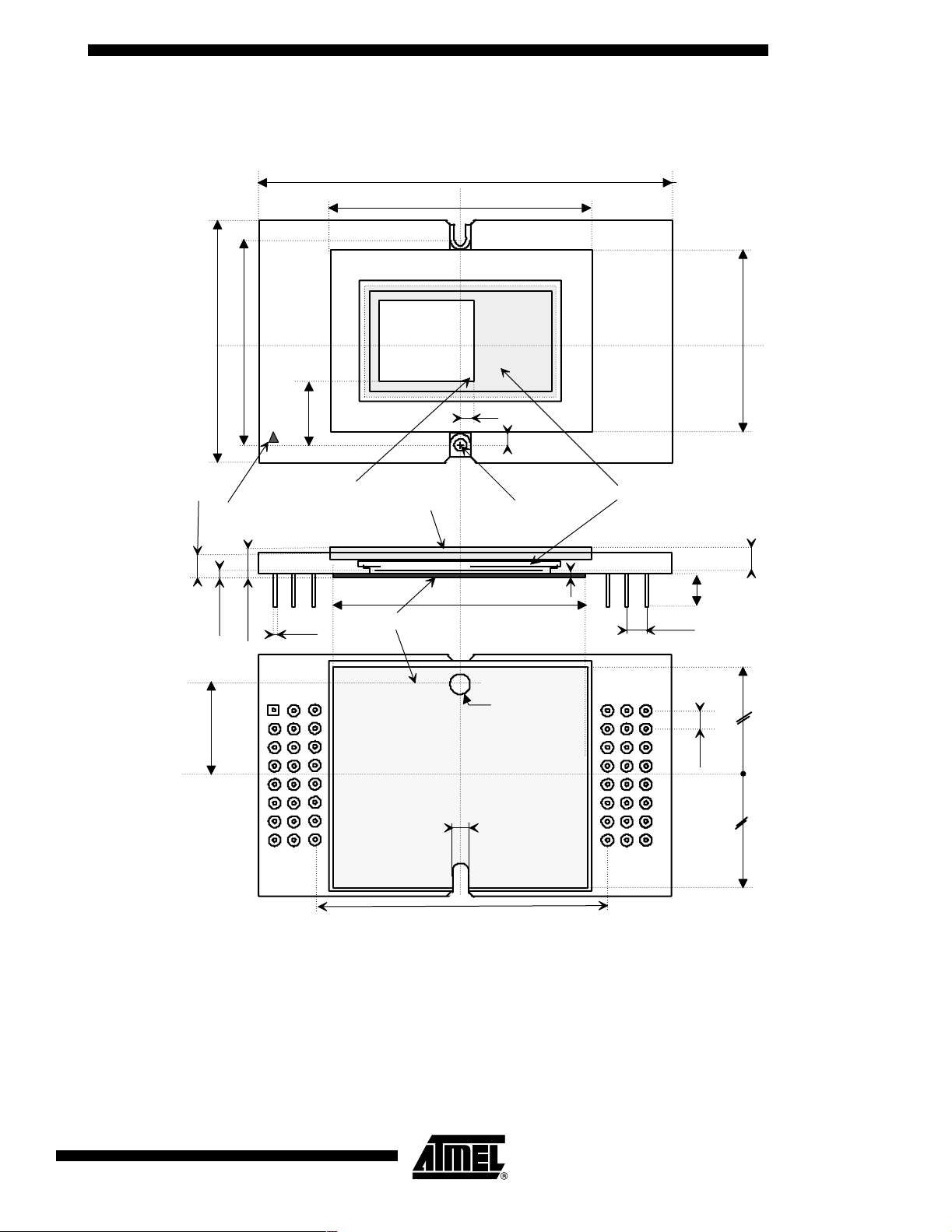
Outline Drawing
TH7887A
TOP VIEW
55.88
42.5
2.54± 0.25
33.5
1.06±0.1
1
2
3
14.25
4
5
6
7
8
28.5
3.64 ± 0.40
Φ
y
0.46
x = 0.45 ± 0.10
y = 7.17 ± 0.10
36.6
x
2.2 ± 0.04
Φ
2.2 ± 0.05
Φ
.75
1
0.51
25
4.6
2.54
2.54 typ
32.25
2146A–IMAGE–05/02
C
B
A
1st useful pixel - readout through Vos1
Photosensitive area
Glass window thickness: 1.5 ± 0.1 mm
(antireflective coating with
400 - 700 nm transmission: 99%)
A1 index
Optical shield
40.64
BOTTOM VIEW
Reference for first pixel position
Optical distance between photosensitive area and
- external face of the window: 1.93 ± 0.30 mm
- back side of the package: 1.71 ± 0.15 mm
Metal plate connected to VSS
Parallelism between CCD and back side has
a maximum value of 100 µm
AA
W
V
Tolerance unless specified
All values in mm
± 1%
19
Page 20

Atmel Headquarters Atmel Operations
Corporate Headquarters
2325 Orchard Parkway
San Jose, CA 95131
TEL 1(408) 441-0311
FAX 1(408) 487-2600
Europe
Atmel Sarl
Route des Arsenaux 41
Case Postale 80
CH-1705 Fribourg
Switzerland
TEL (41) 26-426-5555
FAX (41) 26-426-5500
Asia
Atmel Asia, Ltd.
Room 1219
Chinachem Golden Plaza
77 Mody Road Tsimhatsui
East Kowloon
Hong Kong
TEL (852) 2721-9778
FAX (852) 2722-1369
Japan
Atmel Japan K.K.
9F, Tonetsu Shinkawa Bldg.
1-24-8 Shinkawa
Chuo-ku, Tokyo 104-0033
Japan
TEL (81) 3-3523-3551
FAX (81) 3-3523-7581
Memory
Atmel Corporate
2325 Orchard Parkway
San Jose, CA 95131
TEL 1(408) 441-0311
FAX 1(408) 436-4314
Microcontrollers
Atmel Corporate
2325 Orchard Parkway
San Jose, CA 95131
TEL 1(408) 441-0311
FAX 1(408) 436-4314
Atmel Nantes
La Chantrerie
BP 70602
44306 Nantes Cedex 3, France
TEL (33) 2-40-18-18-18
FAX (33) 2-40-18-19-60
ASIC/ASSP/Smart Cards
Atmel Rousset
Zone Industrielle
13106 Rousset Cedex, France
TEL (33) 4-42-53-60-00
FAX (33) 4-42-53-60-01
Atmel Colorado Springs
1150 East Cheyenne Mtn. Blvd.
Colorado Springs, CO 80906
TEL 1(719) 576-3300
FAX 1(719) 540-1759
RF/Automotive
Atmel Heilbronn
Theresienstrasse 2
Postfach 3535
74025 Heilbronn, Germany
TEL (49) 71-31-67-0
FAX (49) 71-31-67-2340
Atmel Colorado Springs
1150 East Cheyenne Mtn. Blvd.
Colorado Springs, CO 80906
TEL 1(719) 576-3300
FAX 1(719) 540-1759
Biometrics/Imaging/Hi-Rel MPU/
High Speed Converters/RF Datacom
Atmel Grenoble
Avenue de Rochepleine
BP 123
38521 Saint-Egreve Cedex, France
TEL (33) 4-76-58-30-00
FAX (33) 4-76-58-34-80
Atmel Smart Card ICs
Scottish Enterprise Technology Park
Maxwell Building
East Kilbride G75 0QR, Scotland
TEL (44) 1355-803-000
FAX (44) 1355-242-743
e-mail
literature@atmel.com
Web Site
http://www.atmel.com
© Atmel Corporation 2002.
Atmel Corporation makes no warranty for the use of its products, other than those expressly contained in the Company’s standard warranty
whichisdetailedinAtmel’s Terms and Conditions located on the Company’s web site. The Company assumes no responsibilit y for any errors
which may appear in this document, reser ves the right to change devices or specifications detailed herein at any time without notice, and does
not make any commitment to update the information contained herein. No licenses to patents or other intellectual property of Atmel are granted
by the Company in connection with the sale of Atmel products, expressly or by implication. Atmel’s products are not authorized for use as critical
components in life support devices or systems.
AT ME L®is the trademarks of Atmel.
Other terms and product names may be the trademar ks of others.
Printed on recycled paper.
2146A–IMAGE–05/02 0M
 Loading...