

Page 1
Features
• 6.5 µm x 6.5 µm Photodiode Pixel, at 6.5 µm Pitch
• 2 x 2 Outputs
• High Output Data Rate: 4 x 5 MHz
• High Dynamic Range: 10000: 1
• Antiblooming and Exposure Time Control
• Very Low Lag
• 56 lead 0.6" DIL Package
Description
Atmel’s TH7834C is a linear sensor based on charge-coupled device (CCD) technology. It can be used in a wide range of applications thanks to operating mode flexibility,
very high definition and high dynamic range (document scanning, digital photography,
Art, Industrial and Scientific Applications).
Pixel 1
mark
VOS1
VDR1
VS1
ΦR1-2
VSS
VST
ΦA1-2
VGS1-2
VS
Φ3A
Φ1A
Φ4A
Φ2A
VSS
VSS
Φ2C
Φ4C
Φ1C
Φ3C
VSS
ΦP3-4
VA3-4
ΦLS3-4
VSS
VDD3-4
VS3
VDR3
VOS3
1
2
3
4
5
6
7
8
9
10
11
12
13
14
15
16
17
18
19
20
21
22
23
24
25
26
27
28
56
55
54
53
52
51
50
49
48
47
46
45
44
43
42
41
40
39
38
37
36
35
34
33
32
31
30
29
VOS2
VDR2
VS2
VDD1-2
VSS
ΦLS1-2
VA1-2
ΦP1-2
VSS
Φ3D
Φ1D
Φ4D
Φ2D
VSS
VSS
Φ2B
Φ4B
Φ1B
Φ3B
VSS
VGS3-4
ΦA3-4
VST
VSS
ΦR3-4
VS4
VDR4
VOS4
Very Highresolution
Linear CCD
Image Sensor
(12000 Pixels)
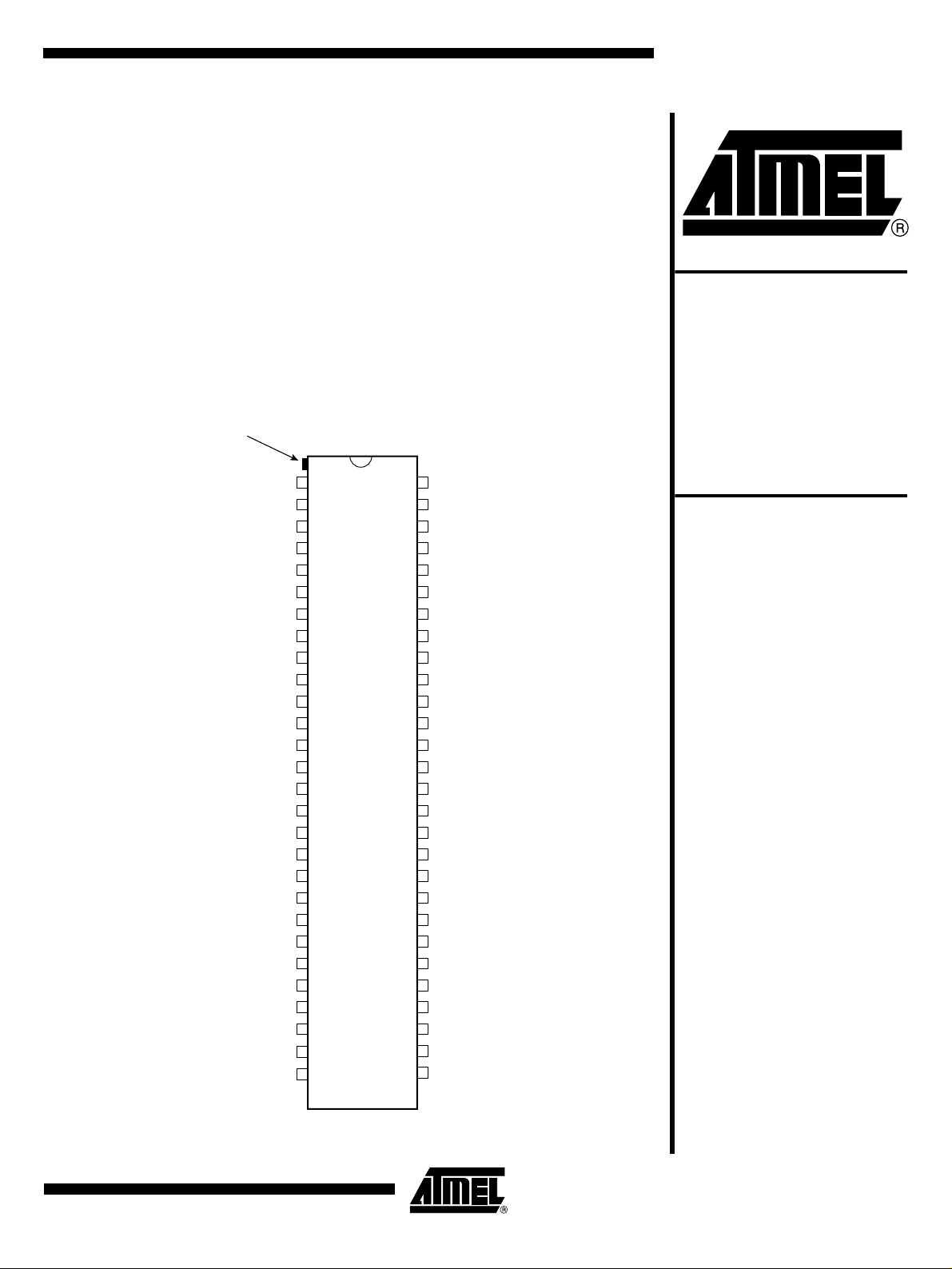
TH7834C
TOP VIEW
Rev. 1997A–IMAGE–05/02
1
Page 2

Pin Description
Pin Number Symbol Designation
1V
2V
3V
4 Φ
5, 9, 14, 15, 20, 24, 33,
OS1
DR1
S1
R1-2
V
SS
Output 1 (Odd Pixels)
Reset DC Bias (Output 1)
Amplifier Source Bias (Output 1)
Reset Clock (Outputs 1 and 2)
Substrate Bias (Ground)
37, 42, 43, 48, 52
6, 34 VST Pixel Storage Gate DC Bias
7 Φ
8V
10 Φ
11 Φ
12 Φ
13 Φ
16 Φ
17 Φ
18 Φ
19 Φ
21 Φ
22 VA
23 Φ
25 V
26 V
27 V
28 V
29 V
30 V
31 V
32 Φ
35 Φ
36 V
38 Φ
39 Φ
40 Φ
41 Φ
44 Φ
45 Φ
A1-2
GS1-2
3A
1A
4A
2A
2C
4C
1C
3C
P3-4
3-4
LS3-4
DD3-4
S3
DR3
OS3
OS4
DR4
S4
R3-4
A3-4
GS3-4
3D
1D
4D
2D
2B
4B
Antiblooming and/or Exposure Time Control
Output Gate DC Bias
Register Main Transport Clock
Register Main Transport Clock
Register Main Transport Clock
Register Main Transport Clock
Register Main Transport Clock
Register Main Transport Clock
Register Main Transport Clock
Register Main Transport Clock
Transfer Clock
Antiblooming Diode Bias
Register End Transport Clock
Amplifier Drain Supplies (Outputs 3, 4)
Amplifier Source Bias (Output 3)
Reset DC Bias (Output 3)
Output 3 (Odd Pixels)
Output 4 (Even Pixels)
Reset DC Bias (Output 4)
Amplifier Source Bias (Output 4)
Reset Clock (Outputs 3 and 4)
Antiblooming and/or Exposure Time Control
Output Gate DC Bias
Register Main Transport Clock
Register Main Transport Clock
Register Main Transport Clock
Register Main Transport Clock
Register Main Transport Clock
Register Main Transport Clock
2
TH7834C
1997A–IMAGE–05/02
Page 3
Pin Description (Continued)
Pin Number Symbol Designation
46 Φ
47 Φ
49 Φ
50 VA
51 Φ
53 V
54 V
55 V
56 V
Notes: 1. Pins Φ
A1-2,VGS1-2
1B
3B
P1-2
1-2
LS1-2
DD1-2
S2
DR2
OS2
, Φ
P1-2
connected together inside the package.
2. Two Pins V
connected together inside the package.
ST
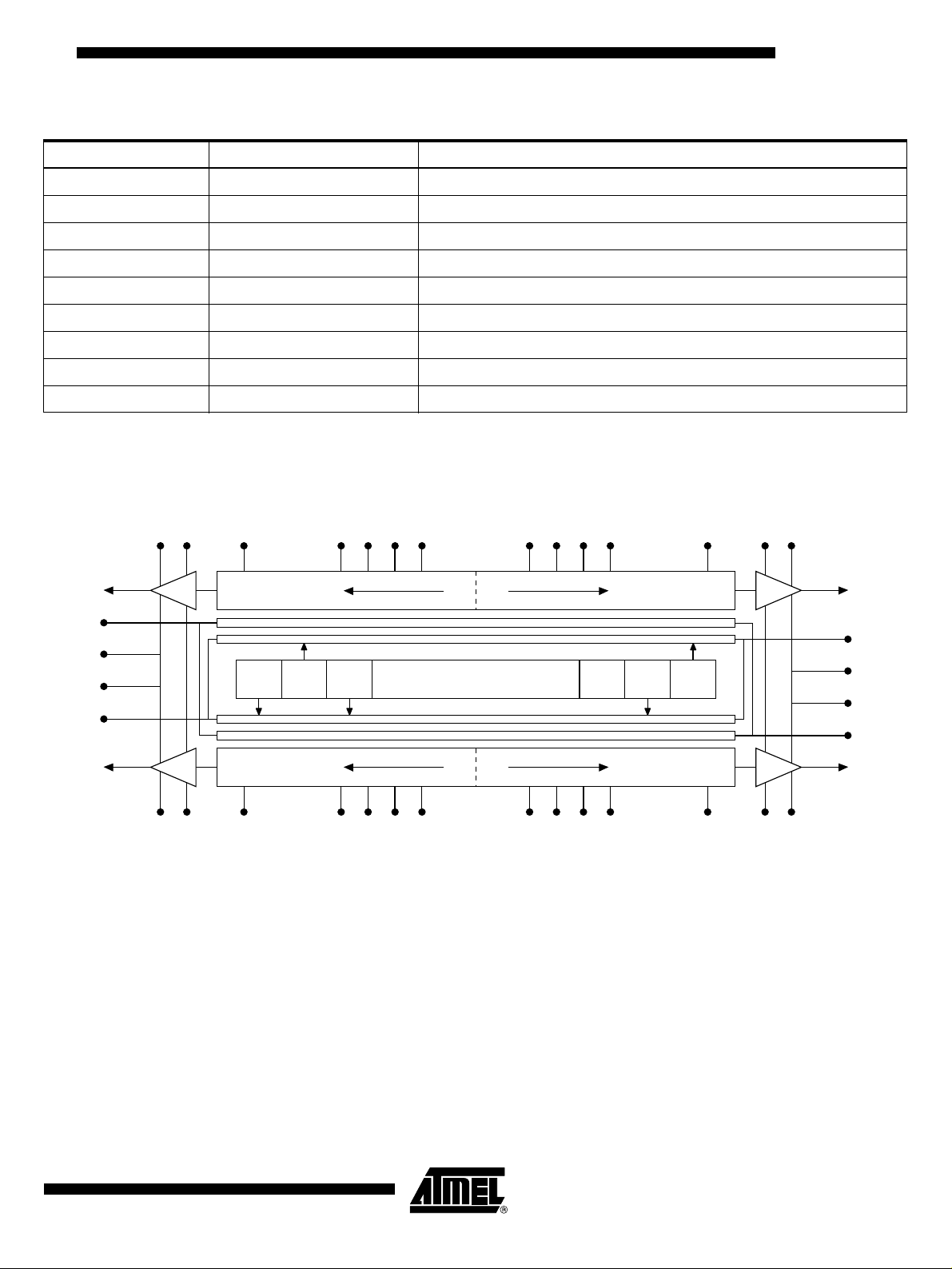
Figure 1. TH7834 Block Diagram
ΦLS1-2VDR2 VDR4VS2 VS4
,VA
1-2
, Φ
LS1-2,VDD1-2
Φ3B
Φ1B
Register Main Transport Clock
Register Main Transport Clock
Transfer Clock
Antiblooming Diode Bias
Register End Transport Clock
Amplifier Drain Supplies (Outputs 1, 2)
Amplifier Source Bias (Output 2)
Reset DC Bias (Output 2)
Output 2 (Even Pixels)
, Φ
and respectively, Φ
R1-2
Φ4B
Φ2B
Φ2D
Φ4D
A3-4,VGS3-4
Φ1D
Φ3D
, Φ
P3-4
,VA
3-4,ΦLS3-4,VDD3-4
VGS3-4
TH7834C
, Φ
are not
R3-4
VOS2 VOS4CCD B
ΦP1-2
VDD1-2
ΦR1-2
VST
VOS1 VOS3CCD A CCD C
1
Φ4A
Φ2A
Φ2C
Φ4C
Φ3C
Φ1C
VGS1-2VDR1 VDR3VS1 VS3
Φ1A
Φ3A
CCD D
VST
ΦR3-4
12000
VDD3-4
ΦP3-4
ΦLS3-4
Description TH7834C high resolution linear array consists of 12000 useful pixel photosensitive line,
associated with four CCD shi ft registers and fo ur output amplifiers. Transfer gate s on
both sides of the photosensitive line enable delivery of charges, respectively:
• on one side, charge accumulated by odd pixels (1, 3, 5… 11999), to CCD shift
registers A and C,
• on the other side, charge accumulated by even pixels (2, 4, 6… 12000), to CCD
shift registers B and D.
1997A–IMAGE–05/02
Shift registers 1 and 2 collect charges generated by one half of the photosensitive line
(pixel 1 to 6000), whereas shift registers 3 and 4 collect charges generated by the second half of the photosensitive line (pixels 12000 to 6001).
3
Page 4
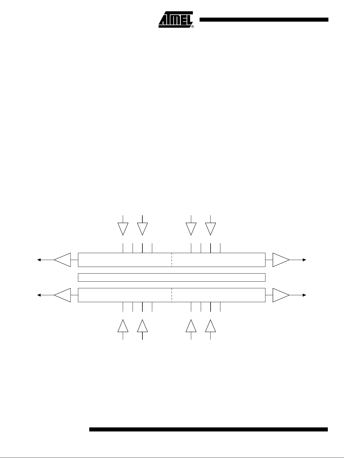
Figure 2. Driving Schematic
The four CCD shift registers have separated clocks. The output signal can be, then,
delivered simultaneously or sequentially on the four outputs.
The four CCD shift registers are designed with 4 separated gates. According to the gate
connection, the signal can be read through 2 or 4 output amplifiers.
According to gate connection, 2 or 4 output operating mode can be chosen. In the 4 output operating mode, signals associated to the end pixels of the array (either pixels
number 1, 2 or pixels number 11999, 12000) are delivered first in time and signals corresponding to the center of the line (pixels number 5999, 6000 and 6001, 6002) are
delivered last in time. Thus, external circuitry and processing are needed to combine the
four video outputs and to restore the normal order of the pixels in accordance with their
spatial distribution on the photosensitive line.
Terminal stages for every CCD shift register have separate clock control inputs in order
to speed up the final charge to voltage conversion and reduce the video output settling
time.
Antiblooming and exposure time control functions are provided.
Symmetrical TH7834 package PIN OUT allow to inverted pin 1 and 56 positions without
damage.
To obtain optimal operating mode, separated driving circuits are recommended for each
readout shift register (at least
Logical signal :
L1
Φ
L2
Φ
Logical signal :
ΦLS and ΦR).
L1
Φ
L2
Φ
Pins (1,2,3,4)B
Φ
VOS2 VOS4CCD B26000
Photosensitive line
VOS1 VOS3CCD A CCD C
1
Logical signal :
Pins (1,2,3,4)AF
L1
Φ
L2
Φ
5999
6002
6001
Pins (1,2,3,4)D
Φ
Pins (1,2,3,4)CF
L1Logical signal :
Φ
L2
Φ
CCD D
12000
11999
PHI3C
4
TH7834C
1997A–IMAGE–05/02
Page 5

TH7834C
Readout Shift Register Clocking
All gates of the 4 CCD shift registers are separated, enabling two or four output readout
modes.
To select 2 or 4 outputs operating mode, register main transport gates must be connected as described here after:
• 4 outputs mode:
V
: ΦL1= Φ2A+ Φ3A; ΦL2= Φ1A+ Φ
OS1
V
: ΦL1= Φ2B+ Φ3B; ΦL2= Φ1B+ Φ
OS2
V
: ΦL1= Φ2C+ Φ3C; ΦL2= Φ1C+ Φ
OS3
V
: ΦL1= Φ2D+ Φ3D; ΦL2= Φ1D+ Φ
OS4
• 2 output mode: VOS1andV
V
: ΦL1= Φ2A+ Φ3A+ Φ1C+ Φ
OS1
Φ
= Φ1A+ Φ4A+ Φ3C+ Φ
L2
V
: ΦL1= Φ2B+ Φ3B+ Φ1D+ Φ
OS2
Φ
= Φ1B+ Φ4B+ Φ3D+ Φ
L2
• 2 output mode: V
V
: ΦL1= Φ1A+ Φ2A+ Φ2C+ Φ
OS3
Φ
= Φ3A+ Φ4A+ Φ1C+ Φ
L2
V
: ΦL1= Φ1B+ Φ2B+ Φ2D+ Φ
OS4
Φ
= Φ3B+ Φ4B + Φ1D+ Φ
L2
OS3
and V
OS2
OS4
Note: In 2 output mode, the unused outputs can be connected as following:
• Φ
= ΦR=VGS=0V
LS
•10V<V
•V
DD
•V
not connected in order to cancel unused output amplifiers power consumption.
S
DR
=15V
<15V
4A
4B
4C
4D
:
2C
4C
2D
4D
:
3C
4C
3D
4D
Absolute Maximum Ratings*
Storage Temperature ................................... -55°C to + 150°C
Operating Temperature ................................. 0°C to + 70°C
Thermal Cycling.........................................................15°C/mm
Maximum Voltage:
• Pins: 4, 6, 7, 8, 10, 11, 12, 13, 16, 17, 18,
19, 21, 23, 32, 34, 35, 36, 38, 39, 40, 41, 44,
45, 46, 47, 49, 51...............................................-0.3V to + 15V
• Pins: 2, 3, 22, 25, 26, 27, 30,
31, 50, 53, 54, 55............................................-0.3V to + 15.5V
• Pins: 5, 9, 14, 15, 20, 24, 33, 37, 42, 43, 48, 52 .. Ground 0V
*NOTICE: Stresses above those listed under absolute max-
imum ratings may cause permanent device failure. Functionality at or above these limits is not
implied. Exposure to absolute maximum ratings
for extended periods may affect reliability.
Operating Range Operating range defines the temperature limits between which the functionality is guar-
anteed: 0°C to 70°C.
1997A–IMAGE–05/02
5
Page 6

Operating Precautions
Shorting the video outputs to VSS or VDD, even temporarily, can permanently damage
the output amplifiers.
Operating Conditions (T = 25°C)
Table 1. DC Characteristics
Parameter Symbol
Value
UnitMin. Typ. Max.
Output Amplifier Drain Supply V
DD1-2,VDD3-4
Substrate Voltage V
Reset DC Bias V
Output Amplifier Source Bias V
Output Gate DC Bias V
DR1,VDR2,VDR3,VDR4
S1,VS2,VS3,VS4
GS1-2,VGS3-4
Photosensitive Zone DC Bias V
Antiblooming Diode Bias VA
1-2
Note: If no exposure time control is required, Φ
Typical current in V
<10µA;inVGS,VST<1µA.
DR,VA
Timing Diagram
Figure 3. Line Timing Diagram
ΦP3-4ΦP1-2
ΦΦL1, L2
ΦΦLS1-2, LS3-4
SS
ST
,VA
A1-2
3-4
and Φ
14.5 15 15.5 V
00 V
VDD-0.5 V
0V
2.2 2.4 2.6 V
3.544.5V
14 14.5 15 V
must be connected to an adjustable DC bias (see Figure 7).
A3-4
External
6
ΦΦR1-2, R3-4
ΦEc1
(clamp)
ΦEch
(Sampling)
TH7834C
Detailed timing diagram
for transfert from
photosite to register
(see fig. 4)
• Minimum exposure time: Ti min = readout time.
For data rate of 5 MHz: Ti min = = 608.6 µs.
Note: It is better to clean the shift registers (with running clocks) and not to stop clocking them
Readout time for line M
Integration time Ti for line M+1
after readout time.
Detailed pixel
timing diagram
(see fig. 5)
3043
-----------------
5MHz
Pixel N
Cleaning
1997A–IMAGE–05/02
Page 7

• Each video line in four output operating mode consists in:
– 30 inactive pre-scan, (not connected to pixels),
– 6 dark references,
– 4 isolation elements, (inactive, not connected to pixels),
– 3 non-useful pixels,
– 3 000 useful pixels of the line.
TH7834C
N = number of pixel periods (T
) during readout period (see Figure 5).
p
Four output operating mode: N ≥ 3043.
Two output operating mode: N ≥ 6086.
(Φ
can be clocked during the line blancking).
LS
Figure 4. Detailed Timing Diagram For Transfer From Photosite To Register
ΦP1-2, ΦP3-4
≥ 20 ns
ΦL1, ΦL2
ΦLS
N1
ΦR
≥ 2 µs
Figure 5. Detailed Pixel Timing Diagram
ΦP1-2, ΦP3-4
ΦL1, ΦL2
ΦLS1-2, ΦLS3-4
Tp/2 Typ.
≥ 100 ns
Tp (200 ns Typ.)
ΦR1-2, ΦR3-4
VOS (1-2-3-4)
(CCD output signal)
1997A–IMAGE–05/02
≥ 20 ns
= Pixel period
T
P
Rise and fall time:
Φ
, Φ
R1-2
R3-4
Φ
, Φ
Φ
Φ
LS1-2
L1
P1-2
LS3-4
, ΦL2: 25% of TP (min. 30 ns),
, Φ
P3-4
≥ 30 ns
Reset
Signal
:5%ofTP(min. 5 ns),
:5%ofTP(min. 5 ns),
: 100 ns (min 20 ns).
Floating
diode
(Reference level for
correlated double Sampling)
7
Page 8

Table 2.
Cross over of complementary clocks (ΦL1and ΦL2) preferably at 50% of their amplitude.
Note: Generally, the difference between the floating diode level and signal level is the sum of
several signals:
• Register clock feedthrough
• Average CCD register dark signal proportional to CCD clock period, mode, temperature
• Pixel dark signal (depending upon temperature and exposure time)
• Pixel signal under illumination
Elements
Inactive
Prescan
Dark
References
Isolation
Elements
Non Useful
Pixels Useful PixelsSignals
RegisterClockFeedthrough XXXXX
AverageCCDRegisterDarkSignalXXXXX
Pixel Dark Signal X X X
Pixel Signal Under Illumination XX
Table 3. Drive Clock Voltage Swings
Value
Parameter Symbol Logic
Register Main Transport Clock
Register End Transport Clock
(1)
(1)
ΦL1, Φ
Φ
LS1-2
Φ
LS3-4
L2
,
High 8.5 9 11 V
Low 0 0.4 0.6 V
High 8.5 9 11 V
Low 0 0.2 0.4 V
High 9.5 10 10.5 V
Antiblooming (Low Level) And
Exposure Time Control (High Level)
Reset Clock
Transfer Clock
(1)
(1)
Φ
A1-2
, Φ
A3-4
Low 0
To be
adjusted
(1)
High 10.5 11 12.5 V
Φ
, Φ
R1-2
R3-4
Low 0 1.5 2 V
High 10.5 11 11.5 V
Φ
, Φ
P1-2
P3-4
Low 0 0.4 0.6 V
Note: 1. Transients under 0.0V in the clock pulseswill lead to charge injection,causing a localized increase of the dark signal. If such
spurious negative transients are present, they can be removed by inserting a serial resistor of appropriate value (typically
20 Ω to 100 Ω) at the relevant driver output.
UnitMin. Typ. Max.
V
8
TH7834C
1997A–IMAGE–05/02
Page 9

TH7834C
Table 4. Drive Clock Capacitances Operating Frequencies
(1)
Symbol Function/Clock Capacitive Network Total Max. Frequency
ΦL1 ΦL2
Φ
Φ
Φ
Φ
Φ
, Φ
L1
LS1-2
P1-2
A1-2
R1-2
, Φ
, Φ
, Φ
, Φ
L2
LS3-4
P3-4
A3-4
R3-4
160pF
Register Main Transport Clock
250pF 320pF
Register End Transfer Clock ≤ 50 pF per phase 10 MHz
ΦP
15pF
15pF
Transfer Clock 80 pF per phase
Antiblooming And Exposure
Time Control
V
ST
50pF
V
SS
15pF
Φ
A
60pF
V
SS
Reset Clock ≤ 50 pF per phase 10 MHz
Φ
Φ
for one CCD
ΦL2
V
ST
100 pF per phase
: 570 pF
L1
: 640 pF
L2
(1)
10 MHz
Pulse duration ≥ 2µs
Period: ≥ 608.6 µs
(4 outputs mode)
Note: 1. For ¼ of total CCD register.
Table 5. Static and Dynamic Electrical Characteristics
Value
Parameter Symbol
DC Output Level (Pins: 1, 28, 29, 56) V
Output Impedance (Pins: 1, 28, 29,
56)
Maximum Data Output Frequency
Per Channel
F
S
ref
Z
S
max 5 10 MHz
10 V
400 600 Ω
Input Current On Active Pins 4, 6, 7,
8, 10, 11, 12, 13, 16, 17, 18, 19, 21,
23, 32, 34, 35, 36, 38, 39, 40, 41, 44,
I
e
<< 1 2 µA
45, 46, 47, 49, 51
Amplifier Drain Supply Current (Per
)
V
DD
Static Power Dissipation (Per V
DD
I
DD1-2,IDD3-4
)P
D1-2,PD3-4
10 16 mA VDD=15V
165 240 mW
Note: The maximum clock frequency is limited by the dark signal increase. Full performance for 5 M Hz.
Unit RemarksMin. Typ. Max.
(Note:)
V
=15V
in
with all other
pins = 0V
1997A–IMAGE–05/02
9
Page 10

Electro-optical
• General measurement conditions: Tc = 25°C; Ti = 1 ms; FΦLA,FΦLB,FΦLC,FΦLD=
Performance
• Light source: tungsten filament lamp (2,854 K) + BG 38 filter (2 mm thick) + F/3.5
• Typical operating conditions (see Table 1, 2, 3 and 4). First and last pixels of the
• Test without antiblooming, except for AE max.
Table 6. Electro-optical Performance
5 MHz, readout through 4 outputs.
aperture. The BG 38 filter limits the spectrum to 700 nm. In these conditions,
1 µJ/cm
2
corresponds to 3.5 lux.s.
photosensitive line, as well as reference elements, are excluded from the
specification.
Value
Parameter Symbol
Saturation Output Voltage With
Antiblooming OFF
Saturation Exposure E
V
SAT
SAT
23 V
0.6 µJ/cm
Responsitivity R 3.5 5 V/µJ/cm
Photo Response Non-uniformity
Excluding Single Defects
PRNU ±6 ±10 %VOS
Unit RemarksMin. Typ. Max.
(1)(2)(3)
2
2
VOS =1.0V
Contrast Transfer Function At Nyquist
Frequency (77 Ip/mm)
at 500 nm
at 600 nm
CTF
at 700 nm
Temporal Noise In Darkness (rms) 300 µV
Dynamic Range (Relative to rms
Noise)
Pixel Average Dark Signal V
D
R
DS
75
62
47
10000
110 250 µV/ms
%
%
%
VOS = 1.5V
For white level
(5)
(6)
Dark Signal Non-uniformity DSNU 90 400 µV/ms Peak to peak
Register Single Stage Transfer
Efficiency
Lag (Vertical Charge Transfer
Efficiency)
1-ε 0.99998 0.999998 VOS
VCTE 0.1 0.5 %
Antiblooming Efficiency AE max <1 15 mV
=1V
(7)
(8)
Notes: 1. Value measured with respect to zero reference level.
2. Conversionfactor is typically: 6 µV/e-.
= Φ
3. Without antiblooming: Φ
4. VOS
= average output voltage; PRNU for each output, in 4 output operating mode.
A1-2
A3-4
=0V.
5. Measured in Correlated Double Sampling (C.D.S.) mode.
6. V
7. Residualsignal after line readout, at VOS
and DSNU vary with temperature.
DS
=1V.
8. Line acquisition with Phi-A at high level. AE max = maximum signal along the line (to test all the antiblooming sites).
(4)
(6)
10
TH7834C
1997A–IMAGE–05/02
Page 11

Figure 6. Typical Spectral Responsitivity
8.0
7.2
6.4
5.6
)
4.8
2
4.0
µ
(V/ J/cm
3.2
2.4
1.6
0.8
0
400 500 600 700 800 900 1000 1100
η=0.8
Lambda (nm)
TH7834C
η=0.7
η=0.6
Exposure Time Reduction (See Figure 8)
Figure 7. V
versus ΦALow Level Typical Curve
SAT
Antiblooming
OFF
3600
3400
3200
3000
2800
2600
2400
2200
2000
(mV)
1800
1600
Vsat.
1400
1200
1000
800
600
400
200
0
0 123456788.5
ΦA bias (V)
Antiblooming
ON
VST=4V
R Low level= 1.5V
Φ
VA= 13V
TH7834 allo ws a reduction in the expo sur e time without changing the readout time. It
thus provides a function which is equivalent to an optical iris.
The exposure time reduction consists in increasing the
Φ
gate bias in order to remove
A
continuously, during period 2, the photoelectrons from the pixel and to inject them into
the antiblooming diode V
.WhenΦAreturns to the normal bias, electrons are integrated
A
in the pixel.
1997A–IMAGE–05/02
Only excess electrons are evacuated into V
gration time is ti instead of T
transfer and reset clocks (
, without any ch an ge in the readout sequence . Register
i
Φ
, ΦLSand ΦR) must be pulsed during the Tiintegration time.
L
(blooming control). Thus, the actual inte-
A
11
Page 12

Table 7. Exposure Time Reduction Conditions
Parameter Symbol
Value
UnitMin. Typ. Max.
Antiblooming Diode Bias VA
Antiblooming And Expose Time
.VA
1-2
3-4
Φ
, Φ
A1-2
A3-4
14 15.5 15 V
to be adjusted V
Control
Period 1
Period 2 9.5 10 10.5 V
Figure 8. Timing Diagram For Exposure Time Control
ΦP(1-2, 3,4)
Clear period
Φ A(1-2, 3,4)
0V
Antiblooming
level
Period 2
≥T
R
Period 1
integration time t
Note: It is better to have ΦAfalling/rising edge outside the useful readout period.
Outline Drawing
PIXEL1
2.54 ± 0.25
MARK
∆t ≥ 20ns
i
TR= Readout period
±0.32
1.10 ± 0.10
3.15
0.27
1
2.12 ±
3.2 4.2
68.58 0.25
(2.54±×27)
88.0 ±0.88.
7.50 ± 0.10
9.71 0.6±
1.27 ± 0.25
Y
5.00 0.10±
X
1st pixel
Note: Antireflective window: reflection.
Less than 1% per side over 400 - 700 nm wavelength range.
All dimensions are in mm (except otherwise specified).
Ordering Code The ordering code is TH7834CCC-RB
pixel 12000
|Y12000-Y1| ≤ 150 µm
4.35 ± 0.45
15.24 ±0.25
Z=1.80±0.30
1
Window
2
Photosensitive area
3
Optical distance between
external face of window
and photosensitive
3
2
area
12
TH7834C
1997A–IMAGE–05/02
Page 13

Atmel Headquarters Atmel Operations
Corporate Headquarters
2325 Orchard Parkway
San Jose, CA 95131
TEL 1(408) 441-0311
FAX 1(408) 487-2600
Europe
Atmel Sarl
Route des Arsenaux 41
Case Postale 80
CH-1705 Fribourg
Switzerland
TEL (41) 26-426-5555
FAX (41) 26-426-5500
Asia
Room 1219
Chinachem Golden Pla za
77 Mody Road Tsimhatsui
East Kowloon
Hong Kong
TEL (852) 2721-9778
FAX (852) 2722-1369
Japan
9F, Tonetsu Shinkawa Bldg.
1-24-8 Shinkawa
Chuo-ku, Tokyo 104-0033
Japan
TEL (81) 3-3523-3551
FAX (81) 3-3523-7581
Memory
2325 Orchard Parkway
San Jose, CA 95131
TEL 1(40 8) 4 41- 031 1
FAX 1(408) 436-4314
Microcontrollers
2325 Orchard Parkway
San Jose, CA 95131
TEL 1(40 8) 4 41- 031 1
FAX 1(408) 436-4314
La Chantrerie
BP 70602
44306 Nantes Cedex 3, France
TEL (33) 2-40-18-18-18
FAX (33) 2-40-18-19-60
ASIC/ASSP/Smart Cards
Zone Industrielle
13106 Rousset Cedex, France
TEL (33) 4-42-53-60-00
FAX (33) 4-42-53-60-01
1150 East Cheyenne Mtn. Blvd.
Colorado Springs, CO 80906
TEL 1(71 9) 5 76- 330 0
FAX 1(719) 540-1759
Scottish Enterprise Technology Park
Maxwell Building
East Kilbride G75 0QR, Scotland
TEL (44) 1355-803-000
FAX (44) 1355-242-743
RF/Automotive
Theresienstrasse 2
Postfach 3535
74025 Heil bro nn, Germany
TEL (49) 71-31-67-0
FAX (49) 71-31-67-2340
1150 East Cheyenne Mtn. Blvd.
Colorado Springs, CO 80906
TEL 1(71 9) 5 76- 330 0
FAX 1(719) 540-1759
Biometrics/Imaging/Hi-Rel MPU/
High Speed Converters/RF Datacom
Avenue de Rochepleine
BP 123
38521 Sai nt-E grev e C edex , F ra nce
TEL (33) 4-76-58-30-00
FAX (33) 4-76-58-34-80
e-mail
literature@atmel.com
Web Site
http://www.atmel.com
© Atmel Corporation 2002.
Atmel Corporation makes no warranty for the use of its products, other than those e xpressly contained in the Company’s standard warranty
which is detailed in Atmel’s Terms and Conditions located on the Com pany’s web site. The Company assumes no responsibility for any errors
which may appear in this document, reserves the right to change devices or spec ifications detailed herein at any time w ithout notice, and does
not make any commitment to update the information contained herein. No licenses to patents or other intellectual property of Atmel are granted
by the Company in connection with the sale of Atmel products, expressly or by implication. Atmel’s products are not authorized for use as critical
components in life support devices or systems.
ATMEL®is the registered trademarks of Atmel.
Other te rms and product names may be the tradema rks of others.
Printed on recycled paper.
1997A–IMAGE–05/02
0M
 Loading...