

Page 1
Features
• Data Rate up to 50 MHz (2 Outputs at 25 MHz Each)
• Pixel Size: 10 µm x 10 µm (10 µm Pitch)
• 300 to 1100 nm Spectral Range
• High Sensitivity and Lag-free Photodiodes
• Very Low Noise (30 pJ/cm
• Antiblooming
• Exposure Control
• 20-lead 0.4" DIL Package
• Electrical, Mechanical and Optical Compatibility Between the TwoProducts
The TH7813 and TH7814 linear arrays are based on Atmel’s most recent know-how in
terms of design and technology. Flexibility and performance of these devices give the
opportunity to use them in most vision systems for industrial applications (web inspection, process control, sorting and inspection of various parts), document scanning up
to 200 dpi, metrology,etc.
2
Noise Equivalent Illumination)
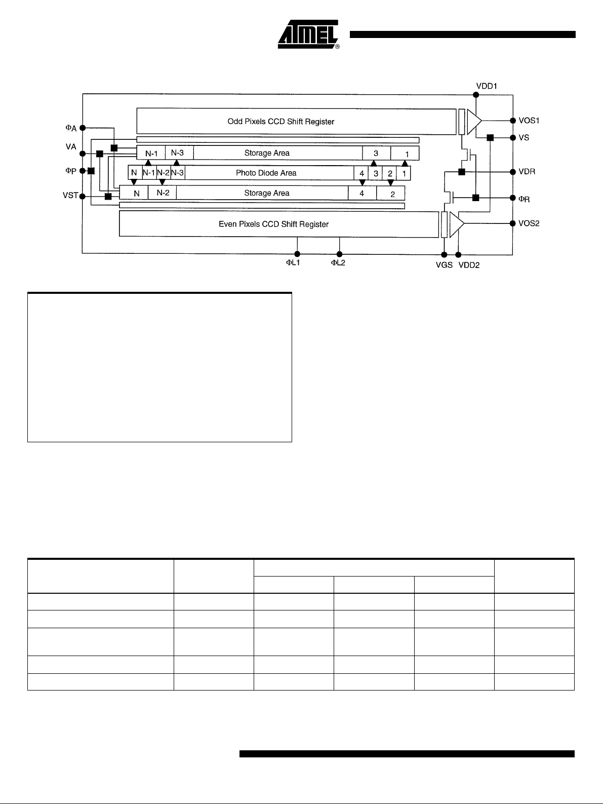
Pin Identification
50 MHz
1024/2048
Linear CCDs
All pins must be connected
Pin Number Symbol Function
4, 17 VDD1,2 Output Amplifiers Drain Supply
3, 18 VOS1,2 Video Outputs
5 VS Output Amplifiers Substrate Bias
20 VDR Reset Drain Supply
2 VGS Output Gate Bias
14 ΦL1
13 ΦL2
15 ΦR ResetClock
10 ΦA Antiblooming Gate Bias/Clock
7 VA Antiblooming Drain Bias
8 VST Storage Gate Bias
11 ΦPTransferGateClock
1, 6, 9, 12, 16, 19 VSS
TH7813A
TH7814A
Readout Register Clocks
Ground, Optical Shield Grounding
(Internally Connected)
VSS
VGS
VOS1
VDD1
VS
VSS
VA
VST
VSS
ΦA
1
2
3
4
5
TH7813A
TH7814A
6
7
8
9
10
20
19
18
17
16
15
14
13
12
11
VDR
VSS
VOS2
VDD2
VSS
ΦR
ΦL1
ΦL2
VSS
ΦP
Rev. 1990A–IMAGE–05/02
1
Page 2
Absolute Maximum Ratings*
Storage Temperature Range......................... -55°C to +150°C
Operating Temperature Range........................ -40°C to +85°C
Thermal Cycling..........................................................15°C/mn
Maximum Applied Voltages:
• Pin: 2, 8, 10, 11, 13, 14, 15 ..................................-0.3 to 15V
• Pin: 4, 5, 7, 17, 20 ................................................-0.3 to 16V
• Pin: 1, 6, 9, 12, 16, 19 .........................................0V (ground)
Note: Operating range defines the limits within which the functionality is guaranteed.
Electrical limits of applied signals are given in operating conditions section.
Operating Precautions Shorting the video outputs to any other pin, even temporarily, can permanently damage
the on-chip output amplifier.
Operating Conditions
Table 1. DC Characteristics
*NOTICE: Stresses above those listed under absolute max-
imum ratings may cause permanent device failure. Functionality at or above these limits is not
implied. Exposure to absolute maximum ratings
for extended periods may affect device reliability.
Value
Parameter Symbol
Output Amplifier Drain Supply VDD1, VDD2 14.5 15 15.5 V
Storage Gate Bias VST 2.2 2.4 2.6 V
Antiblooming Gate (See Pixel
Saturation Adjustment)
Reset Bias VDR 13.5 14 14.5 V
Antiblooming Diode Bias VA 14.5 15 15.5 V
2
TH7813A/TH7814A
ΦA247V
1990A–IMAGE–05/02
UnitMin Typ Max
Page 3
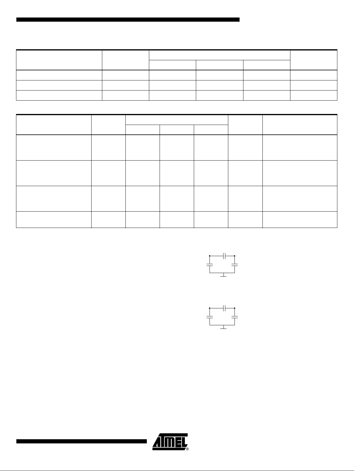
Table 1. DC Characteristics (Continued)
TH7813A/TH7814A
Value
Parameter Symbol
Register Output Gate Bias VGS 2.2 2.4 2.6 V
Output Amplifier Source Supply VS 0 V
Ground VSS 0
Table 2. Drive Clocks Characteristics
Value
Parameter Symbol
Reset gate
High level
Low level
Transfer gate
High level
Low level
Readout register clocks
Hilgh level
Low level
Maximum readout register
frequency
ΦR
ΦP
ΦL1, 2
F
H
8.5
-0.1
8.5
-0.1
8.5
-0.1
9
0
9
0
9
0
10 25 MHz
9.5
0.4
9.5
0.4 V
9.5
0.4 V
Unit RemarkMin. Typ. Max.
V
V
V
V
Clock Capacitance < 25 pF
Clock Capacitance < 100 pF
see Figure 1 and Figure 2
UnitMin Typ Max
Figure 1. Readout Register Clocks Capacitance TH7813
ΦL1 ΦL2
50 pF
140 pF120 pF
Figure 2. Readout Register Clocks Capacitance TH7814
ΦL1 ΦL2
100 pF
230 pF230 pF
1990A–IMAGE–05/02
3
Page 4

Timing Diagrams The following diagram shows the general clocking scheme for the TH7813A and
TH7814A.
Thelineiscomposedasfollows:
Number of Prescan
Synopsis
TH7813A 4 512 516
TH7814A 4 1024 1028
Pixels Per Output
Number of Useful
Pixels Per Output
Total Number of
Pixels Per Output
Postscan elements may be added in order to either increase the expos ure ti me, o r to
provide a voltage reference level.
Figure 3. Line Timing Diagram
Line Period
A
P
L1
L2
R
Transfer Period
The following diagram shows the timing for the transfer period:
Figure 4. Line Transfer Period
> 300 ns
(700 ns typ.)
> 10 ns> 10 ns
A
P
L1
L2
R
first prescan pixe
ΦR clock may also be held in high state during line transfer period.
The following diagram shows the detailed timing for the pixel readout:
l
4
TH7813A/TH7814A
1990A–IMAGE–05/02
Page 5

Figure 5. Pixel Readout Timing Diagram
L1
L2
0 ns
Tpixel
10%
90%
90%
10%
TH7813A/TH7814A
tr
tf
±
Duty cycle: 50% ± 10%
Crossover at 50%
Rise and fall time
± 10%
10 ns
R
floating
VIDEO OUTPUTS
Exposure Time Reduction
50%
10 ns
diode level
Reset Feedthrough
Offset in darkness
Video signal
The antiblooming structure of the TH7813A and TH7814A provides an electronic shutter
capability by clocking phase fA during the line period. The timing diagram is described
Rise and fall time 8 ns
Video outputs are synchronous
Video signal occurs on L2 falling edge
First useful pixel occurs on 5th
falling edge of L2 after P
below:
Antiblooming Gate ΦA Min Typ Max Unit Clock Capacitance (see note)
High Level 8.5 9 9.5 V Low Level Sets Saturation Level
Low Level 2 4 7 V See Pixel Saturation Adjustment
Pulse Min. 200 ns
Note: Clock capacitance: TH7813A = 50 pF, TH7814A = 100 pF
1990A–IMAGE–05/02
5
Page 6

Figure 6. Exposure Time Reduction
Electro-optical Performance
Line Peri
A
Φ
P
Φ
L1
Φ
L2
Φ
R
Φ
100 ns
≥
od
exposure tim
e
Transfer Peri
od
• General test conditions:
T
=25°C
CASE
Light source: 2854K with 2 mm BG38 filter (unless specified) + F/11 optical aperture.
Typical operating conditions: 2 x 10 MHz
All values are referred to prescan pixels level.
Value
Parameter Symbol
Saturation Output Voltage V
Responsivity R 7.5 8.5 V/µJ/cm
Responsivity Unbalance 2 5 %
Photo Response Non Uniformity Peak-to-peak PRNU ±5 ±10 %V
Dark Signal DS 0.1 0.4 mV/ms
Dark Signal Non Uniformity (1σ) DSNU 0.1 mV/ms
Temporal RMS Noise in Darkness V
Dynamic Range DR 5,500 6,600
CTF CTF 65 %
LAG LAG 1 %
Charge Transfer Inefficiency (per stage) HCTI 8.10
SAT
N
1.65 2 3 V
300 µV
-5
Unit RemarksMin Typ Max
OS
2
VOS=50mVto1.5V
6
TH7813A/TH7814A
1990A–IMAGE–05/02
Page 7

Static And Dynamic Electrical Characteristics
TH7813A/TH7814A
Value
Parameter Symbol
Output Amplifier Supply Current I
Output Impedance Z
DC Output Level V
Output Conversion Factor CVF 5 µV/eOffset in Darkness DC off 30 mV
Reset Feedthrough Vft 400 mV
Electro-optical
Performances
without Infrared Cut-
The TH7813A and TH7814A special semiconductor process enables to exploit the silicon's high near infrared sensiti vity while maintaining good imaging performances in
terms of response uniformity and r esolution. Typical changes in performance with and
without IR filtering are summarized below:
DD
S
REF
200 225 259 Ω
10 mA peramplifier
10 V
Unit RemarksMin Typ Max
off Fi lter
Parameter With IR Cut-off Filter Without IR Cut-off Filter
Average Video Signal Due to a Given Illumination V
PRNU (Single Defects Excluded) ±5% 5%
CTF at Nyquist Frequency 65% 49%
OS
6xV
OS
Pixel Saturation Adjustment
The TH7813A and TH7814A antiblooming structure can be used to adjust the maximum
saturation voltage, by adjusting the ΦA bias voltage. The following curve shows the relation between V
and VΦA.
SAT
Figure 7. Pixel Saturation vs. Antiblooming Bias (Typical Conditions)
Typical conditions
3
2
(V)
1
Saturation Voltage
0
234567
(V)
Antiblooming Bias
1990A–IMAGE–05/02
7
Page 8

Spectral Responsivity The following curve shows the typical responsivity for TH7813A and TH7814A.
Figure 8. Spectral Responsivity
12
10
8
)
2
6
(V/µJ/cm
Responsivity
4
2
0
200 300 400 500 600 700 800 900 1000 1100
Wavelength (nm )
8
TH7813A/TH7814A
1990A–IMAGE–05/02
Page 9

Package Drawing
Both devices have the same optical center
3
4
Z = 2.01±0.30
TH7813A/TH7814A
Z = 1.61±0.30
0.9±0.1
Notes: 1. Window
2. Photosensitive area
3. Optical distance between external face of window and photosensitive area
4. Optical distance between backside of package and photosensitive area
5. First pixel position (mm):
TH7813A TH7814A
X = 9.6 ± 0.4 X = 4 .5 ± 0.4
Y = 5.2 ± 0.35 Y = 5.2 ± 0.35
Ordering Code TH7813ACC
TH7814ACC
1990A–IMAGE–05/02
9
Page 10

Atmel Headquarters Atmel Operations
Corporate Headquarters
2325 Orchard Parkway
San Jose, CA 95131
TEL 1(408) 441-0311
FAX 1(408) 487-2600
Europe
Atmel Sarl
Route des Arsenaux 41
Case Postale 80
CH-1705 Fribourg
Switzerland
TEL (41) 26-426-5555
FAX (41) 26-426-5500
Asia
Room 1219
Chinachem Golden Plaza
77 Mody Road Tsimhatsui
East Kowloon
Hong Kong
TEL (852) 2721-9778
FAX (852) 2722-1369
Japan
9F, Tonetsu Shinkawa Bldg.
1-24-8 Shinkawa
Chuo-ku, Tokyo 104-0033
Japan
TEL (81) 3-3523-3551
FAX (81) 3-3523-7581
Memory
2325 Orchard Parkway
San Jose, CA 95131
TEL 1( 40 8) 441-0 311
FAX 1(408) 436-4314
Microcontrollers
2325 Orchard Parkway
San Jose, CA 95131
TEL 1( 40 8) 441-0 311
FAX 1(408) 436-4314
La Chantrerie
BP 70602
44306 Nantes Cedex 3, France
TEL (33) 2-40-18-18-18
FAX (33) 2-40-18-19-60
ASIC/ASSP/Smart Cards
Zone Industrielle
13106 Rousset Cedex, France
TEL (33) 4-42-53-60-00
FAX (33) 4-42-53-60-01
1150 East Cheyenne Mtn. Blvd.
Colorado Springs, CO 80906
TEL 1( 71 9) 576-3 300
FAX 1(719) 540-1759
Scottish Enterprise Technology Park
Maxwell Building
East Kilbride G75 0QR, Scotland
TEL (44) 1355-803-000
FAX (44) 1355-242-743
RF/Automotive
Theresienstrasse 2
Postfach 3535
74025 Heilbronn, Ger many
TEL (49) 71-31-67-0
FAX (49) 71-31-67-2340
1150 East Cheyenne Mtn. Blvd.
Colorado Springs, CO 80906
TEL 1( 71 9) 576-3 300
FAX 1(719) 540-1759
Biometrics/Imaging/Hi-Rel MPU/
High Speed Converters/RF Datacom
Avenue de Rochepleine
BP 123
38521 Saint-Egr eve Cedex , France
TEL (33) 4-76-58-30-00
FAX (33) 4-76-58-34-80
e-mail
literature@atmel.com
Web Site
http://www.atmel.com
© Atmel Corporation 2002.
Atmel Corporation makes no warranty for the use of its products, other t han those e xpressly contained in the Company’s standard warranty
which is detailed in Atmel’s Terms and Conditions located on t he Company’s web site. The Company assumes no responsibility for any errors
which may appear in this document, reserves the right to change devices or specifications det ailed herein at any time without notice, and does
not make any commitment to update the information contained herein. No licenses to patents or other intellectual property of Atmel are granted
by the Company in connection wit h the s ale of Atmel p roducts, expressly or by implication. Atmel’s products are not aut horized for use as critical
components in life support devices or systems.
ATMEL®is the registered t rademarks of Atmel.
Other terms and product names may be the trademarks of ot hers.
Printed on recycled paper.
1990A–IMAGE–05/02
0M
 Loading...