

Page 1
Features
• Pixel Size: 13 µm x 13 µm (13 µm pitch)
• High Data Output Rate: 20 MHz typ
• High Responsivity and Resolution over a Wide Spectral Range: from Blue (400 nm) up
to Near Infrared (1100 nm)
• Improved Dark Signal and Photo Response Uniformity
• Low Temporal Noise and High Dynamic Range: Over 6000/1
• Ease and Flexibility of Operation:
– Only two External Basic Drive Clocks
– Internal or External Sample and Reset Clocks
• 24-lead DIL Package
Pin Identification
Pin Number Symbol Designation
1V
2 Φ
3SΦ
4 Φ
8V
OSA
ECHA
ECHA
RA
DD
9TP3TestPoint3
10 TP2 Test Point 2
11 VT Register And Photosensitive Zone DC Bias
Video Output Signal A (Odd Channel)
A Channel Sample-and-hold Gate Input
A Channel Internal Sample Clock-output
A Channel External Reset Clock Input
Output Amplifier Drain And Internal Logic Supply
Linear Charged
Couple Device
(CCD) Image
Sensor 1024
Pixels
TH7804A
12 TP1 Test Point 1
13 V
15 Φ
16 Φ
17 V
18 Φ
19 V
21 SΦ
22 Φ
23 V
24 V
SS
P
T
GS
RB
INH
ECHB
ECHB
OSB
DR
Substrate Bias (Ground)
Transfer Clock
Register Transport Clock
Output Gate DC Bias
B Channel External Reset Clock Input
Internal Sample Clock Inhibition
B Channel Internal Sample Clock Input
B Channel Sample-and-hold Gate Input
Video Output Signal B (Even Channel)
Reset DC Bias
5, 6, 7, 14, 20 DNC Do Not Connected
S
V
OSA
ECHA
ECHA
RA
DNC
DNC
DNC
V
DD
TP3
TP2
TP1
1
2
3
4
5
6
7
8
9
10
11
V
T
12
TH7804A
24
23
22
21
20
19
18
17
16
15
14
13
V
DR
V
OSB
ECHB
S
DNC
V
INH
RB
V
GS
T
P
DNC
V
SS
ECHB
Rev. 1989A–IMAGE–05/0 2
1
Page 2
Absolute Maximum Ratings*
Storage Temperature ..................................... -55°Cto+150°C
Operating Temperature ....................................... 0°Cto+70°C
Thermal Cycling..........................................................15°C/mn
Maximum Voltage:
• Pins: 2, 4, 8,12,15,16,18,19, 22, 24 ................-0.3V to +18V
• Pins: 9,10,11,17 .............................................. -0.3V to +18V
• Pin: 13 .............................................................................. 0V
*NOTICE: Stresses above those listed under absolute max-
imum ratings may cause permanent device failure. Functionality at or above these limits is not
implied. Exposure to absolute maximum ratings
for extended periods may affect device reliability.
Operating Range The operating range defines the temperature limits between which functionality is guar-
anteed: 0°Cto70°C.
Operating Precautions Shorting the video output to V
output amplifier.
or VDD, even temporarily, can permanently damage the
SS
2
TH7804A
1989A–IMAGE–05/02
Page 3
Operating Conditions (T = 25°)
Table 1 . DC Bias Characteristics
TH7804A
Value
Parameter Symbol
Output Amplifier Drain Supply V
Reset DC Bias V
Output Gate DC Bias V
Photosensitive Zone And
Register DC Bias
Substrate Bias V
DD
DR
GS
V
T
SS
14 15 16 V
VDD-2.4 VDD-2 VDD-1 V
5.5 6 6.5 V
0.95 V
TN
0.0 0.0 V
Te s t P oi n t 1 T P 1 V
TestsPoints2And3 TP2,TP3 V
Notes: 1. Nominal value of VT:
V
=6.7VifΦTclock levels are at their typical value.
TN
2. No use for operation. For testing purpose only.
VΦ T()HIGH VΦT()LOW+
TN
------------ ------------ ------------- ------------- ------------- ------- 5%±=
2
V
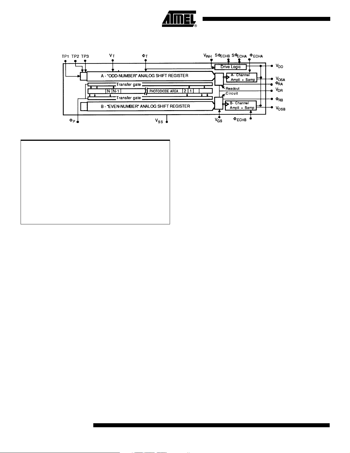
Basic Internal Configuration
SΦ
SΦ
ECHA
ECHB
and Φ
and Φ
RA
RA
internal to TH7804A
Unit RemarkMin. Typ. Max
V
TN
DD
SS
1.05 V
TN
V
V
V
(1)
(2)
(2)
Table 2 . Selection of Nominal Mode
Option Implementation Remarks
V
(19) Connected to V
INH
Internal Sampling
Internal Reset Φ
SΦ
SΦ
(3) and Φ
ECHA
(21) and Φ
ECHB
(4) and ΦRB(18) Connected to V
RA
Note: 1. Make the straps as short as possible to avoid any parasitic coupling to these connections. The load capacitance introduced
by the strap should not exceed 5 pF.
(2) Strapped
ECHA
ECHB
SS
(22) Strapped
DD
(1)
see note
1989A–IMAGE–05/02
3
Page 4
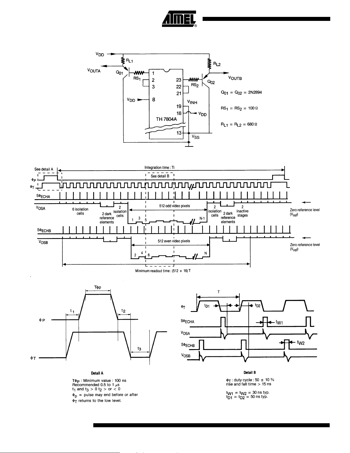
Figure 1. Basic Test Configuration
Figure 2. Timing Diagram in Basic Mode
4
TH7804A
1989A–IMAGE–05/02
Page 5
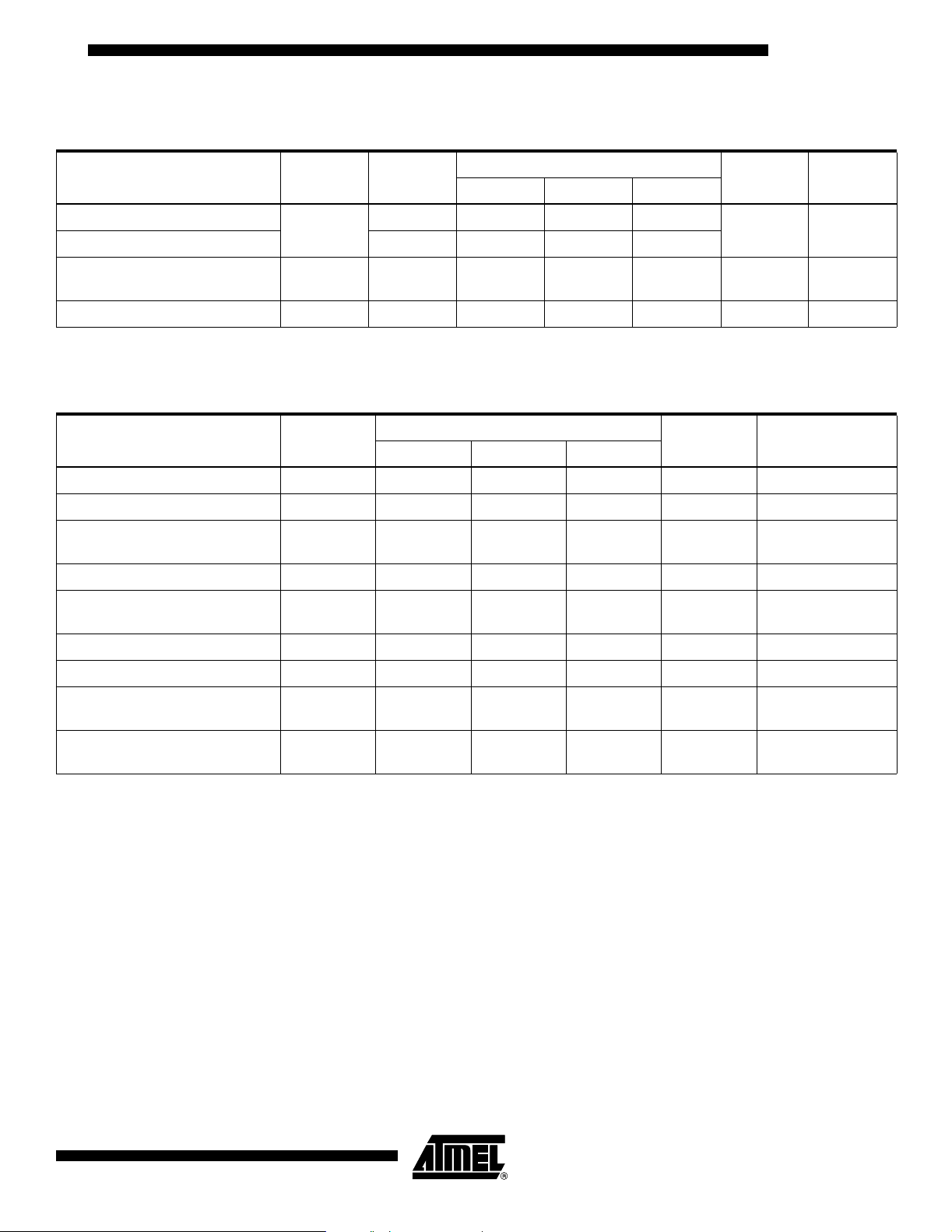
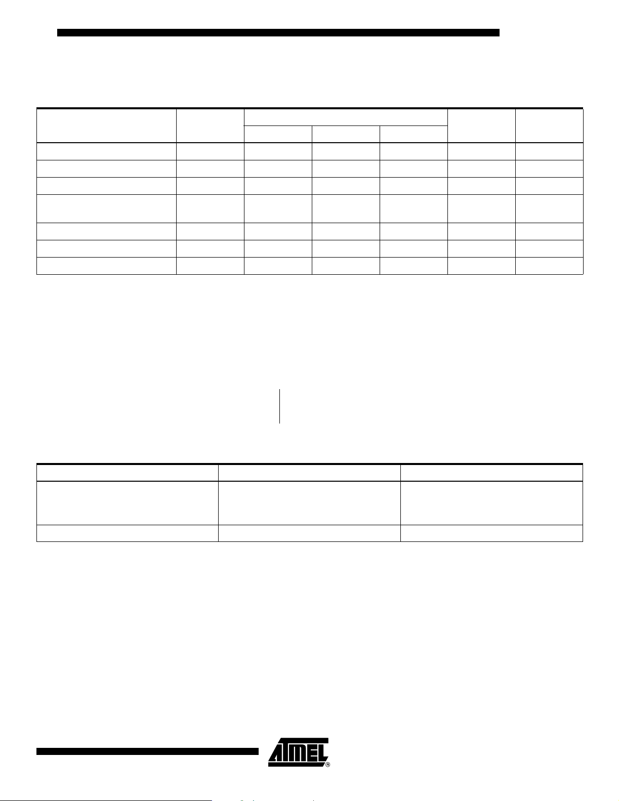
Table 3 . Drive Clock Characteristics (see Figure 2)
TH7804A
Value
Parameter Symbol Logic
Transfer Clock
Φ
, Φ
P
CΦ
T
T
P
Register Transport Clock Low 0.0 0.4 0.6
Register Transport Clock
Capacitance
Transfer Clock Capacitance CΦ
High 11 13 14
400 700 pF
130 200 pF
Unit RemarkMin. Typ. Max.
V
(1)
Note: 1. Transients under 0.0V in the clock pulses will lead to charge injection, causing a localized increase in the dark signal. If such
spurious negative transients are present, they can be suppressed by inserting a serial resistor of appropriate value (typically
20 to 100Ω) in the corresponding driver output.
Table 4 . Static and Dynamic Electrical Characteristics
Value
Parameter Symbol
DC Output Level V
Output Impedance Z
Register Single-stage Transfer
Efficiency
Max. Data Output Frequency F
Input Current On Pins: 2, 9, 10,
11, 12, 15, 16, 17, 18, 22
REF
S
CTE 99.992 99.998 % V
Smax
I
e
81012V
500 Ω
12 20 MHz
2µA
Logic RemarkMin. Typ. Max.
(1)
=1V
OS
(2)
= 15V
V
IN
All other pins: 0V
Peak Current Sink on Φ
Peak Current Sink on Φ
Clock (IΦT)
T
Clock (IΦP)
P
Output Amplifier + Internal Logic
Supply Current
Static Power Dissipation P
Notes: 1. V
2. Fs = 2 F Φ
Electro-optical Performance
= average video output voltage.
OS
. The minimum clock frequency is limited by the increase in dark signal.
T
General measurement conditions: TC=25°C; Ti=1ms;FΦT=2.5MHz(F
Light source: tungsten filament lamp (2854 K) + B6 38 filter (2 mm thick), F/3.5 aperture.
The filter limits the spectrum to 700 nm; in these conditions 1µJ/cm
lux.s.
Operating conditions (see Figure 1).
First and last pixels, as well as reference elements, are excluded from the specification.
Measurements taken on each output in succession.
P
P
I
DD
D
250 mA t
80 mA t
17 mA
255 300 mW
2
corresponds to 3.5
RISE
RISE
V
V
V
V
INH
DD
INH
DD
DATA
=15ns
=15ns
=0V
=15V
=0V
=15V
=5MHz)
1989A–IMAGE–05/02
5
Page 6
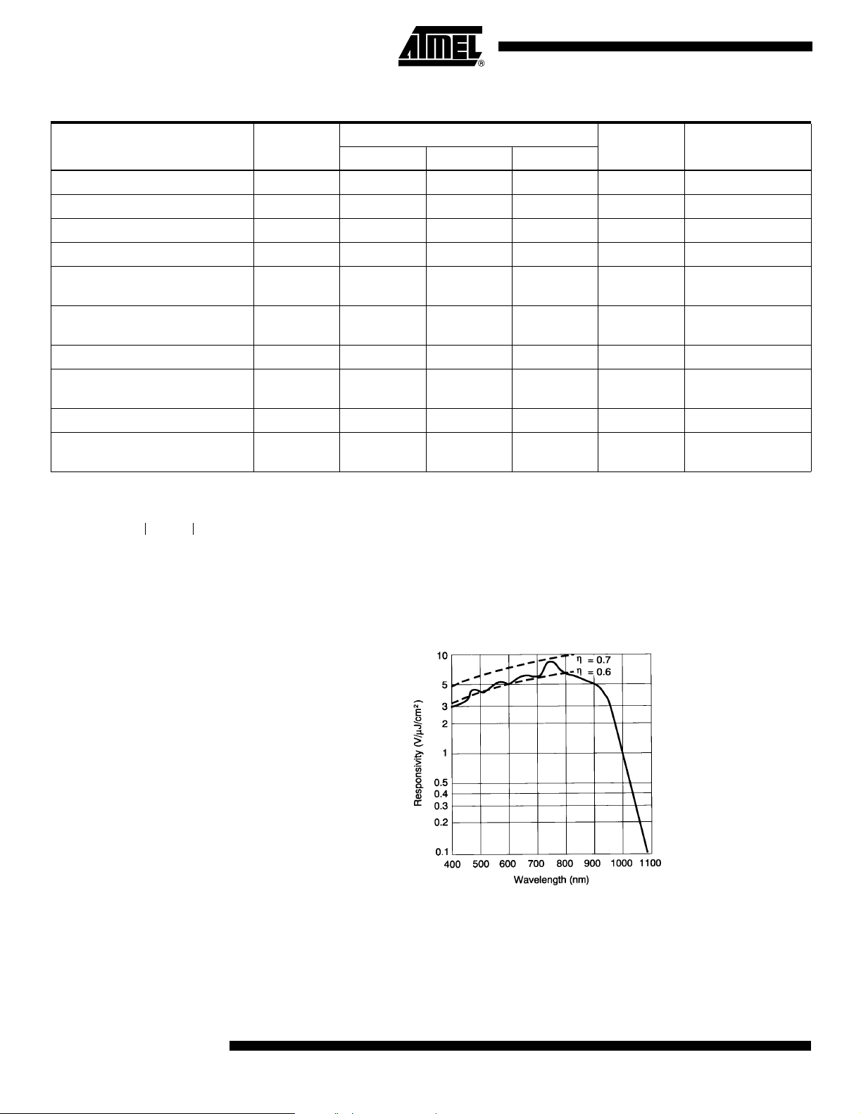
Table 5 . Electro-optical Performance
Value
Parameter Symbol
Saturation Output Voltage V
Saturation Exposure E
SAT
SAT
1.3 1.8 2.3 V
0.30 µJ/cm
Responsivity R 4.5 6 V/µJ/cm
Responsivity Unbalance ∆R/R 2 8 %
Unit RemarkMin. Typ. Max.
(1) (2)
2
2
(3)
Photo Response Non-uniformity
Peak-to-peak
Contrast Transfer Function at FN
(38 I p/mm)
PRNU ±3 ±10 % V
CTF 70 % V
Temporal Noise In Darkness 180 µV
Dynamic Range (Relative to rms
Noise)
Average Dark Signal V
Dark Signal Non-uniformity
Peak-to-peak
DR 4000 6000
DS
0.08 0.5 mV
DSNU 0.15 0.5 mV
Notes: 1. Value measured with respect to zero reference level (see Figure 2).
2. Conversion factor is typically 1.5 µV/e-.
3. ∆R/R is defined as
200 RA RB–
----------- ------------- ----------
RA RB+
where RA is responsivity of video output A, RB is responsivity of video output B.
4. Measured in Correlated Double Sampling (C.D.S.) mode.
Figure 3. Typical Spectral Response
rms
OS
VOS=50mV
to 1V
=0.9V
OS
(4)
6
TH7804A
1989A–IMAGE–05/02
Page 7
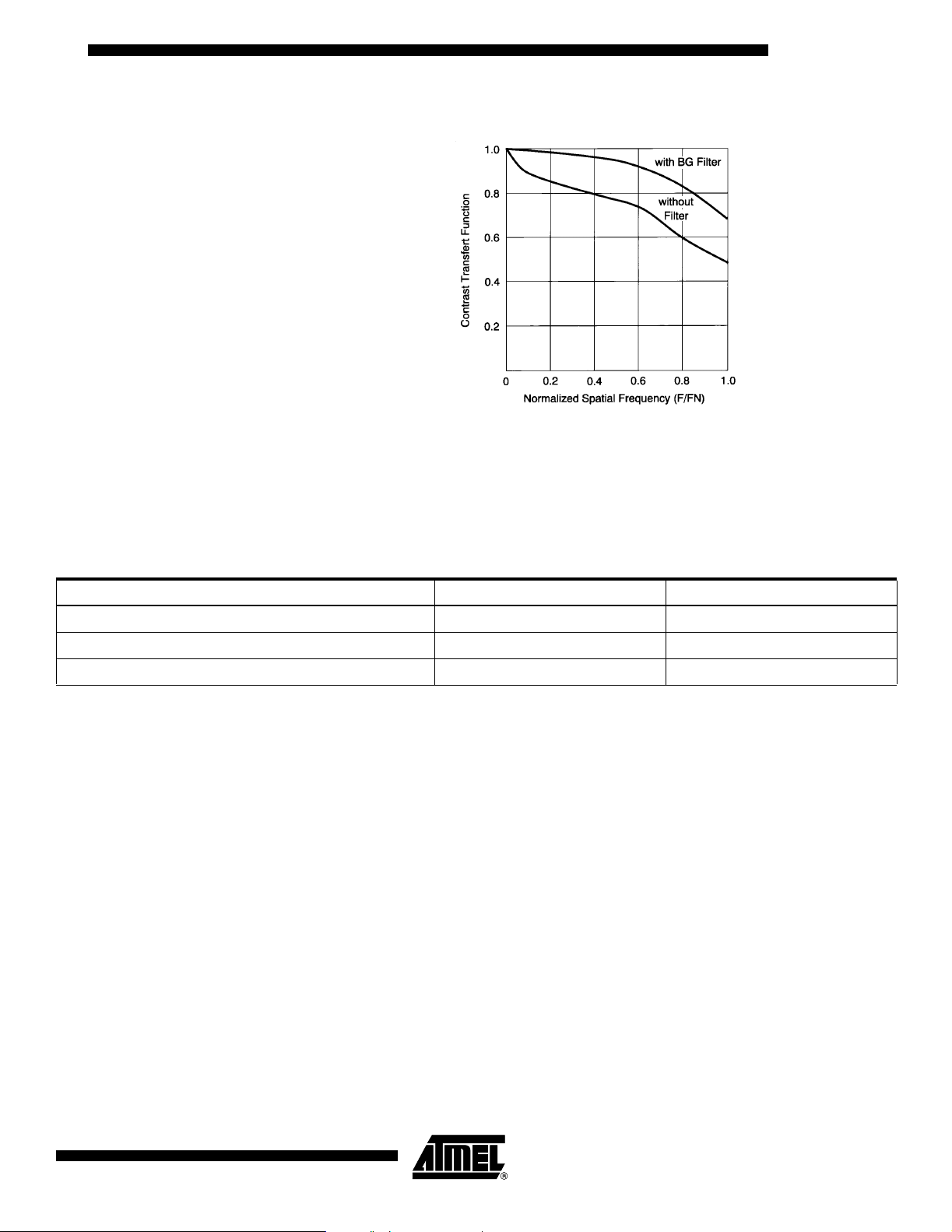
Figure 4. CTF Typical Curves (2854 K Source)
Electro-optical Performance Without Infrared Cut-off Filtering
The TH7804A’s special semiconductor process enables it to exploit the silicon's high
near infrared sensitivity while maintaining good imaging performance in terms of
response uniformity and resolution. Typical changes in performance with and without IR
filtering are summarized below.
TH7804A
With IR Cut-off Filter No IR Cut-off Filter
Average Video Signal Due to a Given Scene Illumination V
PRNU (Single Defects Excluded) ±5% ±5%
CTF at Nyquist Frequency 70% 50%
Complementary Operating Modes
TH7804A may be used in several configurations in regards to video output sampling and
charge sensing reset.
OS
VOSx4
1. Sampling Options:
Inhibition of internal sampling pulses allows for two possibilities:
a. no sampling: video output delivered in unsampled form,
b. sampling by external clocks: external sampling pulses directly applied to
Φ
, Φ
ECHA
If internal sampling clocks S
ECHB
inputs.
Φ
ECHA
and SΦ
are not used, it is recommended of
ECHB
unpower the corresponding clock drivers, as this will greatly reduce on-chip power
consumption.
2. External Reset Option:
The position and period of the charge reset clocks may be optimized by using external
clocks on
Φ
and ΦRBinputs. This is specially interesting to optimize the video outputs
RA
for Correlated Double Sampling (in order to reduce noise and improve S/N ratio).
Control signals to be applied in the different configurations are shown in Table 6.
1989A–IMAGE–05/02
7
Page 8
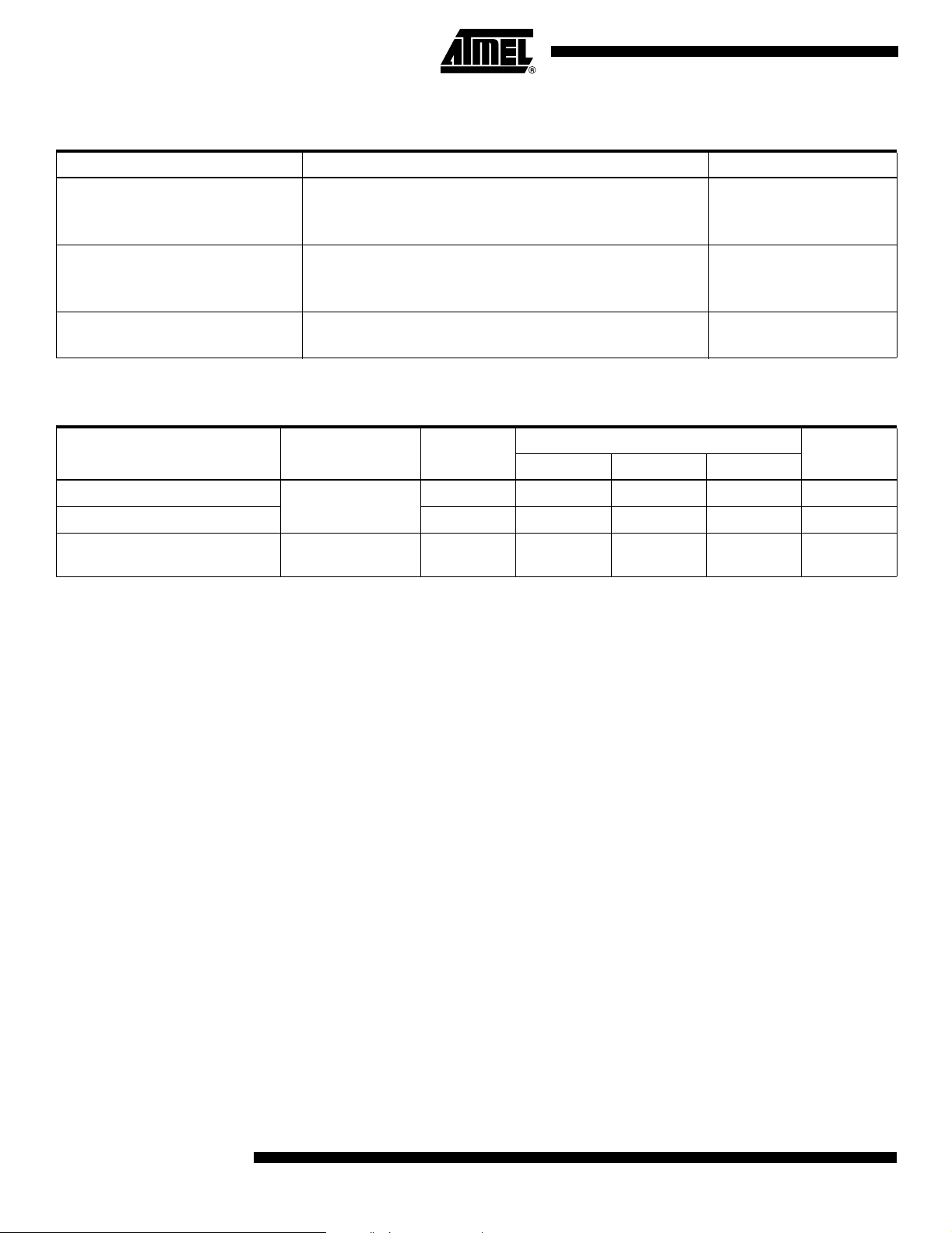
Table 6 . Selection of Operating Modes
Option Implementation Remarks
No Sampling
Sampling by External Clocks
Reset Control by External Clocks
(2) and Φ
Φ
ECHA
SΦ
V
(3) and SΦ
ECHA
(19) connected to V
INH
Sampling clocks connected to Φ
SΦ
V
Ext. Φ
Ext. Φ
and SΦ
ECHA
(19) connected to V
INH
on ΦRA(4) input
RA
on ΦRB(18)
RB
(22) connected to V
ECHB
(21) unconnected
ECHB
DD
unconnected
ECHB
DD
DD
ECHAΦECHB
(1)
seeFigure5for
sampling clock timing
(1)
seeFigure4for
reset clock timing
Note: 1. Drain supply current IDDdecreases from 10 mA to 8 mA typically when internal sampling clock is disabled.
Table 7 . External ΦRA, ΦRB, Φ
ECHA
, Φ
Clock Characteristics
ECHB
Value s
Parameter Symbol Logic
External Reset Clock
Sampling Clocks Low 0.0 0.4 0.6 V
Reset and Sampling Clock
Capacitance
CΦ
Φ
CΦ
Φ
RA
ECHA
RA
ECHA
, Φ
, Φ
,CΦ
,CΦ
RB
ECHB
RB
ECHB
High 12 12.5 13 V
10 15 pF
Insertion of a serial resistor (typically 100Ω) at the driver output avoids spurious negative transients.
UnitMin. Typ. Max.
8
TH7804A
1989A–IMAGE–05/02
Page 9

TH7804A
Figure 5. Timing Diagram — Clocks and Video Output Timing Diagram With and Without On-chip Sampling.
External reset clocks improve electro-optical performance, as listed below. Other operating conditions and other electrooptical parameters remain unchanged.
Table 8 . Performance Improvements with External ΦRAand ΦRBConfiguration
Value
Parameter Symbol
Saturation Output Voltage V
Responsivity R 8 V/µJ/cm
Dynamic Range DR 8000
SAT
2.0 V
UnitTyp.
2
Electro-optical performances obtained with complementary modes are not guaranteed for the standard products.
1989A–IMAGE–05/02
9
Page 10

Outline Drawing
Z = 1.28 ± 0.23
2.16
Notes: 1. If an optical reference is needed, it is recommended to use the window face plane.
2. Variation of Z (azimuth) on the photosensitive area of a device is ≤ ±0.1 mm.
3. Value and tolerance of Y are applicable to each individual pixel of the photosensitive line.
Ordering Code TH7804ACC
10
TH7804A
1989A–IMAGE–05/02
Page 11

Atmel Headquarters Atmel Operations
Corporate Headquarters
2325 Orchard Parkway
San Jose, CA 95131
TEL 1(408) 441-0311
FAX 1(408) 487-2600
Europe
Atmel Sarl
Route des Arsenaux 41
Case Postale 80
CH-1705 Fribourg
Switzerland
TEL (41) 26-426-5555
FAX (41) 26-426-5500
Asia
Room 1219
Chinachem Golden Plaza
77 Mody Road Tsimhatsui
East Kowloon
Hong Kong
TEL (852) 2721-9778
FAX (852) 2722-1369
Japan
9F, Tonetsu Shinkawa Bldg.
1-24-8 Shinkawa
Chuo-ku, Tokyo 104-0033
Japan
TEL (81) 3-3523-3551
FAX (81) 3-3523-7581
Memory
2325 Orchard Parkway
San Jose, CA 95131
TEL 1(408) 441-0311
FAX 1(408) 436-4314
Microcontrollers
2325 Orchard Parkway
San Jose, CA 95131
TEL 1(408) 441-0311
FAX 1(408) 436-4314
La Chantrerie
BP 70602
44306 Nantes Cedex 3, France
TEL (33) 2-40-18-18-18
FAX (33) 2-40-18-19-60
ASIC/ASSP/Smart Cards
Zone Industrielle
13106 Rousset Cedex, France
TEL (33) 4-42-53-60-00
FAX (33) 4-42-53-60-01
1150 East Cheyenne Mtn. Blvd.
Colorado Springs, CO 80906
TEL 1(719) 576-3300
FAX 1(719) 540-1759
Scottish Enterprise Technology Park
Maxwell Building
East Kilbride G75 0QR, Scotland
TEL (44) 1355-803-000
FAX (44) 1355-242-743
RF/Automotive
Theresienstrasse 2
Postfach 3535
74025 Heilbronn, Germany
TEL (49) 71-31-67-0
FAX (49) 71-31-67-2340
1150 East Cheyenne Mtn. Blvd.
Colorado Springs, CO 80906
TEL 1(719) 576-3300
FAX 1(719) 540-1759
Biometrics/Imaging/Hi-Rel MPU/
High Speed Converters/RF Datacom
Avenue de Rochepleine
BP 123
38521 Saint-Egreve Cedex, France
TEL (33) 4-76-58-30-00
FAX (33) 4-76-58-34-80
e-mail
literature@atmel.com
Web Site
http://www.atmel.com
© Atmel Corporation 2002.
Atmel Corporation makes no warranty for the use of its products, other than those expressly contained in the Company’s standard warranty
whichisdetailedinAtmel’s Terms and Conditions located on the Company’s web site. T he Company assumes no responsibility for any errors
which may appear in this document, reserves the right to change devices or specifications detailed herein at any time without notice, and does
not make any commitment to update the information contained herein. No licenses to patents or other intellectual property of Atmel are granted
by the Company in connection with the sale of Atmel products, expressly or by implication. Atmel’s products are not authorized for use as cr itical
components in life support devices or systems.
AT ME L®is the trademarks of Atmel.
Other terms and product names may be the trademarks of others.
Printed on recycled paper.
1989A–IMAGE–05/02 0M
 Loading...