

Page 1

T89C51RD2
0 to 40MHz Flash Programmable 8-bit Microcontroller
1. Description
ATMEL Wireless and Microcontrollers T89C51RD2 is
high performance CMOS Flash version of the 80C51
CMOS single chip 8-bit microcontroller. It contains a
64 Kbytes Flash memory block for program and for data.
The 64 Kbytes Flash memory can be programmed either
in parallel mode or in serial mode with the ISP capability
or with software. The programming voltage is internally
generated from the standard VCCpin.
The T89C51RD2 retains all features of the ATMEL
Wireless and Microcontrollers 80C52 with 256 bytes of
internal RAM, a 7-source 4-level interrupt controller and
three timer/counters.
In addition, the T89C51RD2 has a Programmable
Counter Array, an XRAM of 1024 bytes, an EEPROM
of 2048 bytes, a Hardware Watchdog Timer, a more
versatile serial channel that facilitates multiprocessor
communication (EUART) and a speed improvement
2. Features
• 80C52 Compatible
• 8051 pin and instruction compatible
• Four 8-bit I/O ports (or 6 in 64/68 pins packages)
• Three 16-bit timer/counters
• 256 bytes scratch pad RAM
• 7 Interrupt sources with 4 priority levels
• ISP (In System Programming) using standard V
power supply.
• Boot FLASH contains low level FLASH
programming routines and a default serial loader
• High-Speed Architecture
• 40 MHz in standard mode
• 20 MHz in X2 mode (6 clocks/machine cycle)
• 64K bytes on-chip Flash program / data Memory
• Byte and page (128 bytes) erase and write
• 10k write cycles
• On-chip 1024 bytes expanded RAM (XRAM)
• Software selectable size (0, 256, 512, 768, 1024
bytes)
• 768 bytes selected at reset for T87C51RD2
compatibility
CC
mechanism (X2 mode). Pinout is either the standard 40/
44 pins of the C52 or an extended version with 6 ports
in a 64/68 pins package.
The fully static design of the T89C51RD2 allows to
reduce system power consumption by bringing the clock
frequency down to any value, even DC, without loss of
data.
The T89C51RD2 has 2 software-selectable modes of
reduced activity for further reduction in power
consumption. In the idle mode the CPU is frozen while
the peripherals and the interrupt system are still
operating. In the power-down mode the RAM is saved
and all other functions are inoperative.
The added features of the T89C51RD2 makes it more
powerful for applications that need pulse width
modulation, high speed I/O and counting capabilities
such as alarms, motor control, corded phones, smart card
readers.
• Dual Data Pointer
• Variable length MOVX for slow RAM/peripherals
• Improved X2 mode with independant selection for
CPU and each peripheral
• 2 k bytes EEPROM block for data storage
• 100K Write cycle
• Programmable Counter Array with:
• High Speed Output,
• Compare / Capture,
• Pulse Width Modulator,
• Watchdog Timer Capabilities
• Asynchronous port reset
• Full duplex Enhanced UART
• Low EMI (inhibit ALE)
• Hardware Watchdog Timer (One-time enabled with
Reset-Out)
• Power control modes:
• Idle Mode.
• Power-down mode.
Rev. F - 15 February, 2001 1
Page 2
T89C51RD2
• Power supply:
- M version: Commercial and industrial
4.5V to 5.5V : 40MHz X1 Mode, 20MHz X2 Mode
3V to 5.5V : 33MHz X1 Mode, 16 MHz X2 Mode
- L version: Commercial and industrial
2.7V to 3.6V : 25MHz X1 Mode, 12MHz X2 Mode
• Temperature ranges: Commercial (0 to +70°C) and industrial (-40 to +85°C).
• Packages: PDIL40, PLCC44, VQFP44, PLCC68, VQFP64
Table 1. Memory Size
PDIL40
PLCC44
Flash (bytes) EEPROM (bytes) XRAM (bytes)
VQFP44 1.4
T89C51RD2 64k 2k 1024 1280 32
TOTAL RAM
(bytes)
I/O
PLCC68
Flash (bytes)
VQFP64 1.4
EEPROM
(bytes)
XRAM (bytes)
TOTAL RAM
(bytes)
T89C51RD2 64k 2k 1024 1280 48
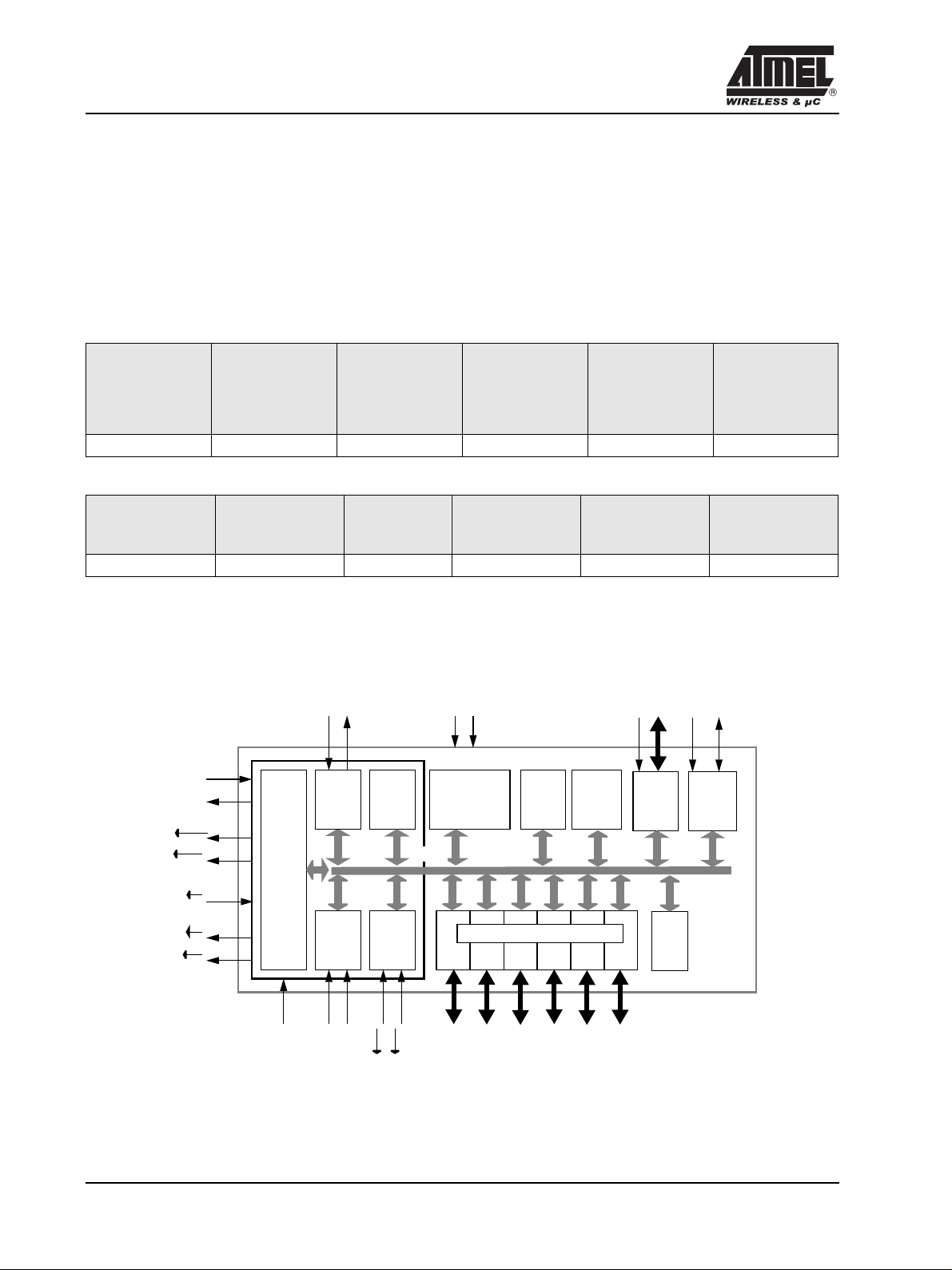
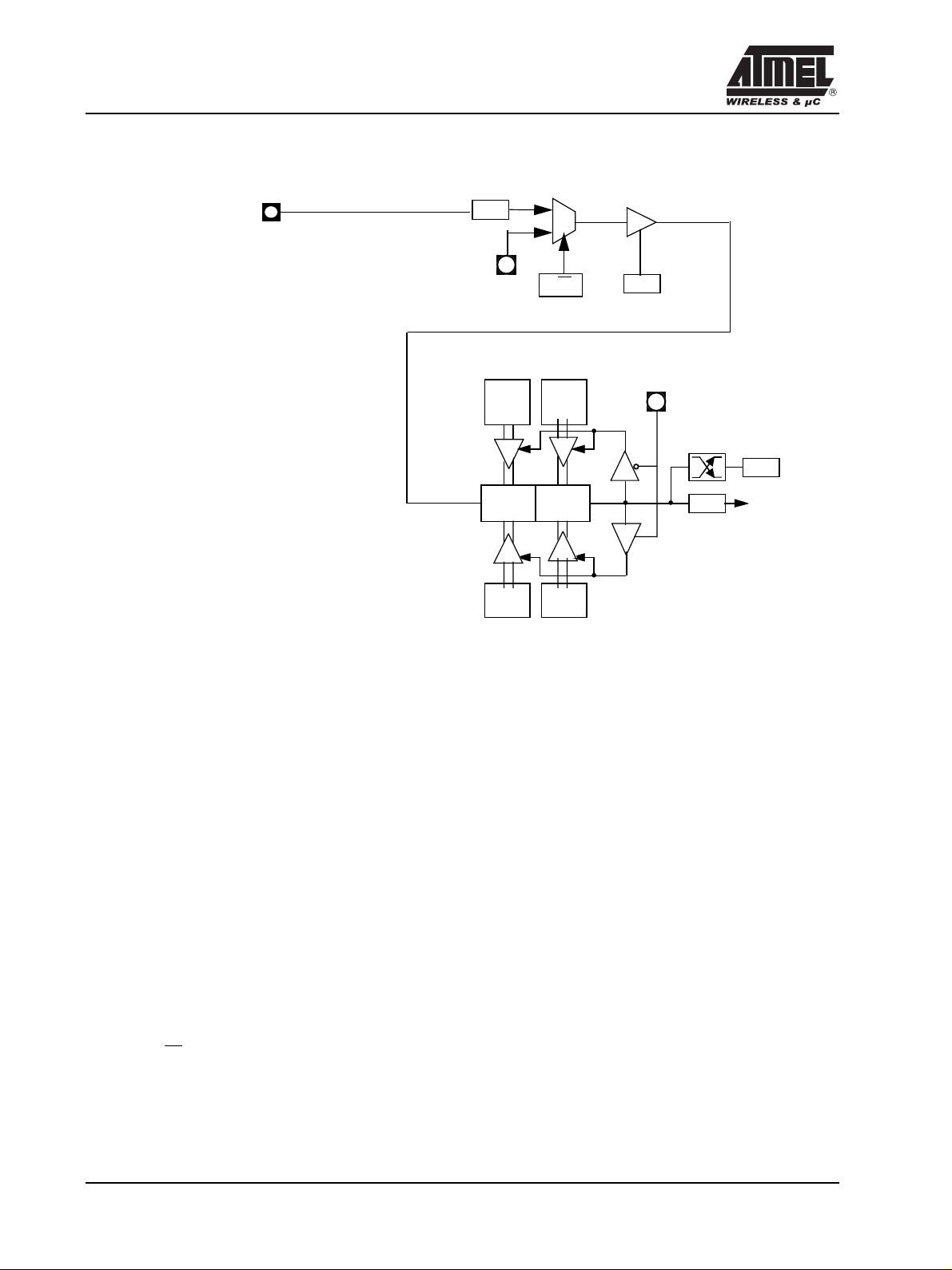
3. Block Diagram
CC
Vss
IB-bus
V
Flash
64Kx8
Parallel I/O Ports & Ext. Bus
Port 1
Port 0
Port 2
XRAM
1Kx8
Port 3
EEPROM
2Kx8
PCA
ECI
(1)
PCA
Port 5Port 4
(2)(2)
(1)
Watch
Dog
T2EX
(1) (1)
Timer2
ALE/
XTAL1
XTAL2
PROG
PSEN
EA
RD
WR
(3)
(3)
CPU
RxD
(3)(3)
EUART
Timer 0
Timer 1
TxD
C51
CORE
RAM
256x8
INT
Ctrl
I/O
T2
(3) (3) (3) (3)
P1
P2
RESET
T0
T1
INT1
INT0
(1): Alternate function of Port 1
(2): Only available on high pin count packages
(3): Alternate function of Port 3
P0
P3
P5
P4
2 Rev. F - 15 February, 2001
Page 3

T89C51RD2
4. SFR Mapping
The Special Function Registers (SFRs) of the T89C51RD2 fall into the following categories:
• C51 core registers: ACC, B, DPH, DPL, PSW, SP, AUXR1
• I/O port registers: P0, P1, P2, P3, P4, P5
• Timer registers: T2CON, T2MOD, TCON, TH0, TH1, TH2, TMOD, TL0, TL1, TL2, RCAP2L, RCAP2H
• Serial I/O port registers: SADDR, SADEN, SBUF, SCON
• Power and clock control registers: PCON
• Hardware Watchdog Timer register: WDTRST, WDTPRG
• Interrupt system registers: IE, IP, IPH
• Flash and EEPROM registers: FCON, EECON, EETIM
• Others: AUXR, AUXR1, CKCON
Table below shows all SFRs with their address and their reset value.
Bit
address-
able
0/8 1/9 2/A 3/B 4/C 5/D 6/E 7/F
F8h
F0h
E8h
E0h
D8h
D0h
C8h
C0h
B8h
B0h
A8h
A0h
98h
90h
88h
80h
B
0000 0000
P5
1111 1111CL0000 0000
ACC
0000 0000
CCON
00X0 0000
PSW
0000 0000
T2CON
0000 0000
P4
1111 1111
IP
X000 000
P3
1111 1111
IE
0000 0000
P2
1111 1111
SCON
0000 0000
P1
1111 1111
TCON
0000 0000
P0
1111 1111SP0000 0111
0/8 1/9 2/A 3/B 4/C 5/D 6/E 7/F
CH
0000 0000
CMOD
00XX X000
FCON
XXXX 0000
T2MOD
XXXX XX00
SADEN
0000 0000
SADDR
0000 0000
SBUF
XXXX XXXX
TMOD
0000 0000
CCAP0H
XXXX XXXX
CCAP0L
XXXX XXXX
CCAPM0
X000 0000
EECON
XXXX XX00
RCAP2L
0000 0000
AUXR1
XXXX 00X0
TL0
0000 0000
DPL
0000 0000
XXXX XXXX
XXXX XXXX
Non Bit addressable
CCAP1H
XXXX XXXX
CCAP1L
XXXX XXXX
CCAPM1
X000 0000
EETIM
0000 0000
RCAP2H
0000 0000
TL1
0000 0000
DPH
0000 0000
CCAPL2H
CCAPL2L
CCAPM2
X000 0000
TL2
0000 0000
TH0
0000 0000
CCAPL3H
XXXX XXXX
CCAPL3L
XXXX XXXX
CCAPM3
X000 0000
TH2
0000 0000
TH1
0000 0000
CCAPL4H
XXXX XXXX
CCAPL4L
XXXX XXXX
CCAPM4
X000 0000
WDTRST
XXXX XXXX
AUXR
XX0X 1000
P5
1111 1111
IPH
X000 0000
WDTPRG
XXXX X000
CKCON
X000 0000
PCON
00X1 0000
FFh
F7h
EFh
E7h
DFh
D7h
CFh
C7h
BFh
B7h
AFh
A7h
9Fh
97h
8Fh
87h
Rev. F - 15 February, 2001 3
Page 4

T89C51RD2
reserved
4 Rev. F - 15 February, 2001
Page 5
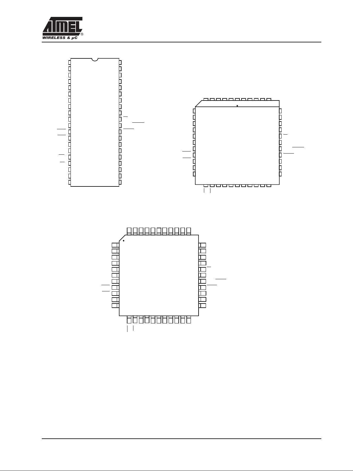
5. Pin Configuration
T89C51RD2
P1.0/T2
P1.1/T2EX
P1.2/ECI
P1.3CEX0
P1.4/CEX1
P1.5/CEX2
P1.6/CEX3
P1.7CEX4
RST
P3.0/RxD
P3.1/TxD
P3.2/INT0
P3.3/INT1
P3.4/T0
P3.5/T1
P3.6/WR
P3.7/RD
XTAL2
XTAL1
VSS
1
3
4
5
9
10
11
14
15
16
17
40
VCC
39
2
6
7
8
PDIL
12
13
18
19
20
38
37
36
35
34
33
32
31
30
29
28
27
26
25
24
23
22
21
P0.0/AD0
P0.1/AD1
P0.2/AD2
P0.3/AD3
P0.4/AD4
P0.5/AD5
P0.6/AD6
P0.7/AD7
EA
ALE/PROG
PSEN
P2.7/AD15
P2.6/AD14
P2.5/AD13
P2.4/AD12
P2.3/AD11
P2.2/AD10
P2.1/AD9
P2.0/AD8
P1.4/CEX1
P1.3/CEX0
P1.1/T2EX
P1.2/ECI
P1.0/T2
VSS1/NIC*
P1.5/CEX2
P1.6/CEX3
P1.7/CEx4
P3.0/RxD
P3.1/TxD
P3.2/INT0
P3.3/INT1
P3.4/T0
P3.5/T1
VCC
P0.0/AD0
RST
NIC*
P0.2/AD2
P0.3/AD3
P0.1/AD1
P1.4/CEX1
P1.3/CEX0
5 4 3 2 1 6
7
8
9
10
11
12
13
14
15
16
17
18 19 23222120 262524 27 28
P3.7/RD
P3.6/WR
P1.1/T2EX
P1.2/ECI
PLCC
XTAL2
XTAL1
P1.0/T2
VSS1/NIC*
VCC
44 43 42 41 40
NIC*
VSS
P2.0/A8
P0.0/AD0
P2.1/A9
P0.3/AD3
P0.2/AD2
P0.1/AD1
37
36
35
31
30
29
P2.2/A10
P2.3/A11
P2.4/A12
39
38
34
33
32
P0.4/AD4
P0.5/AD5
P0.6/AD6
P0.7/AD7
EA
NIC*
ALE/PROG
PSEN
P2.7/A15
P2.6/A14
P2.5/A13
P1.5/CEX2
P1.6/CEX3
P1.7/CEX4
P3.0/RxD
P3.1/TxD
P3.2/INT0
P3.3/INT1
*NIC: No Internal Connection
RST
NIC*
P3.4/T0
P3.5/T1
43 42 41 40 3944
1
2
3
4
5
6
7
8
9
10
11
12 13 17161514 201918 21 22
XTAL2
P3.7/RD
P3.6/WR
38 37 36 35 34
VQFP44 1.4
VSS
NIC*
XTAL1
P2.0/A8
P2.1/A9
P2.2/A10
33
32
31
30
29
28
27
26
25
24
23
P2.3/A11
P2.4/A12
P0.4/AD4
P0.5/AD5
P0.6/AD6
P0.7/AD7
EA
NIC*
ALE/PROG
PSEN
P2.7/A15
P2.6/A14
P2.5/A13
Rev. F - 15 February, 2001 5
Page 6
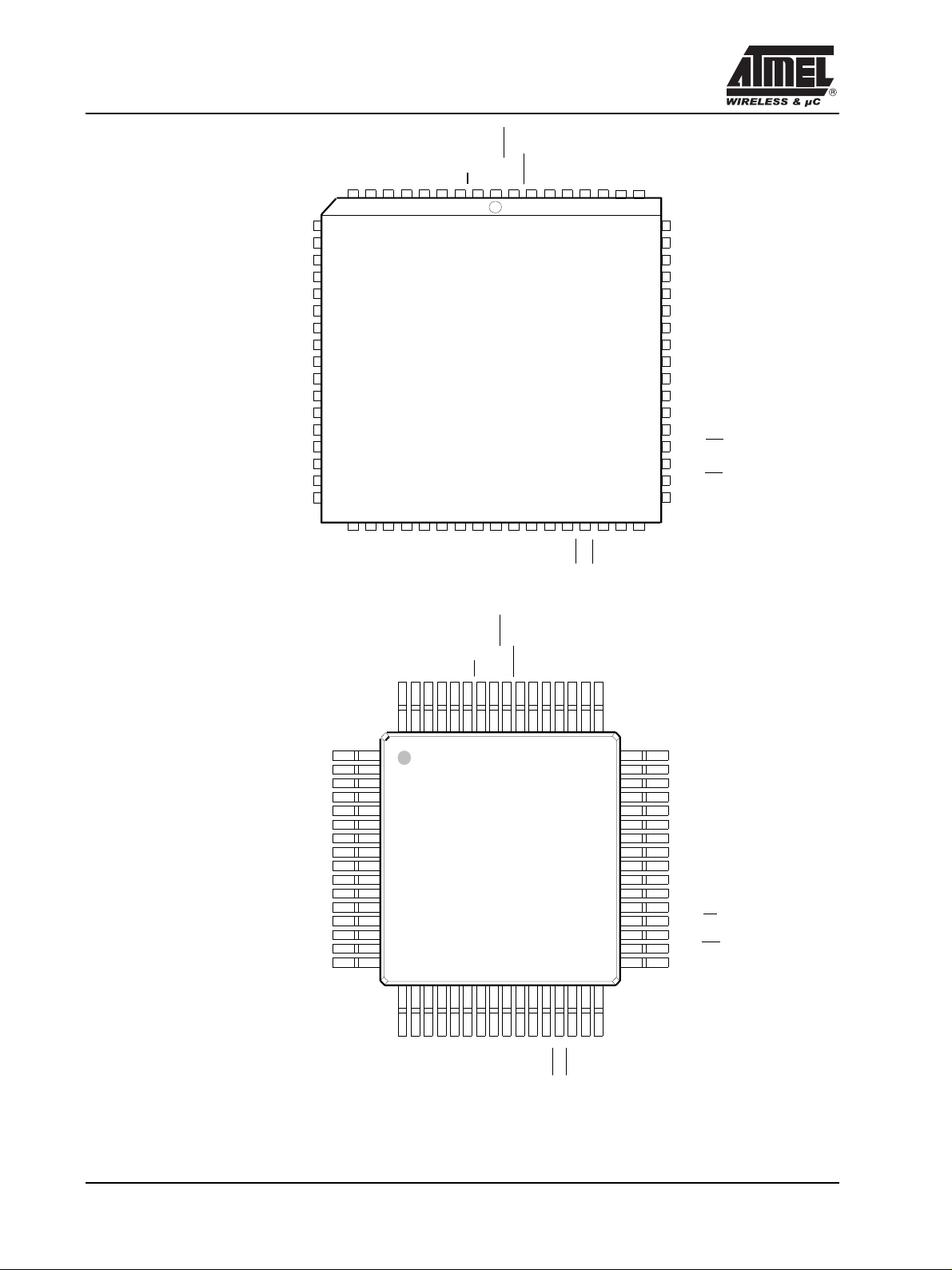
T89C51RD2
G
P0.3/AD3
P0.2/AD2
P0.1/AD1
P0.0/AD0
VSS1
P1.0/T2
P1.1/T2EX
P1.2/ECI
P1.3/CEX0
P1.4/CEX1
P5.5
P5.6
P5.7
VCC
P4.0
P4.1
P4.2
10
11
12
13
14
15
16
17
18
19
20
21
22
23
24
25
26
P0.4/AD4
89
27 28
P5.4
NIC
P0.5/AD5
P0.6/AD6
P5.3
29 30 313233
ALE/PRO
NIC
PSEN
NIC
EA
P0.7/AD7
23567 4 1 686766656463
PLCC 68
36 37 38 39 40 41
34 35
P2.7/A15
P2.6/A14
P5.2
62 61
42 43
P5.1
P2.5/A13
60
59
58
57
56
55
54
53
52
51
50
49
48
4647P4.4
45
44
P5.0
P2.4/A12
P2.3/A11
P4.7
P2.2/A10
P2.1/A9
P2.0/A8
P4.6
NIC
VSS
P4.5
XTAL1
XTAL2
P3.7/RD
P3.6/WR
P4.3
P5.5
P0.3/AD3
P0.2/AD2
P5.6
P0.1/AD1
P0.0/AD0
P5.7
VCC
VSS1
P1.0/T2
P4.0
P1.1/T2EX
P1.2/EC1
P1.3/CEX0
P4.1
P1.4/CEX1
P1.5/CEX2
P1.6/CEX3
P1.7/CEX4
1
2
3
4
5
6
7
8
9
10
11
12
13
14
15
16
NIC
RST
P0.4/AD4
P5.4
P5.3
NIC
NIC
NIC
NIC
P3.0/RxD
ALE/PROG
PSEN
EA
P0.5/AD5
NIC
P0.6/AD6
P0.7/AD7
58 5051525354555657596061626364 49
VQFP64 1.4
2618 19 20 21 22 23 24 25 27 28 29 30 31 3217
NIC
NIC
P5.2
P2.7/A15
P2.6/A14
P3.1/TxD
P3.2/INT0
P5.1
P5.0
P2.5/A13
48
47
46
45
44
43
42
41
40
39
38
37
36
35
34
33
P3.4/T0
P3.3/INT1
P3.5/T1
P2.4/A12
P2.3/A11
P4.7
P2.2/A10
P2.1/A9
P2.0/A8
P4.6
NIC
VSS
P4.5
XTAL1
XTAL2
P3.7/RD
P4.4
P3.6/WR
P4.3
P4.2
P1.6/CEX3
P1.5/CEX2
NIC
NIC
RST
P1.7/CEX4
NIC
P3.0/RxD
NIC
NIC
P3.1/TxD
P3.4/T0
P3.5/T1
P3.2/INT0
P3.3/INT1
NIC: No InternalConnection
6 Rev. F - 15 February, 2001
Page 7

T89C51RD2
Mnemonic
V
SS
Vss1 1 39 I Optional Ground: Contact the Sales Office for ground connection.
V
CC
P0.0-P0.7 39-32 43-36 37-30 I/O Port 0: Port 0 is an open-drain, bidirectional I/O port. Port 0 pins that have 1s
P1.0-P1.7 1-8 2-9 40-44
P2.0-P2.7 21-28 24-31 18-25 I/O Port 2: Port 2 is an 8-bit bidirectional I/O port with internal pull-ups. Port 2
P3.0-P3.7 10-17 11,
Pin Number
DIL LCC VQFP 1.4
20 22 16 I Ground: 0V reference
40 44 38 I
1-3
1 2 40 I/O T2 (P1.0): Timer/Counter 2 external count input/Clockout
2 3 41 I T2EX (P1.1): Timer/Counter 2 Reload/Capture/Direction Control
3 4 42 I ECI (P1.2): External Clock for the PCA
4 5 43 I/O CEX0 (P1.3): Capture/Compare External I/O for PCA module 0
5 6 44 I/O CEX1 (P1.4): Capture/Compare External I/O for PCA module 1
6 7 1 I/O CEX2 (P1.5): Capture/Compare External I/O for PCA module 2
7 8 2 I/O CEX3 (P1.6): Capture/Compare External I/O for PCA module 3
8 9 3 I/O CEX4 (P1.7): Capture/Compare External I/O for PCA module 4
5,
13-19
10 11 5 I RXD (P3.0): Serial input port
11 13 7 O TXD (P3.1): Serial output port
12 14 8 I INT0 (P3.2): External interrupt 0
13 15 9 I INT1 (P3.3): External interrupt 1
14 16 10 I T0 (P3.4): Timer 0 external input
15 17 11 I T1 (P3.5): Timer 1 external input
16 18 12 O WR (P3.6): External data memory write strobe
7-13
Type
Power Supply: This is the power supply voltage for normal, idle and powerdown operation
written to them float and can be used as high impedance inputs. Port 0 must be
polarized to VCCor VSSin order to prevent any parasitic current consumption.
Port 0 is also the multiplexed low-order address and data bus during access to
external program and data memory. In this application, it uses strong internal
pull-up when emitting 1s. Port 0 also inputs the code bytes during EPROM
programming. External pull-ups are required during program verification during
which P0 outputs the code bytes.
I/O Port 1: Port 1 is an 8-bit bidirectional I/O port with internal pull-ups. Port 1 pins
that have 1s written to them are pulled high by the internal pull-ups and can be
used as inputs. As inputs, Port 1 pins that are externally pulled low will source
current because of the internal pull-ups. Port 1 also receives the low-order address
byte during memory programming and verification.
Alternate functions for TSC8x54/58 Port 1 include:
pins that have 1s written to them are pulled high by the internal pull-ups and
can be used as inputs. As inputs, Port 2 pins that are externally pulled low will
source current because of the internal pull-ups. Port 2 emits the high-order address
byte during fetches from external program memory and during accesses to external
data memory that use 16-bit addresses (MOVX @DPTR).In this application, it
uses strong internal pull-ups emitting 1s. During accesses to external data memory
that use 8-bit addresses (MOVX @Ri), port 2 emits the contents of the P2 SFR.
Some Port 2 pins receive the high order address bits during EPROM programming
and verification:
P2.0 to P2.5 for RB devices
P2.0 to P2.6 for RC devices
P2.0 to P2.7 for RD devices.
I/O Port 3: Port 3 is an 8-bit bidirectional I/O port with internal pull-ups. Port 3 pins
that have 1s written to them are pulled high by the internal pull-ups and can be
used as inputs. As inputs, Port 3 pins that are externally pulled low will source
current because of the internal pull-ups. Port 3 also serves the special features
of the 80C51 family, as listed below.
Name and Function
Rev. F - 15 February, 2001 7
Page 8
T89C51RD2
Mnemonic
Reset 9 10 4 I/O Reset: A high on this pin for two machine cycles while the oscillator is running,
ALE/PROG 30 33 27 O (I) Address Latch Enable/Program Pulse: Output pulse for latching the low byte
PSEN 29 32 26 O Program Store ENable: The read strobe to external program memory. When
EA 31 35 29 I External Access Enable: EA must be externally held low to enable the device
XTAL1 19 21 15 I
XTAL2 18 20 14 O Crystal 2: Output from the inverting oscillator amplifier
Pin Number
DIL LCC VQFP 1.4
17 19 13 O RD (P3.7): External data memory read strobe
Type
resets the device. An internal diffused resistor to VSSpermits a power-on reset
using only an external capacitor to VCC. This pin is an output when the hardware
watchdog forces a system reset.
of the address during an access to external memory. In normal operation, ALE
is emitted at a constant rate of 1/6 (1/3 in X2 mode) the oscillator frequency,
and can be used for external timing or clocking. Note that one ALE pulse is
skipped during each access to external data memory. This pin is also the program
pulse input (PROG) during Flash programming. ALE can be disabled by setting
SFR’s AUXR.0 bit. With this bit set, ALE will be inactive during internal fetches.
executing code from the external program memory, PSEN is activated twice each
machine cycle, except that two PSEN activations are skipped during each access
to external data memory. PSEN is not activated during fetches from internal
program memory.
to fetch code from external program memory locations 0000H to FFFFH (RD).
If security level 1 is programmed, EA will be internally latched on Reset.
Crystal 1: Input to the inverting oscillator amplifier and input to the internal
clock generator circuits.
Name and Function
8 Rev. F - 15 February, 2001
Page 9
T89C51RD2
5.1. Pin Description for 64/68 pin Packages
Port 4 and Port 5 are 8-bit bidirectional I/O ports with internal pull-ups. Pins that have 1 written to them are pulled
high by the internal pull ups and can be used as inputs.
As inputs, pins that are externally pulled low will source current because of the internal pull-ups.
Refer to the previous pin description for other pins.
PLCC68
VSS 51, 18 9/40
VCC 17 8
P0.0 15 6
P0.1 14 5
P0.2 12 3
P0.3 11 2
P0.4 9 64
P0.5 6 61
P0.6 5 60
P0.7 3 59
P1.0 19 10
P1.1 21 12
P1.2 22 13
P1.3 23 14
P1.4 25 16
P1.5 27 18
P1.6 28 19
P1.7 29 20
P2.0 54 43
P2.1 55 44
P2.2 56 45
P2.3 58 47
P2.4 59 48
P2.5 61 50
P2.6 64 53
P2.7 65 54
P3.0 34 25
P3.1 39 28
P3.2 40 29
P3.3 41 30
P3.4 42 31
P3.5 43 32
P3.6 45 34
P3.7 47 36
RESET 30 21
ALE/PROG 68 56
PSEN 67 55
EA 2 58
XTAL1 49 38
XTAL2 48 37
P4.0 20 11
P4.1 24 15
P4.2 26 17
P4.3 44 33
P4.4 46 35
P4.5 50 39
P4.6 53 42
P4.7 57 46
P5.0 60 49
P5.1 62 51
P5.2 63 52
P5.3 7 62
P5.4 8 63
P5.5 10 1
P5.6 13 4
P5.7 16 7
SQUARE
VQFP64 1.4
Rev. F - 15 February, 2001 9
Page 10
T89C51RD2
6. Enhanced Features
In comparison to the original 80C52, the T89C51RD2 implements some new features, which are:
• The X2 option.
• The Dual Data Pointer.
• The extended RAM.
• The Programmable Counter Array (PCA).
• The Watchdog.
• The 4 level interrupt priority system.
• The power-off flag.
• The ONCE mode.
• The ALE disabling.
• Some enhanced features are also located in the UART and the timer 2.
6.1. X2 Feature and Clock Generation
The T89C51RD2 core needs only 6 clock periods per machine cycle. This feature called ”X2” provides the following
advantages:
• Divide frequency crystals by 2 (cheaper crystals) while keeping same CPU power.
• Save power consumption while keeping same CPU power (oscillator power saving).
• Save power consumption by dividing dynamically operating frequency by 2 in operating and idle modes.
• Increase CPU power by 2 while keeping same crystal frequency.
In order to keep the original C51 compatibility, a divider by 2 is inserted between the XTAL1 signal and the main
clock input of the core (phase generator). This divider may be disabled by software.
6.1.1. Description
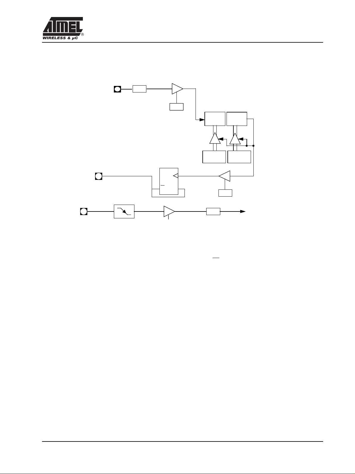
The clock for the whole circuit and peripheral is first divided by two before being used by the CPU core and
peripherals. This allows any cyclic ratio to be accepted on XTAL1 input. In X2 mode, as this divider is bypassed,
the signals on XTAL1 must have a cyclic ratio between 40 to 60%. Figure 1. shows the clock generation block
diagram. X2 bit is validated on XTAL1÷2 rising edge to avoid glitches when switching from X2 to STD mode.
Figure 2. shows the mode switching waveforms.
XTAL1:2
XTAL1
F
XTAL
2
0
1
X2
CKCON reg
F
OSC
state machine: 6 clock cycles.
CPU control
Figure 1. Clock Generation Diagram
Rev. F - 15 February, 2001 10
Page 11
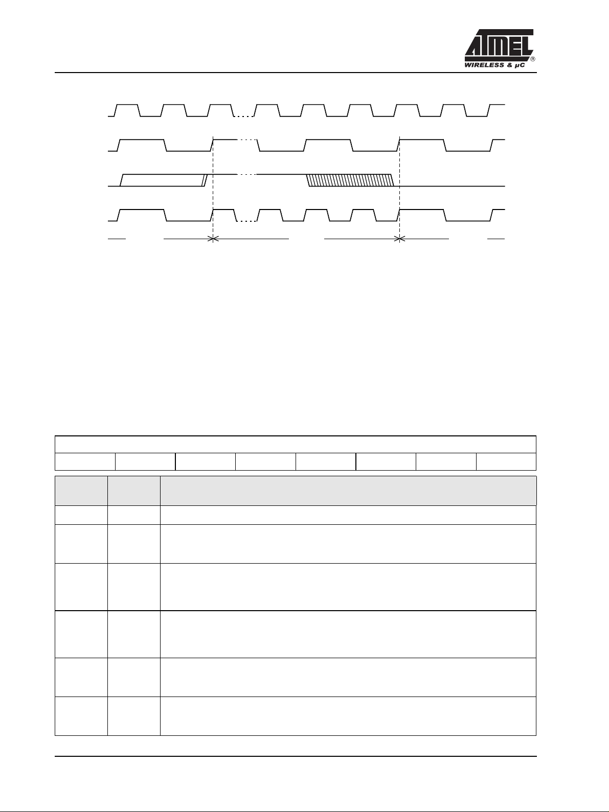
T89C51RD2
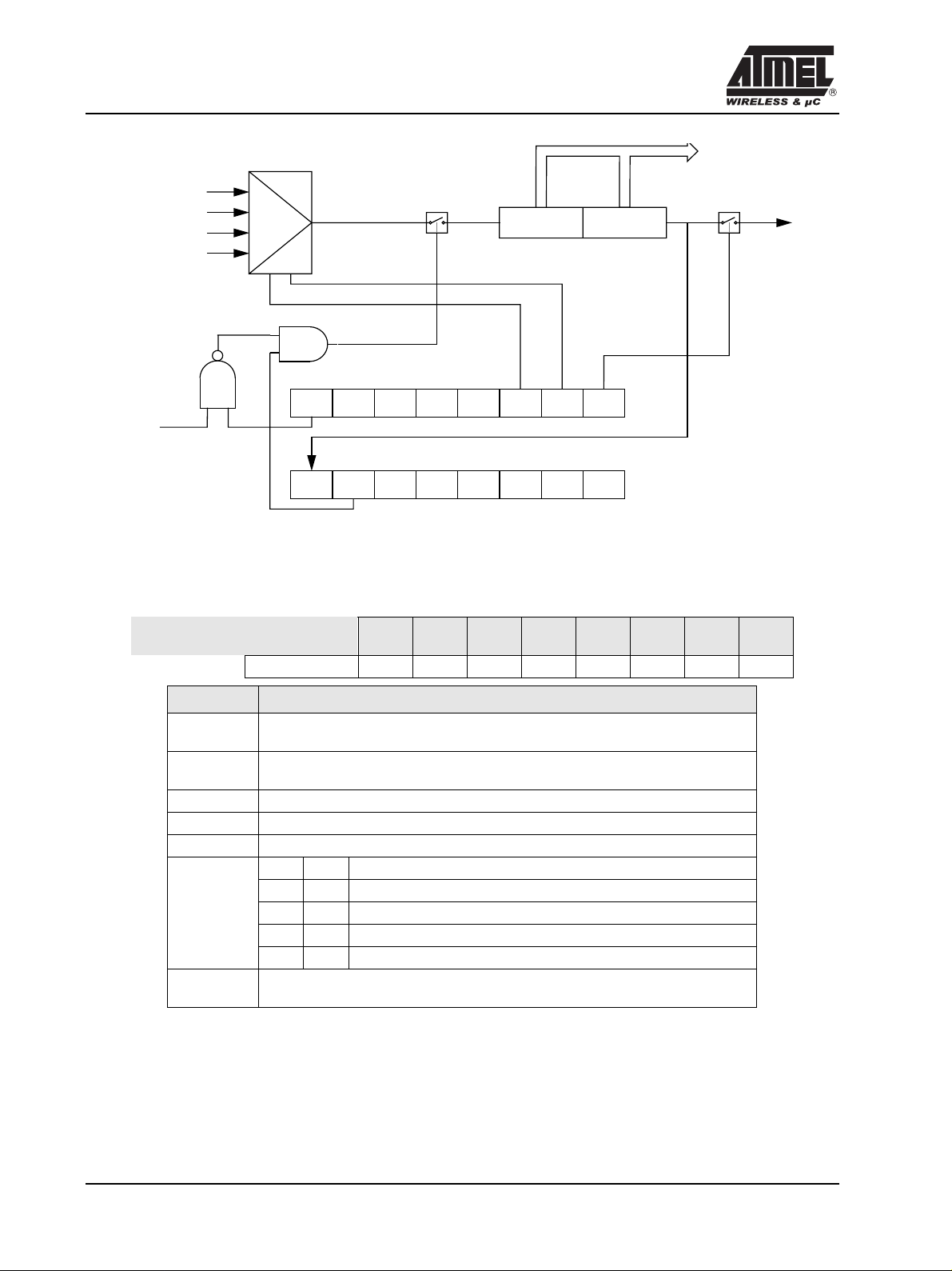
XTAL1
XTAL1:2
X2 bit
CPU clock
X2 ModeSTD Mode STD Mode
Figure 2. Mode Switching Waveforms
The X2 bit in the CKCON register (See Table 2.) allows to switch from 12 clock periods per instruction to 6
clock periods and vice versa. At reset, the standard speed is activated (STD mode). Setting this bit activates the
X2 feature (X2 mode).
The T0X2, T1X2, T2X2, SiX2, PcaX2 and WdX2 bits in the CKCON register (See Table 2.) allow to switch from
standard peripheral speed (12 clock periods per peripheral clock cycle) to fast peripheral speed (6 clock periods
per peripheral clock cycle). These bits are active only in X2 mode.
More information about the X2 mode can be found in the application note ANM072 "How to take advantage of
the X2 features in TS80C51 microcontroller?"
Table 2. CKCON Register
CKCON - Clock Control Register (8Fh)
7 6 5 4 3 2 1 0
- WdX2 PcaX2 SiX2 T2X2 T1X2 T0X2 X2
Bit
Number
7 - Reserved
6 WdX2
5 PcaX2
4 SiX2
Bit
Mnemonic
Description
Watchdogclock(Thiscontrol bit is validated when the CPU clock X2 is set; when X2 is low,this bit has no effect)
Clear to select 6 clock periods per peripheral clock cycle.
Set to select 12 clock periods per peripheral clock cycle.
Programmable Counter Array clock (This control bit is validated when the CPU clock X2 is set; when X2 is
low, this bit has no effect)
Clear to select 6 clock periods per peripheral clock cycle.
Set to select 12 clock periods per peripheral clock cycle.
Enhanced UART clock (Mode 0 and 2) (This control bit is validated when the CPU clock X2 is set; when X2
is low, this bit has no effect)
Clear to select 6 clock periods per peripheral clock cycle.
Set to select 12 clock periods per peripheral clock cycle.
Timer2 clock (This control bit is validated when the CPU clock X2 is set; when X2 is low, this bit has no effect)
3 T2X2
2 T1X2
Clear to select 6 clock periods per peripheral clock cycle.
Set to select 12 clock periods per peripheral clock cycle.
Timer1 clock (This control bit is validated when the CPU clock X2 is set; when X2 is low, this bit has no effect)
Clear to select 6 clock periods per peripheral clock cycle.
Set to select 12 clock periods per peripheral clock cycle
11 Rev. F - 15 February, 2001
Page 12

T89C51RD2
Bit
Number
1 T0X2
0 X2
Bit
Mnemonic
Reset Value = X000 0000b
Not bit addressable
Description
Timer0 clock (This control bit is validated when the CPU clock X2 is set; when X2 is low, this bit has no effect)
Clear to select 6 clock periods per peripheral clock cycle.
Set to select 12 clock periods per peripheral clock cycle
CPU clock
Clear to select 12 clock periods per machine cycle (STD mode) for CPU and all the peripherals.
Set to select 6clock periods per machine cycle (X2 mode) and to enable the individual peripherals "X2" bits.
Rev. F - 15 February, 2001 12
Page 13
T89C51RD2
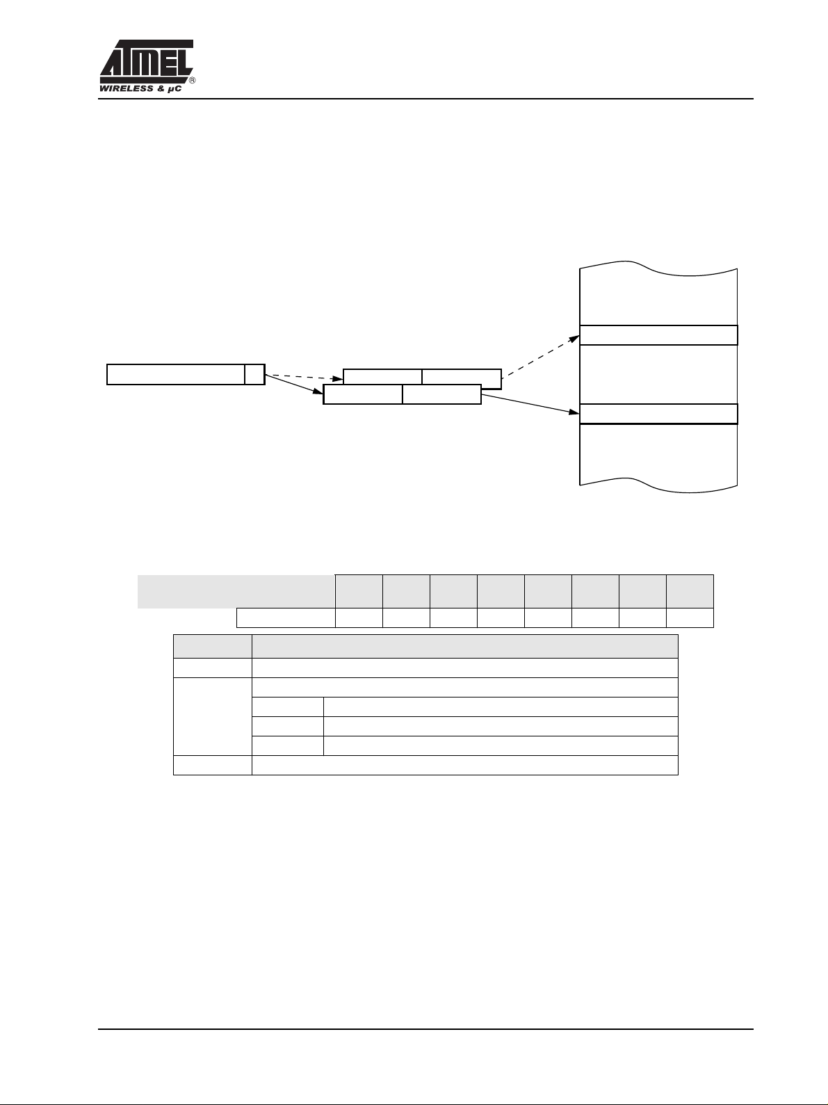
6.2. Dual Data Pointer Register Ddptr
The additional data pointer can be used to speed up code execution and reduce code size.
The dual DPTR structure is a way by which the chip will specify the address of an external data memory location.
There are two 16-bit DPTR registers that address the external memory, and a single bit called
DPS = AUXR1/bit0 (See Table 3.) that allows the program code to switch between them (Refer to Figure 3).
External Data Memory
07
DPS
AUXR1(A2H)
DPH(83H) DPL(82H)
DPTR1
DPTR0
AUXR1
Address 0A2H
a. User software should not write 1s to reserved bits. These bits may be used in future 8051 family
b. Bit 2 stuck at 0; this allows to use INC AUXR1 to toggle DPS without changing GF3.
Application
Figure 3. Use of Dual Pointer
Table 3. AUXR1: Auxiliary Register 1
- - - - GF3 0 - DPS
Reset value X X X X 0 0 X 0
Symbol
- Not implemented, reserved for future use.
DPS Data Pointer Selection.
GF3 This bit is a general purpose user flag
products to invoke new feature. In that case, the reset value of the new bit will be 0, and its active
value will be 1. The value read from a reserved bit is indeterminate.
Function
DPS Operating Mode
0 DPTR0 Selected
1 DPTR1 Selected
a
b
.
Software can take advantage of the additional data pointers to both increase speed and reduce code size, for
example, block operations (copy, compare, search ...) are well served by using one data pointer as a ’source’
pointer and the other one as a "destination" pointer.
ASSEMBLY LANGUAGE
Rev. F - 15 February, 2001 13
Page 14

T89C51RD2
; Block move using dual data pointers
; Modifies DPTR0, DPTR1, A and PSW
; note: DPS exits opposite of entry state
; unless an extra INC AUXR1 is added
;
00A2 AUXR1 EQU 0A2H
;
0000 909000MOV DPTR,#SOURCE ; address of SOURCE
0003 05A2 INC AUXR1 ; switch data pointers
0005 90A000 MOV DPTR,#DEST ; address of DEST
0008 LOOP:
0008 05A2 INC AUXR1 ; switch data pointers
000A E0 MOVX A,@DPTR ; get a byte from SOURCE
000B A3 INC DPTR ; increment SOURCE address
000C 05A2 INC AUXR1 ; switch data pointers
000E F0 MOVX @DPTR,A ; write the byte to DEST
000F A3 INC DPTR ; increment DEST address
0010 70F6JNZ LOOP ; check for 0 terminator
0012 05A2 INC AUXR1 ; (optional) restore DPS
INC is a short (2 bytes) and fast (12 clocks) way to manipulate the DPS bit in the AUXR1 SFR. However, note
that the INC instruction does not directly force the DPS bit to a particular state, but simply toggles it. In simple
routines, such as the block move example, only the fact that DPS is toggled in the proper sequence matters, not
its actual value. In other words, the block move routine works the same whether DPS is '0' or '1' on entry. Observe
that without the last instruction (INC AUXR1), the routine will exit with DPS in the opposite state.
14 Rev. F - 15 February, 2001
Page 15
T89C51RD2
6.3. Expanded RAM (XRAM)
The T89C51RD2 provide additional Bytes of random access memory (RAM) space for increased data parameter
handling and high level language usage.
T89C51RD2 devices have expanded RAM in external data space; Maximum size and location are described in Table 4.
Table 4. Description of expanded RAM
Port XRAM size
T89C51RD2 1024 00h 3FFh
Start End
The T89C51RD2 has internal data memory that is mapped into four separate segments.
The four segments are:
• 1. The Lower 128 bytes of RAM (addresses 00H to 7FH) are directly and indirectly addressable.
• 2. The Upper 128 bytes of RAM (addresses 80H to FFH) are indirectly addressable only.
• 3. The Special Function Registers, SFRs, (addresses 80H to FFH) are directly addressable only.
• 4. The expanded RAM bytes are indirectly accessed by MOVX instructions, and with the EXTRAM bit
cleared in the AUXR register. (See )
The Lower 128 bytes can be accessed by either direct or indirect addressing. The Upper 128 bytes can be accessed
by indirect addressing only. The Upper 128 bytes occupy the same address space as the SFR. That means they
have the same address, but are physically separate from SFR space.
Address
FF or 3FF
XRAM
00
FF
Upper
128 bytes
Internal
Ram
indirect accesses
80 80
Lower
128 bytes
Internal
Ram
direct or indirect
00
accesses
FF
Special
Function
Register
direct accesses
FFFF
0100 or 0400
0000
External
Data
Memory
Figure 4. Internal and External Data Memory Address
When an instruction accesses an internal location above address 7FH, the CPU knows whether the access is to the
upper 128 bytes of data RAM or to SFR space by the addressing mode used in the instruction.
• Instructions that use direct addressing access SFR space. For example: MOV 0A0H, # data ,accesses the SFR
at location 0A0H (which is P2).
• Instructions that use indirect addressing access the Upper 128 bytes of data RAM. For example: MOV @R0,
# data where R0 contains 0A0H, accesses the data byte at address 0A0H, rather than P2 (whose address is 0A0H).
Rev. F - 15 February, 2001 15
Page 16
T89C51RD2
• The XRAM bytes can be accessed by indirect addressing, with EXTRAM bit cleared and MOVX instructions.
This part of memory which is physically located on-chip, logically occupies the first bytes of external data
memory. The bits XRS0 and XRS1 are used to hide a part of the available XRAM as explained in Table . This
can be useful if external peripherals are mapped at addresses already used by the internal XRAM.
• With EXTRAM = 0, the XRAM is indirectly addressed, using the MOVX instruction in combination with any
of the registers R0, R1 of the selected bank or DPTR. An access to XRAM will not affect ports P0, P2, P3.6
(WR) and P3.7 (RD). For example, with EXTRAM = 0, MOVX @R0, # data where R0 contains 0A0H,
accesses the XRAM at address 0A0H rather than external memory. An access to external data memory locations
higher than the accessible size of the XRAM will be performed with the MOVX DPTR instructions in the
same way as in the standard 80C51, so with P0 and P2 as data/address busses, and P3.6 and P3.7 as write and
read timing signals. Accesses to XRAM above 0FFH can only be done thanks to the use of DPTR.
• With EXTRAM = 1, MOVX @Ri and MOVX @DPTR will be similar to the standard 80C51. MOVX @ Ri
will provide an eight-bit address multiplexed with data on Port0 and any output port pins can be used to output
higher order address bits. This is to provide the external paging capability. MOVX @DPTR will generate a
sixteen-bit address. Port2 outputs the high-order eight address bits (the contents of DPH) while Port0 multiplexes
the low-order eight address bits (DPL) with data. MOVX @ Ri and MOVX @DPTR will generate either read
or write signals on P3.6 (WR) and P3.7 (RD).
The stack pointer (SP) may be located anywhere in the 256 bytes RAM (lower and upper RAM) internal data
memory. The stack may not be located in the XRAM.
The M0 bit allows to stretch the XRAM timings; if M0 is set, the read and write pulses are extended from 6 to
30 clock periods. This is useful to access external slow peripherals.
Auxiliary Register AUXR
AUXR
Address 08EH
Reset value X X 0 X 1 0 0 0
Symbol Function
- Not implemented, reserved for future use.
AO Disable/Enable ALE
AO Operating Mode
0 ALE is emitted at a constant rate of 1/6 the oscillator frequency (or 1/3 if X2 mode is used)
1 ALE is active only during a MOVX or MOVC instruction
EXTRAM Internal/External RAM (00H-FFH) access using MOVX @ Ri/ @ DPTR
EXTRAM Operating Mode
0 Internal XRAM access using MOVX @ Ri/ @ DPTR
1 External data memory access
XRS0
XRS1
M0 Stretch MOVX control: the RD/ and the WR/ pulse length is increased according to the value of M0
XRAM size: Accessible size of the XRAM
XRS1:0 XRAM size
00 256 bytes
01 512 bytes
10 768 bytes (default)
11 1024 bytes
M0 Pulse length in clock period
0 6
1 30
- - M0 - XRS1 XRS0 EXTRAM AO
a
a. User software should not write 1s to reserved bits. These bits may be used in future 8051 family products to invoke new features. In
that case, the reset or inactive value of the new bit will be 0, and its active value will be 1. The value read from a reserved bit is
indeterminate.
16 Rev. F - 15 February, 2001
Page 17

T89C51RD2
6.4. Timer 2
The timer 2 in the T89C51RD2 is compatible with the timer 2 in the 80C52.
It is a 16-bit timer/counter: the count is maintained by two eight-bit timer registers, TH2 and TL2, connected in
cascade. It is controlled by T2CON register (See Table 5) and T2MOD register (See Table 6). Timer 2 operation
is similar to Timer 0 and Timer 1. C/T2 selects F
as the timer clock input. Setting TR2 allows TL2 to be incremented by the selected input.
Timer 2 has 3 operating modes: capture, autoreload and Baud Rate Generator. These modes are selected by the
combination of RCLK, TCLK and CP/RL2 (T2CON), as described in the ATMEL Wireless and Micrcontrollers
8-bit Microcontroller Hardware description.
Refer to the ATMEL Wireless and Micrcontrollers 8-bit Microcontroller Hardware description for the description
of Capture and Baud Rate Generator Modes.
In T89C51RD2 Timer 2 includes the following enhancements:
• Auto-reload mode with up or down counter
• Programmable clock-output
6.4.1. Auto-Reload Mode
The auto-reload mode configures timer 2 as a 16-bit timer or event counter with automatic reload. If DCEN bit
in T2MOD is cleared, timer 2 behaves as in 80C52 (refer to the ATMEL Wireless and Micrcontrollers 8-bit
Microcontroller Hardware description). If DCEN bit is set, timer 2 acts as an Up/down timer/counter as shown in
Figure 5. In this mode the T2EX pin controls the direction of count.
/12 (timer operation) or external pin T2 (counter operation)
OSC
When T2EX is high, timer 2 counts up. Timer overflow occurs at FFFFh which sets the TF2 flag and generates
an interrupt request. The overflow also causes the 16-bit value in RCAP2H and RCAP2L registers to be loaded
into the timer registers TH2 and TL2.
When T2EX is low, timer 2 counts down. Timer underflow occurs when the count in the timer registers TH2 and
TL2 equals the value stored in RCAP2H and RCAP2L registers. The underflow sets TF2 flag and reloads FFFFh
into the timer registers.
The EXF2 bit toggles when timer 2 overflows or underflows according to the the direction of the count. EXF2
does not generate any interrupt. This bit can be used to provide 17-bit resolution.
Rev. F - 15 February, 2001 17
Page 18
T89C51RD2
XTAL1
F
XTAL
F
:12
OSC
T2
(DOWN COUNTING RELOAD VALUE)
FFh
(8-bit)
TL2
(8-bit)
RCAP2L
(8-bit)
(UP COUNTING RELOAD VALUE)
0
1
C/T2
T2CONreg
FFh
(8-bit)
TH2
(8-bit)
RCAP2H
(8-bit)
Figure 5. Auto-Reload Mode Up/Down Counter (DCEN = 1)
TR2
T2CONreg
T2EX:
if DCEN=1, 1=UP
if DCEN=1, 0=DOWN
if DCEN = 0, up counting
TOGGLE
TF2
T2CONreg
T2CONreg
EXF2
TIMER 2
INTERRUPT
6.4.2. Programmable Clock-Output
In the clock-out mode, timer 2 operates as a 50%-duty-cycle, programmable clock generator (See Figure 6) . The
input clock increments TL2 at frequency F
/2. The timer repeatedly counts to overflow from a loaded value.
OSC
At overflow, the contents of RCAP2H and RCAP2L registers are loaded into TH2 and TL2. In this mode, timer
2 overflows do not generate interrupts. The formula gives the clock-out frequency as a function of the system
oscillator frequency and the value in the RCAP2H and RCAP2L registers :
F
Clock OutFrequency–
--------------------------------------------------------------------------------------=
4 65536 RCAP2H– RCAP2L⁄()×
osc
For a 16 MHz system clock, timer 2 has a programmable frequency range of 61 Hz
OSC
16)
/2
to 4 MHz (F
/4). The generated clock signal is brought out to T2 pin (P1.0).
OSC
(F
Timer 2 is programmed for the clock-out mode as follows:
• Set T2OE bit in T2MOD register.
• Clear C/T2 bit in T2CON register.
• Determine the 16-bit reload value from the formula and enter it in RCAP2H/RCAP2L registers.
• Enter a 16-bit initial value in timer registers TH2/TL2. It can be the same as the reload value or a different
one depending on the application.
• To start the timer, set TR2 run control bit in T2CON register.
18 Rev. F - 15 February, 2001
Page 19
T89C51RD2
It is possible to use timer 2 as a baud rate generator and a clock generator simultaneously. For this configuration,
the baud rates and clock frequencies are not independent since both functions use the values in the RCAP2H and
RCAP2L registers.
T2EX
T2
XTAL1
:2
TR2
T2CON reg
Toggle
QD
EXEN2
T2CON reg
TL2
(8-bit)
RCAP2L
(8-bit)
T2OE
T2MOD reg
EXF2
T2CON reg
TH2
(8-bit)
RCAP2H
(8-bit)
OVEFLOW
TIMER 2
INTERRUPT
Figure 6. Clock-Out Mode C/T2=0
Rev. F - 15 February, 2001 19
Page 20

T89C51RD2
Table 5. T2CON Register
T2CON - Timer 2 Control Register (C8h)
7 6 5 4 3 2 1 0
TF2 EXF2 RCLK TCLK EXEN2 TR2 C/T2# CP/RL2#
Bit
Number
7 TF2
6 EXF2
5 RCLK
4 TCLK
3 EXEN2
2 TR2
1 C/T2#
Bit
Mnemonic
Description
Timer 2 overflow Flag
Must be cleared by software.
Set by hardware on timer 2 overflow, if RCLK = 0 and TCLK = 0.
Timer 2 External Flag
Set when a capture or a reload is caused by a negative transition on T2EX pin if EXEN2=1.
When set, causes the CPU to vector to timer 2 interrupt routine when timer 2 interrupt is enabled.
Must be cleared by software. EXF2 doesn’t cause an interrupt in Up/down counter mode (DCEN = 1)
Receive Clock bit
Clear to use timer 1 overflow as receive clock for serial port in mode 1 or 3.
Set to use timer 2 overflow as receive clock for serial port in mode 1 or 3.
Transmit Clock bit
Clear to use timer 1 overflow as transmit clock for serial port in mode 1 or 3.
Set to use timer 2 overflow as transmit clock for serial port in mode 1 or 3.
Timer 2 External Enable bit
Clear to ignore events on T2EX pin for timer 2 operation.
Set to cause a capture or reload when a negative transition on T2EX pin is detected, if timer 2 is not used to
clock the serial port.
Timer 2 Run control bit
Clear to turn off timer 2.
Set to turn on timer 2.
Timer/Counter 2 select bit
Clear for timer operation (input from internal clock system: F
Set for counter operation (input from T2 input pin, falling edge trigger). Must be 0 for clock out mode.
OSC
).
0 CP/RL2#
Reset Value = 0000 0000b
Bit addressable
Timer 2 Capture/Reload bit
If RCLK=1 or TCLK=1, CP/RL2# is ignored and timer is forced to auto-reload on timer 2 overflow.
Clear to auto-reload on timer 2 overflows or negative transitions on T2EX pin if EXEN2=1.
Set to capture on negative transitions on T2EX pin if EXEN2=1.
20 Rev. F - 15 February, 2001
Page 21

T89C51RD2
Table 6. T2MOD Register
T2MOD - Timer 2 Mode Control Register (C9h)
7 6 5 4 3 2 1 0
- - - - - - T2OE DCEN
Bit
Number
7 -
6 -
5 -
4 -
3 -
2 -
1 T2OE
0 DCEN
Bit
Mnemonic
Reserved
Reserved
Reserved
Reserved
Reserved
Reserved
Timer 2 Output Enable bit
Down Counter Enable bit
Reset Value = XXXX XX00b
Not bit addressable
Description
The value read from this bit is indeterminate. Do not set this bit.
The value read from this bit is indeterminate. Do not set this bit.
The value read from this bit is indeterminate. Do not set this bit.
The value read from this bit is indeterminate. Do not set this bit.
The value read from this bit is indeterminate. Do not set this bit.
The value read from this bit is indeterminate. Do not set this bit.
Clear to program P1.0/T2 as clock input or I/O port.
Set to program P1.0/T2 as clock output.
Clear to disable timer 2 as up/down counter.
Set to enable timer 2 as up/down counter.
Rev. F - 15 February, 2001 21
Page 22

T89C51RD2
6.5. Programmable Counter Array PCA
The PCA provides more timing capabilities with less CPU intervention than the standard timer/counters. Its
advantages include reduced software overhead and improved accuracy. The PCA consists of a dedicated timer/
counter which serves as the time base for an array of five compare/ capture modules. Its clock input can be
programmed to count any one of the following signals:
• Oscillator frequency ÷ 12 (÷ 6 in X2 mode)
• Oscillator frequency ÷ 4(÷ 2 in X2 mode)
• Timer 0 overflow
• External input on ECI (P1.2)
Each compare/capture modules can be programmed in any one of the following modes:
• rising and/or falling edge capture,
• software timer,
• high-speed output, or
• pulse width modulator.
Module 4 can also be programmed as a watchdog timer (See Section "PCA Watchdog Timer", page 31).
When the compare/capture modules are programmed in the capture mode, software timer, or high speed output
mode, an interrupt can be generated when the module executes its function. All five modules plus the PCA timer
overflow share one interrupt vector.
The PCA timer/counter and compare/capture modules share Port 1 for external I/O. These pins are listed below.
If the port is not used for the PCA, it can still be used for standard I/O.
PCA component External I/O Pin
16-bit Counter P1.2 / ECI
16-bit Module 0 P1.3 / CEX0
16-bit Module 1 P1.4 / CEX1
16-bit Module 2 P1.5 / CEX2
16-bit Module 3 P1.6 / CEX3
16-bit Module 4 P1.7 / CEX4
The PCA timer is a common time base for all five modules (See Figure 7). The timer count source is determined
from the CPS1 and CPS0 bits in the CMOD SFR (See Table 7) and can be programmed to run at:
• 1/12 the oscillator frequency. (Or 1/6 in X2 Mode)
• 1/4 the oscillator frequency. (Or 1/2 in X2 Mode)
• The Timer 0 overflow
• The input on the ECI pin (P1.2)
Rev. F - 15 February, 2001 22
Page 23
T89C51RD2
Fosc /12
Fosc / 4
T0 OVF
P1.2
CH CL
16 bit up/down counter
overflow
To PCA
modules
It
CIDL CPS1 CPS0 ECF
WDTE
Idle
CF CR
Figure 7. PCA Timer/Counter
Table 7. CMOD: PCA Counter Mode Register
CMOD
Address 0D9H
Reset value 0 0 X X X 0 0 0
Symbol
CIDL
WDTE
- Not implemented, reserved for future use.
CPS1 PCA Count Pulse Select bit 1.
CPS0 PCA Count Pulse Select bit 0.
ECF
Function
Counter Idle control: CIDL = 0 programs the PCA Counter to continue functioning during
idle Mode. CIDL = 1 programs it to be gated off during idle.
Watchdog Timer Enable: WDTE = 0 disables Watchdog Timer function on PCA Module 4.
WDTE = 1 enables it.
CPS1 CPS0 Selected PCA input.
0 0 Internal clock f
0 1 Internal clock f
1 0 Timer 0 Overflow
1 1 External clock at ECI/P1.2 pin (max rate = f
PCA Enable Counter Overflow interrupt: ECF = 1 enables CF bit in CCON to generate an
interrupt. ECF = 0 disables that function of CF.
CIDL WDTE - - - CPS1 CPS0 ECF
CCF4 CCF3 CCF2 CCF1 CCF0
a
b
/12 ( Or f
osc
/4 ( Or f
osc
/6 in X2 Mode).
osc
/2 in X2 Mode).
osc
osc
/8)
CMOD
0xD9
CCON
0xD8
a. User software should not write 1s to reserved bits. These bits may be used in future 8051 family
products to invoke new features. In that case, the reset or inactive value of the new bit will be 0, and its
active value will be 1. The value read from a reserved bit is indeterminate.
b. f
= oscillator frequency
osc
The CMOD SFR includes three additional bits associated with the PCA (See Figure 7 and Table 7).
• The CIDL bit which allows the PCA to stop during idle mode.
• The WDTE bit which enables or disables the watchdog function on module 4.
23 Rev. F - 15 February, 2001
Page 24
T89C51RD2
• The ECF bit which when set causes an interrupt and the PCA overflow flag CF (in the CCON SFR) to be set
when the PCA timer overflows.
The CCON SFR contains the run control bit for the PCA and the flags for the PCA timer (CF) and each module
(Refer to Table 8).
• Bit CR (CCON.6) must be set by software to run the PCA. The PCA is shut off by clearing this bit.
• Bit CF: The CF bit (CCON.7) is set when the PCA counter overflows and an interrupt will be generated if the
ECF bit in the CMOD register is set. The CF bit can only be cleared by software.
• Bits 0 through 4 are the flags for the modules (bit 0 for module 0, bit 1 for module 1, etc.) and are set by
hardware when either a match or a capture occurs. These flags also can only be cleared by software.
Table 8. CCON: PCA Counter Control Register
CCON
Address 0D8H
Reset value 0 0 X 0 0 0 0 0
Symbol
CF
CR
- Not implemented, reserved for future use.
CCF4
CCF3
CCF2
CCF1
CCF0
a. User software should not write 1s to reserved bits. These bits may be used in future 8051 family
products to invoke new features. In that case, the reset or inactive value of the new bit will be 0, and its
active value will be 1. The value read from a reserved bit is indeterminate.
Function
PCA Counter Overflow flag. Set by hardware when the counter rolls over. CF flags
an interrupt if bit ECF in CMOD is set. CF may be set by either hardware or software but
can only be cleared by software.
PCA Counter Run control bit. Set by software to turn the PCA counter on. Must be cleared
by software to turn the PCA counter off.
PCA Module 4 interrupt flag. Set by hardware when a match or capture occurs. Must be
cleared by software.
PCA Module 3 interrupt flag. Set by hardware when a match or capture occurs. Must be
cleared by software.
PCA Module 2 interrupt flag. Set by hardware when a match or capture occurs. Must be
cleared by software.
PCA Module 1 interrupt flag. Set by hardware when a match or capture occurs. Must be
cleared by software.
PCA Module 0 interrupt flag. Set by hardware when a match or capture occurs. Must be
cleared by software.
CF CR - CCF4 CCF3 CCF2 CCF1 CCF0
a
The watchdog timer function is implemented in module 4 (See Figure 10).
The PCA interrupt system is shown in Figure 8
Rev. F - 15 February, 2001 24
Page 25
T89C51RD2
CCON
0xD8
To Interrupt
priority decoder
PCA Timer/Counter
Module 0
Module 1
Module 2
Module 3
Module 4
ECF
CF CR
ECCFn
CCF4 CCF3 CCF2 CCF1 CCF0
CCAPMn.0CMOD.0
IE.6 IE.7
EC EA
Figure 8. PCA Interrupt System
PCA Modules: each one of the five compare/capture modules has six possible functions. It can perform:
• 16-bit Capture, positive-edge triggered,
• 16-bit Capture, negative-edge triggered,
• 16-bit Capture, both positive and negative-edge triggered,
• 16-bit Software Timer,
• 16-bit High Speed Output,
• 8-bit Pulse Width Modulator.
In addition, module 4 can be used as a Watchdog Timer.
Each module in the PCA has a special function register associated with it. These registers are: CCAPM0 for module
0, CCAPM1 for module 1, etc. (See Table 9). The registers contain the bits that control the mode that each module
will operate in.
• The ECCF bit (CCAPMn.0 where n=0, 1, 2, 3, or 4 depending on the module) enables the CCF flag in the
CCON SFR to generate an interrupt when a match or compare occurs in the associated module.
• PWM (CCAPMn.1) enables the pulse width modulation mode.
• The TOG bit (CCAPMn.2) when set causes the CEX output associated with the module to toggle when there
is a match between the PCA counter and the module's capture/compare register.
• The match bit MAT (CCAPMn.3) when set will cause the CCFn bit in the CCON register to be set when there
is a match between the PCA counter and the module's capture/compare register.
• The next two bits CAPN (CCAPMn.4) and CAPP (CCAPMn.5) determine the edge that a capture input will
be active on. The CAPN bit enables the negative edge, and the CAPP bit enables the positive edge. If both
bits are set both edges will be enabled and a capture will occur for either transition.
• The last bit in the register ECOM (CCAPMn.6) when set enables the comparator function.
Table 10 shows the CCAPMn settings for the various PCA functions.
.
25 Rev. F - 15 February, 2001
Page 26
Table 9. CCAPMn: PCA Modules Compare/Capture Control Registers
CCAPMn Address
n=0-4
T89C51RD2
CCAPM0=0DAH
CCAPM1=0DBH
CCAPM2=0DCH
CCAPM3=0DDH
CCAPM4=0DEH
- ECOMn CAPPn CAPNn MATn TOGn PWMm ECCFn
Reset value X 0 0 0 0 0 0 0
Symbol
- Not implemented, reserved for future use.
ECOMn Enable Comparator. ECOMn = 1 enables the comparator function.
CAPPn Capture Positive, CAPPn = 1 enables positive edge capture.
CAPNn Capture Negative, CAPNn = 1 enables negative edge capture.
MATn
TOGn
PWMn
ECCFn
a. User software should not write 1s to reserved bits. These bits may be used in future 8051 family
products to invoke new features. In that case, the reset or inactive value of the new bit will be 0, and its
active value will be 1. The value read from a reserved bit is indeterminate.
Function
a
Match. When MATn = 1, a match of the PCA counter with this module's compare/capture
register causes the CCFn bit in CCON to be set, flagging an interrupt.
Toggle. When TOGn = 1, a match of the PCA counter with this module's compare/capture
register causes the CEXn pin to toggle.
Pulse Width Modulation Mode. PWMn = 1 enables the CEXn pin to be used as a pulse width
modulated output.
Enable CCF interrupt. Enables compare/capture flag CCFn in the CCON register to generate
an interrupt.
Table 10. PCA Module Modes (CCAPMn Registers)
ECOMn CAPPn CAPNn MATn TOGn PWMm ECCFn Module Function
0 0 0 0 0 0 0 No Operation
X10000X
X01000X
X 1 1 0 0 0 X 16-bit capture by a transition on CEXn
100100X
1 0 0 1 1 0 X 16-bit High Speed Output
1 0 0 0 0 1 0 8-bit PWM
1 0 0 1 X 0 X Watchdog Timer (module 4 only)
16-bit capture by a positive-edge
trigger on CEXn
16-bit capture by a negative trigger on
CEXn
16-bit Software Timer / Compare
mode.
There are two additional registers associated with each of the PCA modules. They are CCAPnH and CCAPnL and
these are the registers that store the 16-bit count when a capture occurs or a compare should occur. When a module
is used in the PWM mode these registers are used to control the duty cycle of the output (See Table 11 & Table 12)
Rev. F - 15 February, 2001 26
Page 27

T89C51RD2
Table 11. CCAPnH: PCA Modules Capture/Compare Registers High
CCAP0H=0FAH
CCAPnH Address
n=0-4
CCAPnL Address
n=0-4
CCAP1H=0FBH
CCAP2H=0FCH
CCAP3H=0FDH
CCAP4H=0FEH
Reset value 0 0 0 0 0 0 0 0
Table 12. CCAPnL: PCA Modules Capture/Compare Registers Low
CCAP0L=0EAH
CCAP1L=0EBH
CCAP2L=0ECH
CCAP3L=0EDH
CCAP4L=0EEH
Reset value 0 0 0 0 0 0 0 0
7 6 5 4 3 2 1 0
7 6 5 4 3 2 1 0
Table 13. CH: PCA Counter High
CH
Address 0F9H
7 6 5 4 3 2 1 0
Reset value 0 0 0 0 0 0 0 0
Table 14. CL: PCA Counter Low
CL
Address 0E9H
7 6 5 4 3 2 1 0
Reset value 0 0 0 0 0 0 0 0
6.5.1. PCA Capture Mode
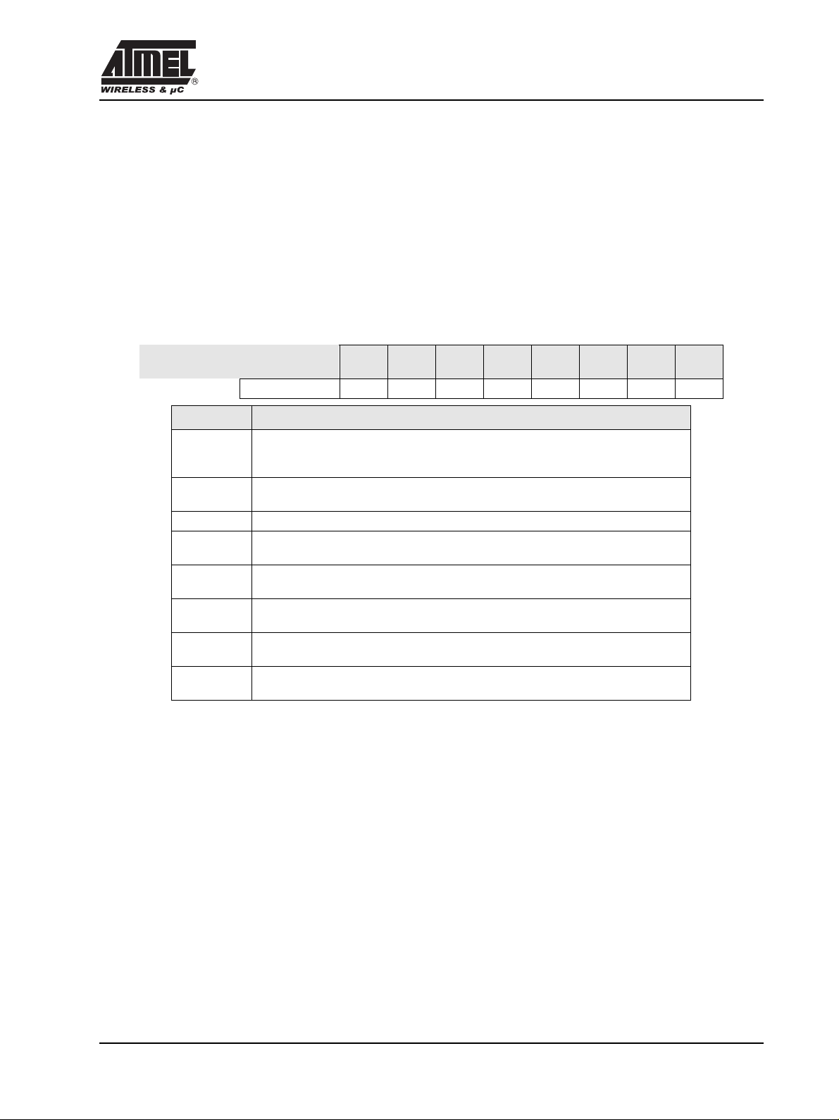
To use one of the PCA modules in the capture mode either one or both of the CCAPM bits CAPN and CAPP for
that module must be set. The external CEX input for the module (on port 1) is sampled for a transition. When a
valid transition occurs the PCA hardware loads the value of the PCA counter registers (CH and CL) into the
module's capture registers (CCAPnL and CCAPnH). If the CCFn bit for the module in the CCON SFR and the
ECCFn bit in the CCAPMn SFR are set then an interrupt will be generated (Refer to Figure 9).
27 Rev. F - 15 February, 2001
Page 28

T89C51RD2
Cex.n
CF CR
ECOMn
CCF4
CAPNn MATn TOGn PWMn ECCFnCAPPn
CCF2 CCF1 CCF0
CCF3
Capture
Figure 9. PCA Capture Mode
CCON
0xD8
PCA IT
PCA Counter/Timer
CH CL
CCAPnH CCAPnL
CCAPMn, n= 0 to 4
0xDA to 0xDE
6.5.2. 16-bit Software Timer / Compare Mode
The PCA modules can be used as software timers by setting both the ECOM and MAT bits in the modules
CCAPMn register. The PCA timer will be compared to the module's capture registers and when a match occurs
an interrupt will occur if the CCFn (CCON SFR) and the ECCFn (CCAPMn SFR) bits for the module are both
set (See Figure 10).
Rev. F - 15 February, 2001 28
Page 29

T89C51RD2
CF CCF2 CCF1 CCF0
CR
CCF4
CCF3
CCON
0xD8
Write to
CCAPnH
Write to
CCAPnL
10
Reset
CCAPnH CCAPnL
Enable
16 bit comparator
CH CL
PCA counter/timer
ECOMn
CIDL CPS1 CPS0 ECF
WDTE
Match
CAPNn MATn TOGn PWMn ECCFnCAPPn
* Only for Module 4
Figure 10. PCA Compare Mode and PCA Watchdog Timer
PCA IT
RESET *
CCAPMn, n = 0 to 4
0xDA to 0xDE
CMOD
0xD9
Before enabling ECOM bit, CCAPnL and CCAPnH should be set with a non zero value, otherwise an unwanted
match could happen. Writing to CCAPnH will set the ECOM bit.
Once ECOM set, writing CCAPnL will clear ECOM so that an unwanted match doesn’t occur while modifying
the compare value. Writing to CCAPnH will set ECOM. For this reason, user software should write CCAPnL first,
and then CCAPnH. Of course, the ECOM bit can still be controlled by accessing to CCAPMn register.
6.5.3. High Speed Output Mode
In this mode the CEX output (on port 1) associated with the PCA module will toggle each time a match occurs
between the PCA counter and the module's capture registers. To activate this mode the TOG, MAT, and ECOM
bits in the module's CCAPMn SFR must be set (See Figure 11).
A prior write must be done to CCAPnL and CCAPnH before writing the ECOMn bit.
29 Rev. F - 15 February, 2001
Page 30

T89C51RD2
CCON
0xD8
PCA IT
CEXn
CCAPMn, n = 0 to 4
0xDA to 0xDE
Write to
CCAPnH
Write to
CCAPnL
1
CF CR
Reset
CCAPnH CCAPnL
0
Enable
16 bit comparator
CH CL
PCA counter/timer
ECOMn
CCF4 CCF3 CCF2 CCF1 CCF0
Match
CAPNn MATn TOGn PWMn ECCFnCAPPn
Figure 11. PCA High Speed Output Mode
Before enabling ECOM bit, CCAPnL and CCAPnH should be set with a non zero value, otherwise an unwanted
match could happen.
Once ECOM set, writing CCAPnL will clear ECOM so that an unwanted match doesn’t occur while modifying
the compare value. Writing to CCAPnH will set ECOM. For this reason, user software should write CCAPnL first,
and then CCAPnH. Of course, the ECOM bit can still be controlled by accessing to CCAPMn register.
6.5.4. Pulse Width Modulator Mode
All of the PCA modules can be used as PWM outputs. Figure 12 shows the PWM function. The frequency of the
output depends on the source for the PCA timer. All of the modules will have the same frequency of output
because they all share the PCA timer. The duty cycle of each module is independently variable using the module's
capture register CCAPLn. When the value of the PCA CL SFR is less than the value in the module's CCAPLn
Rev. F - 15 February, 2001 30
Page 31

T89C51RD2
SFR the output will be low, when it is equal to or greater than the output will be high. When CL overflows from
FF to 00, CCAPLn is reloaded with the value in CCAPHn. This allows updating the PWM without glitches. The
PWM and ECOM bits in the module's CCAPMn register must be set to enable the PWM mode.
Enable
ECOMn
6.5.5. PCA Watchdog Timer
CAPNn MATn TOGn PWMn ECCFnCAPPn
Overflow
CCAPnH
CCAPnL
8 bit comparator
CL
PCA counter/timer
Figure 12. PCA PWM Mode
“0”
<
≥
“1”
CCAPMn, n= 0 to 4
0xDA to 0xDE
CEXn
An on-board watchdog timer is available with the PCA to improve the reliability of the system without increasing
chip count. Watchdog timers are useful for systems that are susceptible to noise, power glitches, or electrostatic
discharge. Module 4 is the only PCA module that can be programmed as a watchdog. However, this module can
still be used for other modes if the watchdog is not needed. Figure 10 shows a diagram of how the watchdog
works. The user pre-loads a 16-bit value in the compare registers. Just like the other compare modes, this 16-bit
value is compared to the PCA timer value. If a match is allowed to occur, an internal reset will be generated. This
will not cause the RST pin to be driven high.
In order to hold off the reset, the user has three options:
• 1. periodically change the compare value so it will never match the PCA timer,
• 2. periodically change the PCA timer value so it will never match the compare values, or
• 3. disable the watchdog by clearing the WDTE bit before a match occurs and then re-enable it.
The first two options are more reliable because the watchdog timer is never disabled as in option #3. If the program
counter ever goes astray, a match will eventually occur and cause an internal reset. The second option is also not
recommended if other PCA modules are being used. Remember, the PCA timer is the time base for all modules;
changing the time base for other modules would not be a good idea. Thus, in most applications the first solution
is the best option.
This watchdog timer won’t generate a reset out on the reset pin.
31 Rev. F - 15 February, 2001
Page 32

T89C51RD2
6.6. Serial I/O Port
The serial I/O port in the T89C51RD2 is compatible with the serial I/O port in the 80C52.
It provides both synchronous and asynchronous communication modes. It operates as an Universal Asynchronous
Receiver and Transmitter (UART) in three full-duplex modes (Modes 1, 2 and 3). Asynchronous transmission and
reception can occur simultaneously and at different baud rates
Serial I/O port includes the following enhancements:
• Framing error detection
• Automatic address recognition
6.6.1. Framing Error Detection
Framing bit error detection is provided for the three asynchronous modes (modes 1, 2 and 3). To enable the framing
bit error detection feature, set SMOD0 bit in PCON register (See Figure 13).
RITIRB8TB8RENSM2SM1SM0/FE
SCON (98h)
Set FE bit if stop bit is 0 (framing error) (SMOD0 = 1)
SM0 to UART mode control (SMOD0 = 0)
PCON (87h)
IDLPDGF0GF1POF-SMOD0SMOD1
To UART framing error control
Figure 13. Framing Error Block Diagram
When this feature is enabled, the receiver checks each incoming data frame for a valid stop bit. An invalid stop
bit may result from noise on the serial lines or from simultaneous transmission by two CPUs. If a valid stop bit
is not found, the Framing Error bit (FE) in SCON register (See Table 15.) bit is set.
Software may examine FE bit after each reception to check for data errors. Once set, only software or a reset can
clear FE bit. Subsequently received frames with valid stop bits cannot clear FE bit. When FE feature is enabled,
RI rises on stop bit instead of the last data bit (See Figure 14. and Figure 15.).
RXD
SMOD0=X
FE
SMOD0=1
Start
bit
RI
Data byte
D7D6D5D4D3D2D1D0
Stop
bit
Figure 14. UART Timings in Mode 1
Rev. F - 15 February, 2001 32
Page 33

T89C51RD2
RXD
RI
SMOD0=0
RI
SMOD0=1
FE
SMOD0=1
Start
bit
Data byte Ninth
D8D7D6D5D4D3D2D1D0
bit
Stop
bit
Figure 15. UART Timings in Modes 2 and 3
6.6.2. Automatic Address Recognition
The automatic address recognition feature is enabled when the multiprocessor communication feature is enabled
(SM2 bit in SCON register is set).
Implemented in hardware, automatic address recognition enhances the multiprocessor communication feature by
allowing the serial port to examine the address of each incoming command frame. Only when the serial port
recognizes its own address, the receiver sets RI bit in SCON register to generate an interrupt. This ensures that
the CPU is not interrupted by command frames addressed to other devices.
If desired, you may enable the automatic address recognition feature in mode 1. In this configuration, the stop bit
takes the place of the ninth data bit. Bit RI is set only when the received command frame address matches the
device’s address and is terminated by a valid stop bit.
To support automatic address recognition, a device is identified by a given address and a broadcast address.
NOTE: The multiprocessor communication and automatic address recognition features cannot be enabled in mode 0 (i.e. setting SM2 bit in SCON
register in mode 0 has no effect).
6.6.3. Given Address
Each device has an individual address that is specified in SADDR register; the SADEN register is a mask byte
that contains don’t-care bits (defined by zeros) to form the device’s given address. The don’t-care bits provide the
flexibility to address one or more slaves at a time. The following example illustrates how a given address is formed.
To address a device by its individual address, the SADEN mask byte must be 1111 1111b.
For example:
SADDR 0101 0110b
SADEN 1111 1100b
Given 0101 01XXb
The following is an example of how to use given addresses to address different slaves:
Slave A: SADDR 1111 0001b
Slave B: SADDR 1111 0011b
Slave C: SADDR 1111 0010b
SADEN 1111 1010b
Given 1111 0X0Xb
SADEN 1111 1001b
Given 1111 0XX1b
SADEN 1111 1101b
Given 1111 00X1b
33 Rev. F - 15 February, 2001
Page 34

T89C51RD2
The SADEN byte is selected so that each slave may be addressed separately.
For slave A, bit 0 (the LSB) is a don’t-care bit; for slaves B and C, bit 0 is a 1. To communicate with slave A
only, the master must send an address where bit 0 is clear (e.g. 1111 0000b).
For slave A, bit 1 is a 1; for slaves B and C, bit 1 is a don’t care bit. To communicate with slaves B and C, but
not slave A, the master must send an address with bits 0 and 1 both set (e.g. 1111 0011b).
To communicate with slaves A, B and C, the master must send an address with bit 0 set, bit 1 clear, and bit 2
clear (e.g. 1111 0001b).
6.6.4. Broadcast Address
A broadcast address is formed from the logical OR of the SADDR and SADEN registers with zeros defined as
don’t-care bits, e.g.:
SADDR 0101 0110b
SADEN 1111 1100b
Broadcast =SADDR OR SADEN 1111 111Xb
The use of don’t-care bits provides flexibility in defining the broadcast address, however in most applications, a
broadcast address is FFh. The following is an example of using broadcast addresses:
Slave A: SADDR 1111 0001b
SADEN 1111 1010b
Broadcast 1111 1X11b,
Slave B: SADDR 1111 0011b
Slave C: SADDR= 1111 0010b
For slaves A and B, bit 2 is a don’t care bit; for slave C, bit 2 is set. To communicate with all of the slaves, the
master must send an address FFh. To communicate with slaves A and B, but not slave C, the master can send
and address FBh.
SADEN 1111 1001b
Broadcast 1111 1X11B,
SADEN 1111 1101b
Broadcast 1111 1111b
6.6.5. Reset Addresses
On reset, the SADDR and SADEN registers are initialized to 00h, i.e. the given and broadcast addresses are XXXX
XXXXb (all don’t-care bits). This ensures that the serial port will reply to any address, and so, that it is backwards
compatible with the 80C51 microcontrollers that do not support automatic address recognition.
SADEN - Slave Address Mask Register (B9h)
7 6 5 4 3 2 1 0
Reset Value = 0000 0000b
Not bit addressable
SADDR - Slave Address Register (A9h)
7 6 5 4 3 2 1 0
Reset Value = 0000 0000b
Not bit addressable
Table 15. SCON Register
Rev. F - 15 February, 2001 34
Page 35

T89C51RD2
SCON - Serial Control Register (98h)
7 6 5 4 3 2 1 0
FE/SM0 SM1 SM2 REN TB8 RB8 TI RI
Bit
Number
7 FE
6 SM1
5 SM2
4 REN
3 TB8
Bit
Mnemonic
SM0
Description
Framing Error bit (SMOD0=1)
Clear to reset the error state, not cleared by a valid stop bit.
Set by hardware when an invalid stop bit is detected.
SMOD0 must be set to enable access to the FE bit
Serial port Mode bit 0
Refer to SM1 for serial port mode selection.
SMOD0 must be cleared to enable access to the SM0 bit
Serial port Mode bit 1
SM0 SM1 Mode Description Baud Rate
0 0 0 Shift Register F
0 1 1 8-bit UART Variable
1 0 2 9-bit UART F
1 1 3 9-bit UART Variable
Serial port Mode 2 bit / Multiprocessor Communication Enable bit
Clear to disable multiprocessor communication feature.
Set to enable multiprocessor communication feature inmode 2 and 3, and eventuallymode 1. This bitshould
be cleared in mode 0.
Reception Enable bit
Clear to disable serial reception.
Set to enable serial reception.
Transmitter Bit 8 / Ninth bit to transmit in modes 2 and 3.
Clear to transmit a logic 0 in the 9th bit.
Set to transmit a logic 1 in the 9th bit.
/12 (/6 in X2 mode)
XTAL
/64 or F
XTAL
/32 (/32 or 16 in X2 mode)
XTAL
2 RB8
1 TI
0 RI
Reset Value = 0000 0000b
Bit addressable
Receiver Bit 8 / Ninth bit received in modes 2 and 3
Cleared by hardware if 9th bit received is a logic 0.
Set by hardware if 9th bit received is a logic 1.
In mode 1, if SM2 = 0, RB8 is the received stop bit. In mode 0 RB8 is not used.
Transmit Interrupt flag
Clear to acknowledge interrupt.
Set by hardware at the end of the 8th bit time in mode 0 or at the beginning of the stop bit in the other
modes.
Receive Interrupt flag
Clear to acknowledge interrupt.
Set by hardware at the end of the 8th bit time in mode 0, see Figure 14. and Figure 15. in the other modes.
35 Rev. F - 15 February, 2001
Page 36

T89C51RD2
Table 16. PCON Register
PCON - Power Control Register (87h)
7 6 5 4 3 2 1 0
SMOD1 SMOD0 - POF GF1 GF0 PD IDL
Bit
Number
7 SMOD1
6 SMOD0
5 -
4 POF
3 GF1
2 GF0
1 PD
0 IDL
Bit
Mnemonic
Description
Serial port Mode bit 1
Set to select double baud rate in mode 1, 2 or 3.
Serial port Mode bit 0
Clear to select SM0 bit in SCON register.
Set to to select FE bit in SCON register.
Reserved
The value read from this bit is indeterminate. Do not set this bit.
Power-Off Flag
Clear to recognize next reset type.
Set by hardware when VCC rises from 0 to its nominal voltage. Can also be set by software.
General purpose Flag
Cleared by user for general purpose usage.
Set by user for general purpose usage.
General purpose Flag
Cleared by user for general purpose usage.
Set by user for general purpose usage.
Power-Down mode bit
Cleared by hardware when reset occurs.
Set to enter power-down mode.
Idle mode bit
Clear by hardware when interrupt or reset occurs.
Set to enter idle mode.
Reset Value = 00X1 0000b
Not bit addressable
Power-off flag reset value will be 1 only after a power on (cold reset). A warm reset doesn’t affect the value of this bit.
Rev. F - 15 February, 2001 36
Page 37

T89C51RD2
6.7. Interrupt System
The T89C51RD2 has a total of 7 interrupt vectors: two external interrupts (INT0 and INT1), three timer interrupts
(timers 0, 1 and 2), the serial port interrupt and the PCA global interrupt. These interrupts are shown in Figure 16.
INT0
TF0
INT1
TF1
PCA IT
RI
TI
TF2
EXF2
IE0
IE1
IPH, IP
High priority
interrupt
3
0
3
0
3
0
3
0
3
0
3
0
3
0
Interrupt
polling
sequence, decreasing
from high to low priority
Individual Enable
Global Disable
Low priority
interrupt
Figure 16. Interrupt Control System
Each of the interrupt sources can be individually enabled or disabled by setting or clearing a bit in the Interrupt
Enable register (See Table 18.). This register also contains a global disable bit, which must be cleared to disable
all interrupts at once.
Each interrupt source can also be individually programmed to one out of four priority levels by setting or clearing
a bit in the Interrupt Priority register (See Table 19.) and in the Interrupt Priority High register (See Table 20.).
shows the bit values and priority levels associated with each combination.
The PCA interrupt vector is located at address 0033H. All other vectors addresses are the same as standard C52
devices.
Rev. F - 15 February, 2001 37
Page 38

T89C51RD2
Table 17. Priority Level Bit Values
IPH.x IP.x Interrupt Level Priority
0 0 0 (Lowest)
0 1 1
1 0 2
1 1 3 (Highest)
A low-priority interrupt can be interrupted by a high priority interrupt, but not by another low-priority interrupt.
A high-priority interrupt can’t be interrupted by any other interrupt source.
If two interrupt requests of different priority levels are received simultaneously, the request of higher priority level
is serviced. If interrupt requests of the same priority level are received simultaneously, an internal polling sequence
determines which request is serviced. Thus within each priority level there is a second priority structure determined
by the polling sequence.
Table 18. IE Register
IE - Interrupt Enable Register (A8h)
7 6 5 4 3 2 1 0
EA EC ET2 ES ET1 EX1 ET0 EX0
Bit
Number
7 EA
6 EC
5 ET2
4 ES
3 ET1
2 EX1
1 ET0
Bit
Mnemonic
Description
Enable All interrupt bit
Clear to disable all interrupts.
Set to enable all interrupts.
If EA=1, each interrupt source is individually enabled or disabled by setting or clearing its own interrupt
enable bit.
PCA interrupt enable bit
Clear to disable . Set to enable.
Timer 2 overflow interrupt Enable bit
Clear to disable timer 2 overflow interrupt.
Set to enable timer 2 overflow interrupt.
Serial port Enable bit
Clear to disable serial port interrupt.
Set to enable serial port interrupt.
Timer 1 overflow interrupt Enable bit
Clear to disable timer 1 overflow interrupt.
Set to enable timer 1 overflow interrupt.
External interrupt 1 Enable bit
Clear to disable external interrupt 1.
Set to enable external interrupt 1.
Timer 0 overflow interrupt Enable bit
Clear to disable timer 0 overflow interrupt.
Set to enable timer 0 overflow interrupt.
0 EX0
External interrupt 0 Enable bit
Clear to disable external interrupt 0.
Set to enable external interrupt 0.
Reset Value = 0000 0000b
Bit addressable
38 Rev. F - 15 February, 2001
Page 39

T89C51RD2
Table 19. IP Register
IP - Interrupt Priority Register (B8h)
7 6 5 4 3 2 1 0
- PPC PT2 PS PT1 PX1 PT0 PX0
Bit
Number
7 -
6 PPC
5 PT2
4 PS
3 PT1
2 PX1
1 PT0
0 PX0
Bit
Mnemonic
Reset Value = X000 0000b
Bit addressable
Description
Reserved
The value read from this bit is indeterminate. Do not set this bit.
PCA interrupt priority bit
Refer to PPCH for priority level.
Timer 2 overflow interrupt Priority bit
Refer to PT2H for priority level.
Serial port Priority bit
Refer to PSH for priority level.
Timer 1 overflow interrupt Priority bit
Refer to PT1H for priority level.
External interrupt 1 Priority bit
Refer to PX1H for priority level.
Timer 0 overflow interrupt Priority bit
Refer to PT0H for priority level.
External interrupt 0 Priority bit
Refer to PX0H for priority level.
Rev. F - 15 February, 2001 39
Page 40

T89C51RD2
Table 20. IPH Register
IPH - Interrupt Priority High Register (B7h)
7 6 5 4 3 2 1 0
- PPCH PT2H PSH PT1H PX1H PT0H PX0H
Bit
Number
7 -
6 PPCH
5 PT2H
4 PSH
3 PT1H
Bit
Mnemonic
Description
Reserved
The value read from this bit is indeterminate. Do not set this bit.
PCA interrupt priority bit high.
PPCHPPC Priority Level
0 0 Lowest
01
10
1 1 Highest
Timer 2 overflow interrupt Priority High bit
PT2HPT2 Priority Level
0 0 Lowest
01
10
1 1 Highest
Serial port Priority High bit
PSHPS Priority Level
0 0 Lowest
01
10
1 1 Highest
Timer 1 overflow interrupt Priority High bit
PT1HPT1 Priority Level
0 0 Lowest
01
10
1 1 Highest
External interrupt 1 Priority High bit
PX1HPX1 Priority Level
2 PX1H
1 PT0H
0 PX0H
0 0 Lowest
01
10
1 1 Highest
Timer 0 overflow interrupt Priority High bit
PT0HPT0 Priority Level
0 0 Lowest
01
10
1 1 Highest
External interrupt 0 Priority High bit
PX0HPX0 Priority Level
0 0 Lowest
01
10
1 1 Highest
Reset Value = X000 0000b
Not bit addressable
40 Rev. F - 15 February, 2001
Page 41

T89C51RD2
6.8. Idle mode
An instruction that sets PCON.0 causes that to be the last instruction executed before going into the Idle mode.
In the Idle mode, the internal clock signal is gated off to the CPU, but not to the interrupt, Timer, and Serial Port
functions. The CPU status is preserved in its entirely : the Stack Pointer, Program Counter, Program Status Word,
Accumulator and all other registers maintain their data during Idle. The port pins hold the logical states they had
at the time Idle was activated. ALE and PSEN hold at logic high levels.
There are two ways to terminate the Idle. Activation of any enabled interrupt will cause PCON.0 to be cleared by
hardware, terminating the Idle mode. The interrupt will be serviced, and following RETI the next instruction to
be executed will be the one following the instruction that put the device into idle.
The flag bits GF0 and GF1 can be used to give an indication if an interrupt occured during normal operation or
during an Idle. For example, an instruction that activates Idle can also set one or both flag bits. When Idle is
terminated by an interrupt, the interrupt service routine can examine the flag bits.
The other way of terminating the Idle mode is with a hardware reset. Since the clock oscillator is still running,
the hardware reset needs to be held active for only two machine cycles (24 oscillator periods) to complete the reset.
6.9. Power-Down Mode
To save maximum power, a power-down mode can be invoked by software (refer to Table 13, PCON register).
In power-down mode, the oscillator is stopped and the instruction that invoked power-down mode is the last
instruction executed. The internal RAM and SFRs retain their value until the power-down mode is terminated.
VCCcan be lowered to save further power. Either a hardware reset or an external interrupt can cause an exit from
power-down. To properly terminate power-down, the reset or external interrupt should not be executed before V
is restored to its normal operating level and must be held active long enough for the oscillator to restart and stabilize.
CC
Only external interrupts INT0 and INT1 are useful to exit from power-down. For that, interrupt must be enabled
and configured as level or edge sensitive interrupt input.
Holding the pin low restarts the oscillator but bringing the pin high completes the exit as detailed in Figure 17..
When both interrupts are enabled, the oscillator restarts as soon as one of the two inputs is held low and power
down exit will be completed when the first input will be released. In this case the higher priority interrupt service
routine is executed.
Once the interrupt is serviced, the next instruction to be executed after RETI will be the one following the instruction
that put Lynx/Fox into power-down mode.
INT0
INT1
XTAL1
Power-down phase Oscillator restart phase Active phaseActive phase
Figure 17. Power-Down Exit Waveform
Exit from power-down by reset redefines all the SFRs, exit from power-down by external interrupt does no affect
the SFRs.
Exit from power-down by either reset or external interrupt does not affect the internal RAM content.
NOTE:If idle modeis activated with power-down mode (IDL and PD bits set), the exit sequence is unchanged,when execution is vectored to interrupt,
PD and IDL bits are cleared and idle mode is not entered.
Rev. F - 15 February, 2001 41
Page 42

T89C51RD2
This table shows the state of ports during idle and power-down modes.
Mode
Idle Internal 1 1 Port Data* Port Data Port Data Port Data
Idle External 1 1 Floating Port Data Address Port Data
Power Down Internal 0 0 Port Dat* Port Data Port Data Port Data
Power Down External 0 0 Floating Port Data Port Data Port Data
* Port 0 can force a 0 level. A "one" will leave port floating.
Program
Memory
ALE PSEN PORT0 PORT1 PORT2 PORT3
42 Rev. F - 15 February, 2001
Page 43

T89C51RD2
6.10. Hardware Watchdog Timer
The WDT is intended as a recovery method in situations where the CPU may be subjected to software upset. The
WDT consists of a 14-bit counter and the WatchDog Timer ReSeT (WDTRST) SFR. The WDT is by default
disabled from exiting reset. To enable the WDT, user must write 01EH and 0E1H in sequence to the WDTRST,
SFR location 0A6H. When WDT is enabled, it will increment every machine cycle while the oscillator is running
and there is no way to disable the WDT except through reset (either hardware reset or WDT overflow reset). When
WDT overflows, it will drive an output RESET HIGH pulse at the RST-pin.
6.10.1. Using the WDT
To enable the WDT, user must write 01EH and 0E1H in sequence to the WDTRST, SFR location 0A6H. When
WDT is enabled, the user needs to service it by writing to 01EH and 0E1H to WDTRST to avoid WDT overflow.
The 14-bit counter overflows when it reaches 16383 (3FFFH) and this will reset the device. When WDT is enabled,
it will increment every machine cycle while the oscillator is running. This means the user must reset the WDT at
least every 16383 machine cycle. To reset the WDT the user must write 01EH and 0E1H to WDTRST. WDTRST
is a write only register. The WDT counter cannot be read or written. When WDT overflows, it will generate an
output RESET pulse at the RST-pin. The RESET pulse duration is 96 x T
the best use of the WDT, it should be serviced in those sections of code that will periodically be executed within
the time required to prevent a WDT reset.
To have a more powerful WDT, a 27counter has been added to extend the Time-out capability, ranking from
16ms to 2s @ F
= 12MHz. To manage this feature, refer to WDTPRG register description, Table 22. (SFR0A7h).
OSC
OSC
, where T
OSC
= 1/F
OSC
. To make
Table 21. WDTRST Register
WDTRST Address (0A6h)
7 6 5 4 3 2 1
Reset value X X X X X X X
Write only, this SFR is used to reset/enable the WDT by writing 01EH then 0E1H in sequence.
Rev. F - 15 February, 2001 43
Page 44

T89C51RD2
Table 22. WDTPRG Register
WDTPRG Address (0A7h)
7 6 5 4 3 2 1 0
T4 T3 T2 T1 T0 S2 S1 S0
Bit
Number
7 T4
6 T3
5 T2
4 T1
3 T0
2 S2 WDT Time-out select bit 2
1 S1 WDT Time-out select bit 1
0 S0 WDT Time-out select bit 0
Bit
Mnemonic
Reserved
The value read from this bit is undeterminated. Do not try to set this bit..
S2 S1S0 Selected Time-out
000 (214 - 1) machine cycles, 16.3 ms @ 12 MHz
001 (2
010 (216 - 1) machine cycles, 65.5 ms @ 12 MHz
011 (2
100 (218 - 1) machine cycles, 262 ms @ 12 MHz
101 (2
110 (220 - 1) machine cycles, 1.05 s @ 12 MHz
111 (2
Reset value XXXX X000
Description
15
- 1) machine cycles, 32.7 ms @ 12 MHz
17
- 1) machine cycles, 131 ms @ 12 MHz
19
- 1) machine cycles, 542 ms @ 12 MHz
21
- 1) machine cycles, 2.09 s @ 12 MHz
6.10.2. WDT during Power Down and Idle
In Power Down mode the oscillator stops, which means the WDT also stops. While in Power Down mode the
user does not need to service the WDT. There are 2 methods of exiting Power Down mode: by a hardware reset
or via a level activated external interrupt which is enabled prior to entering Power Down mode. When Power
Down is exited with hardware reset, servicing the WDT should occur as it normally should whenever the T89C51RD2
is reset. Exiting Power Down with an interrupt is significantly different. The interrupt is held low long enough for
the oscillator to stabilize. When the interrupt is brought high, the interrupt is serviced. To prevent the WDT from
resetting the device while the interrupt pin is held low, the WDT is not started until the interrupt is pulled high.
It is suggested that the WDT be reset during the interrupt service routine.
To ensure that the WDT does not overflow within a few states of exiting of powerdown, it is best to reset the
WDT just before entering powerdown.
In the Idle mode, the oscillator continues to run. To prevent the WDT from resetting the T89C51RD2 while in
Idle mode, the user should always set up a timer that will periodically exit Idle, service the WDT, and re-enter
Idle mode.
If the WDT is activated, the power consumption in stand-by mode will be above the specified value.
44 Rev. F - 15 February, 2001
Page 45

T89C51RD2
6.11. ONCE
The ONCE mode facilitates testing and debugging of systems using T89C51RD2 without removing the circuit
from the board. The ONCE mode is invoked by driving certain pins of the T89C51RD2; the following sequence
must be exercised:
(TM)
Mode (ON Chip Emulation)
• Pull ALE low while the device is in reset (RST high) and PSEN is high.
• Hold ALE low as RST is deactivated.
While the T89C51RD2 is in ONCE mode, an emulator or test CPU can be used to drive the circuit. Table 23.
shows the status of the port pins during ONCE mode.
Normal operation is restored when normal reset is applied.
Table 23. External Pin Status during ONCE Mode
ALE PSEN Port 0 Port 1 Port 2 Port 3 XTAL1/2
Weak pull-up Weak pull-up Float Weak pull-up Weak pull-up Weak pull-up Active
(a) "Once" is a registered trademark of Intel Corporation.
Rev. F - 15 February, 2001 45
Page 46

T89C51RD2
6.12. Reduced EMI Mode
The ALE signal is used to demultiplex address and data buses on port 0 when used with external program or data
memory. Nevertheless, during internal code execution, ALE signal is still generated. In order to reduce EMI, ALE
signal can be disabled by setting AO bit.
The AO bit is located in AUXR register at bit location 0. As soon as AO is set, ALE is no longer output but
remains active during MOVX and MOVC instructions and external fetches. During ALE disabling, ALE pin is
weakly pulled high.
Table 24. AUXR Register
AUXR - Auxiliary Register (8Eh)
7 6 5 4 3 2 1 0
- - M0 - XRS1 XRS0 EXTRAM AO
Bit
Number
7 -
6 -
5 M0
4 -
3 XRS1
2 XRS0
1 EXTRAM
0 AO
Bit
Mnemonic
Reserved
Reserved
M0 bit: Pulse length in clock period
Reserved
XRS1 bit
XRS0 bit
EXTRAM bit
ALE Output bit
Reset Value = XX0X 1000b
Not bit addressable
Description
The value read from this bit is indeterminate. Do not set this bit.
The value read from this bit is indeterminate. Do not set this bit.
StretchMOVX control: the RD/and the WR/ pulse lengthis increased according tothe value of M0. see table 6
The value read from this bit is indeterminate. Do not set this bit.
XRAM size: Accessible size of the XRAM. See Table 6.
XRAM size: Accessible size of the XRAM. Table 6.
See Table 6.
Clear to restore ALE operation during internal fetches.
Set to disable ALE operation during internal fetches.
Rev. F - 15 February, 2001 46
Page 47

T89C51RD2
7. EEPROM data memory
7.1. General description
The EEPROM memory block contains 2048 bytes and is organized in 32 pages (or rows) of 64 bytes. The necessary
high programming voltage is generated on-chip using the standard Vcc pin of the microcontroller.
The EEPROM memory block is located at the addresses 0000h to 07FFh of the XRAM memory space and is
selected by setting control bits in the EECON register.
A read in the EEPROM memory is done with a MOVX instruction.
A physical write in the EEPROM memory is done in two steps : write data in the column latches and transfer of
all data latches in a EEPROM memory row (programming).
The number of data written in the page may vary from 1 to 64 (the page size). When programming, only the data
written in the column latch are programmed. This provides the capability to program the whole memory by bytes,
by page or by a number of bytes in a page.
7.2. Write Data in the column latches
Data is written by byte to the column latches as if it was in an external RAM memory. Out of the 16 address bits
of the data pointer, the 10 MSB are used for page selection and 6 are used for byte selection. Between two
EEPROM programming, all addresses in the column latches must remain in the same page, thus the 10MSB must
be unchanged.
The following procedure is used to write in the colums latches :
• Map the program space (Set bit EEE of EECON register)
• Load DPTR with the address to write
• Load A register with the data to be written
• Execute a MOVX @DPTR, A
• If needed loop the three last instructions until the end of a 64bytes page
7.3. Programming
The EEPROM programming consists on the following actions :
• write one or more bytes in a page in the column latches. Normally, all bytes must belong to the same page;
if this is not the case, the first page address is latched and the others are discarded.
• Set EETIM with the value corresponding to the XTAL frequency.
• Launch the programming by writing the control sequence (52h or 50h followed by A2h or A0h) to the EECON
register (see Table 25).
• EEBUSY flag in EECON is then set by hardware to indicate that programming is in progress and that EEPROM
segment is not available for read.
• The end of programming is signaled by a hardware clear of the EEBUSY flag.
Rev. F - 15 February, 2001 47
Page 48

T89C51RD2
Example : ..... ; DPTR = EEPROM data pointer, A = Data to write
Wait : MOV A,EECON
ANL A,#01h
JNZ Wait
MOV EETIM,#3Ch ; 12MHz*5 = 3Ch
MOV EECON,#02h ; EEE=1 EEPROM mapped
MOVX @DPTR,A ; Write data to EEPROM
MOV EECON,#50h or 52h ; Write Sequence
MOV EECON,#A0h or A2h
....
7.4. Read Data
The following procedure is used to read the data store in the EEPROM memory:
• Map the program space (Set bit EEE of EECON register)
• Load DPTR with the address to read
• Execute a MOVX A, @DPTR
Example : ... ; DPTR = EEPROM data pointer
MOV EECON,#02h ; EEE=1 EEPROM mapped
MOVX A,@DPTR ; Read data from EEPROM
... ; A = Data
7.5. Registers
Table 25. EECON Register
EECON (S:0D2h)
EEPROM Control Register
76543210
EEPL3 EEPL2 EEPL1 EEPL0 - - EEE EEBUSY
Bit Number Bit Mnemonic Description
7-4 EEPL3-0
3 - Not implemented, reserved for future use.
2 - Not implemented, reserved for future use.
1 EEE
0 EEBUSY
a. User software should not write 1s to reserved bits. These bits may be used in future 8051 family products to invoke new features. In
that case, the reset or inactive value of the new bit will be 0, and its active value will be 1. The value read from a reserved bit is
indeterminate.
b. User software should not write 1s to reserved bits. These bits may be used in future 8051 family products to invoke new features. In
that case, the reset or inactive value of the new bit will be 0, and its active value will be 1. The value read from a reserved bit is
indeterminate.
Programming Launch command bits
Write 5Xh followed by AXh to EECON to launch the programming.
a
b
Enable EEPROM Space bit
Set to map the EEPROM space during MOVX instructions (Write in the column latches)
Clear to map the data space during MOVX.
Programming Busy flag
Set by hardware when programming is in progress.
Cleared by hardware when programming is done.
Can not be set or cleared by software.
Reset Value= XXXX XX00b
48 Rev. F - 15 February, 2001
Page 49

T89C51RD2
Table 26. EETIM Register
EETIM (S:0D3h)
EEPROM timing Control Register
76543210
EETIM
Bit Number Bit Mnemonic Description
Write Timer Register
7-0 EETIM
Reset Value= 0000 0000b
The write timer register value is required to adapt the write time to the oscillator frequency
Value = 5 * Fxtal (MHz) in normal mode, 10 * Fxtal in X2 mode.
Example : Fxtal = 33 MHZ, EETIM = 0A5h
Rev. F - 15 February, 2001 49
Page 50

T89C51RD2
8. FLASH EEprom Memory
8.1. General description
The FLASH memory increases EPROM and ROM functionality with in-circuit electrical erasure and programming.
It contains 64K bytes of program memory organized in 512 pages of 128 bytes. This memory is both parallel and
serial In-System Programmable (ISP). ISP allows devices to alter their own program memory in the actual end
product under software control. A default serial loader (bootloader) program allows ISP of the FLASH.
The programming does not require 12v external programming voltage. The necessary high programming voltage
is generated on-chip using the standard VCCpins of the microcontroller.
8.2. Features
FLASH E2PROM internal program memory.
•
• The last 1K bytes of the FLASH is used to store the low-level in-system programming routines and a default
serial loader. If the application does not need to use the ISP and does not expect to modify the FLASH content,
the Boot FLASH sector can be erased to provide access to the full 64K byte FLASH memory.
• Boot vector allows user provided FLASH loader code to reside anywhere in the FLASH memory space. This
configuration provides flexibility to the user.
• Default loader in Boot FLASH allows programming via the serial port without the need of a user provided loader.
• Up to 64K byte external program memory if the internal program memory is disabled (EA = 0).
• Programming and erase voltage with standard 5V or 3V V
• Read/Programming/Erase:
• Byte-wise read (without wait state).
• Byte or page erase and programming (10 ms).
• Typical programming time (63K bytes) in 20 s.
• Parallel programming with 87C51 compatible hardware interface to programmer.
• Programmable security for the code in the FLASH.
• 100k write cycles
• 10 years data retention
CC
supply.
8.3. FLASH Programming and Erasure
The 64K bytes FLASH is programmed by bytes or by pages of 128 bytes. It is not necessary to erase a byte or
a page before programming. The programming of a byte or a page includes a self erase before programming.
There are three methods to program the FLASH memory:
• First, the on-chip ISP bootloader may be invoked which will use low level routines to program the pages. The
interface used for serial downloading of FLASH is the UART.
• Second, the FLASH may be programmed or erased in the end-user application by calling low-level routines
through a common entry point in the Boot loader.
• Third, the FLASH may be programmed using the parallel method by using a conventional EPROM programmer.
The parallel programming method used by these devices is similar to that used by EPROM 87C51 but it is not
identical and the commercially available programmers need to have support for the T89C51RD2.
Rev. F - 15 February, 2001 50
Page 51

T89C51RD2
The bootloader and the In Application Programming (IAP) routines are located in the last kilobyte of the FLASH,
leaving 63k bytes available for the application with ISP.
8.4. FLASH registers and memory map
The T89C51RD2 FLASH memory uses several registers for his management:
• Flash control register is used to select the Flash memory spaces and launch the Flash programming sequence.
• Hardware registers can only be accessed through the parallel programming modes which are handled by the
parallel programmer.
• Software registers are in a special page of the FLASH memory which can be accessed through the API or with
the parallel programming modes. This page, called "Extra FLASH Memory", is not in the internal FLASH
program memory addressing space.
8.4.1. FLASH register
FCON (S:D1h)
FLASH control register
76543210
FPL3 FPL2 FPL1 FPL0 FPS FMOD1 FMOD0 FBUSY
Bit Number BitMnemonic Description
7-4 FPL3:0
3 FPS
2-1 FMOD1:0
0 FBUSY
Programming Launch command bits
Write 5h followed by Ah to launch the programming.
FLASH Map Program Space
Clear to map the data space during MOVX
Set to map the FLASH space during MOVX (write) or MOVC (read) instructions (Write in the
column latches)
FLASH Mode
Select the addressed space
00: User (0000h-FFFFh)
01: XAF
10: Hardware byte
11: reserved
FLASH Busy
Set by hardware when programming is in progress.
Clear by hardware when programming is done.
Can not be cleared by software
Reset Value = xxxx 0000b
Figure 18. FCON register
The Flash programming application note and API source code are available on request.
8.4.2. Hardware register
The only hardware register of the T89C51RD2 is called Hardware Security Byte (HSB). After full FLASH erasure,
the content of this byte is FFh; each bit is active at low level.
51 Rev. F - 15 February, 2001
Page 52

T89C51RD2
Table 27. Hardware Security Byte (HSB)
7 6 5 4 3 2 1 0
SB BLJB BLLB - - LB2 LB1 LB0
Bit
Number
7 SB
6 BLJB
5 BLLB
4 -
3 -
2-0 LB2-0
Bit
Mnemonic
Description
Safe Bit
This bit must be cleared to secure the content of the HSB. Only security level can be increased.
Boot loader Jump Bit
Set to force hardware boot address at 0000h. (unless previously force by hardware conditions as
described in the chapter 9.6).
Clear to force hardware boot address at FC03h (default).
Boot loader Lock Bit
Set to allow programming and writing of the boot loader segment.
Clear to forbid software programming and writing of the boot loader segment (default). This protection protect
only ISP or IAP access; protection through parallel access is done globally by the lock bits LB2-0.
Reserved
Do not clear this bit.
Reserved
Do not clear this bit.
User Memory Lock Bits
See Table 29
8.4.2.1. Boot Loader Lock Bit (BLLB)
One bit of the HSB is used to secure by hardware the internal boot loader sector against software reprogramming.
When the BLLB is cleared, any attempt to write in the boot loader segment (Address FC00h to FFFFh) will have
no effect. This protection applies for software writing only.
Boot Loader Jump Bit (BLJB)
One bit of the HSB, the BLJB bit, is used to force the boot address:
• When this bit is set the boot address is 0000h.
• When this bit is reset the boot address is FC03h. By default, this bit is cleared and the ISP is enabled.
8.4.2.2. FLASH memory lock bits
The three lock bits provide different levels of protection for the on-chip code and data, when programmed according
to Table 29.
Rev. F - 15 February, 2001 52
Page 53

T89C51RD2
Table 28. Program Lock bits
Program Lock Bits
Security
level
1 U U U
2 P U U
3 X P U Same as 2, also verify through parallel programming interface is disabled.
4 X X P Same as 3, also external execution is disabled.
U: unprogrammed or "one" level.
P: programmed or "zero" level.
X:do not care
WARNING: Security level 2 and 3 should only be programmed after FLASH and code verification.
LB0 LB1 LB2
Noprogram lock features enabled. MOVCinstruction executedfromexternal program
memory returns non encrypted data.
MOVCinstruction executed from externalprogram memory are disabled from fetching
code bytes from internal memory,
parallel programming of the FLASH is disabled.ISP and software programming with
API are still allowed.
Protection description
EA is sampled and latched on reset, and further
These security bits protect the code access through the parallel programming interface. They are set by default to
level 4. The code access through the ISP is still possible and is controlled by the "software security bits" which
are stored in the extra FLASH memory accessed by the ISP firmware.
To load a new application with the parallel programmer, a chip erase must first be done. This will set the HSB
in its inactive state and will erase the FLASH memory, including the boot loader and the "Extra FLASH Memory"
(XAF). If needed, the 1K boot loader and the XAF content must be programmed in the FLASH; the code is
provided by ATMEL Wireless and Microcontrollers (see section 8.7. ); the part reference can always be read using
FLASH parallel programming modes.
8.4.2.3. Default values
The default value of the HSB provides parts ready to be programmed with ISP:
• SB: Cleared to secure the content of the HSB.
• BLJB: Cleared to force ISP operation.
• BLLB: Clear to protect the default boot loader.
• LB2-0: Security level four to protect the code from a parallel access with maximum security.
8.4.3. Software registers
Several registers are used, in factory and by parallel programmers, to make copies of hardware registers contents.
These values are used by ATMEL Wireless and Microcontrollers ISP (see section 8.7. ).
These registers are in the "Extra FLASH Memory" part of the FLASH memory. This block is also called "XAF"
or eXtra Array FLASH. They are accessed in the following ways:
• Commands issued by the parallel memory programmer.
• Commands issued by the ISP software.
• Calls of API issued by the application software.
53 Rev. F - 15 February, 2001
Page 54

T89C51RD2
They are several software registers described in Table 29
Table 29. Default values
Mnemonic Default value
BSB
SBV
HSB
SSB
Boot Status Byte
Software Boot Vector
Copy of the Hardware security byte
Software Security Byte
Copy of the Manufacturer Code
Copy of the Device ID #1: Family Code
Copy of the Device ID #2: memories
size and type
Copy of the Device ID # 3: name and revi-
sion
After programming the part by ISP, the BSB must be reset (00h) in order to allow the application to boot at 0000h.
The content of the Software Security Byte (SSB) is described in Table 30 and Table 31
FFh
FCh
18h or 1Bh
FFh
58h
D7h C51 X2, Electrically Erasable
FCh
FFh
ATMEL Wireless and
Microcontrollers
T89C51RD2 memories size
T89C51RD2, revision 0
To assure code protection from a parallel access, the HSB must also be at the required level.
Table 30. Software Security Byte (SSB)
7 6 5 4 3 2 1 0
- - - LB1 - - - LB0
Bit
Number
7 -
6 -
5 -
4 LB1
1-3 -
0 LB0
Bit
Mnemonic
Description
Reserved
Do not clear this bit.
Reserved
Do not clear this bit.
Reserved
Do not clear this bit.
User Memory Lock Bit
See Table 31
Reserved
Do not clear this bit.
User Memory Lock Bit
See Table 31
The three lock bits provide different levels of protection for the on-chip code and data, when programmed according
to Table 31.
Rev. F - 15 February, 2001 54
Page 55

T89C51RD2
Table 31. Program Lock bits of the SSB
Program Lock Bits
Security
level
1 U U No program lock features enabled.
2 P U
3 X P
U: unprogrammed or "one" level.
P: programmed or "zero" level.
X:do not care
WARNING: Security level 2 and 3 should only be programmed after FLASH and code verification.
LB0 LB1
following commands are disabled:
- program byte
- program status byte and boot vector
- erase status byte and boot vector
Same as 2 and following commands also disabled:
- read byte
- read status byte and boot vector
- blank check
- program SSB level2
Protection description
8.5. FLASH memory status
T89C51RD2 parts are delivered in standard with the ISP boot in the FLASH memory. After ISP or parallel
programming, the possible contents of the FLASH memory are summarized on the figure below:
Figure 19. FLASH memory possible contents
FC00h
Boot
Virgin
Boot Boot
Boot
Virgin
ApplicationApplication
Virgin
Boot
Virgin
or appli or appli or appli
Dedicated
ISP
Dedicated
ISP
0000h
Default
After ISP
After ISP
After parallel
programming
After parallel
programming
After parallel
programming
8.6. Boot process
Boot loader FLASH
When the user application programs its own FLASH memory, all of the low level details are handled by a code
that is permanently contained in a 1k byte “Boot FLASH” and is located in the last kilobyte of the FLASH memory
from FC00h to FFFFh (See Figure 20). A user program simply calls the common entry point in the Boot FLASH
with appropriate parameters to accomplish the desired operation. Boot FLASH operations include functions like:
55 Rev. F - 15 February, 2001
Page 56

T89C51RD2
erase block, program byte or page, verify byte or page, program security lock bit, etc. The Boot FLASH can be
locked to prevent erasing. If erased, the Boot FLASH can be restored by parallel programming. Indeed, ATMEL
Wireless and Microcontrollers provides the binary code of the default FLASH boot loader (see section 8.7. ).
FFF0
FC03
FC00
Figure 20. Boot loader memory map
Entry point for API
Status byte check
ISP start
Reset Code Execution
At the falling edge of reset (unless the hardware conditions on PSEN, EA and ALE are set as described below),
the T89C51RD2 reads the BLJB bit in the HSB byte. If this bit is set, it jumps to 0000h and if not, it jumps to
FC03h. At this address, the boot software reads two special FLASH registers: the Software Boot Vector (SBV)
and the Boot Status Byte (BSB). If the BSB is set to zero, power-up execution starts at location 0000h, which is
the normal start address of the user’s application code. When the Status Byte is set to a value other than zero, the
contents of the Boot Vector is used as the high byte of the execution address and the low byte is set to 00h. The
factory default setting is FCh, corresponding to the address FC00h for the factory default FLASH ISP boot loader.
A custom boot loader can be written with the Boot Vector set to the custom boot loader address.
It is recommanded to set the BSB before any other IAP so the device automatically resumes ISP when reset. ISP
routines shall only clear BSB after succesfull IAP completion.
Hardware Activation of the Boot Loader
The default boot loader can also be executed by holding PSEN LOW, EA HIGH, and ALE HIGH (or not connected)
at the falling edge of RESET. This has the same effect as having a non-zero status byte anf the Boot Vector equal
to FCh. This allows an application to be built that will normally execute the end user’s code but can be manually
forced into default ISP operation.
As PSEN has the same structure as P1-P3, the current to force PSEN to 0 as ITL is defined in the DC parameters.
If the factory default setting for the Boot Vector (FCh) is changed, it will no longer point to the ISP default
FLASH boot loader code. It can be restored:
• With the default ISP activated with hardware conditions on PSEN, EA and ALE.
• With a customized loader (in the end user application) that provides features for erasing and reprogramming
of the Boot Vector and BSB.
• Through the parallel programming method.
After programming the FLASH, the status byte should be programmed to zero in order to allow execution of the
user’s application code beginning at address 0000h.
Rev. F - 15 February, 2001 56
Page 57

T89C51RD2
Boot process summary
The boot process is summarized on the following flowchart:
Reset Falling Edge
Yes (PSEN =0, EA =1, and ALE =1 or not connected)
Hardware
Conditions
?
No
Hardware
Software
BLJB = 1
?
No
Jump to FC03h
BSB ?
BSB 00h≠
Software
Boot Vector ?
SBV FCh≠ XXh=
Yes
BSB= 0
Jump to 0000h
USER APPLICATION
SBV= FCh
Jump to FC00h
Jump to XX00h
CUSTOM BOOT
LOADER
- BSB: Boot Status Byte
- BLJB: Boot Loader Jump Bit (Hardware Bit set to
0 by default)
DEFAULT BOOT
LOADER
Figure 21. Boot process flowchart
57 Rev. F - 15 February, 2001
Page 58

T89C51RD2
8.7. In-System Programming (ISP)
The In-System Programming (ISP) is performed without removing the microcontroller from the system. The InSystem Programming (ISP) facility consists of a series of internal hardware resources coupled with internal firmware
to facilitate remote programming of the T89C51RD2 through the serial port. This firmware is embedded within
each T89C51RD2 device going out of factory.
The ATMEL Wireless and Microcontrollers In-System Programming (ISP) facility has made in-circuit programming
in an embedded application possible with a minimum of additional expense in components and circuit board area.
The ISP function uses four pins: TxD, RxD, VSS,VCC. Only a small connector needs to be available to interface
the application to an external circuit in order to use this feature. Application schematic can found be in the
demonstration and ISP board user manual.
Using the In-System Programming (ISP)
The ISP feature allows a wide range of baud rates in the user application. It is also adaptable to a wide range of
oscillator frequencies. This is accomplished by measuring the bit-time of a single bit in a received character. This
information is then used to program the baud rate in terms of timer counts based on the oscillator frequency. The
ISP feature requires that an initial character (an uppercase U) be sent to the T89C51RD2 to establish the baud
rate. The ISP firmware provides auto-echo of received characters.
Once baud rate initialization has been performed, the ISP firmware will only accept Intel Hex-type records. Intel
Hex records consist of ASCII characters used to represent hexadecimal values and are summarized below:
:NNAAAARRDD..DDCC<crlf>
In the Intel Hex record, the “NN” represents the number of data bytes in the record. The T89C51RD2 will accept
up to 16 (10h) data bytes. The “AAAA” string represents the address of the first byte in the record. If there are
zero bytes in the record, this field is often set to ‘‘0000’’. The “RR” string indicates the record type. A record
type of “00” is a data record. A record type of “01” indicates the end-of-file mark. In this application, additional
record types will be added to indicate either commands or data for the ISP facility. The “DD” string represents
the data bytes. The maximum number of data bytes in a record is limited to 16 (decimal). The “CC” string
represents the checksum byte. ISP commands are summarized in Table 32.
As a record is received by the T89C51RD2, the information in the record is stored internally and a checksum
calculation is performed and compared to ‘‘CC’’.
The operation indicated by the record type is not performed until the entire record has been received. Should an
error occur in the checksum, the T89C51RD2 will send an “X” out the serial port indicating a checksum error. If
the checksum calculation is found to match the checksum in the record, then the command will be executed. In
most cases, successful reception of the record will be indicated by transmitting a “.” character out the serial port
(displaying the contents of the internal program memory is an exception).
In the case of a Data Record (record type ‘‘00’’), an additional check is made. A “.” character will NOT be sent
unless the record checksum matched the calculated checksum and all of the bytes in the record were successfully
programmed. For a data record, an “X” indicates that the checksum failed to match, and an “R” character indicates
that one of the bytes did not properly program.
ATMEL Wireless and Microcontrollers_ISP, a software utility to implement ISP programming with a PC, is
available from ATMEL Wireless and Microcontrollers. Please visit our web site http://www.atmel-wm.com.
Rev. F - 15 February, 2001 58
Page 59

T89C51RD2
Table 32. Intel-Hex Records Used by In-System Programming
RECORD TYPE COMMAND/DATA FUNCTION
Data Record
:nnaaaa00dd....ddcc
Where:
Nn = number of bytes (hex) in record
00
01
02
aaaa = memory address of first byte in record
dd....dd = data bytes
cc = checksum
Example:
:05008000AF5F67F060B6 (program address 80h to 85h with data AF ... 60)
End of File (EOF), no operation
:xxxxxx01cc
Where:
xxxxxx = required field, but value is a “don’t care”
cc = checksum
Example:
:00000001FF
Specify Oscillator Frequency (Not required, left for Philips compatibility)
:01xxxx02ddcc
Where:
xxxx = required field, but value is a “don’t care”
dd = required field, but value is a “don’t care”
cc = checksum
Example:
:0100000210ED
59 Rev. F - 15 February, 2001
Page 60

T89C51RD2
Table 32. Intel-Hex Records Used by In-System Programming
Miscellaneous Write Functions
:nnxxxx03ffssddcc
Where:
nn = number of bytes (hex) in record
xxxx = required field, but value is a “don’t care”
03 = Write Function
ff = subfunction code
ss = selection code
dd = data input (as needed)
cc = checksum
Subfunction Code = 04 (Reset Boot Vector and Status Byte)
ff = 04
ss = don’t care
dd = don’t care
Example:
:020000030400F8 Reset boot vector (FCh) and status byte (FFh)
03
04
Subfunction Code = 05 (Program Software Security Bits)
ff = 05
ss = 00 program software security bit 1 (Level 2 inhibit writing to FLASH)
ss = 01 program software security bit 2 (Level 3 inhibit FLASH verify)
ss = 02 program security bit 3 (No effect, left for Philips compatibity; disable external memory is already set
in the default hardware security byte)
Example:
:020000030501F6 program security bit 2
Subfunction Code = 06 (Program Status Byte or Boot Vector)
ff = 06
ss = 00 program BSB
ss = 01 program boot vector
Example:
:03000003060100F5 program boot vector with 00
Subfunction Code = 07 (Full chip erase)
ff = 07
Example:
:0100000307F5 full chip erase (include boot vector / status byte and software security bit erase)
Display Device Data or Blank Check
Record type 04 causes the contents of the entire FLASH array to be sent out the serial port in a formatted
display. This display consists of an address and the contents of 16 bytes starting with that address. No display
of the device contents will occur if security bit 2 has been programmed. The dumping of the device data to
the serial port is terminated by the reception of any character.
General Format of Function 04
:05xxxx04sssseeeeffcc
Where:
05 = number of bytes (hex) in record
xxxx = required field, but value is a “don’t care”
04 = “Display Device Data or Blank Check” function code
ssss = starting address
eeee = ending address
ff = subfunction
00 = display data
01 = blank check
cc = checksum
Example:
:0500000440004FFF0069 (display 4000–4FFF)
Rev. F - 15 February, 2001 60
Page 61

T89C51RD2
Table 32. Intel-Hex Records Used by In-System Programming
Miscellaneous Read Functions
General Format of Function 05
:02xxxx05ffsscc
Where:
02 = number of bytes (hex) in record
xxxx = required field, but value is a “don’t care”
05= “Miscellaneous Read” function code
ffss = subfunction and selection code
0000 = read copy of the signature byte – manufacturer id (58H)
05
8.8. In-Application Programming Method
0001 = read copy of the signature byte – device ID# 1 (Family code)
0002 = read copy of the signature byte – device ID # 2 (Memories size and type)
0003 = read copy of the signature byte – device ID # 3 (Product name and revision)
0700 = read the software security bits
0701 = read status byte (BSB)
0702 = read Boot Vector (SBV)
0703 = read copy of the HSB
0800 = read bootloader version
cc = checksum
Example:
:020000050001F0 read copy of the signature byte – device id # 1
Several Application Program Interface (API) calls are available for use by an application program to permit selective
erasing and programming of FLASH pages. All calls are made through a common interface, PGM_MTP. The
programming functions are selected by setting up the microcontroller’s registers before making a call to PGM_MTP
at FFF0h. Results are returned in the registers. The API calls are shown in Table 33.
A set of Philips compatible API calls is provided.
When several bytes have to be programmed, it is highly recommanded to use the ATMEL Wireless and
Microcontrollers API “PROGRAM DATA PAGE” call. Indeed, this API call writes up to 128 bytes in a single
command.
Table 33. API calls
API call Parameter
Input Parameters:
R0 = osc freq (integer Not required, left for Philips compatibility)
R1 = 02h
DPTR = address of byte to program
PROGRAM DATA BYTE
ACC = byte to program
Return Parameter
ACC = 00 if pass, !00 if fail
61 Rev. F - 15 February, 2001
Page 62

PROGRAM DATA PAGE
ERASE BOOT VECTOR
STATUS BYTE
PROGRAM SOFTWARE
SECURITY BIT
T89C51RD2
Table 33. API calls
Input Parameters:
R0 = osc freq (integer Not required)
R1 = 09h
DPTR0 = address of the first byte to program in the FLASH memory
DPTR1 = address in XRAM of the first data to program (second data pointer)
ACC = number of bytes to program
Return Parameter
ACC = 00 if pass, !00 if fail
Remark: number of bytes to program is limited such as the FLASH write remains in a single 128bytes
page. Hence, when ACC is 128, valid values of DPL are 00h, or, 80h.
Input Parameters:
R0 = osc freq (integer Not required, left for Philips compatibility)
R1 = 04h
DPH = 00h
DPL = don’t care
Return Parameter
none
Input Parameters:
R0 = osc freq (integer Not required, left for Philips compatibility)
R1 = 05h
DPH = 00h
DPL = 00h – security bit # 1 (inhibit writing to FLASH)
01h – security bit # 2 (inhibit FLASH verify)
10h - allows ISP writing to FLASH*
11h - allows ISP FLASH verify*
Return Parameter
none
PROGRAM BOOT
STATUS BYTE
PROGRAM BOOT
VECTOR
READ DEVICE DATA
READ copy of the
MANUFACTURER ID
Input Parameters:
R0 = osc freq (integer Not required, left for Philips compatibility)
R1 = 06h
DPH = 00h
DPL = 00h – program status byte
ACC = status byte
Return Parameter
ACC = status byte
Input Parameters:
R0 = osc freq (integer Not required, left for Philips compatibility)
R1 = 06h
DPH = 00h
DPL = 01h – program boot vector
ACC = boot vector
Return Parameter
ACC = boot vector
Input Parameters:
R1 = 03h
DPTR = address of byte to read
Return Parameter
ACC = value of byte read
Input Parameters:
R0 = osc freq (integer Not required, left for Philips compatibility)
R1 = 00h
DPH = 00h
DPL = 00h (manufacturer ID)
Return Parameter
ACC = value of byte read
Rev. F - 15 February, 2001 62
Page 63

T89C51RD2
API call Parameter
Input Parameters:
R0 = osc freq (integer Not required, left for Philips compatibility)
READ copy of the device
ID#1
READ copy of the device
ID#2
READ copy of the device
ID#3
R1 = 00h
DPH = 00h
DPL = 01h (device ID # 1)
Return Parameter
ACC = value of byte read
Input Parameters:
R0 = osc freq (integer Not required, left for Philips compatibility)
R1 = 00h
DPH = 00h
DPL = 02h (device ID # 2)
Return Parameter
ACC = value of byte read
Input Parameters:
R0 = osc freq (integer Not required, left for Philips compatibility)
R1 = 00h
DPH = 00h
DPL = 03h (device ID # 2)
Return Parameter
ACC = value of byte read
Table 33. API calls
READ SOFTWARE
SECURITY BITS
READ copy of the
HARDWARE SECURITY
BITS
READ BOOT VECTOR
READ BOOTLOADER
VERSION
Input Parameters:
R0 = osc freq (integer Not required, left for Philips compatibility)
R1 = 07h
DPH = 00h
DPL = 00h (Software security bits)
Return Parameter
ACC = value of byte read
Input Parameters:
R0 = osc freq (integer Not required, left for Philips compatibility)
R1 = 07h
DPH = 00h
DPL = 03h (Hardtware security bits)
Return Parameter
ACC = value of byte read
Input Parameters:
R0 = osc freq (integer Not required, left for Philips compatibility)
R1 = 07h
DPH = 00h
DPL = 02h (boot vector)
Return Parameter
ACC = value of byte read
Input Parameters:
R0 = osc freq (integer Not required, left for Philips compatibility)
R1 = 08h
Return Parameter
ACC = value of byte read
Input Parameters:
R0 = osc freq (integer Not required, left for Philips compatibility)
READ BOOT STATUS
BYTE
R1 = 07h
DPH = 00h
DPL = 01h (status byte)
Return Parameter
ACC = value of byte read
63 Rev. F - 15 February, 2001
Page 64

T89C51RD2
Note: These functions can only be called by user’s code. The standard boot loader cannot decrease the security level.
8.9. FLASH Parallel Programming
8.9.1. Signature bytes
Four hardware read only registers have to be accessed with parallel static test modes (mode TMS) in order to
control the FLASH parallel programmimg:
• Manufacturer code
• Device ID # 1: Family code
• Device ID # 2: Memories size and type
• Device ID # 3: Name and revision
As these registers can only be accessed by hardware, they must be read by the parallel programmers and then
copied in the XAF in order to make their values accessible by software (ISP or API).
8.9.2. Set-up modes
In order to program and verify the FLASH or to read the signature bytes, the T89C51RD2 is placed in specific
set-up modes (See Figure 22).
Control and program signals must be held at the levels indicated in Table 37. and Table 38.(Please notice that
each mode is defined over the two tables
Rev. F - 15 February, 2001 64
Page 65

T89C51RD2
Ale
Mode Name Mode Rst Psen
Program or Erase Lock.
PELCK
PEULCK
PGMC
PGML
PGMV Read Code Data (byte) 1 0 1 1 0
VSB Read Security Byte (=HSB) 1 0 1 1 0
Disable the Erasure or Programming
access
Program or Erase UnLock.
Enable the Erasure or Programming
access
Write Code Data (byte)
or write Page
Always precedeed by PGML
Memory Page Load
(up to 128 bytes)
10__|_| 1 1 0 1 0 xx
1 0 Note3 1 1 0 1 0 55-AA
10
1 0 Note2 1 0 1 0 1 Din
__
|_|
__
|_|
Internally
timed
EA P2.6 P2.7 P3.6 P3.7 P0[7..0]
10111 xx
__
|_| 1 1 Dout
__
|_| 0 1 Dout
PGMS
CERR Chip Erase User + XAF 1 0 10ms 1 1 0 0 0 xx
PGXC
PGXL
TMS
RXAF
Write Security Byte (Note 4)
(security byte = HSB)
Write Byte or Page in Extra Memory
(XAF)
Always precedeed by PGXL
Memory Page Load XAF
(up to 128 bytes)
Read Signature bytes
30h (Manufacturer code)
31h (Device ID #1)
60h (Device ID #2)
61h (Device ID #3)
Read Extra Memory
(XAF)
1 0 10ms 1 1 1 0 0 Din
__
|_|
10
1 0 Note2 1 1 1 0 1 Din
10 1 10__|_| 0 0
10 1 10__|_| 0 0 Dout
Internally
timed
11101 xx
Dout =
58h
D7h
FCh
FFh
65 Rev. F - 15 February, 2001
Page 66

T89C51RD2
Mode Name Mode P1[7..0] P2[5..0] P3.0 P3.1 P3.2 P3.3 P3.4 P3.5
Program or Erase Lock.
PELCK
PEULCK
PGMC
PGML
PGMV Read Code Data (byte) A7-A0 A13-A8 1 x x 1 A14 A15
VSB Read Security Byte (=HSB) xx xx 1 x x 1 x x
PGMS
CERR Chip Erase User + XAF xx xx 1 x x 0 x x
PGXC
PGXL
TMS
RXAF
Note 1: P3.2 is pulled low during programming to indicate RDY/BUSY.
(P3.2 = 1 Ready; P3.2 = 0 Busy).
Note 2: In Page Load Mode the current byte is loaded on ALE rising edge.
Note 3: After a power up all external test mode to program or to erase the FLASH are locked to avoid any untimely programming or erasure.
After each programming or erasure test mode, it’s advised to lock this feature (test mode PELCK).
To validate the test mode mode PEULCK the following sequence has to be applied:
Test Mode PEULCK with ALE = 1.
Pulse on ALE (min width=25clk) with P0=55 (P0 latched on ALE rising edge)
Pulse on ALE (min width=25clk) with P0=AA (P0 latched on ALE rising edge)
Note 4: The highest security bit (bit 7) is used to secure the 7 lowest bit erasure. The only way to erase this bit is to erase the whole FLASH
memory.
Procedure to program security bits (After array programming):
- program bit7 to 0, program all other bits ( 1 = erased, 0 = programmed).
- test mode PGMS (din = HSB).
Procedure to erase security byte:
- test mode CERR: erase all array included HSB.
- program hardware security byte to FF: test mode PGMS (din = FF).
Disable the Erasure or Programming
access
Program or Erase UnLock.
Enable the Erasure or Programming
access
Write Code Data (byte)
or write Page
Always precedeed by PGML
Memory Page Load
(up to 128 bytes)
Write lock Byte (Note 4)
(security byte = HSB)
Write Byte or Page Extra Memory
(XAF)
Always precedeed by PGXL
Memory Page Load XAF
(up to 128 bytes)
Read Signature bytes
30h (Manufacturer code)
31h (Device ID #1)
60h (Device ID #2)
61h (Device ID #3)
Read Extra Memory
(XAF)
xx xx xx x 1xx
xx xx xx x 0xx
A7-A0 A13-A8 1 x Note1 0 A14 A15
A7-A0 A13-A8 1 x x 0 A14 A15
xx xx 1 x Note1 0 x x
A7-A0
(0-7F)
A7-A0
(0-7F)
30h
31h
60h
61h
Addr
(0-7F)
xx 1 x Note1 0 x x
xx 1x x 1xx
x xx x 1xx
00 1x x 0xx
8.9.3. Definition of terms
Address Lines:P1.0-P1.7, P2.0-P2.5, P3.4-P3.5, respectively for A0-A15.
Data Lines:P0.0-P0.7 for D0-D7
Control Signals:RST, PSEN, P2.6, P2.7, P3.2, P3.3, P3.6, P3.7.
Program Signals: ALE/PROG, EA
Rev. F - 15 February, 2001 66
Page 67

T89C51RD2
PROGRAM
SIGNALS*
EA
ALE/PROG
+5V
V
CC
CONTROL
SIGNALS*
4 to 6 MHz
RST
PSEN
P2.6
P2.7
P3.3
P3.6
P3.7
XTAL1
P0.0-P0.7
P1.0-P1.7
P2.0-P2.5
P3.4
P3.5
VSS
GND
D0-D7
A0-A7
A8-A13
A14
A15
Figure 22. Set-Up Modes Configuration
8.9.4. Programming Algorithm
To program the T89C51RD2 the following sequence must be exercised:
• Check the signature bytes
• Check the HSB (VSB mode)
If the security bits are activated, the following commands must be done before programming:
• Unlock test modes (PEULCK mode, pulse 55h and AAh)
• Chip erase (CERR mode)
• Write FFh in the HSB (PGMS mode)
• Write the signature bytes content in the XAF
• As the boot loader and the XAF content is lost after a "chip erase", it must be reprogrammed if needed.
• Disable programming access (PELCK mode)
To write a page in the FLASH memory, execute the following steps:
• Step 0: Enable programming access (PEULCK mode)
• Step 1: Activate the combination of control signals (PGML mode)
• Step 2: Input the valid address on the address lines (High order bits of the address must be stable during the
complete ALE low time)
• Step 3: Activate the combination of control signals (PGML mode)
• Step 4: Input the appropriate data on the data lines.
• Step 5: Pulse ALE/PROG once.
Repeat step 2 through 5 changing the address and data for end of a 128 bytes page
• Step 6: Enable programming access (PEULCK mode)
• Step 7: Activate the combination of control signals (PGMC mode)
67 Rev. F - 15 February, 2001
Page 68

T89C51RD2
• Step 8: Input the valid address on the address lines.
• Step 9: Pulse ALE/PROG once until P3.2 is high or the specified write time is reached.
Repeat step 0 through 9 changing the address and data until the entire array or until the end of the object file is
reached (See Figure 23.)
• Step 10: Disable programming access (PELCK mode)
8.9.5. Verify algorithm
Verify must be done after each byte or block of bytes is programmed. In either case, a complete verify of the
programmed array will ensure reliable programming of the T89C51RD2.
P 2.7 is used to enable data output.
To verify the T89C51RD2 code the following sequence must be exercised:
• Step 1:Activate the combination of program and control signals (PGMV)
• Step 2: Input the valid address on the address lines.
• Step 3: Read data on the data lines.
Repeat step 2 through 3 changing the address for the entire array verification (See Figure 23.).
A0-A15
D0-D7
PROG
ALE/
EA
Control signals
P2.7
Programming Cycle
Data In
48 clk (load latch ) or 10 ms (write)
5V
0V
Read/Verify Cycle
Data Out
Figure 23. Programming and Verification Signal’s Waveform
8.9.6. Extra memory mapping
The memory mapping the T89C51RD2 software registers in the Extra FLASH memory is described in the table below.
Table 34. Extra Row Memory Mapping (XAF)
Address Default content
Copy of device ID #3 0061h FFh
Rev. F - 15 February, 2001 68
Page 69

T89C51RD2
Table 34. Extra Row Memory Mapping (XAF)
Copy of device ID #2 0060h FCh
Copy of device ID #1 0031h D7h
Copy of Manufacturer Code: ATMEL 0030h 58h
Boot reference 0006h
Software Security Byte (level 1 by default) 0005h FFh
Copy of HSB (level 4 by default and BLJB
=0)
Software Boot Vector 0001h FCh
Boot Status Byte 0000h FFh
All other addresses are reserved
0004h 18h or 1Bh
69 Rev. F - 15 February, 2001
Page 70

9. Electrical Characteristics
T89C51RD2
9.1. Absolute Maximum Ratings
Ambiant Temperature Under Bias:
C = commercial 0°Cto70°C
I = industrial -40°Cto85°C
Storage Temperature -65°C to +150°C
Voltage on VCCVSS-0.5 V to +6.5V
Voltage on Any Pin VSS-0.5VtoVCC+0.5 V
Power Dissipation 1 W
NOTES
1. Stresses at or above those listed under “ Absolute Maximum Ratings” may cause permanent damage to the device. This is a stress rating only
and functional operation of the device at these or any other conditions above those indicated in the operational sections of this specification is not
implied. Exposure to absolute maximum rating conditions may affect device reliability.
2. This value is based on the maximum allowable die temperature and the thermal resistance of the package.
(2)
(1)
Rev. F - 15 February, 2001 70
Page 71

T89C51RD2
9.2. DC Parameters for Standard Voltage (1)
TA =0°Cto+70°C; VSS=0V;VCC=5V± 10%;F=0to40MHz.
TA = -40°Cto+85°C; VSS=0V;VCC=5V± 10%;F=0to40MHz.
Symbol Parameter Min
V
V
V
V
V
V
V
Input Low Voltage -0.5 0.2 VCC - 0.1 V
IL
Input High Voltage except XTAL1, RST 0.2 VCC+ 0.9 VCC + 0.5 V
IH
Input High Voltage, XTAL1, RST 0.7 V
IH1
OL
Output Low Voltage, ports 1, 2, 3, 4 and 5
OL1
Output Low Voltage, port 0, ALE, PSEN
Output High Voltage, ports 1, 2, 3, 4 and 5 VCC - 0.3
OH
(6)
(6)
VCC - 0.7
VCC - 1.5
Output High Voltage, port 0, ALE, PSEN VCC - 0.3
OH1
VCC - 0.7
VCC - 1.5
CC
Typ
(5)
Max Unit Test Conditions
VCC + 0.5 V
0.3
0.45
1.0
0.3
0.45
1.0
V
V
V
V
V
V
V
V
V
V
V
V
IOL = 100 µA
IOL = 1.6 mA
IOL = 3.5 mA
IOL = 200 µA
IOL = 3.2 mA
IOL = 7.0 mA
IOH = -10 µA
IOH = -30 µA
IOH = -60 µA
V
CC
IOH = -200 µA
IOH = -3.2 mA
= -7.0 mA
I
OH
(4)
(4)
(4)
(4)
(4)
(4)
= 5 V ± 10%
VCC = 5 V ± 10%
R
RST
I
IL
I
LI
I
TL
C
IO
I
PD
I
CCOP
I
CCIDLE
RST Pulldown Resistor 50 90 200 kΩ
Logical 0 Input Current ports 1, 2, 3, 4 and 5 -50 µA Vin = 0.45 V
Input Leakage Current ±10 µA 0.45 V < Vin < V
Logical 1 to 0 TransitionCurrent, ports 1, 2, 3,
-650 µA Vin = 2.0 V
4 and 5
Capacitance of I/O Buffer 10 pF Fc = 1 MHz
TA = 25°C
Power Down Current 120 150 µA
Power Supply Current onnormal mode 0.7 Freq
(MHz) + 3
VCC = 3 V to 5.5 V
mA
VCC = 5.5 V
(1)
mA
Power Supply Current on idle mode 0.4 Freq
(MHz) + 2
mA
VCC = 5.5 V
(2)
mA
Table 35. DC Parameters in Standard Voltage (1)
CC
(3)
71 Rev. F - 15 February, 2001
Page 72

9.3. DC Parameters for Standard Voltage (2)
TA =0°Cto+70°C; VSS=0V;VCC=3Vto5.5V;F=0to33MHz.
TA = -40°Cto+85°C; VSS=0V;VCC=3Vto5.5V;F=0to33MHz.
T89C51RD2
Symbol Parameter Min
V
V
V
IH1
V
V
OL1
V
V
OH1
I
I
I
TL
R
RST
Input Low Voltage -0.5 0.2 VCC - 0.1 V
IL
Input High Voltage except XTAL1, RST 0.2 VCC + 0.9 VCC + 0.5 V
IH
Input High Voltage, XTAL1, RST 0.7 V
OL
Output Low Voltage, ports 1, 2, 3, 4 and 5
Output Low Voltage, port 0, ALE, PSEN
Output High Voltage, ports 1, 2, 3, 4 and 5 0.9 V
OH
(6)
(6)
Output High Voltage, port 0, ALE, PSEN 0.9 V
Logical 0 Input Current ports 1, 2, 3, 4 and 5 -50 µA Vin = 0.45 V
IL
Input Leakage Current ±10 µA 0.45 V < Vin < V
LI
Logical 1 to 0 Transition Current, ports 1, 2, 3,
4 and 5
RST Pulldown Resistor 50 90 200 kΩ
CC
CC
CC
Typ
(5)
Max Unit Test Conditions
VCC + 0.5 V
0.45 V
0.45 V
-650 µA Vin = 2.0 V
IOL = 0.8 mA
IOL = 1.6 mA
V IOH = -10 µA
V IOH = -40 µA
CIO Capacitance of I/O Buffer 10 pF Fc = 1 MHz
A = 25°C
T
I
PD
Power Down Current 120 150 µA
VCC = 3 V to 5.5 V
(4)
(4)
CC
(3)
I
CCOP
I
CCIDLE
Power Supply Current on normal mode 0.7 Freq
(MHz)+3 mA
Power Supply Current on idle mode 0.5 Freq
(MHz)+2 mA
Table 36. DC Parameters for Standard Voltage (2)
mA
mA
VCC = 5.5 V
VCC = 5.5 V
(1)
(2)
Rev. F - 15 February, 2001 72
Page 73

T89C51RD2
9.4. DC Parameters for Low Voltage
TA =0°Cto+70°C; VSS=0V;VCC=2.7Vto3.6V;F=0to25MHz.
TA = -40°Cto+85°C; VSS=0V;VCC=2.7Vto3.6V;F=0to25MHz.
Symbol Parameter Min
V
V
V
V
V
V
V
OH1
I
I
I
R
Input Low Voltage -0.5 0.2 VCC - 0.1 V
IL
Input High Voltage except XTAL1, RST 0.2 VCC + 0.9 VCC + 0.5 V
IH
Input High Voltage, XTAL1, RST 0.7 V
IH1
OL
Output Low Voltage, ports 1, 2, 3, 4 and 5
OL1
Output Low Voltage, port 0, ALE, PSEN
Output High Voltage, ports 1, 2, 3, 4 and 5 0.9 V
OH
(6)
(6)
Output High Voltage, port 0, ALE, PSEN 0.9 V
Logical 0 Input Current ports 1, 2, 3, 4 and 5 -50 µA Vin = 0.45 V
IL
Input Leakage Current ±10 µA 0.45 V < Vin < V
LI
Logical 1 to 0 Transition Current, ports 1, 2, 3,
TL
4 and 5
RST Pulldown Resistor 50 90 200 kΩ
RST
CC
CC
CC
Typ
(5)
Max Unit Test Conditions
VCC + 0.5 V
0.45 V
0.45 V
-650 µA Vin = 2.0 V
IOL = 0.8 mA
IOL = 1.6 mA
V IOH = -10 µA
V IOH = -40 µA
CIO Capacitance of I/O Buffer 10 pF Fc = 1 MHz
A = 25°C
T
I
Power Down Current 1 50 µA
PD
VCC = 2.7 V to 3.6 V
(4)
(4)
CC
(3)
I
CCOP
I
CCIDLE
Power Supply Current on normal mode 0.6 Freq
(MHz)+3 mA
Power Supply Current on idle mode 0.3 Freq
(MHz)+2 mA
mA
mA
VCC = 3.6 V
VCC = 3.6 V
(1)
(2)
Table 37. DC Parameters for Low Voltage
NOTES
1. Operating I
VIH = VCC - 0.5V; XTAL2 N.C.; EA = RST = Port 0 = VCC. ICC would be slightly higher if a crystal oscillator used (see Figure 24.).
2. Idle ICCis measured with all output pins disconnected; XTAL1 driven with T
N.C; Port 0 = VCC; EA = RST = VSS (see Figure 25.).
3. PowerDown ICCis measured with all output pins disconnected; EA=VSS,PORT0=VCC; XTAL2NC.; RST = VSS(see Figure26.). In addition,
the WDT must be inactive and the POF flag must be set.
4. Capacitance loading on Ports 0 and 2 may cause spurious noise pulses to be superimposed on the VOLs of ALE and Ports1 and 3. The noise is
due to external bus capacitance discharginginto the Port 0 and Port2 pins whenthese pins make1 to 0 transitions during busoperation. In the worst
cases (capacitive loading 100pF), the noise pulse on the ALE line may exceed 0.45V with maxi V
5. Typicals are based on a limited number of samples and are not guaranteed. The values listed are at room temperature..
6. Under steady state (non-transient) conditions, IOL must be externally limited as follows:
Maximum IOL per port pin: 10 mA
Maximum IOL per 8-bit port:
Port 0: 26 mA
Ports 1, 2 and 3: 15 mA
Maximum total I
IfI
exceedsthe test condition, VOLmayexceed the relatedspecification. Pins are notguaranteed tosink currentgreaterthan the listed test conditions.
OL
is measured with all output pins disconnected; XTAL1 driven with T
CC
for all output pins: 71 mA
OL
CLCH
CLCH,TCHCL
, T
= 5 ns (see Figure 27.), VIL = VSS + 0.5 V,
CHCL
= 5 ns, VIL=VSS+ 0.5 V,VIH=VCC- 0.5 V; XTAL2
peak 0.6V. A Schmitt Triggeruse is notnecessary.
OL
73 Rev. F - 15 February, 2001
Page 74

T89C51RD2
V
CC
I
CC
V
CC
V
CC
V
CC
RST
P0
EA
(NC)
CLOCK
SIGNAL
XTAL2
XTAL1
V
SS
Figure 24. ICCTest Condition, Active Mode
V
CC
I
CC
V
CC
V
CC
P0
RST
EA
(NC)
CLOCK
SIGNAL
XTAL2
XTAL1
V
SS
Figure 25. ICCTest Condition, Idle Mode
All other pins are disconnected.
All other pins are disconnected.
V
CC
I
CC
V
CC
V
CC
P0
RST
EA
(NC)
XTAL2
XTAL1
V
SS
All other pins are disconnected.
Figure 26. ICCTest Condition, Power-Down Mode
Rev. F - 15 February, 2001 74
Page 75

T89C51RD2
VCC-0.5V
0.45V
T
CHCL
T
CLCH
= T
CHCL
= 5ns.
T
CLCH
0.7V
CC
0.2VCC-0.1
Figure 27. Clock Signal Waveform for ICCTests in Active and Idle Modes
9.5. AC Parameters
9.5.1. Explanation of the AC Symbols
Each timing symbol has 5 characters. The first character is always a “T” (stands for time). The other characters,
depending on their positions, stand for the name of a signal or the logical status of that signal. The following is
a list of all the characters and what they stand for.
Example:T
T
= Time for ALE Low to PSEN Low.
LLPL
TA =0to+70°C; VSS=0V;VCC=5V± 10%; M range.
TA = -40°Cto+85°C; VSS=0V; VCC=5V± 10%; M range.
TA =0to+70°C; VSS=0V;2.7V<VCC< 3.3 V; L range.
TA = -40°Cto+85°C; VSS=0V;2.7V<VCC< 3.3 V; L range.
AC characteristics of -M parts at 3 volts are similar to -L parts
= Time for Address Valid to ALE Low.
AVLL
(Load Capacitance for port 0, ALE and PSEN = 100 pF; Load Capacitance for all other outputs = 80 pF.)
Table 38, Table 41 and Table 44 give the description of each AC symbols.
Table 39, Table 42 and Table 45 give for each range the AC parameter.
Table 40, Table 43 and Table 46 give the frequency derating formula of the AC parameter for each speed range
description. To calculate each AC symbols. take the x value in the correponding column (-M or -L) and use this
value in the formula.
Example: T
for -M and 20 MHz, Standard clock.
LLIU
x=35ns
T=50ns
T
=4T-x=165ns
CCIV
75 Rev. F - 15 February, 2001
Page 76

9.5.2. External Program Memory Characteristics
Table 38. Symbol Description
Symbol Parameter
T Oscillator clock period
T89C51RD2
T
T
T
T
T
T
T
T
T
T
T
LHLL
AVLL
LLAX
LLIV
LLPL
PLPH
PLIV
PXIX
PXIZ
AVIV
PLAZ
ALE pulse width
Address Valid to ALE
Address Hold After ALE
ALE to Valid Instruction In
ALE to PSEN
PSEN Pulse Width
PSEN to Valid Instruction In
Input Instruction Hold After PSEN
Input Instruction FloatAfter PSEN
Address to Valid Instruction In
PSEN Low to Address Float
Table 39. AC Parameters for a Fix Clock
Symbol -M -L Units
Min Max Min Max
T 25 25 ns
T
T
T
T
T
T
T
T
T
T
T
LHLL
AVLL
LLAX
LLIV
LLPL
PLPH
PLIV
PXIX
PXIZ
AVIV
PLAZ
40 40 ns
10 10 ns
10 10 ns
70 70 ns
15 15 ns
55 55 ns
35 35 ns
0 0 ns
18 18 ns
85 85 ns
10 10 ns
Rev. F - 15 February, 2001 76
Page 77

T89C51RD2
Table 40. AC Parameters for a Variable Clock
Symbol Type Standard
Clock
T
T
AVLL
T
LLAX
T
T
T
T
T
T
T
T
LHLL
LLIV
LLPL
PLPH
PLIV
PXIX
PXIZ
AVIV
PLAZ
Min 2 T - x T - x 10 10 ns
Min T - x 0.5 T - x 15 15 ns
Min T - x 0.5 T - x 15 15 ns
Max 4 T - x 2 T - x 30 30 ns
Min T - x 0.5 T - x 10 10 ns
Min 3 T - x 1.5 T - x 20 20 ns
Max 3 T - x 1.5 T - x 40 40 ns
Min x x 0 0 ns
Max T - x 0.5 T - x 7 7 ns
Max 5 T - x 2.5 T - x 40 40 ns
Max x x 10 10 ns
9.5.3. External Program Memory Read Cycle
X2 Clock X parameter
for -M range
X parameter
for -L range
Units
ALE
PSEN
PORT 0
PORT 2
ADDRESS
OR SFR-P2
T
LHLL
T
T
LLAX
AVLL
T
AVIV
T
LLIV
T
LLPL
T
PLIV
TPLAZ
T
PLPH
T
PXIX
12 T
CLCL
T
PXAV
T
PXIZ
A0-A7A0-A7 INSTR ININSTR IN INSTR IN
ADDRESS A8-A15ADDRESS A8-A15
77 Rev. F - 15 February, 2001
Page 78

9.5.4. External Data Memory Characteristics
Table 41. Symbol Description
Symbol Parameter
T89C51RD2
T
T
WLWH
T
T
RHDX
T
T
T
AVDV
T
T
AVWL
T
QVWX
T
QVWH
T
WHQX
T
T
WHLH
RLRH
RLDV
RHDZ
LLDV
LLWL
RLAZ
RD Pulse Width
WR Pulse Width
RD to Valid Data In
Data Hold After RD
Data Float After RD
ALE to Valid Data In
Address to Valid Data In
ALE to WR or RD
Address to WR or RD
Data Valid to WR Transition
Data set-up to WR High
Data Hold After WR
RD Low to Address Float
RD or WR High to ALE high
Rev. F - 15 February, 2001 78
Page 79

T89C51RD2
Symbol -M -L Units
Table 42. AC Parameters for a Fix Clock
Min Max Min Max
T
T
WLWH
T
T
RHDX
T
T
T
AVDV
T
T
AVWL
T
QVWX
T
QVWH
T
WHQX
T
T
WHLH
RLRH
RLDV
RHDZ
LLDV
LLWL
RLAZ
130 130 ns
130 130 ns
100 100 ns
0 0 ns
30 30 ns
160 160 ns
165 165 ns
50 100 50 100 ns
75 75 ns
10 10 ns
160 160 ns
15 15 ns
0 0 ns
10 40 10 40 ns
79 Rev. F - 15 February, 2001
Page 80

Table 43. AC Parameters for a Variable Clock
T89C51RD2
Symbol Type Standard
Clock
T
RLRH
T
WLWH
T
RLDV
T
RHDX
T
RHDZ
T
LLDV
T
AVDV
T
LLWL
T
LLWL
T
AVWL
T
QVWX
T
QVWH
T
WHQX
Min 6 T - x 3 T - x 20 20 ns
Min 6 T - x 3 T - x 20 20 ns
Max 5 T - x 2.5 T - x 25 25 ns
Min x x 0 0 ns
Max 2 T - x T - x 20 20 ns
Max 8 T - x 4T -x 40 40 ns
Max 9 T - x 4.5 T - x 60 60 ns
Min 3 T - x 1.5 T - x 25 25 ns
Max 3 T + x 1.5 T + x 25 25 ns
Min 4 T - x 2 T - x 25 25 ns
Min T - x 0.5 T - x 15 15 ns
Min 7 T - x 3.5 T - x 15 15 ns
Min T - x 0.5 T - x 10 10 ns
X2 Clock X parameter
for -M range
X parameter
for -L range
Units
T
RLAZ
T
WHLH
T
WHLH
Max x x 0 0 ns
Min T - x 0.5 T - x 15 15 ns
Max T + x 0.5 T + x 15 15 ns
9.5.5. External Data Memory Write Cycle
ALE
PSEN
WR
PORT 0
PORT 2
ADDRESS
OR SFR-P2
T
LLAX
T
LLWL
T
QVWX
T
QVWH
T
WLWH
A0-A7 DATA OUT
T
AVWL
ADDRESS A8-A15 OR SFR P2
T
WHLH
T
WHQX
Rev. F - 15 February, 2001 80
Page 81

T89C51RD2
9.5.6. External Data Memory Read Cycle
ALE
T
LLDV
T
WHLH
PSEN
RD
T
LLAX
PORT 0
PORT 2
ADDRESS
OR SFR-P2
A0-A7 DATA IN
T
AVWL
9.5.7. Serial Port Timing - Shift Register Mode
Table 44. Symbol Description
Symbol Parameter
T
XLXL
T
QVHX
T
XHQX
T
XHDX
T
XHDV
T
LLWL
T
AVDV
T
RLAZ
ADDRESS A8-A15 OR SFR P2
Serial port clock cycle time
Output data set-up to clock rising edge
Output data hold after clock rising edge
Input data hold after clock rising edge
Clock rising edge to input data valid
T
RLRH
T
RHDX
T
RHDZ
Table 45. AC Parameters for a Fix Clock
Symbol -M -L
Min Max Min Max
T
XLXL
T
QVHX
T
XHQX
T
XHDX
T
XHDV
300 300 ns
200 200 ns
30 30 ns
0 0 ns
117 117 ns
Units
81 Rev. F - 15 February, 2001
Page 82

Table 46. AC Parameters for a Variable Clock
T89C51RD2
Symbol Type Standard
Clock
T
T
QVHX
T
XHQX
T
XHDX
T
XHDV
XLXL
Min 12 T 6 T ns
Min 10 T - x 5 T - x 50 50 ns
Min 2 T - x T - x 20 20 ns
Min x x 0 0 ns
Max 10 T - x 5 T- x 133 133 ns
9.5.8. Shift Register Timing Waveforms
INSTRUCTION
ALE
CLOCK
OUTPUT DATA
WRITE to SBUF
INPUT DATA
CLEAR RI
0123456 87
T
XLXL
T
QVXH
01234567
T
XHDV
T
XHQX
VALIDVALID
X2 Clock X parameter
for -M range
T
XHDX
VALIDVALID
X parameter
Units
for -L range
SET TI
VALID VALID VALID VALID
SET RI
Rev. F - 15 February, 2001 82
Page 83

T89C51RD2
9.5.9. FLASH EEPROM Programming and Verification Characteristics
TA =21°Cto27°C; VSS= 0V; VCC=5V± 10%.
Table 47. Flash Programming Parameters
Symbol
1/T
CLCL
T
EHAZ
T
AVGL
T
GHAX
T
DVGL
T
GHDX
T
GLGH
T
GLGH
T
AVQV
T
ELQV
T
EHQZ
Oscillator Frquency 4 6 MHz
Control to address float 48 T
Address Setup to PROG Low 48 T
Adress Hold after PROG 48 T
Data Setup to PROG Low 48 T
Data Hold after PROG 48 T
PROG Width for PGMC and PGXC* 10 20 ms
PROG Width for PGML 48 T
Address to Valid Data 48 T
ENABLE Low to Data Valid 48 T
Data Float after ENABLE
Parameter Min Max Units
CLCL
CLCL
CLCL
CLCL
CLCL
0 48 T
9.5.10. FLASH EEPROM Programming and Verification Waveforms
CLCL
CLCL
CLCL
CLCL
P1.0-P1.7
P2.0-P2.4
P3.4-P3.5
P0
ALE/PROG
CONTROL
SIGNALS
(ENABLE)
T
DVGL
T
AVGL
T
GLGH
T
EHAZ
PROGRAMMING
ADDRESS
DATA IN
T
GHDX
T
GHAX
T
ELQV
VERIFICATION
ADDRESS
T
AVQV
DATA OUT
T
EHQZ
83 Rev. F - 15 February, 2001
Page 84

T89C51RD2
9.5.11. External Clock Drive Characteristics (XTAL1)
Symbol Parameter Min Max Units
T
CLCL
T
CHCX
T
CLCX
T
CLCH
T
CHCL
T
CHCX/TCLCX
Oscillator Period 25 ns
High Time 5 ns
Low Time 5 ns
Rise Time 5 ns
Fall Time 5 ns
Cyclic ratio in X2 mode 40 60 %
Table 48. AC Parameters
9.5.12. External Clock Drive Waveforms
VCC-0.5V
0.45V
0.7V
CC
0.2VCC-0.1
T
CHCL
9.5.13. AC Testing Input/Output Waveforms
T
CLCX
T
CLCL
T
T
CLCH
CHCX
INPUT/OUTPUT
CC
0.45 V
0.2 VCC + 0.9
0.2 VCC - 0.1
V
-0.5 V
AC inputs during testing are driven at VCC- 0.5 for a logic “1” and 0.45V for a logic “0”. Timing measurement
are made at VIHmin for a logic “1” and VILmax for a logic “0”.
9.5.14. Float Waveforms
FLOAT
VOH - 0.1 V
VOL + 0.1 V
V
LOAD
For timing purposes as port pin is no longer floating when a 100 mV change from load voltage occurs and begins
to float when a 100 mV change from the loaded VOH/VOLlevel occurs. IOL/IOH≥±20mA.
V
V
LOAD
LOAD
+ 0.1 V
- 0.1 V
Rev. F - 15 February, 2001 84
Page 85

T89C51RD2
9.5.15. Clock Waveforms
Valid in normal clock mode. In X2 mode XTAL2 must be changed to XTAL2/2.
INTERNAL
CLOCK
XTAL2
ALE
EXTERNAL PROGRAM MEMORY FETCH
PSEN
P0
P2 (EXT)
READ CYCLE
RD
P0
P2
WRITE CYCLE
STATE4 STATE5 STATE6 STATE1 STATE2 STATE3 STATE4 STATE5
P1 P2 P1 P2 P1 P2 P1 P2 P1 P2 P1 P2 P1 P2 P1 P2
DATA PCL OUT DATA PCL OUT DATA PCL OUT
SAMPLED SAMPLED SAMPLED
FLOAT FLOAT FLOAT
INDICATES ADDRESS TRANSITIONS
DPL OR Rt OUT
INDICATES DPH OR P2 SFR TO PCH TRANSITION
WR
P0
P2
DPL OR Rt OUT
INDICATES DPH OR P2 SFR TO PCH TRANSITION
THESE SIGNALS ARE NOT ACTIVATED DURING THE
EXECUTION OF A MOVX INSTRUCTION
PCL OUT (IF PROGRAM
MEMORY IS EXTERNAL)
DATA
SAMPLED
FLOAT
PCL OUT (EVEN IF PROGRAM
MEMORY IS INTERNAL)
DATA OUT
PCL OUT (IF PROGRAM
MEMORY IS EXTERNAL)
PORT OPERATION
MOV PORT SRC
MOV DEST P0
MOV DEST PORT (P1. P2. P3)
(INCLUDES INTO. INT1. TO T1)
SERIAL PORT SHIFT CLOCK
TXD (MODE 0)
P0 PINS SAMPLED
OLD DATA
P1, P2, P3 PINS SAMPLED P1, P2, P3 PINS SAMPLED
RXD SAMPLED
NEW DATA
P0 PINS SAMPLED
RXD SAMPLED
This diagram indicates when signals are clocked internally. The time it takes the signals to propagate to the pins,
however, ranges from 25 to 125 ns. This propagation delay is dependent on variables such as temperature and pin
loading. Propagation also varies from output to output and component. Typically though (TA=25°C fully loaded)
RD and WR propagation delays are approximately 50ns. The other signals are typically 85 ns. Propagation delays
are incorporated in the AC specifications.
85 Rev. F - 15 February, 2001
Page 86

10. Ordering Information
T89C51RD2
T
89C51RD2 (64k Flash)
89C51RD2
-3C
Packages:
3C: PDIL40
SL: PLCC44
RL: VQFP44 (1.4mm)
SM: PLCC68
RD: VQFP64, squarepackage (1.4mm)
DD: Dice in ship tray
Conditioning
S: Stick
T: Tray
R: Tape & Reel
U: Stick + Dry Pack
V: Tray + Dry Pack
F: Tape & Reel + Dry Pack
B: Blue Tape
W: Wafer
S
Temperature Range
C: Commercial 0 to 70oC
I: Industrial -40 to 85oC
C
-M:
VCC: 4.5 to 5.5V
40MHz, X1 Mode
20MHz, X2 Mode
VCC: 3 to 5.5V
33 MHz, X1 mode
16 MHz, X2 mode
-L :
VCC: 2.7 to 3.6 V
25 MHz, X1 mode
12 MHz, X2 mode
M
Rev. F - 15 February, 2001 86
 Loading...