

Page 1

Features
• 80C52 Compatible
– 8051 pin and instruction compatible
– Four 8-bit I/O ports + 2 I/O I2C Interface pins
– Three 16-bit timer/counters
– 256 bytes scratch pad RAM
– 10 Interrupt sources with 4 priority levels
– Dual Data Pointer
• Variable length MOVX for slow RAM/peripherals
• ISP (In System Programming) using standard V
• Boot ROM contains low level FLASH programming routines and a default serial loader
• High-Speed Architecture
– 40 MHz in standard mode
– 20 MHz in X2 mode (6 clocks/machine cycle)
• 32-Kbytes on-chip FLASH program / data Memory
– Byte and page (128 bytes) erase and write
– 10k write cycles
– On-chip 1024 bytes expanded RAM (XRAM)
– Software selectable size (0, 256, 512, 768, 1024 bytes)
– 256 bytes selected at reset for T87C51RB2/RC2 compatibility
• Keyboard interrupt interface on port P1
• 400-Kbits/s Multimaster I
• SPI Interface (Master / Slave Mode)
• Sub clock 32kHz crystal oscillator
• 8-bit clock prescaler
• Improved X2 mode with i ndependant selection for CPU and each peripheral
• Programmable Counter Array 5 Channels with:
– High Speed Output,
– Compare / Capture,
– Pulse Width Modulator,
– Watchdog Timer Capabilities
• Asynchronous port reset
• Full duplex Enhanced UART
• Dedicated Baud Rate Generator for UART
• Low EMI (inhibit ALE)
• HardwareWatchdog Timer (One-time enabled with Reset-Out)
• Power control modes:
– Idle Mode.
– Power-down mode.
– Power-Off Flag.
• Power supply: 4.5V to 5. 5V or 2.7V to 3.6V
• Temperature ranges: Commercial (0 to +70°C) and industrial ( -40 ° Cto+85°C).
• Packages: PLC44, VQFP44
2
C Interface
power supply.
CC
8-bit
Microcontroller
with Flash and
2
C Interface
I
T89C51IC2
Summary
Description
T89C51IC2 is a high performance FLASH version of the 80C51 8-bit microcontrollers.
It c ontains a 32-Kbytes Flash memory block for program and data.
The 32-K by tes F LASH memory can be programmed either in parallel mode or in serial
mode with the IS P capability or wi th software. The programming voltage is internally
generated from the standard V
The T89C51IC2 reta ins all features of the 80C52 with 256 bytes of internal RAM, a 7source 4-level interrupt controller and three timer/counters.
CC
pin.
Rev. C – 3-Dec-01
1
Page 2
In addition, the T89C51IC2 has a 32kHz Subsidiary clock Os c illator, a Pro grammable
Counter Array, an XRA M of 1024 byte, a Hardware Watchdog Timer, a Key board Interface, a I2C Interface, a S PI Interface, a mor e versatile serial c hannel that f acilitates
multiprocessor com munication (EUART) and a speed improvement mechanism (X2
mode).
The fully static design of th e T89C51IC2 all ows to reduce system pow er consum ption by
bringing the clock frequency down to any value, even DC, without loss of data.
The T89C51IC2 has 2 software-selectable modes of reduced activity and 8 bit clock
prescaler for further reduction in power consumption. In the Idle mode the CPU is frozen
while the peripherals and the interrupt system are still operating. In the power-down
mode the RAM is saved and all other functions are inoperative.
The added features of the T89C51IC2 make it more powerful for applications that need
pulse width modulation, high speed I/O and counting capabilities s uc h as alarms, motor
control, corded phones, s mart card readers.
Table 1. Memory Size
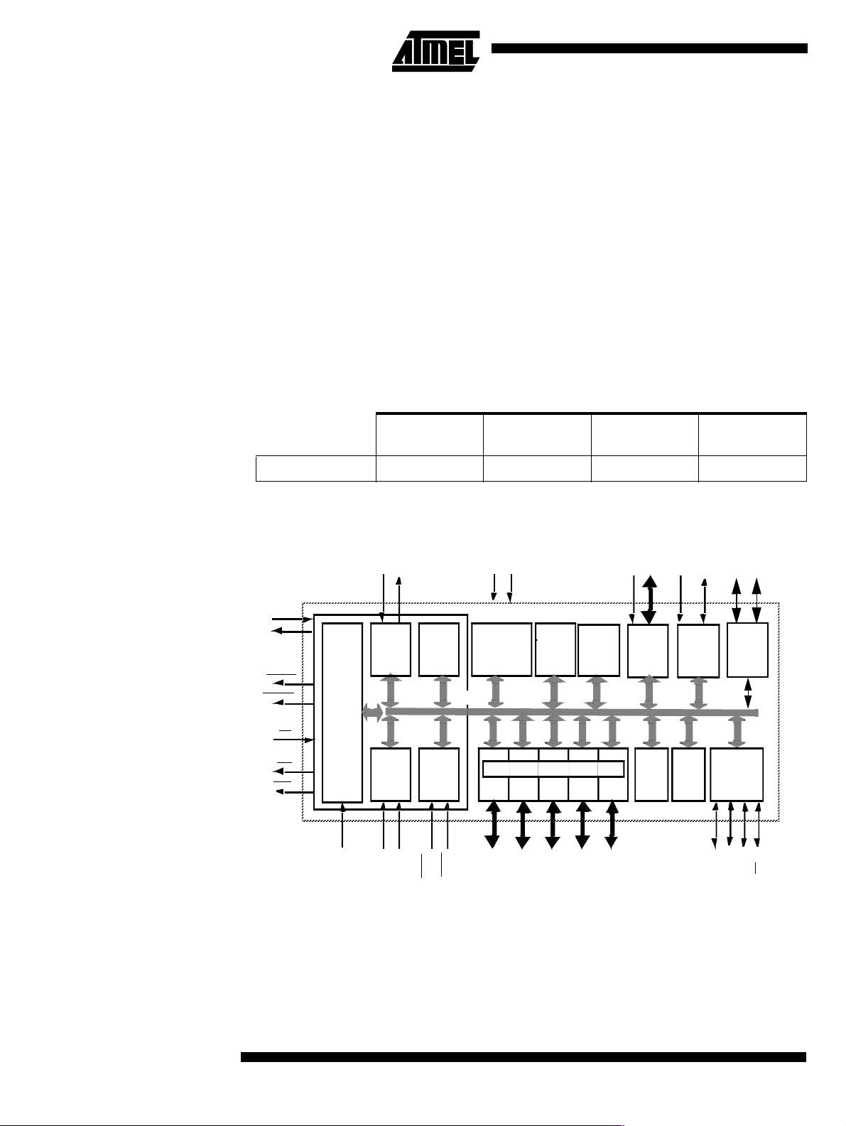
Block Diagram
ALE/
XTAL1
XTAL2
PRO G
PSEN
EA
RD
WR
PLCC44
VQFP441.4 Flash(bytes) XRAM (bytes)
TOTALRAM
(bytes) I/O
T89C51IC2 32k 1024 1280 34
CC
Vss
V
Flash
32K x8 or
16Kx8
IB-bus
Parallel I/O Ports & Ext. Bus
Port0
XRAM
1Kx8
Port 1 Port 2 Port 3
Boot
ROM
2Kx8
PortI2
(1)
ECI
PCA
Watch
Dog
PCA
(1)
T2EX
(1) (1)
Timer2
Key
Board
T2
SPI
(1) (1) (1)
SDA
(2)
(2)
CPU
RxD
TxD
(2)(2)
EUART
BRG
Timer 0
Timer 1
(2) (2) (2) ( 2 )
RAM
+
256x8
C51
CORE
INT
Ctrl
SCL
I2C
(1)
P0
P1
P2
T0
T1
RESET
2
T89C51IC2
INT1
INT0
(1): A l ternatefunctionof Port 1
(2): Alternatefunction of Port3
P3
PI2
MISO
MOSI
SCK
SS
Rev. C – 3-Dec-01
Page 3

SFR Mapping
T89C51IC2
The Special Function Registers (SFRs) of the T89C51IC2 fall into the following
categories:
• C51 core registers: ACC, B, DPH, DPL, P S W, SP
• I/O port registers: P0, P 1, P2, P3, PI2
• Timer registers: T2CON, T2MOD, TCON, TH0, TH1, TH2, TMOD, TL0, TL1, TL2,
RCAP2L, RCAP2H
• Serial I/O port registers: SADDR, SADEN, SBUF, SCON
• PCA (Programmable Counter Array) registers: CCON, CCAP Mx, CL, CH, CCA PxH,
CCAPxL(x:0to4)
• Power and clock control registers: PCON
• Hardware Watchdog Timer registers: WDTRST, WDTPRG
• Interrupt system registers: IE0, IPL0, IPH0, IE1, IPL1, IPH1
• Keyboard Interface registers: KBE, KBF, KBLS
• SPI registers: SPCON, SPSTR, SPDAT
• I2C Interface registers: SSCON, SSCS, SSDAT, SSADR
• BRG (Baud Rate Generator) registers: BRL, BDRCON
• Flash register: FCON
• Clock Prescaler register: CKRL
• 32Khz Sub Clock Oscillator registers: CKSEL, OSSCON
• Others: AUXR, AUXR1, CKCON0, CKCON1
Rev. C – 3-Dec-01
3
Page 4

F8h
F0h
E8h
Table 2. SF R mapping
Table below shows all SFRs with their address and their reset value.
Bit
addressable
0/8 1/9 2/A 3/B 4/C 5/D 6/E 7/F
CH
0000 0000
B
0000 0000
CL
0000 0000
CCAP0H
XXXX XXXX
CCAP0L
XXXX XXXX
CCAP1H
XXXX XXXX
CCAP1L
XXXX XXXX
Non Bit addressable
CCAPL2H
XXXX XXXX
CCAPL2L
XXXX XXXX
CCAPL3H
XXXX XXXX
CCAPL3L
XXXX XXXX
CCAPL4H
XXXX XXXX
CCAPL4L
XXXX XXXX
FFh
F7h
EFh
E0h
D8h
D0h
C8h
C0h
B8h
B0h
A8h
A0h
98h
90h
88h
80h
ACC
0000 0000
CCON
00X0 0000
PSW
0000 0000
T2CON
0000 0000
PI2 bit
addressable
XXXX XX11
IPL0
X000 000
P3
1111 1111
IE0
0000 0000
P2
1111 1111
SCON
0000 0000
P1
1111 1111
TCON
0000 0000
P0
1111 1111
0/8 1/9 2/A 3/B 4/C 5/D 6/E 7/F
CMOD
00XX X000
FCON (1)
XXXX 0000
T2MOD
XXXX XX00
SADEN
0000 0000
IE1
XXXX X000
SADDR
0000 0000
SBUF
XXXX XXXX
TMOD
0000 0000
SP
0000 0111
CCAPM0
X000 0000
RCAP2L
0000 0000
IPL1
XXXX X000
AUXR1
XXXX X0X0
BRL
0000 0000
TL0
0000 0000
DPL
0000 0000
CCAPM1
X000 0000
RCAP2H
0000 0000
SPCON
0001 0100
IPH1
XXXX X111
BDRCON
XXX0 0000
SSCON
0000 0000
TL1
0000 0000
DPH
0000 0000
CCAPM2
X000 0000
TL2
0000 0000
SPSTA
0000 0000
KBLS
0000 0000
SSCS
1111 1000
TH0
0000 0000
CCAPM3
X000 0000
TH2
0000 0000
SPDAT
XXXX XXXX
KBE
0000 0000
SSDAT
1111 1111
TH1
0000 0000
CKSEL
XXXX XXX0
CCAPM4
X000 0000
WDTRST
XXXX XXXX
KBF
0000 0000
SSADR
1111 1110
AUXR
XX0X 0000
OSSCON
XXXX X001
IPH0
X000 0000
CKCON1
XXXX XXX0
WDTPRG
XXXX X000
CKRL
1111 1111
CKCON0
0000 0000
PCON
00X1 0000
E7h
DFh
D7h
CFh
C7h
BFh
B7h
AFh
A7h
9Fh
97h
8Fh
87h
reserved
(1) FCON access is reserved for the FLASH API and ISP software.
4
T89C51IC2
Rev. C – 3-Dec-01
Page 5

Pin Configurations
T89C51IC2
P1.5/CEX2/MISO
P1.6/CEX3/SCK
P1.7/CEx4/MOSI
RST
P3.0/RxD
PI2.1/SDA
P3.1/TxD
P3.2/INT0
P3.3/INT1
P3.4/T0
P3.5/T1
P1.4/CEX1
P1.3/CEX0
543216
7
8
9
10
11
12
13
14
15
16
17
P1.1/T2EX/SS
P1.2/ECI
P1.0/T2/XTALB1
XTALB2
VCC
44 43 42 41 40
PLCC44
P0.0/AD0
18 19 23222120 262524 2728
NIC*
VSS
XTAL2
XTAL1
P3.7/RD
P3.6/WR
P2.0/A8
P2.1/A9
P0.1/AD1
P2.2/A10
P0.2/AD2
P2.3/A11
P0.3/AD3
39
38
37
36
35
34
33
32
31
30
29
P2.4/A12
P0.4/AD4
P0.5/AD5
P0.6/AD6
P0.7/AD7
EA
PI2.0/SCL
ALE/PROG
PSEN
P2.7/A15
P2.6/A14
P2.5/A13
Rev. C – 3-Dec-01
P1.5/CEX2/MISO
P1.6/CEX3/SCK
P1.7/CEX4/MOSI
RST
P3.0/RxD
PI2.1/SDA
P3.1/TxD
P3.2/INT0
P3.3/INT1
P3.4/T0
P3.5/T1
P1.4/CEX1
43 42 41 40 3944 38 37 36 35 34
1
2
3
4
5
6
7
8
9
10
11
P1.1/T2EX/SS
P1.3/CEX0
P1.2/ECI
VQFP44 1.4
P1.0/T2/XTALB1
XTA LB2
VCC
P0.0/AD0
1213 17161514 201918 2122
VSS
NIC*
XTA L1
XTAL2
P3.7/RD
P3.6/WR
P2.0/A8
P2.1/A9
P0.2/AD2
P0.3/AD3
P0.1/AD1
P0.4/AD4
33
32
P0.5/AD5
31
P0.6/AD6
30
P0.7/AD7
29
EA
28
PI2.0/SCL
27
ALE/PROG
26
PSEN
25
P2.7/A15
24
P2.6/A14
23
P2.5/A13
P2.3/A1 1
P2.2/A10
P2.4/A12
5
Page 6

Table 1. Pin Description for 40/44 pin packages
Pin Number
Mnemonic
V
SS
V
CC
P0.0-P0.7 43-36 37-30 I/O Port 0: Port 0 is an open-drain, bidirectional I/O port. Port 0 pins that have 1s written to
P1.0-P1.7 2-9 40-44
22 16 I Ground: 0V reference
44 38 I
1-3
240I/OP1.0: Input / Output
341I/OP1.1: Input / Output
Type
Name and FunctionPLCC44 VQFP44 1.4
Power Supply: This is the power supply voltage for normal, idle and power-down
operation
them floata nd can be used as high impedance inputs. Port0 must be polarized to V
or VSSin order to prevent any parasitic current consumption. Port 0 is also the
multiplexed low-orderaddress and databus duringaccess to external program and
datamemory. In this application, it usesstrong internal pull-upwhenemitting 1s.Port 0
alsoinputsthe codebytes during EPROM programming.Externalpull-ups arerequired
duringprogram verification duringwhich P0 outputs the codebytes.
I/O Port 1: Port 1 is an 8-bit bidirectional I/O portwith internalpull-ups.Port1pinsthat
have 1s written to them are pulled high by the internal pull-ups and can be used as
inputs. As inputs,Port 1 pins thatare externallypulled low will sourcecurrent because
of the internal pull-ups.Port 1 also receives the low-orderaddress byteduri ng memory
programming and verification.
Alternate functions for T89C51IC2 Port 1 include:
I/O T2 (P1.0): Timer/Counter2external count input/Clockout
I XTALB1 (P1.0): Sub Clock input to the inverting oscillator amplifier
CC
I T2EX: Timer/Counter 2 Reload/Capture/Direction Control
I SS
442I/OP1.2: Input / Output
I ECI: External Clockforthe PCA
543I/OP1.3: Input / Output
I/O CEX0: Capture/Compare External I/O for PCA module 0
644I/OP1.4: Input / Output
I/O CEX1: Capture/Compare External I/O for PCA module 1
71I/OP1.5: Input / Output
I/O CEX2: Capture/Compare External I/O for PCA module 2
I/O MISO: SPI Master Input Slave Output line
82I/OP1.6: Input / Output
I/O CEX3: Capture/Compare External I/O for PCA module 3
I/O SCK: SPI Serial Clock
: SPI Slave Select
When SPIis in master mode,MISO receives data fromtheslave peripheral. When SPI
is in slave mode, MISO outputs data to the master controller.
SCK outputsclock to the slaveperipheral
93I/OP1.7: Input / Output:
6
T89C51IC2
Rev. C – 3-Dec-01
Page 7

T89C51IC2
Pin Number
Mnemonic
XTALA1 21 15 I
XTALA2 20 14 O Crystal A 2: Output from the inverting oscillatoramplifier
XTALB1 2 40 I
XTALB2 1 39 O Crystal B 2: (Sub Clock) Output from the inverting oscillator amplifier
P2.0-P2.7 24-31 18-25 I/O Port 2: Port 2 is an 8-bit bidirectional I/O port withinternalpull-ups.Port 2 pins that
Type
Name and FunctionPLCC44 VQFP44 1.4
I/O CEX4: Capture/Compare External I/O for PCA module 4
I/O MOSI: SPI Master Output Slave Input line
When SPI is in mastermode, MOSI outputsdata to the slave peripheral. When SPI is
in slave mode, MOSI receives data from the master controller.
Crystal A 1: Input to the inverting oscillator amplifier and inputto the internalclock
generator circuits.
Crystal B 1: (Sub Clock) Input to the inverting oscillator amplifier and input to the
internal clockgenerator circuits.
have 1s written to them are pulled high by the internal pull-ups and can be used as
inputs. As inputs,Port 2 pins thatare externallypulled low will sourcecurrent because
of the internal pull-ups. Port 2 emits the high-order addressbyte duringfetches from
external programmemoryand duringaccessestoexternaldata memorythatuse 16-bit
addresses (MOVX@DPTR).In this application, it usesstrong internal pull-ups emitting
1s. During accesses to external data memory that use 8-bit addresses (MOVX @Ri),
port 2 emitsthecont ents of the P2 SFR. Some Port 2 pins receive the highorder
addressbits duringEPROM programming and verification:
P2.0 to P2.5 for 16Kb devices
P2.0 to P2.6 for 32Kb devices
P3.0-P3.7 11,
13-19
11 5 I RXD (P3.0): Serialinput port
13 7 O TXD (P3.1): Serial outputport
14 8 I INT0
15 9 I INT1
16 10 I T0 (P3.4): Timer0external input
17 11 I T1 (P3.5): Timer1external input
18 12 O WR
19 13 O RD
PI2.0-PI2.1
34, 12 28, 6
34 28 I/O SCL (PI2.0): I2C Serial Clock
12 6 I/O SDA (PI2.1): I2CSerial Data
5,
7-13
I/O Port 3: Port 3 is an 8-bit bidirectional I/O portwith internalpull-ups.Port3pinsthat
have 1s written to them are pulled high by the internal pull-ups and can be used as
inputs. As inputs,Port 3 pins thatare externallypulled low will sourcecurrent because
of the internal pull-ups. Port 3 also serves the special features of the 80C51 family, as
listedbelow.
(P3.2): External interrupt 0
(P3.3): External interrupt 1
(P3.6): External data memory writestrobe
(P3.7): Externaldata memoryreadstrobe
Port I2: Port I2 is an open drain.It can be used as inputs (must be polarized to Vcc
with external resistor to prevent any parasitic current consumption).
SCL outputtheserial clocktoslave peripherals
SCL input the serial clock from master
Rev. C – 3-Dec-01
SDA is the bidirectional I2C data line
7
Page 8

Pin Number
Type
Mnemonic
RST 10 4 I/O
Name and FunctionPLCC44 VQFP44 1.4
Reset: A high on this pin for two machine cycles while the oscillator is running, resets
the device. An internaldiffusedresistor to V
external capacitor to V
system reset.
. This pin is an output when the hardware watchdog forces a
CC
permits a power-on reset using only an
SS
ALE/PROG
PSEN 32 26 O Program StrobeENable: The read strobe to external program memory. When
EA 35 29 I External Access Enable: EA
33 27 O (I) Address Latch Enable/Program Pulse:Output pulse for latching t he low byte of the
address during an access to external memory. In normal operation, ALE is emitted at a
constant rate of 1/6 (1/3 in X2 mode) the oscillator frequency, and can be used for
external timing or clocking. Note that one ALE pulse is skipped during each access to
external data memory.This pin is also theprogram pulse input (PROG
programming. ALE can be disabled by setting SFR’s AUXR.0 bit. With this bit set, ALE
will be inactive during internalfetches.
executing code from the external program memory, PSEN
machinecycle, exceptthattwo PSEN
external data memory.PSE N
memory.
codefrom externalprogram memorylocations0000HtoFFFFH(RD). Ifsecuritylevel 1
is programmed, EA
willbeinternally latchedonReset.
is not activated duringfetches from internal program
activations are skipped duringeachaccess to
mustbeexternally held low to enable the device tofetch
is activated twice each
) during Flash
8
T89C51IC2
Rev. C – 3-Dec-01
Page 9

Ordering Information
T89C51IC2
Table 2. Possible order entries
Flash
Memory
Part Number
T89C51IC2-SLSCM 32 Kbytes 5 V Commercial 20 MHz PLCC44 Stick
T89C51IC2-SLSIM 32 Kbytes 5V Industrial 20 MHz PLCC44 Stick
T89C51IC2-SLSIL 32 Kbytes 3V Industrial 20MHz PLCC44 Stick
T89C51IC2-RLTIM 32 Kbytes 5V Industrial 20 MHz VQFP44 Tray
T89C51IC2-RLTIL 32 Kbytes 3V Commercial 20 MHz VQFP44 Tray
Size
Supply
Voltage
Temperature
Range
Max
Frequency Package Packing
Rev. C – 3-Dec-01
Note: Purchaseof Atmel I2C components conveys a license under the PhilipsI2C Patent’s right
to use these components in an I
2
C system, provided that the system conforms to the I2C
Standard Specification as defined by Phi lips.
9
Page 10

Atmel Sales Offices
France
3, Avenue du Centre
78054 St.-Quentin-en-Yvelines
Cedex
France
Tel: 33130 60 70 00
Fax: 33130 60 71 11
Germany
Erfurt er S t ras se 3 1
85386 Eching
Germany
Tel: 49893 19 70 0
Fax: 49893 19 46 21
Kruppstrasse 6
45128 Essen
Germany
Tel: 492 012 47 30 0
Fax: 492 012 47 30 47
Theresienstrasse 2
74072 Heilbronn
Germany
Tel: 4971 3167 36 36
Fax: 4971 3167 31 63
Italy
Via Grosio, 10/8
20151 Milano
Italy
Tel: 390238037-1
Fax: 390238037-234
Spain
Principe de Vergara, 112
28002 Madrid
Spain
Tel: 3491564 51 81
Fax: 3491562 75 14
Sweden
Kavallerivaegen 24, Rissne
17402 Sundbyberg
Sweden
Tel: 468587 48 800
Fax: 468587 48 850
United Kingdom
Easthampstead Road
Bracknell, Berkshire RG12 1LX
United K ingdom
Tel: 441344707 300
Fax: 441344427 371
USA
2325 Orchard Parkway
San Jose
California 95131
USA-Calif ornia
Tel: 1408441 0311
Fax: 1408436 4200
1465 Route 31, 5th Floor
Annandale
New Jersey 08801
USA-New Je rsey
Tel: 1908848 5208
Fax: 1908848 5232
Hong Kong
77 Mody Rd., Tsimshatsui East,
Rm.1219
East Kowloon
Hong Kong
Tel: 85223789 789
Fax: 85223755 733
Korea
Ste.605,Sings ong Bldg. Youngdeungpo-ku
150-010 Seoul
Korea
Tel: 8227851136
Fax: 8227851137
Singapore
25 Tampines Street 92
Singapore 528877
Rep. of Singapore
Tel: 65260 8223
Fax: 65787 9819
Taiwan
WenHwa2Road,LinKou
Hsiang
244 Taipei Hsien 244
Taiwan, R.O.C.
Tel: 88622609 5581
Fax: 88622600 2735
Japan
1-24-8 Shinkawa, Chuo-Ku
104-0033 Tokyo
Japan
Tel: 8133523 3551
Fax: 8133523 7581
Web site
http://ww w.a tmel- wm .com
© Atmel Na ntes SA, 2001 .
Atmel C or p or ation makes no w arrant y for the u se of its pr oducts, o ther than those expres sl y c ontaine d in the Com pany’s standard warranty
which is detailed in Atmel’s Terms and Conditions located on the Company’s web site. The Company assumes no responsibility for any errors
which may appear in this document, reserves the right to change devices or specificat ions detailed herein at any time without notice, and does
not make any commitment to update the information contained herein. No licenses to patents or other intellectual property of Atmel are granted
by t he Company in connec tion w ith the sale of A tmel prod uc ts, expressly or by impl ication . Atmel’s product s are not autho r iz ed for use as critic al
components in life support devices or systems.
Printedonrecycledpaper.
 Loading...