

Page 1

8-bit MCU with CAN controller and Flash
1. Description
T89C51CC02
Part of the CANaryTMfamily of microcontrollers
dedicated to CAN network applications, the
T89C51CC02 is a low pin count 8-bit Flash
microcontroller.
While remaining fully compatible with the 80C51 it
offers a superset of this standard microcontroller. In X2
mode a maximum external clock rate of 20 MHz reaches
a 300 ns cycle time.
2. Features
• 80C51 core architecture:
• 256 bytes of on-chip RAM
• 256 bytes of on-chip ERAM
• 16 Kbytes of on-chip Flash memory
Read/Write cycle : 10k
Data Retention 10 years at 85°C
• 2 Kbytes of on-chip Flash for Bootloader
• 2 Kbytes of on-chip EEPROM
Read/Write cycle : 100k
• 14-source 4-level interrupt
• Three 16-bit timer/counter
• Full duplex UART compatible 80C51
• maximum crystal frequency 40 MHz. In X2 mode,
20 MHz (CPU core, 40 MHz)
• three or four ports: 16 or 20 digital I/O lines
• two-channel 16-bit PCA with:
- PWM (8-bit)
- High-speed output
- Timer and edge capture
• Double Data Pointer
• 21-bit watchdog timer (including 7 programmable
bits)
• A 10-bit resolution analog to digital converter (ADC)
with 8 multiplexed inputs
• Separate power supply for analog
• Full CAN controller:
• Fully compliant with CAN standard rev 2.0 A
and 2.0 B
• Optimized structure for communication
management (via SFR)
• 4 independent message objects:
- Each message object programmable on
transmission or reception
Besides the full CAN controller T89C51CC02 provides
16 Kbytes of Flash memory including In-system
Programming (ISP), 2-Kbyte Boot Flash Memory, 2Kbyte EEPROM and 512 bytes RAM.
Special attention is payed to the reduction of the electromagnetic emission of T89C51CC02.
- individual tag and mask filters up to 29-bit
identifier/message object
- 8-byte cyclic data register (FIFO)/message
object
- 16-bit status & control register/message object
- 16-bit Time-Stamping register/message object
- CAN specification 2.0 part A or 2.0 part B
programmable message objects
- Access to message object control and data
register via SFR
- Programmable reception buffer lenght up to
4 message objects
- Priority management of reception of hits on
several message objects at the same time
(Basic CAN Feature)
- Priority management for transmission
- message object overrun interrupt
• Supports
- Time Triggered Communication.
- Autobaud and Listening mode
- Automatic reply mode programmable
• 1 Mbit/s maximum transfer rate at 8MHz* Crystal
frequency in X2 mode.
• Readable error counters
• Programmable link to on-chip Timer for Time
Stamping and Network synchronization
• Independent baud rate prescaler
• Data, Remote, Error and overload frame handling
• Power saving modes:
• Idle mode
• Power down mode
• Power supply: 5V +/- 10% ,3V +/- 10%
• Temperature range: Industrial (-40° to +85°C)
• Packages: PLCC28, SOIC28, (TSSOP28, SOIC24)**
Rev.A- May 17, 2001 1
Preliminary
Page 2
T89C51CC02
* At BRP = 1 sampling point will be fixed.
** Ask for availability
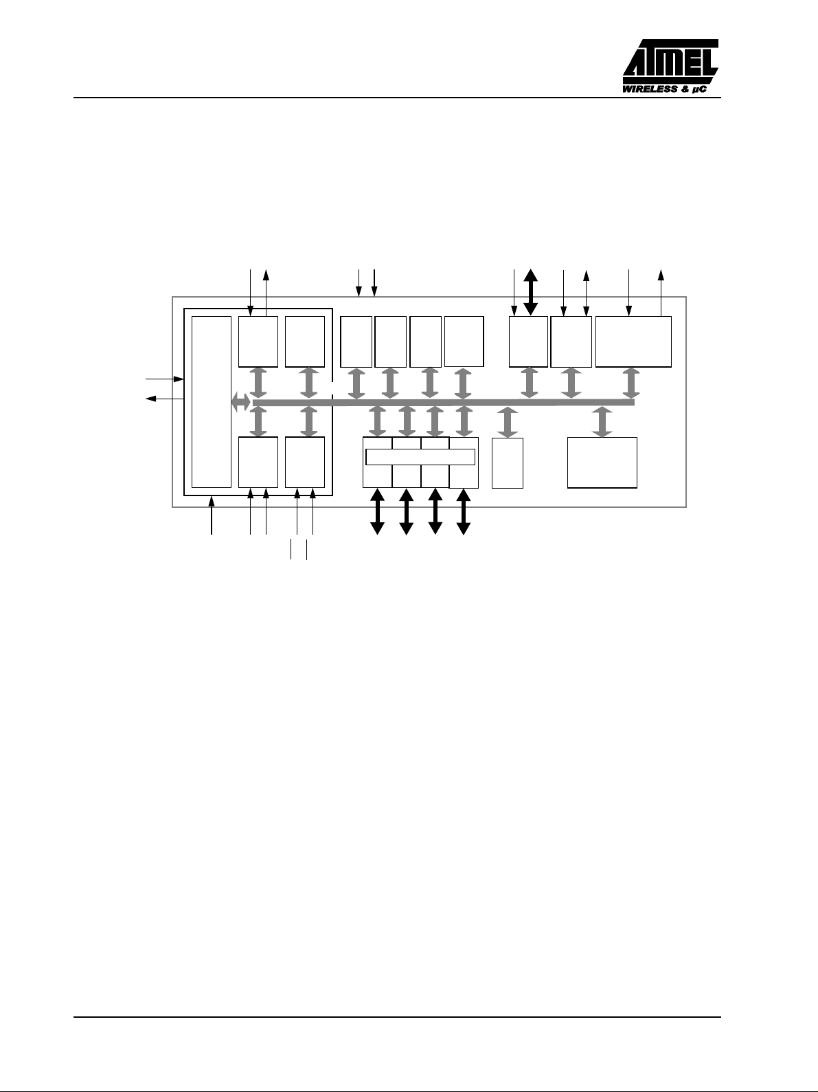
3. Block Diagram
RxD
TxD
Vcc
Vss
ECI
PCA
T2EX
T2
RxDC
TxDC
XTAL1
XTAL2
CPU
RESET
UART
Timer 0
Timer 1
T0
C51
CORE
T1
RAM
256x8
INT
Ctrl
INT0
Flash
Boot
16kx
loader
8
IB-bus
Port 1
INT1
(1): 8 analog Inputs / 8 Digital I/O
(2): 2-Bit I/O Port
PROM
2kx8
Parallel I/O Ports & Ext. Bus
Port 2
P1(1)
P2(2)
EE
2kx8
Port 3
P3
ERAM
256x8
Port 4
P4(2)
Watch
Dog
PCA
Timer2
CAN
CONTROLLER
10 bit
ADC
2 Rev.A - May 17, 2001
Preliminary
Page 3
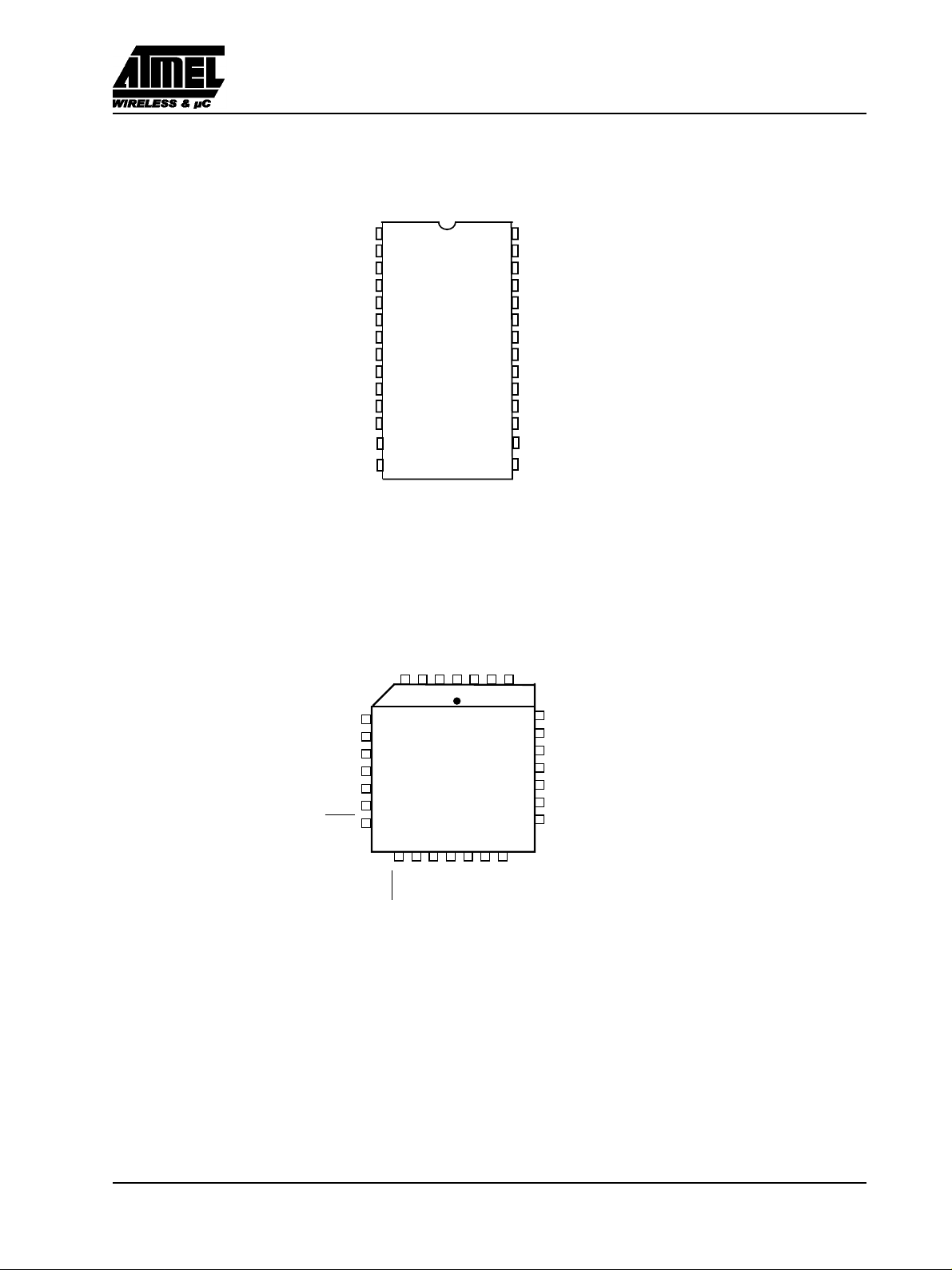
4. Pin Configuration
T89C51CC02
VAREF
VAGND
VAVCC
P4.1/RxDC
P4.0/TxDC
P3.5/T1
P3.4/T0
P3.3/INT1
P3.2/INT0
P3.1/TxD
P3.0/RxD
P4.0/ TxDC
P2.1
P3.7
P3.6
P3.5 / T1
P3.4 / T0
P3.3 / INT1
P2.1
P3.7
P3.6
1
2
3
4
5
6
7
SO28
8
9
10
11
12
13
14
VAGND
P4.1 / TxDC
VAVCC
432
5
6
7
8
PLCC-28
9
10
11
12131415161718
28
27
26
25
24
23
22
21
20
19
18
17
16
15
P1.2 / AN2 / ECI
P1.1 / AN1 / T2EX
P1.0 / AN 0 / T2
VAREF
1
282726
25
24
23
22
21
20
19
P1.0/
AN0/T2
P1.1/AN1/T2EX
P1.2/AN2/ECI
P1.3/AN3/CEX0
P1.4/AN4/CEX1
P1.5/AN5
P1.6/AN6
P1.7/AN7
P2.0
RESE
T
VSS
VCC
XTAL1
XTAL2
P1.3 / AN3 / CEX0
P1.4 / AN4 / CEX1
P1.5 / AN5
P1.6 / AN6
P1.7 / AN7
P2.0
RESET
VSS
VCC
XTAL1
XTAL2
P3.1 / TxD
P3.0 / RxD
P3.2 / INT0
Rev.A - May 17, 2001 3
Preliminary
Page 4

T89C51CC02
Table 1. Pin Description
Pin Name Type Description
VSS GND Circuit ground potential.
VCC Supply voltage during normal, idle, and power-down operation.
VAREF Reference Voltage for ADC
VAVCC Supply Voltage for ADC
VAGND Reference Ground for ADC / Analog Ground
Port 1:
is an 8-bit bi-directional I/O port with internal pull-ups. Port 1 pins can be used for digital input/output
or as analog inputs for the Analog Digital Converter (ADC). Port 1 pins that have 1’s written to them
are pulled high by the internal pull-up transistors and can be used as inputs in this state. As inputs, Port
1 pins that are being pulled low externally will be the source of current (IIL, on the datasheet) because
of the internal pull-ups. Port 1 pins are assigned to be used as analog inputs via the ADCF register.
As a secondary digital function, port 1 contains the Timer 2 external trigger and clock input; the PCA
external clock input and the PCA module I/O.
P1.0:7 I/O
P2.0:1 I/O
P3.0:7 I/O
P1.0 / AN0 / T2
Analog input channel 0,
External clock input for Timer/counter2.
P1.1 / AN1 / T2EX
Analog input channel 1,
Trigger input for Timer/counter2.
P1.2 / AN2 / ECI
Analog input channel 2,
PCA external clock input.
PIn the T89C51CC02 Port 1 can sink or source 5mA. It can drive CMOS inputs without external pull-ups.
Port 2:
Is an 2-bit bi-directional I/O port with internal pull-ups. Port 2 pins that have 1’s written to them are
pulled high by the internal pull-ups and can be used as inputs in this state. As inputs, Port 2 pins that
are being pulled low externally will be a source of current (IIL, on the datasheet) because of the internal
pull-ups.
In the T89C51CC02 Port 2 can sink or source 5mA. It can drive CMOS inputs without external pull-ups.
Port 3:
Is an 8-bit bi-directional I/O port with internal pull-ups. Port 3 pins that have 1’s written to them are
pulled high by the internal pull-up transistors and can be used as inputs in this state. As inputs, Port 3
pins that are being pulled low externally will be a source of current (IIL, on the datasheet) because of the
internal pull-ups.
The output latch corresponding to a secondary function must be programmed to one for that function to
operate. The secondary functions are assigned to the pins of port 3 as follows:
P3.0 / RxD:
Receiver data input (asynchronous) or data input/output (synchronous) of the serial interface
P3.1 / TxD:
Transmitter data output (asynchronous) or clock output (synchronous) of the serial interface
P3.2 / INT0:
External interrupt 0 input / timer 0 gate control input
P3.3 / INT1:
External interrupt 1 input / timer 1 gate control input
P3.4 / T0:
Timer 0 counter input
P3.5 / T1:
Timer 1 counter input
P3.6
P3.7
In the T89C51CC02 Port 3 can sink or source 5mA. It can drive CMOS inputs without external pull-ups.
4 Rev.A - May 17, 2001
Preliminary
Page 5

Pin Name Type Description
Port 4:
Is an 2-bit bi-directional I/O port with internal pull-ups. Port 4 pins that have 1’s written to them are
pulled high by the internal pull-ups and can be used as inputs in this state. As inputs, Port 4 pins that are
being pulled low externally will be a source of current (IIL, on the datasheet) because of the internal pullup transistor.
The output latch corresponding to a secondary function RxDC must be programmed to one for that function
P4.0:1 I/O
RESET I/O
XTAL1 I
XTAL2 O
to operate. The secondary functions are assigned to the two pins of port 4 as follows:
P4.0 / TxDC:
Transmitter output of CAN controller
P4.1 / RxDC:
Receiver input of CAN controller.
In the T89C51CC02 Port 4 can sink or source 5mA. It can drive CMOS inputs without external pull-ups.
Reset:
A high level on this pin during two machine cycles while the oscillator is running resets the device. An
internal pull-down resistor to VSS permits power-on reset using only an external capacitor to VCC.
XTAL1:
Input of the inverting oscillator amplifier and input of the internal clock generator circuits.
To drive the device from an external clock source, XTAL1 should be driven, while XTAL2 is left
unconnected. To operate above a frequency of 16 MHz, a duty cycle of 50% should be maintained.
XTAL2:
Output from the inverting oscillator amplifier.
T89C51CC02
Rev.A - May 17, 2001 5
Preliminary
Page 6
T89C51CC02
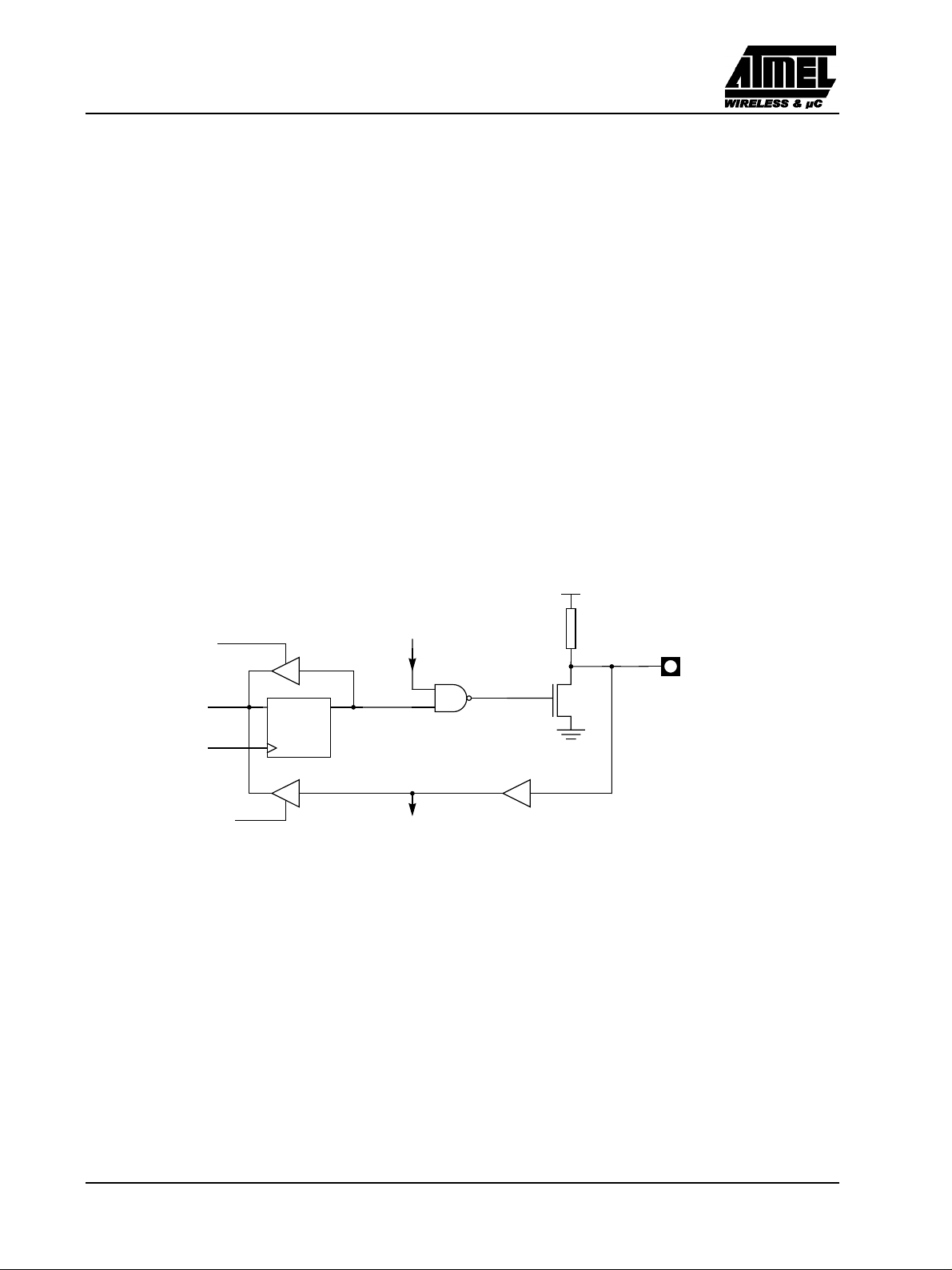
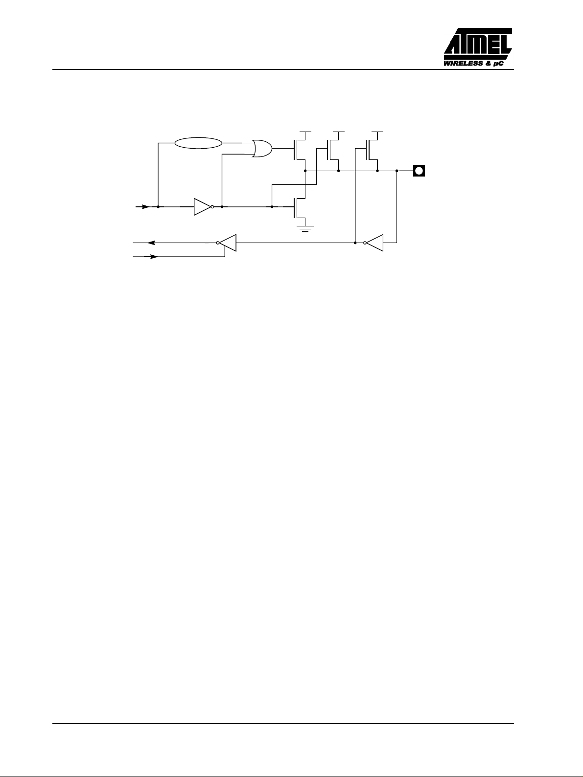
4.1. I/O Configurations
Each Port SFR operates via type-D latches, as illustrated in Figure 1 for Ports 3 and 4. A CPU "write to latch"
signal initiates transfer of internal bus data into the type-D latch. A CPU "read latch" signal transfers the latched
Q output onto the internal bus. Similarly, a "read pin" signal transfers the logical level of the Port pin. Some Port
data instructions activate the "read latch" signal while others activate the "read pin" signal. Latch instructions are
referred to as Read-Modify-Write instructions. Each I/O line may be independently programmed as input or output.
4.2. Port Structure
Figure 1 shows the structure of Ports 1 and 3, which have internal pull-ups. An external source can pull the pin
low. Each Port pin can be configured either forgeneral-purpose I/O or for its alternate input output function.
To use a pin for general-purpose output, set or clear the corresponding bit in the Px register (x=1,3 or 4). To use
a pin for general purpose input, set the bit in the Px register. This turns off the output FET drive.
To configure a pin for its alternate function, set the bit in the Px register. When the latch is set, the "alternate
output function" signal controls the output level (see Figure 1). The operation of Ports 1, 3 and 4 is discussed
further in "quasi-Bidirectional Port Operation" paragraph.
ALTERNATE
OUTPUT
READ
LATCH
INTERNAL
BUS
WRITE
TO
LATCH
READ
PIN
NOTE:
1. The internal pull-up can be disabled on P1 when analog function is selected.
D
CL
Port.X
LATCH
Q
FUNCTION
ALTERNATE
INPUT
FUNCTION
Figure 1. Port Structure
VCC
INTERNAL
PULL-UP (1)
Port.x
6 Rev.A - May 17, 2001
Preliminary
Page 7
T89C51CC02
4.3. Read-Modify-Write Instructions
Some instructions read the latch data rather than the pin data. The latch based instructions read the data, modify
the data and then rewrite the latch. These are called "Read-Modifiy-Write" instructions. Below is a complete list
of these special instructions (see Table 2). When the destination operand is a Port or a Port bit, these instructions
read the latch rather than the pin:
Table 2. Read-Modify-Write Instructions
Instruction Description Example
ANL logical AND ANL P1, A
ORL logical OR ORL P2, A
XRL logical EX-OR XRL P3, A
JBC jump if bit = 1 and clear bit JBC P1.1, LABEL
CPL complement bit CPL P3.0
INC increment INC P2
DEC decrement DEC P2
DJNZ decrement and jump if not zero DJNZ P3, LABEL
MOV Px.y, C move carry bit to bit y of Port x MOV P1.5, C
CLR Px.y clear bit y of Port x CLR P2.4
SET Px.y set bit y of Port x SET P3.3
It is not obvious the last three instructions in this list are Read-Modify-Write instructions. These instructions read
the port (all 8 bits), modify the specifically addressed bit and write the new byte back to the latch. These ReadModify-Write instructions are directed to the latch rather than the pin in order to avoid possible misinterpretation
of voltage (and therefore, logic)levels at the pin. For example, a Port bit used to drive the base of an external
bipolar transistor can not rise above the transistor’s base-emitter junction voltage (a value lower than VIL). With
a logic one written to the bit, attemps by the CPU to read the Port at the pin are misinterpreted as logic zero. A
read of the latch rather than the pins returns the correct logic-one value.
4.4. Quasi-Bidirectional Port Operation
Port 1, Port 3 and Port 4 have fixed internal pull-ups and are referred to as "quasi-bidirectional" Ports. When
configured as an input, the pin impedance appears as logic one and sources current in response to an external logic
zero condition. Resets write logic one to all Port latches. If logical zero is subsequently written to a Port latch, it
can be returned to input condions by a logical one written to the latch.
NOTE:
Port latch values change near the end of Read-Modify-Write insruction cycles. Output buffers (and therefore the pin state) update early in the
instruction after Read-Modify-Write instruction cycle.
Logical zero-to-one transitions in Port 1, Port 3 and Port 4 use an additional pull-up (p1) to aid this logic transition
see Figure. This increases switch speed. This extra pull-up sources 100 times normal internal circuit current during
2 oscillator clock periods. The internal pull-ups are field-effect transistors rather than linear resistors. Pull-ups
consist of three p-channel FET (pFET) devices. A pFET is on when the gate senses logical zero and off when the
gate senses logical one. pFET #1 is turned on for two oscillator periods immediately after a zero-to-one transition
in the Port latch. A logical one at the Port pin turns on pFET #3 (a weak pull-up) through the inverter. This
inverter and pFET pair form a latch to drive logical one. pFET #2 is a very weak pull-up switched on whenever
the associated nFET is switched off. This is traditional CMOS switch convention. Current strengths are 1/10 that
of pFET #3.
Rev.A - May 17, 2001 7
Preliminary
Page 8
T89C51CC02
OUTPUT DATA
INPUT DATA
READ PIN
2 Osc. PERIODS
p1
p2
n
Figure 2. Internal Pull-Up Configurations
VCCVCCVCC
p3
P1.x
P2.x
P3.x
P4.x
8 Rev.A - May 17, 2001
Preliminary
Page 9
T89C51CC02
5. SFR Mapping
The Special Function Registers (SFRs) of the T89C51CC02 fall into the following categories:
Table 3. C51 Core SFRs
Mnemonic Add Name 7 6 5 4 3 2 1 0
ACC E0h Accumulator
B F0h B Register
PSW D0h Program Status Word
SP 81h
DPL 82h
DPH 83h
Mnemonic Add Name 7 6 5 4 3 2 1 0
P1 90h Port 1
P2 A0h Port 2 (x2)
P3 B0h Port 3
P4 C0h Port 4 (x2)
Stack Pointer
LSB of SPX
Data Pointer Low byte
LSB of DPTR
Data Pointer High byte
MSB of DPTR
Table 4. I/O Port SFRs
Table 5. Timers SFRs
Mnemonic Add Name 7 6 5 4 3 2 1 0
TH0 8Ch Timer/Counter 0 High byte
TL0 8Ah Timer/Counter 0 Low byte
TH1 8Dh Timer/Counter 1 High byte
TL1 8Bh Timer/Counter 1 Low byte
TH2 CDh Timer/Counter 2 High byte
TL2 CCh Timer/Counter 2 Low byte
TCON 88h Timer/Counter 0 and 1 control
TMOD 89h Timer/Counter 0 and 1 Modes
T2CON C8h Timer/Counter 2 control
T2MOD C9h Timer/Counter 2 Mode
RCAP2H CBh
RCAP2L CAh
WDTRST A6h WatchDog Timer Reset
WDTPRG A7h WatchDog Timer Program
Timer/Counter 2 Reload/Capture
High byte
Timer/Counter 2 Reload/Capture
Low byte
TF1 TR1 TF0 TR0 IE1 IT1 IE0 IT0
GATE1 C/T1# M11 M01 GATE0 C/T0# M10 M00
TF2 EXF2 RCLK TCLK EXEN2 TR2 C/T2# CP/RL2#
- - - - - - T2OE DCEN
-----S2S1S0
Table 6. Serial I/O Port SFRs
Mnemonic Add Name 7 6 5 4 3 2 1 0
SCON 98h Serial Control
SBUF 99h Serial Data Buffer
SADEN B9h Slave Address Mask
SADDR A9h Slave Address
FE/SM0 SM1 SM2 REN TB8 RB8 TI RI
Rev.A - May 17, 2001 9
Preliminary
Page 10
T89C51CC02
Table 7. PCA SFRs
Mnemonic Add Name 7 6 5 4 3 2 1 0
CCON D8h PCA Timer/Counter Control
CMOD D9h PCA Timer/Counter Mode
CL E9h PCA Timer/Counter Low byte
CH F9h PCA Timer/Counter High byte
CCAPM0
CCAPM1
CCAP0H
CCAP1H
CCAP0L
CCAP1L
DAh
PCA Timer/Counter Mode 0
DBh
PCA Timer/Counter Mode 1
FAh
PCA CompareCaptureModule0 H
FBh
PCA Compare Capture Module 1 H
EAh
PCA Compare Capture Module 0 L
EBh
PCA Compare Capture Module 1 L
Mnemonic Add Name 7 6 5 4 3 2 1 0
IEN0 A8h Interrupt Enable Control 0
IEN1 E8h Interrupt Enable Control 1
IPL0 B8h Interrupt Priority Control Low 0
IPH0 B7h Interrupt Priority Control High 0
IPL1 F8h Interrupt Priority Control Low 1
IPH1 F7h Interrupt Priority Control High1
CF CR - CCF4 CCF3 CCF2 CCF1 CCF0
CIDL WDTE - - - CPS1 CPS0 ECF
-
CCAP0H7
CCAP1H7
CCAP0L7
CCAP1L7
ECOM0
ECOM1
CCAP0H6
CCAP1H6
CCAP0L6
CCAP1L6
CAPP0
CAPP1
CCAP0H5
CCAP1H5
CCAP0L5
CCAP1L5
CAP0
CAP1
CCAP0H4
CCAP1H4
CCAP0L4
CCAP1L4
MAT0
MAT1
CCAP0H3
CCAP1H3
CCAP0L3
CCAP1L3
TOG0
TOG1
CCAP0H2
CCAP1H2
CCAP0L2
CCAP1L2
PWM0
PWM1
CCAP0H1
CCAP1H1
CCAP0L1
CCAP1L1
Table 8. Interrupt SFRs
EA AC ET2 ES ET1 EX1 ET0 EX0
- - - - - ETIM EADC ECAN
- PPC PT2 PS PT1 PX1 PT0 PX0
- PPCH PT2H PSH PT1H PX1H PT0H PX0H
- - - - - POVRL PADCL PCANL
- - - - - POVRH PADCH PCANH
ECCF0
ECCF1
CCAP0H0
CCAP1H0
CCAP0L0
CCAP1L0
Table 9. ADC SFRs
Mnemonic Add Name 7 6 5 4 3 2 1 0
ADCON F3h ADC Control
ADCF F6h ADC Configuration
ADCLK F2h ADC Clock
ADDH F5h ADC Data High byte
ADDL F4h ADC Data Low byte
- PSIDLE ADEN ADEOC ADSST SCH2 SCH1 SCH0
CH7 CH6 CH5 CH4 CH3 CH2 CH1 CH0
- - - PRS4 PRS3 PRS2 PRS1 PRS0
ADAT9 ADAT8 ADAT7 ADAT6 ADAT5 ADAT4 ADAT3 ADAT2
- - - - - - ADAT1 ADAT0
Table 10. CAN SFRs
Mnemonic Add Name 7 6 5 4 3 2 1 0
CANGCON ABh CAN General Control
CANGSTA AAh CAN General Status
CANGIT 9Bh CAN General Interrupt
CANBT1 B4h CAN Bit Timing 1
CANBT2 B5h CAN Bit Timing 2
CANBT3 B6h CAN Bit Timing 3
CANEN CFh CAN Enable Channel byte
CANGIE C1h CAN General Interrupt Enable
CANIE C3h
CAN Interrupt Enable Channel
byte
CANSIT BBh CAN Status Interrupt Channel byte
CANTCON A1h CAN Timer Control
CANTIMH ADh CAN Timer high
ABRQ OVRQ TTC SYNCTTC
- OVFG - TBSY RBSY ENFG BOFF ERRP
CANIT - OVRTIM OVRBUF SERG CERG FERG AERG
- BRP5 BRP4 BRP3 BRP2 BRP1 BRP0 -
- SJW1 SJW2 - PRS2 PRS1 PRS0 -
- PHS22 PHS21 PHS20 PHS12 PHS11 PHS10 SMP
- - - - ENCH3 ENCH2 ENCH1 ENCH0
- - ENRX ENTX ENER ENBUF - -
- - - - IECH3 IECH2 IECH1 IECH0
- - - - SIT3 SIT2 SIT1 SIT0
TPRESC 7 TPRESC 6 TPRESC 5 TPRESC 4 TPRESC 3 TPRESC 2 TPRESC 1 TPRESC 0
CANTIM15CANTIM14CANTIM13CANTIM12CANTIM11CANTIM10CANTIM9CANTIM
AUT-
BAUD
TEST ENA GRES
8
10 Rev.A - May 17, 2001
Preliminary
Page 11
T89C51CC02
Mnemonic Add Name 7 6 5 4 3 2 1 0
CANTIML ACh CAN Timer low
CANSTMH AFh CAN Timer Stamp high
CANSTML AEh CAN Timer Stamp low
CANTTCH A5h CAN Timer TTC high
CANTTCL A4h CAN Timer TTC low
CANTEC 9Ch CAN Transmit Error Counter
CANREC 9Dh CAN Receive Error Counter
CANPAGE B1h CAN Page
CANSTCH B2h CAN Status Channel
CANCONH B3h CAN Control Channel
CANMSG A3h CAN Message Data
CANIDT1 BCh
CANIDT2 BDh
CANIDT3 BEh
CANIDT4 BFh
CANIDM1 C4h
CANIDM2 C5h
CANIDM3 C6h
CANIDM4 C7h
CAN Identifier Tag byte 1(Part A)
CAN Identifier Tag byte 1(PartB)
CAN Identifier Tag byte 2 (PartA)
CAN Identifier Tag byte 2 (PartB)
CAN Identifier Tag byte 3(PartA)
CAN Identifier Tag byte 3(PartB)
CAN Identifier Tag byte 4(PartA)
CAN Identifier Tag byte 4(PartB)
CAN Identifier Mask byte 1(PartA)
CAN Identifier Mask byte 1(PartB)
CAN Identifier Mask byte 2(PartA)
CAN Identifier Mask byte 2(PartB)
CAN Identifier Mask byte 3(PartA)
CAN Identifier Mask byte 3(PartB)
CAN Identifier Mask byte 4(PartA)
CAN Identifier Mask byte 4(PartB)
CANTIM7CANTIM6CANTIM5CANTIM4CANTIM3CANTIM2CANTIM1CANTIM
TIMSTMP15TIMSTMP14TIMSTMP13TIMSTMP12TIMSTMP11TIMSTMP10TIMSTMP9TIMSTMP
TIMSTMP7TIMSTMP6TIMSTMP5TIMSTMP4TIMSTMP3TIMSTMP2TIMSTMP1TIMSTMP
TIMTTC15TIMTTC14TIMTTC13TIMTTC12TIMTTC11TIMTTC10TIMTTC9TIMTTC
TIMTTC7TIMTTC6TIMTTC5TIMTTC4TIMTTC3TIMTTC2TIMTTC1TIMTTC
TEC7 TEC6 TEC5 TEC4 TEC3 TEC2 TEC1 TEC0
REC7 REC6 REC5 REC4 REC3 REC2 REC1 REC0
- - CHNB1 CHNB0 AINC INDX2 INDX1 INDX0
DLCW TXOK RXOK BERR SERR CERR FERR AERR
CONCH1 CONCH0 RPLV IDE DLC3 DLC2 DLC1 DLC0
MSG7 MSG6 MSG5 MSG4 MSG3 MSG2 MSG1 MSG0
IDT10
IDT28
IDT2
IDT20
IDT12-IDT11-IDT10-IDT9
IDT4
IDMSK10
IDMSK28
IDMSK2
IDMSK20
IDMSK12-IDMSK11-IDMSK10-IDMSK9-IDMSK8-IDMSK7-IDMSK6-IDMSK5
IDMSK4-IDMSK3-IDMSK2-IDMSK1-IDMSK0
IDT9
IDT27
IDT1
IDT19
-
IDT3
IDMSK9
IDMSK27
IDMSK1
IDMSK19
-
-
IDT8
IDT26
IDT0
IDT18-IDT17-IDT16-IDT15-IDT14-IDT13
IDT2-IDT1
IDMSK8
IDMSK26
IDMSK0
IDMSK18-IDMSK17-IDMSK16-IDMSK15-IDMSK14-IDMSK13
IDT7
IDT25
-
IDMSK7
IDMSK25
IDT6
IDT24
-
IDT8
-
IDT0
IDMSK6
IDMSK24
IDT5
IDT23
IDT7
RTRTAG
IDMSK5
IDMSK23
RTRMSK - IDEMSK
IDT4
IDT22
-
-
IDT6
-
RB1TAG
IDMSK4
IDMSK22
IDT3
IDT21
IDT5
RB0TAF
IDMSK3
IDMSK21
0
8
0
8
0
-
Table 11. Other SFRs
Mnemonic Add Name 7 6 5 4 3 2 1 0
PCON 87hh Power Control
AUXR1 A2h Auxiliary Register 1
CKCON 8Fh Clock Control
FCON D1h FLASH Control
EECON D2h EEPROM Contol
SMOD1 SMOD0 - POF GF1 GF0 PD IDL
- - ENBOOT - GF3 - - DPS
CANX2 WDX2 PCAX2 SIX2 T2X2 T1X2 T0X2 X2
FPL3 FPL2 FPL1 FPL0 FPS FMOD1 FMOD0 FBUSY
EEPL3 EEPL2 EEPL1 EEPL0 - - EEE EEBUSY
Rev.A - May 17, 2001 11
Preliminary
Page 12

T89C51CC02
Table 12. SFR’s mapping
(1)
0/8
F8h
F0h
E8h
E0h
D8h
D0h
C8h
C0h
B8h
B0h
A8h
A0h
98h
90h
88h
80h
Note:
2. These registers are bit-addressable.
IPL1
xxxx x000CH0000 0000
B
0000 0000
IEN1
xxxx x000CL0000 0000
ACC
0000 0000
CCON
00xx xx00
PSW
0000 0000
T2CON
0000 0000
P4
xxxx xx11
IPL0
x000 0000
P3
1111 1111
IEN0
0000 0000
P2
xxxx xx11
SCON
0000 0000
P1
1111 1111
TCON
0000 0000
(1)
0/8
Sixteen addresses in the SFR space are both byte-addressable and bit-addressable. The bit-addressable SFR’s are those whose address
ends in 0 and 8. The bit addresses, in this area, are 0x80 through to 0xFF.
1/9 2/A 3/B 4/C 5/D 6/E 7/F
CCAP0H
0000 0000
ADCLK
xx00 0000
CCAP0L
0000 0000
CMOD
00xx x000
FCON
0000 0000
T2MOD
xxxx xx00
CANGIE
0000 0000
SADEN
0000 0000
CANPAGE
0000 0000
SADDR
0000 0000
CANTCON
0000 0000
SBUF
0000 0000
TMOD
0000 0000
SP
0000 0111
1/9 2/A 3/B 4/C 5/D 6/E 7/F
CCAPM0
x000 0000
EECON
xxxx xx00
RCAP2L
0000 0000
CANSTCH
xxxx xxxx
CANGSTA
x0x0 0000
AUXR1
0000 0000
TL0
0000 0000
DPL
0000 0000
CCAP1H
0000 0000
ADCON
x000 0000
CCAP1L
0000 0000
CCAPM1
x000 0000
RCAP2H
0000 0000
CANIE2
xxx 0000
CANSIT2
xxxx 0000
CANCONCH
xxxx xxxx
CANGCON
0000 x000
CANMSG
xxxx xxxx
CANGIT
0x00 0000
TL1
0000 0000
DPH
0000 0000
ADDL
0000 0000
TL2
0000 0000
CANIDM1
xxxx xxxx
CANIDT1
xxxx xxxx
CANBT1
xxxx xxxx
CANTIML
0000 0000
CANTTCL
0000 0000
CANTEC
0000 0000
TH0
0000 0000
ADDH
0000 0000
TH2
0000 0000
CANIDM2
xxxx xxxx
CANIDT2
xxxx xxxx
CANBT2
xxxx xxxx
CANTIMH
0000 0000
CANTTCH
0000 0000
CANREC
0000 0000
TH1
0000 0000
ADCF
0000 0000
CANIDM3
xxxx xxxx
CANIDT3
xxxx xxxx
CANBT3
xxxx xxxx
CANSTMPL
0000 0000
WDTRST
1111 1111
IPH1
xxxx x000
CANEN2
xxxx 0000
CANIDM4
xxxx xxxx
CANIDT4
xxxx xxxx
IPH0
x000 0000
CANSTMPH
0000 0000
WDTPRG
xxxx x000
CKCON
0000 0000
PCON
0000 0000
FFh
F7h
EFh
E7h
DFh
D7h
CFh
C7h
BFh
B7h
AFh
A7h
9Fh
97h
8Fh
87h
12 Rev.A - May 17, 2001
Preliminary
Page 13

T89C51CC02
6. Clock
6.1. Introduction
The T89C51CC02 core needs only 6 clock periods per machine cycle. This feature, called ”X2”, provides the
following advantages:
• Divides frequency crystals by 2 (cheaper crystals) while keeping the same CPU power.
• Saves power consumption while keeping the same CPU power (oscillator power saving).
• Saves power consumption by dividing dynamic operating frequency by 2 in operating and idle modes.
• Increases CPU power by 2 while keeping the same crystal frequency.
In order to keep the original C51 compatibility, a divider-by-2 is inserted between the XTAL1 signal and the main
clock input of the core (phase generator). This divider may be disabled by the software.
An extra feature is available for selected hardware in the X2 mode. This feature allows starting of the CPU in the
X2 mode, without starting in the standard mode.
The hardware CPU X2 mode can be read and write via IAP (SetX2mode, ClearX2mode, ReadX2mode), see InSystem Programming section.
These IAPs are detailed in the "In-System Programming" section.
6.2. Description
The clock for the whole circuit and peripheral is first divided by two before being used by the CPU core and
peripherals. This allows any cyclic ratio to be accepted on the XTAL1 input. In X2 mode, as this divider is
bypassed, the signals on XTAL1 must have a cyclic ratio between 40 to 60%. Figure 3. shows the clock generation
block diagram. The X2 bit is validated on the XTAL1÷2 rising edge to avoid glitches when switching from the
X2 to the STD mode. Figure 4 shows the mode switching waveforms.
Rev.A - May 17, 2001 13
Preliminary
Page 14
T89C51CC02
XTAL1
XTAL2
÷ 2
PD
PCON.1
X2
CKCON.0
X2B
Hardware byte
÷ 2
1
0
÷ 2
1
0
÷ 2
÷ 2
PCON.0
IDL
0
CPU Core
Clock
1
CPU
CLOCK
CPU Core Clock Symbol
÷ 2
÷ 2
÷ 2
1
0
1
0
1
0
1
0
1
0
FT0 Clock
FT1 Clock
FT2 Clock
FUart Clock
FPca Clock
FWd Clock
FCan Clock
PERIPH
X2
CKCON.0
CLOCK
Peripheral Clock Symbol
CANX2
CKCON.7
WDX2
CKCON.6
PCAX2
CKCON.5
SIX2
CKCON.4
T2X2
CKCON.3
T1X2
CKCON.2
T0X2
CKCON.1
Figure 3. Clock CPU Generation Diagram
14 Rev.A - May 17, 2001
Preliminary
Page 15
T89C51CC02
XTAL1
XTAL2
X2 bit
CPU clock
X2 ModeSTD Mode STD Mode
Figure 4. Mode Switching Waveforms
The X2 bit in the CKCON register (See Table 5) allows switching from 12 clock cycles per instruction to 6 clock
cycles and vice versa. At reset, the standard speed is activated (STD mode). Setting this bit activates the X2 feature
(X2 mode).
CAUTION
In order to prevent any incorrect operation while operating in the X2 mode, users must be aware that all peripherals
using the clock frequency as a time reference (UART, timers...) will have their time reference divided by two. For
example a free running timer generating an interrupt every 20 ms will then generate an interrupt every 10 ms. A
UART with a 4800 baud rate will have a 9600 baud rate.
Rev.A - May 17, 2001 15
Preliminary
Page 16

T89C51CC02
6.3. Register
CKCON (S:8Fh)
Clock Control Register
7 6 5 4 3 2 1 0
CANX2 WDX2 PCAX2 SIX2 T2X2 T1X2 T0X2 X2
Bit Number Bit Mnemonic Description
CAN clock (1)
7 CANX2
6 WDX2
5 PCAX2
4 SIX2
3 T2X2
2 T1X2
1 T0X2
0X2
Clear to select 6 clock periods per peripheral clock cycle.
Set to select 12 clock periods per peripheral clock cycle.
Watchdog clock (1)
Clear to select 6 clock periods per peripheral clock cycle.
Set to select 12 clock periods per peripheral clock cycle.
Programmable Counter Array clock (1)
Clear to select 6 clock periods per peripheral clock cycle.
Set to select 12 clock periods per peripheral clock cycle.
Enhanced UART clock (MODE 0 and 2) (1)
Clear to select 6 clock periods per peripheral clock cycle.
Set to select 12 clock periods per peripheral clock cycle.
Timer2 clock (1)
Clear to select 6 clock periods per peripheral clock cycle.
Set to select 12 clock periods per peripheral clock cycle.
Timer1 clock (1)
Clear to select 6 clock periods per peripheral clock cycle.
Set to select 12 clock periods per peripheral clock cycle.
Timer0 clock (1)
Clear to select 6 clock periods per peripheral clock cycle.
Set to select 12 clock periods per peripheral clock cycle.
CPU clock
Clear to select 12 clock periods per machine cycle (STD mode) for CPU and all the peripherals.
Settoselect 6 clock periodspermachinecycle (X2 mode) andtoenablethe individual peripherals"X2"bits.
NOTE:
1. This control bit is validated when the CPU clock bit X2 is set; when X2 is low, this bit has no effect.
Reset Value = 0000 0000b
Figure 5. CKCON Register
16 Rev.A - May 17, 2001
Preliminary
Page 17

T89C51CC02
7. Program/Code Memory
7.1. Introduction
The T89C51CC02 implement 16 Kbytes of on-chip program/code memory. The FLASH memory increases EPROM
and ROM functionality by in-circuit electrical erasure and programming. Thanks to the internal charge pump, the
high voltage needed for programming or erasing FLASH cells is generated on-chip using the standard VDD voltage.
Thus, the FLASH Memory can be programmed using only one voltage and allows in application software
programming commonly known as IAP. Hardware programming mode is also available using specific programming
tool.
1
3FFFh
16 Kbytes
FLASH
0000h
Figure 6. Program/Code Memory Organization
T89C51CC02
Rev.A - May 17, 2001 17
Preliminary
Page 18

T89C51CC02
7.2. FLASH Memory Architecture
T89C51CC02 features two on-chip flash memories:
• Flash memory FM0:
containing 16 Kbytes of program memory (user space) organized into 128 byte pages,
• Flash memory FM1:
2 Kbytes for boot loader and Application Programming Interfaces (API).
The FM0 supports both parallel programming and Serial In-System Programming (ISP) whereas FM1 supports
only parallel programming by programmers. The ISP mode is detailed in the "In-System Programming" section.
All Read/Write access operations on FLASH Memory by user application are managed by a set of API described
in the "In-System Programming" section.
Hardware Security (1 byte)
Extra Row (128 bytes)
Column Latches (128 bytes)
3FFFh
16 Kbytes
Flash memory
user space
FM0
0000h
Figure 7. Flash memory architecture
7.2.1. FM0 Memory Architecture
The flash memory is made up of 4 blocks (see Figure 7):
1. The memory array (user space) 16 Kbytes
2. The Extra Row
3. The Hardware security bits
4. The column latch registers
2 Kbytes
Flash memory
boot space
FM1
FM1 mapped between FFFFh and
F800h when bit ENBOOT is set in
AUXR1 register
FFFFh
F800h
7.2.1.1. User Space
This space is composed of a 16 Kbytes FLASH memory organized in 128 pages of 128 bytes. It contains the
user’s application code.
7.2.1.2. Extra Row (XRow)
This row is a part of FM0 and has a size of 128 bytes. The extra row may contain information for boot loader usage.
18 Rev.A - May 17, 2001
Preliminary
Page 19

T89C51CC02
7.2.1.3. Hardware security space
The Hardware security space is a part of FM0 and has a size of 1 byte.
The 4 MSB can be read/written by software, the 4 LSB can only be read by software and written by hardware in
parallel mode.
7.2.1.4. Column latches
The column latches, also part of FM0, have a size of full page (128 bytes).
The column latches are the entrance buffers of the three previous memory locations (user array, XROW and
Hardware security byte).
Rev.A - May 17, 2001 19
Preliminary
Page 20
T89C51CC02
7.3. Overview of FM0 operations
The CPU interfaces to the flash memory through the FCON register and AUXR1 register.
These registers are used to:
• Map the memory spaces in the adressable space
• Launch the programming of the memory spaces
• Get the status of the flash memory (busy/not busy)
• Select the flash memory FM0/FM1.
7.3.1. Mapping of the memory space
By default, the user space is accessed by MOVC instruction for read only. The column latches space is made
accessible by setting the FPS bit in FCON register. Writing is possible from 0000h to 3FFFh, address bits 6 to 0
are used to select an address within a page while bits 14 to 7 are used to select the programming address of the page.
Setting this bit takes precedence on the EXTRAM bit in AUXR register.
The other memory spaces (user, extra row, hardware security) are made accessible in the code segment by
programming bits FMOD0 and FMOD1 in FCON register in accordance with Table 13. A MOVC instruction is
then used for reading these spaces.
Table 13. .FM0 blocks select bits
FMOD1 FMOD0 FM0 Adressable space
0 0 User (0000h-3FFFh)
0 1 Extra Row(FF80h-FFFFh)
1 0 Hardware Security (0000h)
1 1 reserved
7.3.2. Launching programming
FPL3:0 bits in FCON register are used to secure the launch of programming. A specific sequence must be written
in these bits to unlock the write protection and to launch the programming. This sequence is 5 followed by A.
Table 14 summarizes the memory spaces to program according to FMOD1:0 bits.
Table 14. Programming spaces
User
Extra Row
Security Space
Reserved
Write to FCON
FPL3:0 FPS FMOD1 FMOD0
5 X 0 0 No action
A X 0 0 Write the column latches in user space
5 X 0 1 No action
A X 0 1 Write the column latches in extra row space
5 X 1 0 No action
A X 1 0 Write the fuse bits space
5 X 1 1 No action
A X 1 1 No action
Operation
20 Rev.A - May 17, 2001
Preliminary
Page 21

T89C51CC02
The FLASH memory enters a busy state as soon as programming is launched. In this state, the memory is no
more available for fetching code. Thus to avoid any erratic execution during programming, the CPU enters Idle
mode. Exit is automatically performed at the end of programming.
Caution:
Interrupts that may occur during programming time must be disable to avoid any spurious exit of the idle mode.
7.3.3. Status of the flash memory
The bit FBUSY in FCON register is used to indicate the status of programming.
FBUSY is set when programming is in progress.
7.3.4. Selecting FM1/FM1
The bit ENBOOT in AUXR1 register is used to choose between FM0 and FM1 mapped up to F800h.
Rev.A - May 17, 2001 21
Preliminary
Page 22
T89C51CC02
7.3.5. Loading the Column Latches
Any number of data from 1 byte to 128 bytes can be loaded in the column latches. This provides the capability
to program the whole memory by byte, by page or by any number of bytes in a page.
When programming is launched, an automatic erase of the locations loaded in the column latches is first performed,
then programming is effectively done. Thus no page or block erase is needed and only the loaded data are
programmed in the corresponding page.
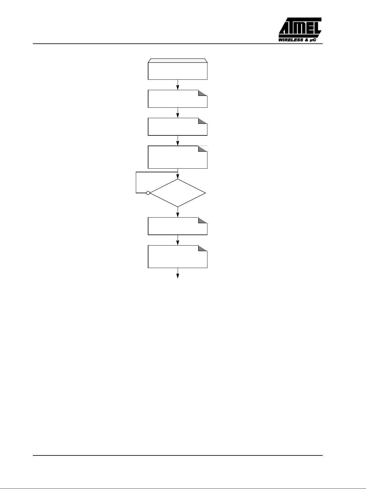
The following procedure is used to load the column latches and is summarized in Figure 8:
• Map the column latch space by setting FPS bit.
• Load the DPTR with the address to load.
• Load Accumulator register with the data to load.
• Execute the MOVX @DPTR, A instruction.
• If needed loop the three last instructions until the page is completely loaded.
Column Latches
Loading
Column Latches Mapping
Figure 8. Column Latches Loading Procedure
FPS= 1
Data Load
DPTR= Address
ACC= Data
Exec: MOVX @DPTR, A
Last Byte
to load?
Data memory Mapping
FPS= 0
22 Rev.A - May 17, 2001
Preliminary
Page 23

T89C51CC02
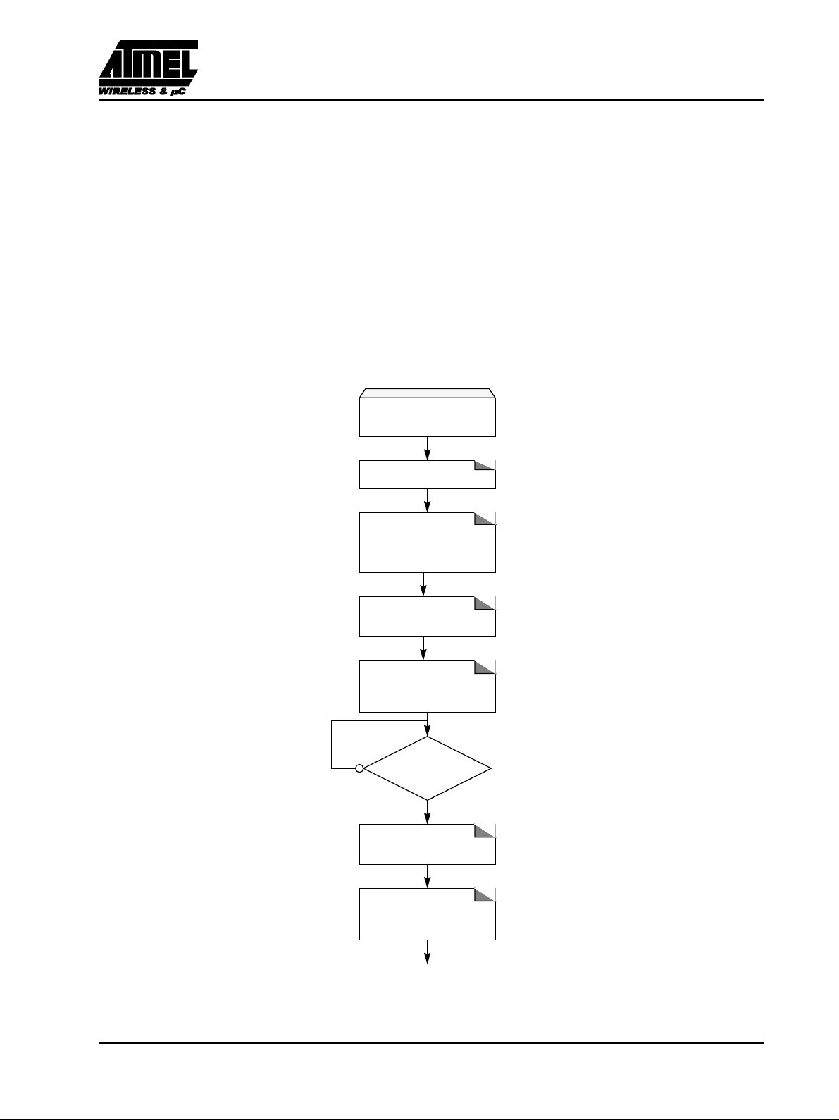
7.3.6. Programming the FLASH Spaces
User
The following procedure is used to program the User space and is summarized in Figure 9:
• Load data in the column latches from address 0000h to 3FFFh
• Disable the interrupts.
• Launch the programming by writing the data sequence 50h followed by A0h in FCON register.
The end of the programming indicated by the FBUSY flag cleared.
• Enable the interrupts.
Note:
1. The last page address used when loading the column latch is the one used to select the page programming address.
Extra Row
The following procedure is used to program the Extra Row space and is summarized in Figure 9:
• Load data in the column latches from address FF80h to FFFFh.
• Disable the interrupts.
• Launch the programming by writing the data sequence 52h followed by A2h in FCON register.
The end of the programming indicated by the FBUSY flag cleared.
• Enable the interrupts.
1
.
Rev.A - May 17, 2001 23
Preliminary
Page 24
T89C51CC02
FLASH Spaces
Programming
Column Latches Loading
see Figure 8
Disable IT
EA= 0
Launch Programming
FCON= 5xh
FCON= Axh
FBusy
Cleared?
Erase Mode
FCON = 00h
End Programming
Enable IT
EA= 1
Figure 9. Flash and Extra row Programming Procedure
24 Rev.A - May 17, 2001
Preliminary
Page 25
T89C51CC02
Hardware Security
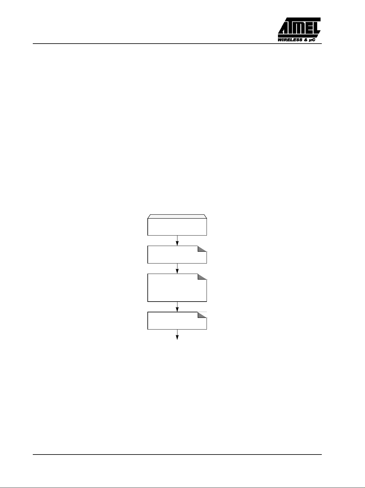
The following procedure is used to program the Hardware Security space and is summarized in Figure 10:
• Set FPS and map Harware byte (FCON = 0x0C)
• Disable the interrupts.
• Load DPTR at address 0000h.
• Load Accumulator register with the data to load.
• Execute the MOVX @DPTR, A instruction.
• Launch the programming by writing the data sequence 54h followed by A4h in FCON register.
The end of the programming indicated by the FBusy flag cleared.
• Enable the interrupts.
FLASH Spaces
Programming
FCON = 0Ch
Data Load
DPTR= 00h
ACC= Data
Exec: MOVX @DPTR, A
Disable IT
EA= 0
Launch Programming
FCON= 54h
FCON= A4h
FBusy
Cleared?
Erase Mode
FCON = 00h
End Programming
Enable IT
EA= 1
Figure 10. Hardware Programming Procedure
Rev.A - May 17, 2001 25
Preliminary
Page 26
T89C51CC02
7.3.7. Reading the FLASH Spaces
User
The following procedure is used to read the User space and is summarized in Figure 11:
• Map the User space by writing 00h in FCON register.
• Read one byte in Accumulator by executing MOVC A,@A+DPTR with A= 0 & DPTR= 0000h to FFFFh.
Extra Row
The following procedure is used to read the Extra Row space and is summarized in Figure 11:
• Map the Extra Row space by writing 02h in FCON register.
• Read one byte in Accumulator by executing MOVC A,@A+DPTR with A= 0 & DPTR= FF80h to FFFFh.
Hardware Security
The following procedure is used to read the Hardware Security space and is summarized in Figure 11:
• Map the Hardware Security space by writing 04h in FCON register.
• Read the byte in Accumulator by executing MOVC A,@A+DPTR with A= 0 & DPTR= 0000h.
FLASH Spaces
Reading
FLASH Spaces Mapping
FCON= 00000xx0b
Data Read
DPTR= Address
Exec: MOVC A, @A+DPTR
Figure 11. Reading Procedure
ACC= 0
Erase Mode
FCON = 00h
26 Rev.A - May 17, 2001
Preliminary
Page 27

T89C51CC02
7.4. Registers
FCON (S:D1h)
FLASH Control Register
7 6 5 4 3 2 1 0
FPL3 FPL2 FPL1 FPL0 FPS FMOD1 FMOD0 FBUSY
Bit Number Bit Mnemonic Description
7-4 FPL3:0
3 FPS
2-1 FMOD1:0
0 FBUSY
Reset Value= 0000 0000b
Programming Launch Command Bits
Write 5Xh followed by AXh to launch the programming according to FMOD1:0. (see Table 14.)
FLASH Map Program Space
Set to map the column latch space in the data memory space.
Clear to re-map the data memory space.
FLASH Mode
See Table 13 or Table 14.
FLASH Busy
Set by hardware when programming is in progress.
Clear by hardware when programming is done.
Can not be cleared by software.
Figure 12. FCON Register
Rev.A - May 17, 2001 27
Preliminary
Page 28

T89C51CC02
8. Data Memory
8.1. Introduction
The T89C51CC02 provides data memory access in two different spaces:
1. The internal space mapped in three separate segments:
• the lower 128 bytes RAM segment.
• the upper 128 bytes RAM segment.
• the expanded 256 bytes RAM segment (ERAM).
A fourth internal segment is available but dedicated to Special Function Registers, SFRs, (addresses 80h to FFh)
accessible by direct addressing mode.
Figure 13 shows the internal data memory spaces organization.
FFh
256 bytes
Internal ERAM
00h
FFh
80h 80h
7Fh
00h
Upper
128 bytes
Internal RAM
indirect addressing
Lower
128 bytes
Internal RAM
direct or indirect
addressing
Figure 13. Internal Data Memory Organization
FFh
Special
Function
Registers
direct addressing
28 Rev.A - May 17, 2001
Preliminary
Page 29
T89C51CC02
8.2. Internal Space
8.2.1. Lower 128 Bytes RAM
The lower 128 bytes of RAM (see Figure 13) are accessible from address 00h to 7Fh using direct or indirect
addressing modes. The lowest 32 bytes are grouped into 4 banks of 8 registers (R0 to R7). Two bits RS0 and RS1
in PSW register (see Figure 16) select which bank is in use according to Table 15. This allows more efficient use
of code space, since register instructions are shorter than instructions that use direct addressing, and can be used
for context switching in interrupt service routines.
Table 15. Register Bank Selection
RS1 RS0 Description
0 0 Register bank 0 from 00h to 07h
0 1 Register bank 0 from 08h to 0Fh
1 0 Register bank 0 from 10h to 17h
1 1 Register bank 0 from 18h to 1Fh
The next 16 bytes above the register banks form a block of bit-addressable memory space. The C51 instruction
set includes a wide selection of single-bit instructions, and the 128 bits in this area can be directly addressed by
these instructions. The bit addresses in this area are 00h to 7Fh.
7Fh
30h
20h
18h
10h
08h
00h
2Fh
Bit-Addressable Space
(Bit Addresses 0-7Fh)
1Fh
17h
4 Banks of
8 Registers
0Fh
R0-R7
07h
Figure 14. Lower 128 bytes Internal RAM Organization
8.2.2. Upper 128 Bytes RAM
The upper 128 bytes of RAM are accessible from address 80h to FFh using only indirect addressing mode.
8.2.3. Expanded RAM
The on-chip 256 bytes of expanded RAM (ERAM) are accessible from address 0000h to FFh using indirect
addressing mode through MOVX instructions.
Caution:
Lower 128 bytes RAM, Upper 128 bytes RAM, and expanded RAM are made of volatile memory cells. This means that the RAM content is
indeterminate after power-up and must then be initialized properly.
Rev.A - May 17, 2001 29
Preliminary
Page 30
T89C51CC02
8.3. Dual Data Pointer
8.3.1. Description
The T89C51CC02 implements a second data pointer for speeding up code execution and reducing code size in
case of intensive usage of external memory accesses.
DPTR0 and DPTR1 are seen by the CPU as DPTR and are accessed using the SFR addresses 83h and 84h that
are the DPH and DPL addresses. The DPS bit in AUXR1 register (see Figure 17) is used to select whether DPTR
is the data pointer 0 or the data pointer 1 (see Figure 15).
DPL0
DPL1
DPTR0
DPTR1
DPH0
DPH1
0
1
DPS
0
1
DPL
AUXR1.0
DPH
DPTR
Figure 15. Dual Data Pointer Implementation
8.3.2. Application
Software can take advantage of the additional data pointers to both increase speed and reduce code size, for
example, block operations (copy, compare, search …) are well served by using one data pointer as a “source”
pointer and the other one as a “destination” pointer.
Hereafter is an example of block move implementation using the two pointers and coded in assembler. Latest C
compiler take also advantage of this feature by providing enhanced algorithm libraries.
The INC instruction is a short (2 bytes) and fast (6 CPU clocks) way to manipulate the DPS bit in the AUXR1
register. However, note that the INC instruction does not directly force the DPS bit to a particular state, but simply
toggles it. In simple routines, such as the block move example, only the fact that DPS is toggled in the proper
sequence matters, not its actual value. In other words, the block move routine works the same whether DPS is '0'
or '1' on entry.
; ASCII block move using dual data pointers
; Modifies DPTR0, DPTR1, A and PSW
; Ends when encountering NULL character
; Note: DPS exits opposite of entry state unless an extra INC AUXR1 is added
AUXR1 EQU 0A2h
move: mov DPTR,#SOURCE ; address of SOURCE
inc AUXR1 ; switch data pointers
mov DPTR,#DEST ; address of DEST
mv_loop: inc AUXR1 ; switch data pointers
movx A,@DPTR ; get a byte from SOURCE
inc DPTR ; increment SOURCE address
inc AUXR1 ; switch data pointers
movx @DPTR,A ; write the byte to DEST
inc DPTR ; increment DEST address
jnz mv_loop ; check for NULL terminator
end_move:
30 Rev.A - May 17, 2001
Preliminary
Page 31

T89C51CC02
8.4. Registers
PSW (S:8Eh)
Program Status Word Register.
7 6 5 4 3 2 1 0
CY AC F0 RS1 RS0 OV F1 P
Bit Number Bit Mnemonic Description
7CY
6AC
5F0User Definable Flag 0.
4-3 RS1:0
2OV
1F1User Definable Flag 1.
0P
Carry Flag
Carry out from bit 1 of ALU operands.
Auxiliary Carry Flag
Carry out from bit 1 of addition operands.
Register Bank Select Bits
Refer to Table 15 for bits description.
Overflow Flag
Overflow set by arithmetic operations.
Parity Bit
Set when ACC contains an odd number of 1’s.
Cleared when ACC contains an even number of 1’s.
Reset Value= 0000 0000b
Figure 16. PSW Register
AUXR1 (S:A2h)
Auxiliary Control Register 1.
7 6 5 4 3 2 1 0
- - ENBOOT - GF3 0 - DPS
Bit Number Bit Mnemonic Description
7-6 -
5 ENBOOT
4-
3 GF3 General Purpose Flag 3.
20
1-Reserved for Data Pointer Extension.
0 DPS
Reserved
The value read from these bits is indeterminate. Do not set these bits.
Enable Boot Flash
Set this bit for map the boot flash between F800h -FFFFh
Clear this bit for disable boot flash.
Reserved
The value read from this bit is indeterminate. Do not set this bit.
Always Zero
This bit is stuck to logic 0 to allow INC AUXR1 instruction without affecting GF3 flag.
Data Pointer Select Bit
Set to select second dual data pointer: DPTR1.
Clear to select first dual data pointer: DPTR0.
Reset Value= XXXX 00X0b
Figure 17. AUXR1 Register
Rev.A - May 17, 2001 31
Preliminary
Page 32

T89C51CC02
9. EEPROM data memory
9.1. General description
The 2k byte on-chip EEPROM memory block is located at addresses 0000h to 07FFh of the ERAM memory space
and is selected by setting control bits in the EECON register.
A read in the EEPROM memory is done with a MOVX instruction.
A physical write in the EEPROM memory is done in two steps: write data in the column latches and transfer of
all data latches into an EEPROM memory row (programming).
The number of data written on the page may vary from 1 to 128 bytes (the page size). When programming, only
the data written in the column latch is programmed and a ninth bit is used to obtain this feature. This provides
the capability to program the whole memory by bytes, by page or by a number of bytes in a page. Indeed, each
ninth bit is set when the writing the corresponding byte in a row and all these ninth bits are reset after the writing
of the complete EEPROM row.
9.2. Write Data in the column latches
Data is written by byte to the column latches as for an ERAM memory. Out of the 11 address bits of the data
pointer, the 4 MSBs are used for page selection (row) and 7 are used for byte selection. Between two EEPROM
programming sessions, all the addresses in the column latches must stay on the same page, meaning that the 4
MSB must no be changed.
The following procedure is used to write to the column latches:
• Set bit EEE of EECON register
• Stretch the MOVX to accommodate the slow access time of the column latch
• Load DPTR with the address to write
• Store A register with the data to be written
• Execute a MOVX @DPTR, A
• If needed loop the three last instructions until the end of a 128 bytes page
9.3. Programming
The EEPROM programming consists on the following actions:
• writing one or more bytes of one page in the column latches. Normally, all bytes must belong to the same
page; if not, the first page address will be latched and the others discarded.
• launching programming by writing the control sequence (54h followed by A4h) to the EECON register.
• EEBUSY flag in EECON is then set by hardware to indicate that programming is in progress and that the
EEPROM segment is not available for reading.
• The end of programming is indicated by a hardware clear of the EEBUSY flag.
32 Rev.A - May 17, 2001
Preliminary
Page 33

T89C51CC02
9.4. Read Data
The following procedure is used to read the data stored in the EEPROM memory:
• Set bit EEE of EECON register
• Stretch the MOVX to accommodate the slow access time of the column latch
• Load DPTR with the address to read
• Execute a MOVX A, @DPTR
Rev.A - May 17, 2001 33
Preliminary
Page 34

T89C51CC02
9.5. Registers
EECON (S:0D2h)
EEPROM Control Register
7 6 5 4 3 2 1 0
EEPL3 EEPL2 EEPL1 EEPL0 - - EEE EEBUSY
Bit Number Bit Mnemonic Description
7-4 EEPL3-0
3-
2-
1 EEE
0 EEBUSY
Programming Launch command bits
Write 5Xh followed by AXh to EEPL to launch the programming.
Reserved
The value read from this bit is indeterminate. Do not set this bit.
Reserved
The value read from this bit is indeterminate. Do not set this bit.
Enable EEPROM Space bit
Set to map the EEPROM space during MOVX instructions (Write in the column latches)
Clear to map the ERAM space during MOVX.
Programming Busy flag
Set by hardware when programming is in progress.
Cleared by hardware when programming is done.
Can not be set or cleared by software.
Reset Value= XXXX XX00b
Not bit addressable
Figure 18. EECON Register
34 Rev.A - May 17, 2001
Preliminary
Page 35

T89C51CC02
10. In-System-Programming (ISP)
10.1. Introduction
With the implementation of the User ROM and the Boot ROM in Flash technology the T89C51CC02 allows the
system engineer the development of applications with a very high level of flexibility. This flexibility is based on
the possibility to alter the customer programming on all stages of a product’s life:
• During the final production phase, the 1st personalization of the product by parallel or serial charging of
the code in the User ROM and if wanted also a customized Boot loader in the Boot memory (Atmel will
provide also a standard Boot loader by default).
• After assembling of the product in its final, embedded position by serial mode via the CAN bus.
This In-System-Programming (ISP) allows code modification over the total lifetime of the product.
Besides the default Boot loader Atmel will provide to the customer also all the needed Application-Programming-
Interfaces (API) which are needed for the ISP. The API will be located also in the Boot memory.
This will allow the customer to have a full use of the 16 Kbyte user memory.
Two blocks flash memories are implemented (see Figure 19):
• Flash memory FM0:
containing 16 Kbytes of program memory organized in page of 128 bytes,
• Flash memory FM1:
2 Kbytes for default boot loader and Application Programming Interfaces (API).
The FM0 supports both, hardware (parallel) and software programming whereas FM1 supports only hardware
programming.
The ISP functions are assumed by:
• FCON register & bit ENBOOT in AUXR1 register,
• Software Boot Vector (SBV), which can be read and modified by using an API or the parallel programming
mode (see Figure 22)
The SBV is stored in XROW.
• The Fuse bit Boot Loader Jump Bit (BLJB) can be read and modified using an API or the parallel programming
mode.
The BLJB is located in the Hardware security byte (see Figure 24).
• The Extra Byte (EB) and Boot Status Byte (BSB) can be modified only by using API (see Figure 24).
EB is stored in XROW
The bit ENBOOT in AUXR1 register allows to map FM1 between address F800h and FFFFh of FM0.
The FM0 can be programed by:
- The Atmel boot loader, located by default in FM1.
- The user boot loader located in FM0
- The user boot loader located in FM1 in place of Atmel boot loader.
API contained in FM1 can be called by the user boot loader located in FM0 at the address [SBV]00h.
The user program simply calls the common entry point with appropriate parameters in FM1 to accomplish the
desired operation (all these methods will describe in Application Notes on api-description).
Boot Flash operations include: erase block, program byte or page, verify byte or page, program security lock bit,
etc. Indeed, Atmel provides the binary code of the default Flash boot loader.
Rev.A - May 17, 2001 35
Preliminary
Page 36

T89C51CC02
10.2. Flash Programming and Erasure
There are three methods of programming the Flash memory:
• The Atmel bootloader located in FM1 is activated by the application. Low level API routines (located in FM1)
to program FM0 will be used. The interface used for serial downloading to FM0 is the UART or the CAN.
API can be called also by user’s bootloader located in FM0 at [SBV]00h.
• A further method exist in activating the Atmel boot loader by hardware activation.
• The FM0 can be programed also by the parallel mode using a programmer.
FFFFh
2 Kbytes IAP
bootloader
F800h
3FFFh
Custom
Boot Loader
[SBV]00h
FM1
FM1 mapped between FFFF and F800
when API called
16 Kbytes
Flash memory
FM0
0000h
Figure 19. Flash Memory Mapping
36 Rev.A - May 17, 2001
Preliminary
Page 37

T89C51CC02
10.2.1. Flash Parallel Programming
The three lock bits in Hardware byte are programmed according to Table, will provide different level of protection
for the on-chip code and data located in FM0 and FM1.
The only way for write this bits are the parallel mode.
Table 16. Program Lock bit
Program Lock Bits
Security
level
1 UUU
2PUU
3 U P U Same as 2, also verify through parallel programming interface is disabled.
4 U U P Same as 3, also external execution is disabled.
Program Lock bits
LB0 LB1 LB2
No program lock features enabled. MOVC instruction executed from external program
memory returns non encrypted data.
MOVC instruction executed from external program memory are disabled from fetching
code bytes from internal memory.
Protection description
U: unprogrammed
P: programmed
WARNING: Security level 2 and 3 should only be programmed after Flash and Core verification.
Program Lock bits
These security bits protect the code access through the parallel programming interface. They are set by default to
level 4.
Rev.A - May 17, 2001 37
Preliminary
Page 38

T89C51CC02
10.3 Boot Process
10.3.1. Software boot process example
Many algorithms can be used for the software boot process. Before describing them, some explanations are needed
for the utility of different flags and bytes available.
Boot Loader Jump Bit (BLJB):
- This bit indicates if on RESET the user wants jump on his application at address @0000h on FM0 or execute
the boot loader at address @F800h on FM1.
-BLJB=0onparts delivered with bootloader programmed.
- To read or modified this bit, the APIs are used.
Boot Vector Address (SBV):
- This byte contains the msb of the user boot loader address in FM0.
- The default value of SBV is FFh (no user boot loader in FM0).
- To read or modified this byte, the APIs are used.
Extra Byte (EB) & Boot Status Byte (BSB):
- These bytes are reserved for customer use.
- To read or modified this byte, the APIs are used.
Example of software boot process in FM1 (see Figure 21)
In this example the Extra Byte (EB) is a configuration bit which forces the user boot loader execution even on
the hardware condition.
10.3.2. Hardware boot process
At the falling edge of RESET, the bit ENBOOT in AUXR1 register is initialized with the value of Boot Loader
Jump Bit (BLJB).
FCON register is initialized with the value 00h and the program in FM1 can be executed.
Check of the BLJB value.
• If bit BLJB is cleared (BLJB = 1):
User application in FM0 will be started at @0000h (standard reset).
• If bit BLJB is set (BLJB = 0):
Boot loader will be started at @F800h in FM1.
38 Rev.A - May 17, 2001
Preliminary
Page 39

T89C51CC02
Hardware
USER APPLICATION
Software
ENBOOT = 0
PC = 0000h
RESET
BLJB == 0
?
ENBOOT = 1
PC = F800h
Boot Loader
in FM1
bit ENBOOT in AUXR1 register
is initialized with BLJB.
FCON = F0h
Figure 20. Hardware Boot Process Algorithm
Rev.A - May 17, 2001 39
Preliminary
Page 40

T89C51CC02
USER APPLICATION
Hardware boot process
RESET
BLJB == 0
?
ENBOOT = 1
PC = F800h
FCON == 00h
?
bit ENBOOT in AUXR1 register
is initialized with BLJB (Fuse bit).
FCON = F0h
EB == 0
?
SBV == FFh
Software boot process
?
DEFAULT BOOT LOADERUSER BOOT LOADER
Figure 21. Example of Software Boot process
40 Rev.A - May 17, 2001
Preliminary
Page 41

T89C51CC02
10.4. 2 Application-Programming-Interface
Several Application Program Interface (API) calls are available for use by an application program to permit selective
erasing and programming of FLASH pages. All calls are made by functions.
All these APIs will be described in an application note.
API CALL Description
PROGRAM DATA BYTE Write a byte in flash memory
PROGRAM DATA PAGE Write a page (128 bytes) in flash memory
PROGRAM EEPROM BYTE Write a byte in Eeprom memory
ERASE BLOCK Erase all flash memory
ERASE BOOT VECTOR (SBV) Erase the boot vector
PROGRAM BOOT VECTOR (SBV) Write the boot vector
PROGRAM EXTRA BYTE (EB) Write the extra byte
READ DATA BYTE
READ EEPROM BYTE
READ FAMILY CODE
READ MANUFACTURER CODE
READ PRODUCT NAME
READ REVISION NUMBER
READ STATUS BIT (BSB) Read the status bit
READ BOOT VECTOR (SBV) Read the boot vector
READ EXTRA BYTE (EB) Read the extra byte
PROGRAM X2 Write the hardware flag for X2 mode
READ X2 Read the hardware flag for X2 mode
PROGRAM BLJB Write the hardware flag BLJB
READ BLJB Read the hardware flag BLJB
Rev.A - May 17, 2001 41
Preliminary
Page 42

T89C51CC02
10.5. Application remarks
After loading a new program using by the boot loader, the BLJB bit must be set to allow user application to
•
start at RESET.
• A user bootloader can be mapped at address [SBV]00h. The byte SBV contains the high byte of the boot
address, and can be read and written by API.
• The API can be called during user application, without disabling interrupt.
The interrupts are disabled by some APIs, for complex operations.
42 Rev.A - May 17, 2001
Preliminary
Page 43

T89C51CC02
10.6. XROW Bytes
Mnemonic Description Default value Address
SBV Boot Vector Address F8h 01h
SSB Software Security Byte FFh 05h
EB Extra Byte FFh 06h
Copy of the Manufacturer Code 58h 30h
Copy of the Device ID#1: Family code D7h 31h
Copy of the Device ID#2:Memories size and
type
Copy of the Device ID#3:Name and Revision FFh 61h
Table 17. Xrow mapping
SBV register
Software Boot Vector
7 6 5 4 3 2 1 0
ADD 7 ADD 6 ADD 5 ADD 4 ADD 3 ADD 2 ADD 1 ADD 0
F7h 60h
Bit Number Bit Mnemonic Description
7-0 ADD7:0 MSB of user boot loader address location
Default value after erasing chip: FFh
NOTE:
Only accessed by the API or in the parallel programming mode.
Figure 22. SBV Register
EB register
EXTRA BYTE
7 6 5 4 3 2 1 0
--------
Bit Number Bit Mnemonic Description
7-0 - User definition
Default value after erasing chip: FFh
NOTE:
TOnly accessed by the API or in the parallel programming mode.
Figure 23. EB Register
Rev.A - May 17, 2001 43
Preliminary
Page 44

T89C51CC02
10.7. Hardware Byte
7 6 5 4 3 2 1 0
X2B BLJB - - - LB2 LB1 LB0
Bit Number Bit Mnemonic Description
X2 Bit
7 X2B
6 BLJB
5-3 -
2-0 LB2:0 Lock Bits
Default value after erasing chip: FFh
NOTE:
Only the 4 MSB bits can be access by software.
The 4 LSB bits can only be access by parallel mode.
Set this bit to start in standard mode
Clear this bit to start in X2 mode.
Boot Loader Jump Bitt
Clear (=1)this bit to start the user’s application on next RESET (@0000h) located in FM0,
Set (=0)this bit to start the boot loader(@F800h) located in FM1.
Reserved
The value read from these bits are indeterminate.
Figure 24. Hardware byte
44 Rev.A - May 17, 2001
Preliminary
Page 45

T89C51CC02
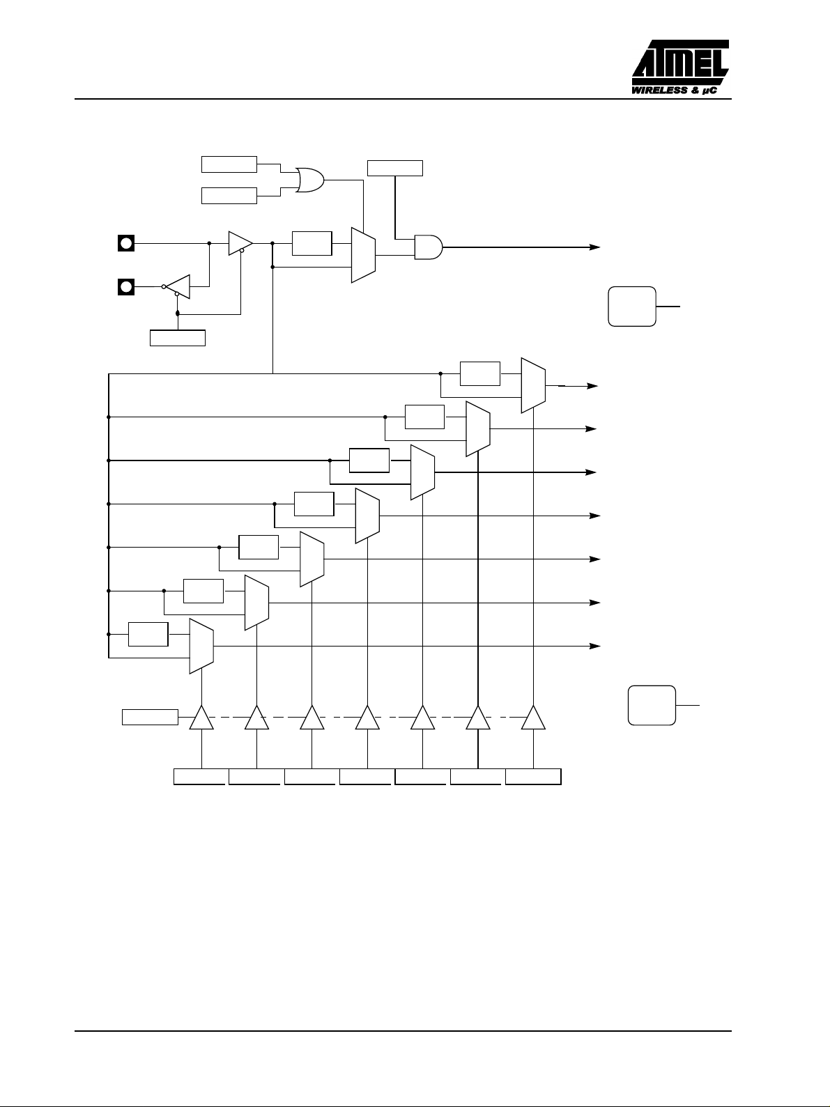
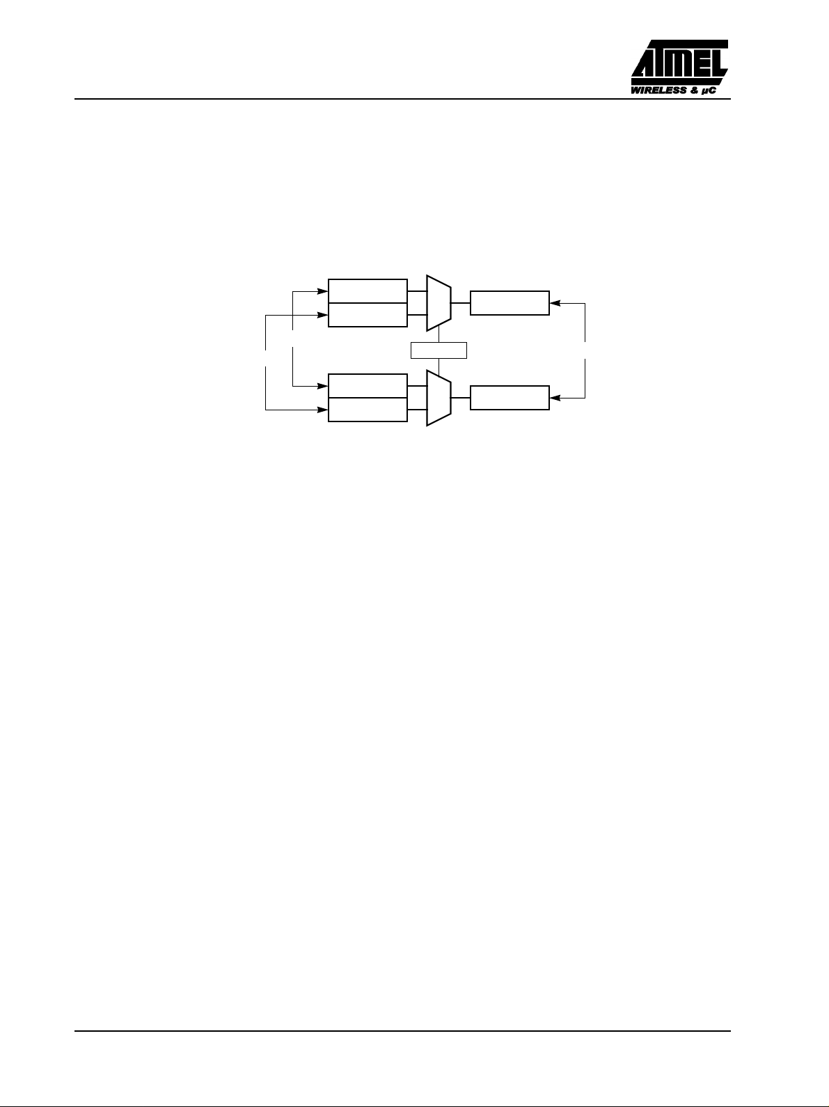
11. Serial I/O Port
The T89C51CC02 I/O serial port is compatible with the I/O serial port in the 80C52.
It provides both synchronous and asynchronous communication modes. It operates as a Universal Asynchronous
Receiver and Transmitter (UART) in three full-duplex modes (Modes 1, 2 and 3). Asynchronous transmission and
reception can occur simultaneously and at different baud rates
Serial I/O port includes the following enhancements:
• Framing error detection
• Automatic address recognition
IB Bus
TXD
RXD
Write SBUF
SBUF
Transmitter
Mode 0 Transmit
RI
TI
Figure 25. Serial I/O Port Block Diagram
SBUF
Receiver
Receive
Shift register
Read SBUF
Load SBUF
Serial Port
Interrupt Request
11.1. Framing Error Detection
Framing bit error detection is provided for the three asynchronous modes. To enable the framing bit error detection
feature, set SMOD0 bit in PCON register.
RITIRB8TB8RENSM2SM1SM0/FE
Set FE bit if stop bit is 0 (framing error)
SM0 to UART mode control
IDLPDGF0GF1POF-SMOD0SMOD1
To UART framing error control
Figure 26. Framing Error Block Diagram
When this feature is enabled, the receiver checks each incoming data frame for a valid stop bit. An invalid stop
bit may result from noise on the serial lines or from simultaneous transmission by two CPUs. If a valid stop bit
is not found, the Framing Error bit (FE) in SCON register bit is set.
Rev.A - May 17, 2001 45
Preliminary
Page 46

T89C51CC02
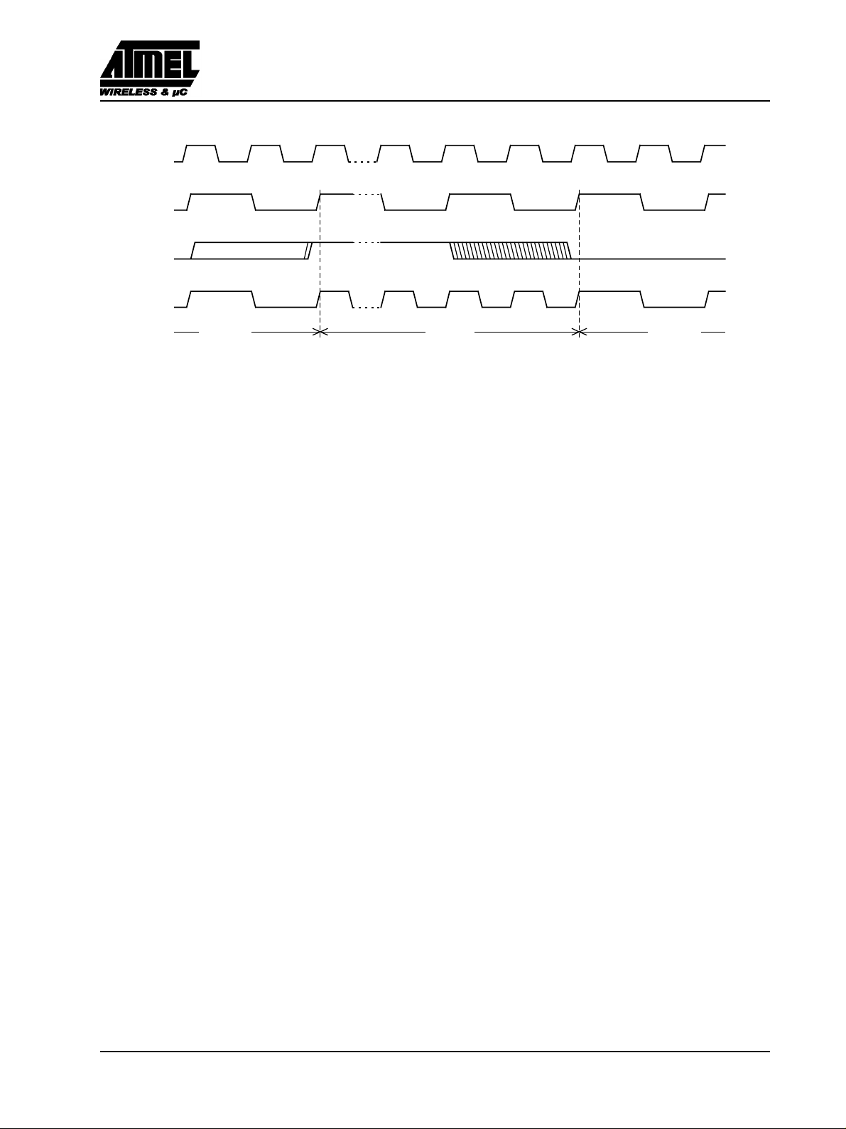
The software may examine the FE bit after each reception to check for data errors. Once set, only software or a
reset clears the FE bit. Subsequently received frames with valid stop bits cannot clear the FE bit. When the FE
feature is enabled, RI rises on the stop bit instead of the last data bit (See Figure 27. and Figure 28.).
RXD
SMOD0=X
SMOD0=1
RXD
SMOD0=0
SMOD0=1
FE
D7D6D5D4D3D2D1D0
Start
bit
RI
FE
Figure 27. UART Timing in Mode 1
Start
bit
RI
RI
Data byte
Data byte Ninth
Stop
bit
D8D7D6D5D4D3D2D1D0
bit
Stop
bit
Figure 28. UART Timing in Modes 2 and 3
11.2. Automatic Address Recognition
The automatic address recognition feature is enabled when the multiprocessor communication feature is enabled
(SM2 bit in SCON register is set).
Implemented in the hardware, automatic address recognition enhances the multiprocessor communication feature
by allowing the serial port to examine the address of each incoming command frame. Only when the serial port
recognizes its own address will the receiver set the RI bit in the SCON register to generate an interrupt. This
ensures that the CPU is not interrupted by command frames addressed to other devices.
If necessary, you can enable the automatic address recognition feature in mode 1. In this configuration, the stop
bit takes the place of the ninth data bit. Bit RI is set only when the received command frame address matches the
device’s address and is terminated by a valid stop bit.
To support automatic address recognition, a device is identified by a given address and a broadcast address.
NOTE: The multiprocessor communication and automatic address recognition features cannot be enabled in mode 0 (i.e. setting SM2 bit in SCON
register in mode 0 has no effect).
46 Rev.A - May 17, 2001
Preliminary
Page 47

T89C51CC02
11.3. Given Address
Each device has an individual address that is specified in the SADDR register; the SADEN register is a mask byte
that contains don’t-care bits (defined by zeros) to form the device’s given address. The don’t-care bits provide the
flexibility to address one or more slaves at a time. The following example illustrates how a given address is formed.
To address a device by its individual address, the SADEN mask byte must be 1111 1111b.
For example:
SADDR 0101 0110b
SADEN 1111 1100b
Given 0101 01XXb
Here is an example of how to use given addresses to address different slaves:
Slave A: SADDR 1111 0001b
SADEN 1111 1010b
Given 1111 0X0Xb
Slave B: SADDR 1111 0011b
Slave C: SADDR 1111 0010b
The SADEN byte is selected so that each slave may be addressed separately.
For slave A, bit 0 (the LSB) is a don’t-care bit; for slaves B and C, bit 0 is a 1. To communicate with slave A
only, the master must send an address where bit 0 is clear (e.g. 1111 0000b).
For slave A, bit 1 is a 0; for slaves B and C, bit 1 is a don’t care bit. To communicate with slaves A and B, but
not slave C, the master must send an address with bits 0 and 1 both set (e.g. 1111 0011b).
To communicate with slaves A, B and C, the master must send an address with bit 0 set, bit 1 clear, and bit 2
clear (e.g. 1111 0001b).
SADEN 1111 1001b
Given 1111 0XX1b
SADEN 1111 1101b
Given 1111 00X1b
11.4. Broadcast Address
A broadcast address is formed from the logical OR of the SADDR and SADEN registers with zeros defined as
don’t-care bits, e.g.:
SADDR 0101 0110b
SADEN 1111 1100b
SADDR OR SADEN 1111 111Xb
The use of don’t-care bits provides flexibility in defining the broadcast address, however in most applications, a
broadcast address is FFh. The following is an example of using broadcast addresses:
Slave A: SADDR 1111 0001b
SADEN 1111 1010b
Given 1111 1X11b,
Slave B: SADDR 1111 0011b
Slave C: SADDR= 1111 0010b
For slaves A and B, bit 2 is a don’t care bit; for slave C, bit 2 is set. To communicate with all of the slaves, the
master must send an address FFh. To communicate with slaves A and B, but not slave C, the master can send
and address FBh.
Rev.A - May 17, 2001 47
SADEN 1111 1001b
Given 1111 1X11B,
SADEN 1111 1101b
Given 1111 1111b
Preliminary
Page 48

T89C51CC02
11.5. REGISTERS
SCON (S:98h)
Serial Control Register
7 6 5 4 3 2 1 0
FE/SM0 SM1 SM2 REN TB8 RB8 TI RI
Bit Number Bit Mnemonic Description
Framing Error bit (SMOD0=1)
7FE
SM0
6 SM1
5 SM2
4 REN
3 TB8
2 RB8
1TI
0RI
Clear to reset the error state, not cleared by a valid stop bit.
Set by hardware when an invalid stop bit is detected.
Serial port Mode bit 0 (SMOD0=0)
Refer to SM1 for serial port mode selection.
Serial port Mode bit 1
SM0 SM1 ModeBaud Rate
0 0 Shift RegisterF
0 1 8-bit UARTVariable
1 0 9-bit UARTF
1 1 9-bit UARTVariable
Serial port Mode 2 bit / Multiprocessor Communication Enable bit
Clear to disable multiprocessor communication feature.
Set to enable multiprocessor communication feature in mode 2 and 3.
Reception Enable bit
Clear to disable serial reception.
Set to enable serial reception.
Transmitter Bit 8 / Ninth bit to transmit in modes 2 and 3
Clear to transmit a logic 0 in the 9th bit.
Set to transmit a logic 1 in the 9th bit.
Receiver Bit 8 / Ninth bit received in modes 2 and 3
Cleared by hardware if 9th bit received is a logic 0.
Set by hardware if 9th bit received is a logic 1.
Transmit Interrupt flag
Clear to acknowledge interrupt.
Set by hardware at the end of the 8th bit time in mode 0 or at the beginning of the stop bit in the other
modes.
Receive Interrupt flag
Clear to acknowledge interrupt.
Set by hardware at the end of the 8th bit time in mode 0, see Figure 27. and Figure 28. in the other modes.
XTAL
XTAL
/12
/64 or F
XTAL
/32
Reset Value = 0000 0000b
Bit addressable
Figure 29. SCON Register
48 Rev.A - May 17, 2001
Preliminary
Page 49

T89C51CC02
SADEN (S:B9h)
Slave Address Mask Register
7 6 5 4 3 2 1 0
Bit Number Bit Mnemonic Description
7-0 Mask Data for Slave Individual Address
Reset Value = 0000 0000b
Not bit addressable
Figure 30. SADEN Register
SADDR (S:A9h)
Slave Address Register
7 6 5 4 3 2 1 0
Bit Number Bit Mnemonic Description
7-0 Slave Individual Address
Reset Value = 0000 0000b
Not bit addressable
Figure 31. SADDR Register
SBUF (S:99h)
Serial Data Buffer
7 6 5 4 3 2 1 0
Bit Number Bit Mnemonic Description
7-0 Data sent/received by Serial I/O Port
Reset Value = 0000 0000b
Not bit addressable
Figure 32. SBUF Register
Rev.A - May 17, 2001 49
Preliminary
Page 50

T89C51CC02
PCON (S:87h)
Power Control Register
7 6 5 4 3 2 1 0
SMOD1 SMOD0 - POF GF1 GF0 PD IDL
Bit Number Bit Mnemonic Description
7 SMOD1
6 SMOD0
5-
4 POF
3 GF1
2 GF0
1PD
0 IDL
Serial port Mode bit 1
Set to select double baud rate in mode 1, 2 or 3.
Serial port Mode bit 0
Clear to select SM0 bit in SCON register.
Set to select FE bit in SCON register.
Reserved
The value read from this bit is indeterminate. Do not set this bit.
Power-Off Flag
Clear to recognize next reset type.
Set by hardware when VCC rises from 0 to its nominal voltage. Can also be set by software.
General purpose Flag
Cleared by user for general purpose usage.
Set by user for general purpose usage.
General purpose Flag
Cleared by user for general purpose usage.
Set by user for general purpose usage.
Power-Down mode bit
Cleared by hardware when reset occurs.
Set to enter power-down mode.
Idle mode bit
Clear by hardware when interrupt or reset occurs.
Set to enter idle mode.
Reset Value = 00X1 0000b
Not bit addressable
Figure 33. PCON Register
50 Rev.A - May 17, 2001
Preliminary
Page 51

T89C51CC02
12. Timers/Counters
12.1. Introduction
The T89C51CC02 implements two general-purpose, 16-bit Timers/Counters. They are identified as Timer 0 and
Timer 1, and can be independently configured to operate in a variety of modes as a Timer or as an event Counter.
When operating as a Timer, the Timer/Counter runs for a programmed length of time, then issues an interrupt
request. When operating as a Counter, the Timer/Counter counts negative transitions on an external pin. After a
preset number of counts, the Counter issues an interrupt request.
The various operating modes of each Timer/Counter are described in the following sections.
12.2. Timer/Counter Operations
For instance, a basic operation is Timer registers THx and TLx (x= 0, 1) connected in cascade to form a 16-bit
Timer. Setting the run control bit (TRx) in TCON register (see Figure 39) turns the Timer on by allowing the
selected input to increment TLx. When TLx overflows it increments THx; when THx overflows it sets the Timer
overflow flag (TFx) in TCON register. Setting the TRx does not clear the THx and TLx Timer registers. Timer
registers can be accessed to obtain the current count or to enter preset values. They can be read at any time but
TRx bit must be cleared to preset their values, otherwise the behavior of the Timer/Counter is unpredictable.
The C/Tx# control bit selects Timer operation or Counter operation by selecting the divided-down peripheral clock
or external pin Tx as the source for the counted signal. TRx bit must be cleared when changing the mode of
operation, otherwise the behavior of the Timer/Counter is unpredictable.
For Timer operation (C/Tx#= 0), the Timer register counts the divided-down peripheral clock. The Timer register
is incremented once every peripheral cycle (6 peripheral clock periods). The Timer clock rate is F
F
/ 12 in standard mode or F
OSC
For Counter operation (C/Tx#= 1), the Timer register counts the negative transitions on the Tx external input pin.
The external input is sampled every peripheral cycles. When the sample is high in one cycle and low in the next
one, the Counter is incremented. Since it takes 2 cycles (12 peripheral clock periods) to recognize a negative
transition, the maximum count rate is F
are no restrictions on the duty cycle of the external input signal, but to ensure that a given level is sampled at
least once before it changes, it should be held for at least one full peripheral cycle.
/ 6 in X2 mode.
OSC
PER
/ 12, i.e. F
/ 24 in standard mode or F
OSC
/ 12 in X2 mode. There
OSC
PER
/ 6, i.e.
12.3. Timer 0
Timer 0 functions as either a Timer or event Counter in four modes of operation. Figure 34 to Figure 37 show the
logical configuration of each mode.
Timer 0 is controlled by the four lower bits of TMOD register (see Figure 40) and bits 0, 1, 4 and 5 of TCON
register (see Figure 39). TMOD register selects the method of Timer gating (GATE0), Timer or Counter operation
(T/C0#) and mode of operation (M10 and M00). TCON register provides Timer 0 control functions: overflow flag
(TF0), run control bit (TR0), interrupt flag (IE0) and interrupt type control bit (IT0).
For normal Timer operation (GATE0= 0), setting TR0 allows TL0 to be incremented by the selected input. Setting
GATE0 and TR0 allows external pin INT0# to control Timer operation.
Timer 0 overflow (count rolls over from all 1s to all 0s) sets TF0 flag generating an interrupt request.
It is important to stop Timer/Counter before changing mode.
12.3.1. Mode 0 (13-bit Timer)
Mode 0 configures Timer 0 as an 13-bit Timer which is set up as an 8-bit Timer (TH0 register) with a modulo
32 prescaler implemented with the lower five bits of TL0 register (see Figure 34). The upper three bits of TL0
register are indeterminate and should be ignored. Prescaler overflow increments TH0 register.
Rev.A - May 17, 2001 51
Preliminary
Page 52
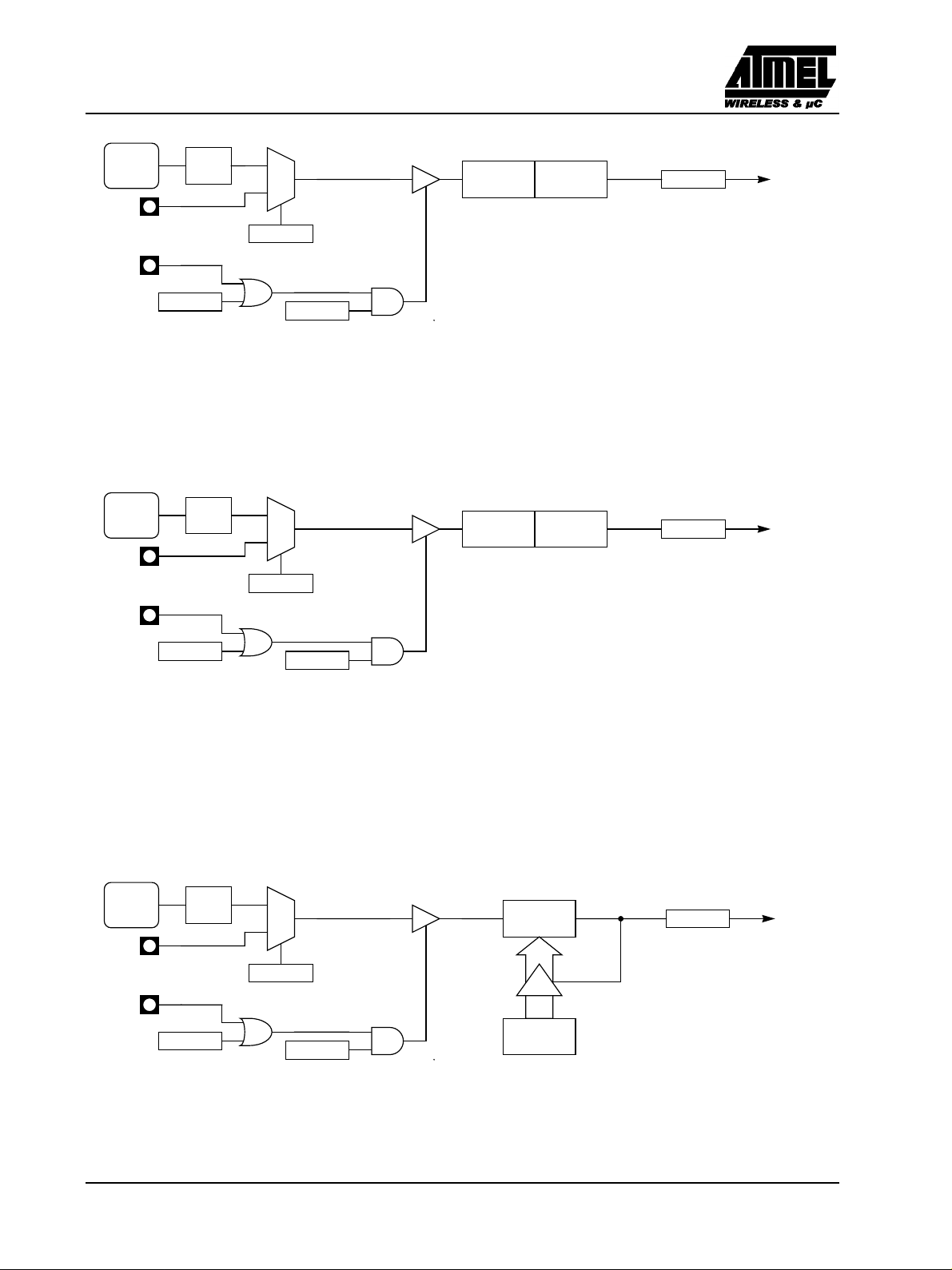
T89C51CC02
PERIPH
CLOCK
÷ 6
0
1
THx
(8 bits)
TLx
(5 bits)
Overflow
TFx
TCON reg
Timer x
Interrupt
Request
Tx
C/Tx#
TMOD reg
INTx#
GATEx
TMOD reg
TRx
TCON reg
Figure 34. Timer/Counter x (x= 0 or 1) in Mode 0
12.3.2. Mode 1 (16-bit Timer)
Mode 1 configures Timer 0 as a 16-bit Timer with TH0 and TL0 registers connected in cascade (see Figure 35).
The selected input increments TL0 register.
PERIPH
CLOCK
Tx
INTx#
÷ 6
0
1
C/Tx#
TMOD reg
THx
(8 bits)
TLx
(8 bits)
Overflow
TFx
TCON reg
Timer x
Interrupt
Request
GATEx
TMOD reg
TRx
TCON reg
Figure 35. Timer/Counter x (x= 0 or 1) in Mode 1
12.3.3. Mode 2 (8-bit Timer with Auto-Reload)
Mode 2 configures Timer 0 as an 8-bit Timer (TL0 register) that automatically reloads from TH0 register (see
Figure 36). TL0 overflow sets TF0 flag in TCON register and reloads TL0 with the contents of TH0, which is
preset by software. When the interrupt request is serviced, hardware clears TF0. The reload leaves TH0 unchanged.
The next reload value may be changed at any time by writing it to TH0 register.
PERIPH
CLOCK
Tx
INTx#
÷ 6
GATEx
TMOD reg
0
1
TLx
(8 bits)
C/Tx#
TMOD reg
THx
TRx
TCON reg
(8 bits)
Figure 36. Timer/Counter x (x= 0 or 1) in Mode 2
Overflow
TFx
TCON reg
Timer x
Interrupt
Request
52 Rev.A - May 17, 2001
Preliminary
Page 53

T89C51CC02
12.3.4. Mode 3 (Two 8-bit Timers)
Mode 3 configures Timer 0 such that registers TL0 and TH0 operate as separate 8-bit Timers (see Figure 37). This
mode is provided for applications requiring an additional 8-bit Timer or Counter. TL0 uses the Timer 0 control
bits C/T0# and GATE0 in TMOD register, and TR0 and TF0 in TCON register in the normal manner. TH0 is
locked into a Timer function (counting F
(TR1) bits. Thus, operation of Timer 1 is restricted when Timer 0 is in mode 3.
/6) and takes over use of the Timer 1 interrupt (TF1) and run control
PER
PERIPH
CLOCK
T0
INT0#
PERIPH
CLOCK
GATE0
TMOD.3
÷ 6
÷ 6
0
1
C/T0#
TMOD.2
TR0
TCON.4
TR1
TCON.6
TL0
(8 bits)
TH0
(8 bits)
Overflow
Overflow
TF0
TCON.5
TF1
TCON.7
Timer 0
Interrupt
Request
Timer 1
Interrupt
Request
Figure 37. Timer/Counter 0 in Mode 3: Two 8-bit Counters
12.4. Timer 1
Timer 1 is identical to Timer 0 excepted for Mode 3 which is a hold-count mode. Following comments help to
understand the differences:
• Timer 1 functions as either a Timer or event Counter in three modes of operation. Figure 34 to Figure 36 show
the logical configuration for modes 0, 1, and 2. Timer 1’s mode 3 is a hold-count mode.
• Timer 1 is controlled by the four high-order bits of TMOD register (see Figure 40) and bits 2, 3, 6 and 7 of
TCON register (see Figure 39). TMOD register selects the method of Timer gating (GATE1), Timer or Counter
operation (C/T1#) and mode of operation (M11 and M01). TCON register provides Timer 1 control functions:
overflow flag (TF1), run control bit (TR1), interrupt flag (IE1) and interrupt type control bit (IT1).
• Timer 1 can serve as the Baud Rate Generator for the Serial Port. Mode 2 is best suited for this purpose.
• For normal Timer operation (GATE1= 0), setting TR1 allows TL1 to be incremented by the selected input.
Setting GATE1 and TR1 allows external pin INT1# to control Timer operation.
• Timer 1 overflow (count rolls over from all 1s to all 0s) sets the TF1 flag generating an interrupt request.
• When Timer 0 is in mode 3, it uses Timer 1’s overflow flag (TF1) and run control bit (TR1). For this situation,
use Timer 1 only for applications that do not require an interrupt (such as a Baud Rate Generator for the Serial
Port) and switch Timer 1 in and out of mode 3 to turn it off and on.
• It is important to stop Timer/Counter before changing mode.
12.4.1. Mode 0 (13-bit Timer)
Mode 0 configures Timer 1 as a 13-bit Timer, which is set up as an 8-bit Timer (TH1 register) with a modulo32 prescaler implemented with the lower 5 bits of the TL1 register (see Figure 34). The upper 3 bits of TL1 register
are ignored. Prescaler overflow increments TH1 register.
Rev.A - May 17, 2001 53
Preliminary
Page 54

T89C51CC02
12.4.2. Mode 1 (16-bit Timer)
Mode 1 configures Timer 1 as a 16-bit Timer with TH1 and TL1 registers connected in cascade (see Figure 35).
The selected input increments TL1 register.
12.4.3. Mode 2 (8-bit Timer with Auto-Reload)
Mode 2 configures Timer 1 as an 8-bit Timer (TL1 register) with automatic reload from TH1 register on overflow
(see Figure 36). TL1 overflow sets TF1 flag in TCON register and reloads TL1 with the contents of TH1, which
is preset by software. The reload leaves TH1 unchanged.
12.4.4. Mode 3 (Halt)
Placing Timer 1 in mode 3 causes it to halt and hold its count. This can be used to halt Timer 1 when TR1 run
control bit is not available i.e. when Timer 0 is in mode 3.
12.5. Interrupt
Each Timer handles one interrupt source that is the timer overflow flag TF0 or TF1. This flag is set every time
an overflow occurs. Flags are cleared when vectoring to the Timer interrupt routine. Interrupts are enabled by
setting ETx bit in IEN0 register. This assumes interrupts are globally enabled by setting EA bit in IEN0 register.
TF0
TCON.5
ET0
IEN0.1
TF1
TCON.7
ET1
IEN0.3
Figure 38. Timer Interrupt System
Timer 0
Interrupt Request
Timer 1
Interrupt Request
54 Rev.A - May 17, 2001
Preliminary
Page 55

T89C51CC02
12.6. Registers
TCON (S:88h)
Timer/Counter Control Register.
7 6 5 4 3 2 1 0
TF1 TR1 TF0 TR0 IE1 IT1 IE0 IT0
Bit Number Bit Mnemonic Description
Timer 1 Overflow Flag
7 TF1
6 TR1
5 TF0
4 TR0
3 IE1
2 IT1
1 IE0
0 IT0
Cleared by hardware when processor vectors to interrupt routine.
Set by hardware on Timer/Counter overflow, when Timer 1 register overflows.
Timer 1 Run Control Bit
Clear to turn off Timer/Counter 1.
Set to turn on Timer/Counter 1.
Timer 0 Overflow Flag
Cleared by hardware when processor vectors to interrupt routine.
Set by hardware on Timer/Counter overflow, when Timer 0 register overflows.
Timer 0 Run Control Bit
Clear to turn off Timer/Counter 0.
Set to turn on Timer/Counter 0.
Interrupt 1 Edge Flag
Cleared by hardware when interrupt is processed if edge-triggered (see IT1).
Set by hardware when external interrupt is detected on INT1# pin.
Interrupt 1 Type Control Bit
Clear to select low level active (level triggered) for external interrupt 1 (INT1#).
Set to select falling edge active (edge triggered) for external interrupt 1.
Interrupt 0 Edge Flag
Cleared by hardware when interrupt is processed if edge-triggered (see IT0).
Set by hardware when external interrupt is detected on INT0# pin.
Interrupt 0 Type Control Bit
Clear to select low level active (level triggered) for external interrupt 0 (INT0#).
Set to select falling edge active (edge triggered) for external interrupt 0.
Reset Value= 0000 0000b
Figure 39. TCON Register
Rev.A - May 17, 2001 55
Preliminary
Page 56

T89C51CC02
TMOD (S:89h)
Timer/Counter Mode Control Register.
7 6 5 4 3 2 1 0
GATE1 C/T1# M11 M01 GATE0 C/T0# M10 M00
Bit Number Bit Mnemonic Description
Timer 1 Gating Control Bit
7 GATE1
6 C/T1#
5 M11
4 M01
3 GATE0
2 C/T0#
1 M10
0
M00
Clear to enable Timer 1 whenever TR1 bit is set.
Set to enable Timer 1 only while INT1# pin is high and TR1 bit is set.
Timer 1 Counter/Timer Select Bit
Clear for Timer operation: Timer 1 counts the divided-down system clock.
Set for Counter operation: Timer 1 counts negative transitions on external pin T1.
Timer 1 Mode Select Bits
M11 M01 Operating mode
0 0 Mode 0: 8-bit Timer/Counter (TH1) with 5-bit prescaler (TL1).
0 1 Mode 1: 16-bit Timer/Counter.
1 0 Mode 2: 8-bit auto-reload Timer/Counter (TL1). Reloaded from TH1 at overflow.
1 1 Mode 3: Timer 1 halted. Retains count.
Timer 0 Gating Control Bit
Clear to enable Timer 0 whenever TR0 bit is set.
Set to enable Timer/Counter 0 only while INT0# pin is high and TR0 bit is set.
Timer 0 Counter/Timer Select Bit
Clear for Timer operation: Timer 0 counts the divided-down system clock.
Set for Counter operation: Timer 0 counts negative transitions on external pin T0.
Timer 0 Mode Select Bit
M10 M00 Operating mode
0 0 Mode 0: 8-bit Timer/Counter (TH0) with 5-bit prescaler (TL0).
0 1 Mode 1: 16-bit Timer/Counter.
1 0 Mode 2: 8-bit auto-reload Timer/Counter (TL0). Reloaded from TH0 at overflow.
1 1 Mode 3: TL0 is an 8-bit Timer/Counter.
TH0 is an 8-bit Timer using Timer 1’s TR0 and TF0 bits.
Reset Value= 0000 0000b
Figure 40. TMOD Register
TH0 (S:8Ch)
Timer 0 High Byte Register.
7 6 5 4 3 2 1 0
Bit Number Bit Mnemonic Description
7:0 High Byte of Timer 0.
Reset Value= 0000 0000b
Figure 41. TH0 Register
56 Rev.A - May 17, 2001
Preliminary
Page 57

T89C51CC02
TL0 (S:8Ah)
Timer 0 Low Byte Register.
7 6 5 4 3 2 1 0
Bit Number Bit Mnemonic Description
7:0 Low Byte of Timer 0.
Reset Value= 0000 0000b
Figure 42. TL0 Register
TH1 (S:8Dh)
Timer 1 High Byte Register.
7 6 5 4 3 2 1 0
Bit Number Bit Mnemonic Description
7:0 High Byte of Timer 1.
Reset Value= 0000 0000b
Figure 43. TH1 Register
TL1 (S:8Bh)
Timer 1 Low Byte Register.
7 6 5 4 3 2 1 0
Bit Number Bit Mnemonic Description
7:0 Low Byte of Timer 1.
Reset Value= 0000 0000b
Figure 44. TL1 Register
Rev.A - May 17, 2001 57
Preliminary
Page 58

T89C51CC02
13. Timer 2
13.1. Introduction
The T89C51CC02 timer 2 is compatible with timer 2 in the 80C52.
It is a 16-bit timer/counter: the count is maintained by two eight-bit timer registers, TH2 and TL2 that are cascadeconnected. It is controlled by T2CON register (See Table 47) and T2MOD register (See Table 48). Timer 2 operation
is similar to Timer 0 and Timer 1. C/T2 selects F
as timer register input. Setting TR2 allows TL2 to be incremented by the selected input.
Timer 2 includes the following enhancements:
• Auto-reload mode (up or down counter)
• Programmable clock-output
13.2. Auto-Reload Mode
The auto-reload mode configures timer 2 as a 16-bit timer or event counter with automatic reload. This feature is
controlled by the DCEN bit in T2MOD register (See Table 48). Setting the DCEN bit enables timer 2 to count up
or down as shown in Figure 45. In this mode the T2EX pin controls the counting direction.
When T2EX is high, timer 2 up-counts. Timer overflow occurs at FFFFh which sets the TF2 flag and generates
an interrupt request. The overflow also causes the 16-bit value in RCAP2H and RCAP2L registers to be loaded
into the timer registers TH2 and TL2.
/6 (timer operation) or external pin T2 (counter operation)
OSC
When T2EX is low, timer 2 down-counts. Timer underflow occurs when the count in the timer registers TH2 and
TL2 equals the value stored in RCAP2H and RCAP2L registers. The underflow sets TF2 flag and reloads FFFFh
into the timer registers.
The EXF2 bit toggles when timer 2 overflow or underflow, depending on the direction of the count. EXF2 does
not generate an interrupt. This bit can be used to provide 17-bit resolution.
58 Rev.A - May 17, 2001
Preliminary
Page 59

T89C51CC02
T2
FT2
CLOCK
:6
0
1
CT/2
T2CON.1
(DOWN COUNTING RELOAD VALUE)
FFh
(8-bit)
TL2
(8-bit)
RCAP2L
(8-bit)
(UP COUNTING RELOAD VALUE)
FFh
(8-bit)
TH2
(8-bit)
RCAP2H
(8-bit)
TR2
T2CON.2
T2EX:
1=UP
2=DOWN
TOGGLE
TF2
T2CONreg
T2CONreg
EXF2
TIMER 2
INTERRUPT
Figure 45. Auto-Reload Mode Up/Down Counter
13.3. Programmable Clock-Output
In clock-out mode, timer 2 operates as a 50%-duty-cycle, programmable clock generator (See Figure 46). The input
clock increments TL2 at frequency F
/2. The timer repeatedly counts to overflow from a loaded value. At
OSC
overflow, the contents of RCAP2H and RCAP2L registers are loaded into TH2 and TL2. In this mode, timer 2
overflows do not generate interrupts. The formula gives the clock-out frequency depending on the system oscillator
frequency and the value in the RCAP2H and RCAP2L registers:
F
Clock OutFrequency–
NOTE: X2 bit is located in CKCON register.
In X2 mode, F
OSC=FXTAL
. In standard mode, F
OSC=FXTAL
/2.
--------------------------------------------------------------------------------------=
4 65536 RCAP2H– RCAP2L⁄()×
For a 16 MHz system clock, timer 2 has a programmable frequency range of 61 Hz (F
osc
2x2×
16)
/2
OSC
to 4 MHz (F
OSC
4). The generated clock signal is brought out to T2 pin (P1.0).
Timer 2 is programmed for the clock-out mode as follows:
• Set T2OE bit in T2MOD register.
• Clear C/T2 bit in T2CON register.
• Determine the 16-bit reload value from the formula and enter it in RCAP2H/RCAP2L registers.
/
Rev.A - May 17, 2001 59
Preliminary
Page 60

T89C51CC02
• Enter a 16-bit initial value in timer registers TH2/TL2. It can be the same as the reload value or different
depending on the application.
• To start the timer, set TR2 run control bit in T2CON register.
It is possible to use timer 2 as a baud rate generator and a clock generator simultaneously. For this configuration,
the baud rates and clock frequencies are not independent since both functions use the values in the RCAP2H and
RCAP2L registers.
FT2
CLOCK
T2EX
T2
0
1
CT/2
T2CON.1
1
0
C/T2
T2CON reg
Figure 46. Clock-Out Mode
TR2
T2CON.2
:2
EXEN2
T2CON reg
TL2
(8-bit)
RCAP2
(8-bit)
T2OE
T2MOD reg
EXF2
T2CON reg
TH2
(8-bit)
RCAP2
(8-bit)
OVERFLOW
TIMER 2
INTERRUPT
60 Rev.A - May 17, 2001
Preliminary
Page 61

T89C51CC02
13.4. Registers
T2CON (S:C8h)
Timer 2 Control Register
7 6 5 4 3 2 1 0
TF2 EXF2 RCLK TCLK EXEN2 TR2 C/T2# CP/RL2#
Bit Number Bit Mnemonic Description
Timer 2 overflow Flag
7 TF2
6 EXF2
5 RCLK
4 TCLK
3 EXEN2
2 TR2
1 C/T2#
0 CP/RL2#
TF2 is not set if RCLK=1 or TCLK = 1.
Must be cleared by software.
Set by hardware on timer 2 overflow.
Timer 2 External Flag
Set when a capture or a reload is caused by a negative transition on T2EX pin if EXEN2=1.
Set to cause the CPU to vector to timer 2 interrupt routine when timer 2 interrupt is enabled.
Must be cleared by software.
Receive Clock bit
Clear to use timer 1 overflow as receive clock for serial port in mode 1 or 3.
Set to use timer 2 overflow as receive clock for serial port in mode 1 or 3.
Transmit Clock bit
Clear to use timer 1 overflow as transmit clock for serial port in mode 1 or 3.
Set to use timer 2 overflow as transmit clock for serial port in mode 1 or 3.
Timer 2 External Enable bit
Clear to ignore events on T2EX pin for timer 2 operation.
Setto causea captureor reloadwhen anegative transitionon T2EXpin is detected, if timer 2 is not used to
clock the serial port.
Timer 2 Run control bit
Clear to turn off timer 2.
Set to turn on timer 2.
Timer/Counter 2 select bit
Clear for timer operation (input from internal clock system: F
Set for counter operation (input from T2 input pin).
Timer 2 Capture/Reload bit
If RCLK=1 or TCLK=1, CP/RL2# is ignored and timer is forced to auto-reload on timer 2 overflow.
Clear to auto-reload on timer 2 overflows or negative transitions on T2EX pin if EXEN2=1.
Set to capture on negative transitions on T2EX pin if EXEN2=1.
OSC
).
Reset Value = 0000 0000b
Bit addressable
Figure 47. T2CON Register
Rev.A - May 17, 2001 61
Preliminary
Page 62

T89C51CC02
T2MOD (S:C9h)
Timer 2 Mode Control Register
7 6 5 4 3 2 1 0
- - - - - - T2OE DCEN
Bit Number Bit Mnemonic Description
7-
6-
5-
4-
3-
2-
1 T2OE
0 DCEN
Reserved
The value read from this bit is indeterminate. Do not set this bit.
Reserved
The value read from this bit is indeterminate. Do not set this bit.
Reserved
The value read from this bit is indeterminate. Do not set this bit.
Reserved
The value read from this bit is indeterminate. Do not set this bit.
Reserved
The value read from this bit is indeterminate. Do not set this bit.
Reserved
The value read from this bit is indeterminate. Do not set this bit.
Timer 2 Output Enable bit
Clear to program P1.0/T2 as clock input or I/O port.
Set to program P1.0/T2 as clock output.
Down Counter Enable bit
Clear to disable timer 2 as up/down counter.
Set to enable timer 2 as up/down counter.
Reset Value = XXXX XX00b
Not bit addressable
Figure 48. T2MOD Register
TH2 (S:CDh)
Timer 2 High Byte Register
7 6 5 4 3 2 1 0
--------
Bit Number Bit Mnemonic Description
7-0 High Byte of Timer 2.
Reset Value = 0000 0000b
Not bit addressable
Figure 49. TH2 Register
62 Rev.A - May 17, 2001
Preliminary
Page 63

T89C51CC02
TL2 (S:CCh)
Timer 2 Low Byte Register
7 6 5 4 3 2 1 0
--------
Bit Number Bit Mnemonic Description
7-0 Low Byte of Timer 2.
Reset Value = 0000 0000b
Not bit addressable
Figure 50. TL2 Register
RCAP2H (S:CBh)
Timer 2 Reload/Capture High Byte Register
7 6 5 4 3 2 1 0
--------
Bit Number Bit Mnemonic Description
7-0 High Byte of Timer 2 Reload/Capture.
Reset Value = 0000 0000b
Not bit addressable
Figure 51. RCAP2H Register
RCAP2L (S:CAh)
Timer 2 Reload/Capture Low Byte Register
7 6 5 4 3 2 1 0
--------
Bit Number Bit Mnemonic Description
7-0 Low Byte of Timer 2 Reload/Capture.
Reset Value = 0000 0000b
Not bit addressable
Figure 52. RCAP2L Register
Rev.A - May 17, 2001 63
Preliminary
Page 64

T89C51CC02
14. WatchDog Timer
14.1. Introduction
T89C51CC02 contains a powerful programmable hardware WatchDog Timer (WDT) that automatically resets the
chip if it software fails to reset the WDT before the selected time interval has elapsed. It permits large Time-Out
ranking from 16ms to 2s @Fosc = 12MHz.
This WDT consist of a 14-bit counter plus a 7-bit programmable counter, a WatchDog Timer reset register
(WDTRST) and a WatchDog Timer programming (WDTPRG) register. When exiting reset, the WDT is -by defaultdisable. To enable the WDT, the user has to write the sequence 1EH and E1H into WDRST register. When the
WatchDog Timer is enabled, it will increment every machine cycle while the oscillator is running and there is no
way to disable the WDT except through reset (either hardware reset or WDT overflow reset). When WDT overflows,
it will generate an output RESET pulse at the RST pin. The RESET pulse duration is 96xT
F
. To make the best use of the WDT, it should be serviced in those sections of code that will periodically be
OSC
executed within the time required to prevent a WDT reset.
, where T
OSC
OSC
=1/
RESET
PERIPHERAL CLOCK
Fwd
CLOCK
WDTRST
÷PS
Enable
14-bit COUNTER
÷ 6
WR
CPU and Peripheral
Clock
Decoder
Control
7-bit COUNTER
Outputs
-
-
-
-
-
2
0
1
RESET
Figure 53. WatchDog Timer
64 Rev.A - May 17, 2001
Preliminary
Page 65

T89C51CC02
14.2. WatchDog Programming
The three lower bits (S0, S1, S2) located into WDTPRG register permits to program the WDT duration.
Table 18. Machine Cycle Count
S2 S1 S0 Machine Cycle Count
000 2
001 2
010 2
011 2
100 2
101 2
110 2
111 2
To compute WD Time-Out, the following formula is applied:
FTime Out
-------------------------------------------------------------=–
12 2
F
XTAL
142Svalue
×()1–()×
14
-1
15
-1
16
-1
17
-1
18
-1
19
-1
20
-1
21
-1
Note: Svalue represents the decimal value of (S2 S1 S0)
Find Hereafter computed Time-Out value for Fosc
Table 19. Time-Out Computation
S2 S1 S0 Fosc=12MHz Fosc=16MHz Fosc=20MHz
0 0 0 16.38 ms 12.28 ms 9.82 ms
0 0 1 32.77 ms 24.57 ms 19.66 ms
0 1 0 65.54 ms 49.14 ms 39.32 ms
0 1 1 131.07 ms 98.28 ms 78.64 ms
1 0 0 262.14 ms 196.56 ms 157.28 ms
1 0 1 524.29 ms 393.12 ms 314.56 ms
1 1 0 1.05 s 786.24 ms 629.12 ms
1 1 1 2.10 s 1.57 s 1.25 ms
XTAL
= 12MHz
Rev.A - May 17, 2001 65
Preliminary
Page 66

T89C51CC02
14.3. WatchDog Timer during Power down mode and Idle
In Power Down mode the oscillator stops, which means the WDT also stops. While in Power Down mode the
user does not need to service the WDT. There are 2 methods of exiting Power Down mode: by a hardware reset
or via a level activated external interrupt which is enabled prior to entering Power Down mode. When Power
Down is exited with hardware reset, servicing the WDT should occur as it normally does whenever T89C51CC02
is reset. Exiting Power Down with an interrupt is significantly different. The interrupt is held low long enough for
the oscillator to stabilize. When the interrupt is brought high, the interrupt is serviced. To prevent the WDT from
resetting the device while the interrupt pin is held low, the WDT is not started until the interrupt is pulled high.
It is suggested that the WDT be reset during the interrupt service for the interrupt used to exit Power Down.
To ensure that the WDT does not overflow within a few states of exiting of powerdown, it is best to reset the
WDT just before entering powerdown.
In the Idle mode, the oscillator continues to run. To prevent the WDT from resetting T89C51CC02 while in Idle
mode, the user should always set up a timer that will periodically exit Idle, service the WDT, and re-enter Idle mode.
66 Rev.A - May 17, 2001
Preliminary
Page 67

T89C51CC02
14.4. Register
WDTPRG (S:A7h)
WatchDog Timer Duration Programming register
7 6 5 4 3 2 1 0
- - - - - S2 S1 S0
Bit Number Bit Mnemonic Description
7-
6-
5-
4-
3-
2S2
1S1
0S0
Reserved
The value read from this bit is indeterminate. Do not set this bit.
Reserved
The value read from this bit is indeterminate. Do not set this bit.
Reserved
The value read from this bit is indeterminate. Do not set this bit.
Reserved
The value read from this bit is indeterminate. Do not set this bit.
Reserved
The value read from this bit is indeterminate. Do not set this bit.
WatchDog Timer Duration selection bit 2
Work in conjunction with bit 1 and bit 0.
WatchDog Timer Duration selection bit 1
Work in conjunction with bit 2 and bit 0.
WatchDog Timer Duration selection bit 0
Work in conjunction with bit 1 and bit 2.
Reset Value = XXXX X000b
Figure 54. WDTPRG Register
WDTRST (S:A6h Write only)
WatchDog Timer Enable register
7 6 5 4 3 2 1 0
--------
Bit Number Bit Mnemonic Description
7-Watchdog Control Value
Reset Value = 1111 1111b
NOTE:
The WDRST register is used to reset/enable the WDT by writing 1EH then E1H in sequence.
.
Figure 55. WDTRST Register
Rev.A - May 17, 2001 67
Preliminary
Page 68

T89C51CC02
15. Atmel CAN Controller
15.1. Introduction
The Atmel CAN Controller provides all the features required to implement the serial communication protocol CAN
as defined by the BOSCH GmbH. The CAN specifications as referred to in ISO/11898 (2.0A & 2.0B) for high
speed and ISO/11519-2 for low speed are applied. The CAN Controller is able to handle all types of frames (Data,
Remote, Error and Overload) and achieves a bitrate of 1 Mbit/s at 8MHz1Crystal frequency in X2 mode.
NOTE:
1. At BRP = 1 sampling point will be fixed.
15.2. CAN Controller Description
The CAN Controller accesses are made through SFR.
Several operations are possible by SFR:
arithmetic and logic operations, transfers and program control (SFR is accessible by direct addressing).
4 independent message objects are implemented, a pagination system manages their accesses.
Any message object can be programmed in a reception buffer block (even non-consecutive buffers). For the
reception of defined messages one or several receiver message objects can be masked without participating in the
buffer feature. An IT is generated when the buffer is full. The frames following the buffer-full interrupt will not
be taken into account until at least one of the buffer message objects is re-enabled in reception. Higher priority
of a message object for reception or transmission is given to the lower message object number.
The programmable 16-bit Timer (CANTIMER) is used to stamp each received and sent message in the CANSTMP
register. This timer starts counting as soon as the CAN controller is enabled by the ENA bit in the CANGCON register.
The Time Trigger Communication (TTC) protocol is supported by the T89C51CC02.
Bit
Stuffing /Destuffing
Cyclic
Redundancy Check
Receive Transmit
Priority
Encoder
TxDC
RxDC
Bit
Timing
Logic
Page
Register
Error
Counter
Rec/Tec
DPR(Mailbox + Registers)
µC-Core Interface
Interface
Bus
Figure 56. CAN Controller block diagram
68 Rev.A - May 17, 2001
Core
Control
Preliminary
Page 69

T89C51CC02
15.3. CAN Controller Mailbox and Registers Organization
A pagination allows management of the 48 registers and the 32 (4x8) bytes of the mailbox via 28SFR’s.
All actions on message object window SFRs are reflected to the corresponding message object registers.
SFR’s on-chip CAN Controller registers
General Control
General Status
General Interrupt
Bit Timing - 1
Bit Timing - 2
Bit Timing - 3
Enable message object
Enable Interrupt
Enable Interrupt message object
Status Interrupt message object
Timer Control
CANTimer High
CANTimer Low
TimTTC High
TimTTC Low
TEC counter
REC counter
Page message object
(message object number) (Data offset)
4 message objects
message object Status
message object Control & DLC
Message Data
ID Tag - 1
ID Tag - 2
ID Tag - 3
ID Tag - 4
ID Mask - 1
ID Mask - 2
ID Mask - 3
ID Mask - 4
TimStmp High
TimStmp Low
message object Window SFRs
message object 3 - Status
message object 0 - Status
message object 0 - Control & DLC
Ch.0 - Message Data - byte 0
8 bytes
Ch.0 - ID Tag - 1
Ch.0 - ID Tag - 2
Ch.0 - ID Tag - 3
Ch.0 - ID Tag - 4
Ch.0 - ID Mask- 1
Ch.0 - ID Mask- 2
Ch.0 - ID Mask- 3
Ch.0 - ID Mask - 4
Ch.0 TimStmp High
Ch.0 TimStmp Low
message object 3 - Control & DLC
Ch.3 - Message Data - byte 0
Ch.3 - ID Tag - 1
Ch.3 - ID Tag - 2
Ch.3 - ID Tag - 3
Ch.3 - ID Tag - 4
Ch.3 - ID Mask - 1
Ch.3 - ID Mask - 2
Ch.3 - ID Mask - 3
Ch.3 - ID Mask - 4
Ch.3 TimStmp High
Ch.3 TimStmp Low
Figure 57. CAN Controller memory organization
Rev.A - May 17, 2001 69
Preliminary
Page 70

T89C51CC02
15.3.1. Working on message objects
The Page message object register (CANPAGE) is used to select one of the 4 message objects. Then, message
object Control (CANCONCH) and message object Status (CANSTCH) are available for this selected message
object number in the corresponding SFRs. A single register (CANMSG) is used for the message. The maibox
pointer is managed by the Page message object register with an auto-incrementation at the end of each access.
The range of this counter is 8.
Note that the maibox is a pure RAM, dedicated to one message object, without overlap. In most cases, it is not
necessary to transfer the received message into the standard memory. The message to be transmitted can be built
directly in the maibox. Most calculations or tests can be executed in the mailbox area.
15.3.2. CAN Controller management
In order to enable the CAN Controller correctly the following registers have to be initialized:
• General Control (CANGCON),
• Bit Timing (CANBT 1,2&3),
• And for each page
- message object Control (CANCONCH),
- message object Status (CANSTCH).
During operation, the CAN Enable message object registers (CANEN) will give a fast overview of the message
object availability.
The CAN messages can be handled by interrupt or polling modes.
A message object can be configured as follows:
• Transmit message object,
• Receive message object,
• Receive buffer message object.
• Disable
This configuration is made in the CONCH field of the CANCONCH register (see Table 20).
When a message object is configured, the corresponding ENCH bit of CANEN register is set.
Table 20. Configuration for CONCH1:2
CONCH 1 CONCH 2 Type of message object
0 0 disable
0 1 Transmitter
1 0 Receiver
1 1 Receiver buffer
When a Transmitter or Receiver action of a message object is finished, the corresponding ENCH bit of the CANEN
register is cleared. In order to re-enable the message object, it is necessary to re-write the configuration.
Non-consecutive message objects can be used for all three types of message objects (Transmitter, Receiver and
Receiver buffer),
70 Rev.A - May 17, 2001
Preliminary
Page 71

T89C51CC02
15.3.3. Buffer mode
Any message object can be used to define the buffer, including non-consecutive message objects, and with no
limitation on length.
Each message object of the buffer must be initialized CONCH2 = 1 and CONCH1 = 1;
Block buffer
buffer 1
message object 3
message object 2
message object 1
message object 0
Figure 58. Buffer mode
buffer 0
The same acceptance filter must be defined for each message object of the buffer. When there is no mask on the
identifier or the IDE, all messages are accepted.
A received frame will always be stored in the lowest free message object.
When the flag Rxok is set on one of the buffer message objects, this message object can then be read by the
application. This flag must then be cleared by the software and the message object re-enabled in buffer reception
in order to free the message object for the next reception.
The OVRBUF flag in the CANGIT register is set when the buffer is full. This flag can generate an interrupt.
The frames following the buffer-full interrupt will not be taken into account until at least one of the buffer message
objects is re-enabled in reception.
This flag must be cleared by the software in order to acknowledge the interrupt.
Rev.A - May 17, 2001 71
Preliminary
Page 72
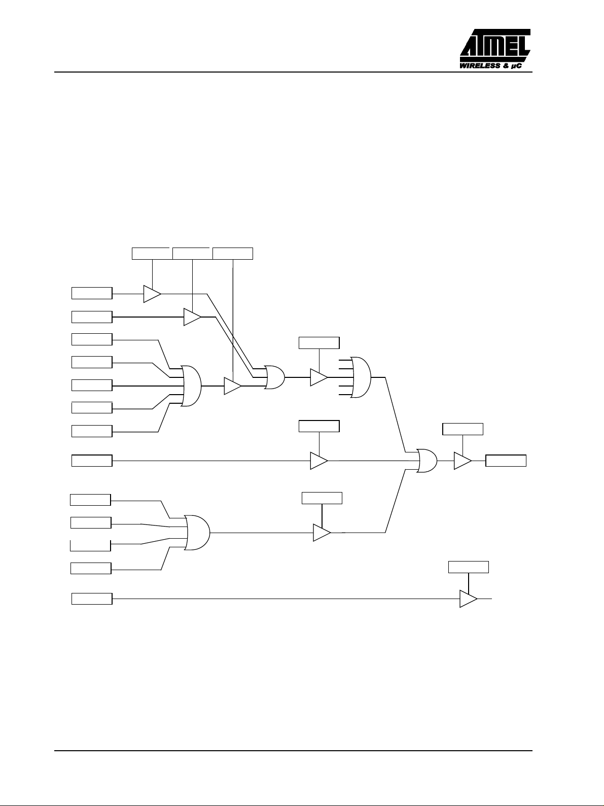
T89C51CC02
15.4. IT CAN management
The different interrupts are:
• Transmission interrupt,
• Reception interrupt,
• Interrupt on error (bit error, stuff error, crc error, form error, acknowledge error),
• Interrupt when Buffer receive is full,
• Interrupt on overrun of CAN Timer.
RXOK i
CANSTCH.5
TXOK i
CANSTCH.6
BERR i
CANSTCH.4
SERR i
CANSTCH.3
CERR i
CANSTCH.2
FERR i
CANSTCH.1
AERR i
CANSTCH.0
OVRBUF
CANGIT.4
SERG
CANGIT.3
CERG
CANGIT.2
FERG
CANGIT.1
AERG
CANGIT.0
CANGIE.5
ENRX
CANGIE.4
ENTX
CANGIE.3
ENERCH
SIT i
CANIE1/2
EICH i
CANGIE.2
ENBUF
CANGIE.1
ENERG
i=0
i=14
IEN1.0
ECAN
CANIT
CANGIT.7
IEN1.2
ETIM
OVRTIM
CANGIT.5
OVRIT
Figure 59. CAN Controller interrupt structure
72 Rev.A - May 17, 2001
Preliminary
Page 73

To enable a transmission interrupt:
• Enable General CAN IT in the interrupt system register,
• Enable interrupt by message object, EICHi,
• Enable tranmission interrupt, ENTX.
To enable a reception interrupt:
• Enable General CAN IT in the interrupt system register,
• Enable interrupt by message object, EICHi,
• Enable reception interrupt, ENRX.
To enable an interrupt on message object error:
• Enable General CAN IT in the interrupt system register,
• Enable interrupt by message object, EICHi,
• Enable interrupt on error, ENERCH.
To enable an interrupt on general error:
• Enable General CAN IT in the interrupt system register,
• Enable interrupt on error, ENERG.
To enable an interrupt on Buffer-full condition:
• Enable General CAN IT in the interrupt system register,
• Enable interrupt on Buffer full, ENBUF.
To enable an interrupt when Timer overruns:
• Enable Overrun IT in the interrupt system register.
T89C51CC02
When an interrupt occurs, the corresponding message object bit is set in the SIT register.
To acknowledge an interrupt, the corresponding CANSTCH bits (RXOK, TXOK,...) or CANGIT bits (OVRTIM,
OVRBUF,...), must be cleared by the software application.
When the CAN node is in transmission and detects a Form Error in its frame, a bit Error will also be raised.
Consequently, two consecutive interrupts can occur, both due to the same error.
When a message object error occur and set in CANSTCH register, no general error are setting in CANGIE register.
Rev.A - May 17, 2001 73
Preliminary
Page 74

T89C51CC02
15.5. Bit Timing and BaudRate
The baud rate selection is made by Tbit calculation:
Tbit = Tsyns + Tprs + Tphs1 + Tphs2
1. Tsyns = Tscl = (BRP[5..0]+ 1) / Fcan.
2. Tprs = (1 to 8) * Tscl = (PRS[2..0]+ 1) * Tscl
3. Tphs1 = (1 to 8) * Tscl = (PHS1[2..0]+ 1) * Tscl
4. Tphs2 = (1 to 8) * Tscl = (PHS2[2..0]+ 1) * Tscl
5. Tsjw = (1 to 4) * Tscl = (SJW[1..0]+ 1) * Tscl
The total number of Tscl (Time Quanta) in a bit time is from 8 to 25.
1/ Fcan
oscillator
Bit Rate Prescaler
one nominal bit
Tprs
Tphs1 + Tsjw
Tbit
Tbit Tsyns Tprs Tphs1 Tphs2++ +=
system clock
(1)
Phase error ≤ 0
(2)
Phase error ≥ 0
(3)
Phase error > 0
(4)
Phase error < 0
data
Tscl
(*)
Tsyns
(*)
Synchronization Segment: SYNS
Tsyns = 1xTscl (fixed)
Tbit calculation:
Figure 60. General structure of a bit period
example:
For a Baud Rate of 100 kbit/s and Fosc = 12 MHz For have 10 TQ:
BRP=5
PRS=2
PHS2 = 2
PHS1 = 2
Tphs1
(1)
(3)
Sample Point
(2)
Tphs2
Tphs2 - Tsjw
Transmission Point
(4)
74 Rev.A - May 17, 2001
Preliminary
Page 75

T89C51CC02
15.6. Fault Confinement
With respect to fault confinement, a unit may be in one of the three following statuses:
• error active,
• error passive,
• bus off.
An error active unit takes part in bus communication and can send an active error frame when the CAN macro
detects an error.
An error passive unit cannot send an active error frame. It takes part in bus communication, but when an error is
detected, a passive error frame is sent. Also, after a transmission, an error passive unit will wait before initiating
further transmission.
A bus off unit is not allowed to have any influence on the bus.
For fault confinement, two error counters (TEC and REC) are implemented.
See CAN Specification for details on Fault confinement.
TEC>127
or
REC>127
Error
Passive
Init.
Error
Active
TEC<127
and
REC<127
TEC>255
Figure 61. Line error mode
TEC: Transmit Error Counter
REC: Receive Error Counter
128 occurrences
of
11 consecutive
recessive
bit
Bus
Off
Rev.A - May 17, 2001 75
Preliminary
Page 76

T89C51CC02
15.7. Acceptance filter
Upon a reception hit (i.e., a good comparison between the ID+RTR+RB+IDE received and an ID+RTR+RB+IDE
specified while taking the comparison mask into account) the ID+RTR+RB+IDE received are written over the ID
TAG Registers.
RxDC
Rx Shift Register (internal)
13/32
ID TAG Registers (Ch i) & CanConch
ID RTR
Figure 62. Acceptance filter block diagram
example:
For accept only ID = 318h in part A.
ID MSK = 111 1111 1111 b
ID TAG = 011 0001 1000 b
ID RTR IDE
13/32
=
Write
Enable
13/32
IDE
13/32
1
13/32
ID MSK Registers (Ch i)
ID RTR IDE
Hit
(Ch i)
76 Rev.A - May 17, 2001
Preliminary
Page 77

15.8. Data and Remote frame
Description of the different steps for:
• Data frame,
T89C51CC02
Node A Node B
RTR
ENCH
RPLV
TXOK
message object in transmission
message object stay in
transmission
0 1 x 0 0
0 0 x 1 0
u uu uu
c uc uu
• Remote frame, with automatic reply,
RTR
ENCH
RPLV
TXOK
message object in transmission
message object in reception
by CAN controller
message object stay in
reception
1 1 x 0 0
0 1 x 1 0
0 0 x 0 1
u uu uu
c uu uc
u
c uu
c
• Remote frame.
RXOK
RXOK
REMOTE FRAME
DATA FRAME
DATA FRAME
(immediate)
RTR
ENCH
RPLV
TXOK
0 1 x 0 0
0 0 x 0 1
RTR
1 1 1 0 0
0 1 0 0 0
0 0 0 1 0
ENCH
RPLV
u uu uu
u cc uu
TXOK
u uu uu
u uu cc
c uc cu
RXOK
message object in reception
message object stay in reception
RXOK
message object in reception
message object in transmission
by CAN controller
message object stay in transmission
message object in transmission
message object in reception
by CAN controller
message object in reception
by user
RTR
ENCH
RPLV
TXOK
1 1 x 0 0
0 1 x 1 0
0 0 x 0 1
u uu uu
c uu uc
u cc uc
RXOK
REMOTE FRAME
DATA FRAME
i
: modified by user
u
(deferred)
RTR
ENCH
1 1 0 0 0
1 0 0 0 1
0 1 x 0 0
0 0 x 1 0
i
: modified by CAN
c
RPLV
TXOK
RXOK
u uu uu
u cc uu
u uu uu
c uc uu
message object in reception
message object stay in reception
message object in transmission
by user
message object stay in transmission
Rev.A - May 17, 2001 77
Preliminary
Page 78
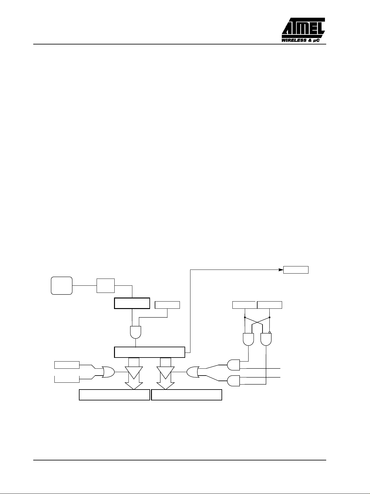
T89C51CC02
15.9. Time Trigger Communication (TTC) and Message Stamping
The T89C51CC02 has a programmable 16-bit Timer (CANTIMH&CANTIML) for message stamp and TTC.
This CAN Timer starts after the CAN controller is enabled by the ENA bit in the CANGCON register.
Two user modes of the timer are implemented:
• Time Trigger Communication:
Catch of this timer in the CANTTCH & CANTTCL registers on SOF or EOF, depending on the SYNCTTC
bit in the CANGCON register, when the network is configured in TTC by the TTC bit in the CANGCON register.
In this mode, CAN only sends the frame once, even if an error occurs.
• Message Stamping
Catch of this timer in the CANSTMPH & CANSTMPL registers of the message object which received or sent
the frame.
All messages can be stamps.
The stamping of a received frame occurs when the RxOk flag is set.
The stamping of a sent frame occurs when the TxOk flag is set.
The CAN Timer works in a loopback mode (0x0000... 0xFFFF, 0x0000) which serves as a time base to stamp all
received or transmitted messages.
When the timer overflows from 0xFFFF to 0x0000, an interrupt is generated if the ETIM bit of the CAN Timer
in a micro-controller interrupt system register is set.
Fcan
CLOCK
TXOK i
CANSTCH.4
RXOK i
CANSTCH.5
÷ 6
CANTCON
CANTIMH & CANTIML
CANSTMPH & CANSTMPL
CANGCON.1
ENA
CANTTCH & CANTTCL
When 0xFFFF to 0x0000
CANGCON.5
TTC
CANGCON.4
SYNCTTC
OVRTIM
CANGIT.5
SOF on CAN frame
EOF on CAN frame
Figure 63. Block diagram of CAN Timer
78 Rev.A - May 17, 2001
Preliminary
Page 79

T89C51CC02
15.10. CAN Autobaud and Listening mode
To activate the Autobaud feature, the AUTOBAUD bit in the CANGCON register is set. In this mode, the CAN
controller is only listening to the line without acknowledging the received messages. It cannot send any message.
The error flags are updated. The bit timing can be adjusted until no error occurs (good configuration find).
In this mode, the error counters are frozen.
To go back to the standard mode, the AUTOBAUD bit must be cleared by the software.
TxDC’
AUTOBAUD
CANGCON.3
RxDC’
TxDC
RxDC
1
0
Figure 64. Autobaud Mode
Rev.A - May 17, 2001 79
Preliminary
Page 80

T89C51CC02
15.11. CAN SFR’s
(1)
0/8
F8h
F0h
E8h
E0h
D8h
D0h
C8h
C0h
B8h
B0h
A8h
A0h
98h
90h
88h
80h
IPL1
xxxx x000CH0000 0000
B
0000 0000
IEN1
xxxx x000CL0000 0000
ACC
0000 0000
CCON
00xx xx00
PSW
0000 0000
T2CON
0000 0000
P4
xxxx xx11
IPL0
x000 0000
P3
1111 1111
IEN0
0000 0000
P2
xxx xx11
SCON
0000 0000
P1
1111 1111
TCON
0000 0000
(1)
0/8
1/9 2/A 3/B 4/C 5/D 6/E 7/F
CMOD
00xx x000
FCON
0000 0000
T2MOD
xxxx xx00
CANGIE
0000 0000
SADEN
0000 0000
CANPAGE
0000 0000
SADDR
0000 0000
CANTCON
0000 0000
SBUF
0000 0000
TMOD
0000 0000
SP
0000 0111
1/9 2/A 3/B 4/C 5/D 6/E 7/F
Table 21. CAN SFR’s with reset values
CCAP0H
0000 0000
ADCLK
xx00 x000
CCAP0L
0000 0000
CCAPM0
x000 0000
EECON
xxxx xx00
RCAP2L
0000 0000
CANSTCH
xxxx xxxx
CANGSTA
0000 0000
AUXR1
0000 0000
TL0
0000 0000
DPL
0000 0000
CCAP1H
0000 0000
ADCON
0000 0000
CCAP1L
0000 0000
CCAPM1
x000 0000
RCAP2H
0000 0000
CANIE
xxxx 0000
CANSIT
xxxx 0000
CANCONCH
xxxx xxxx
CANGCON
0000 x000
CANMSG
xxxx xxxx
CANGIT
0x00 0000
TL1
0000 0000
DPH
0000 0000
ADDL
xxxx xx00
TL2
0000 0000
CANIDM1
xxxx xxxx
CANIDT1
xxxx xxxx
CANBT1
xxxx xxxx
CANTIML
0000 0000
CANTTCL
0000 0000
CANTEC
0000 0000
TH0
0000 0000
ADDH
0000 0000
TH2
0000 0000
CANIDM2
xxxx xxxx
CANIDT2
xxxx xxxx
CANBT2
xxxx xxxx
CANTIMH
0000 0000
CANTTCH
0000 0000
CANREC
0000 0000
TH1
0000 0000
ADCF
0000 0000
CANIDM3
xxxx xxxx
CANIDT3
xxxx xxxx
CANBT3
xxxx xxxx
CANSTMPL
0000 0000
WDTRST
1111 1111
IPH1
xxxx x000
CANEN
xxxx 0000
CANIDM4
xxxx xxxx
CANIDT4
xxxx xxxx
IPH0
x000 0000
CANSTMPH
0000 0000
WDTPRG
xxxx x000
CKCON
0000 0000
PCON
0000 0000
FFh
F7h
EFh
E7h
DFh
D7h
CFh
C7h
BFh
B7h
AFh
A7h
9Fh
97h
8Fh
87h
80 Rev.A - May 17, 2001
Preliminary
Page 81

T89C51CC02
15.12. Registers
CANGCON (S:ABh)
CAN General Control Register
7 6 5 4 3 2 1 0
ABRQ OVRQ TTC SYNCTTC AUTOBAUD TEST ENA GRES
Bit Number Bit Mnemonic Description
Abort request
7 ABRQ
6 OVRQ
5 TTC
4 SYNCTTC
3 AUTOBAUD
2 TEST Test mode. The test mode is intended for factory testing and not for customer use.
1 ENA/STB
0 GRES
Not an auto-resettable bit. A reset of the ENCH bit (message object control & DLC register) is done
for each message object. The pending communications are immediately disabled and the on-going
communication will be terminated normally, setting the appropriate status flags, TXOK or RXOK.
Overload frame request (initiator).
Auto-resettable bit.
Set to send an overload frame after the next received message.
Cleared by the hardware at the beginning of transmission of the overload frame.
Network in Timer Trigger communication
0 - no TTC.
1 - node in TTC.
Synchronization of TTC
When this bit is set to "1" the TTC timer is caught on the last bit of the End Of Frame.
When this bit is set to "0" the TTC timer is caught on the Start Of Frame.
This bit is only used in the TTC mode.
AUTOBAUD
0 - no autobaud
1 - autobaud mode.
Enable/Standby CAN controller
When this bit is set to “1’, it enables the CAN controller and its input clock.
When this bit is set to “0”, the on-going communication is terminated normally and the CAN controller
state of the machine is frozen (the ENCH bit of each message object does not change).
In the standby mode, the transmitter constantly provides a recessive level; the receiver is not activated
and the input clock is stopped in the CAN controller. During the disable mode, the registers and the
mailbox remain accessible.
Note that two clock periods are needed to start the CAN controller state of the machine.
General reset (software reset).
Auto-resettable bit. This reset command is ’ORed’ with the hardware reset in order to reset the
controller. After a reset, the controller is disabled.
Reset Value: 0000 0x00b
Figure 65. CANGCON Register
Rev.A - May 17, 2001 81
Preliminary
Page 82

T89C51CC02
CANGSTA (S:AAh)
CAN General Status Register
7 6 5 4 3 2 1 0
- OVFG - TBSY RBSY ENFG BOFF ERRP
Bit Number Bit Mnemonic Description
7-
6 OVFG
5-
4 TBSY
3 RBSY
2 ENFG
1 BOFF
0 ERRP
Reserved
The values read from this bit isindeterminate. Do not set this bit.
Overload frame flag (1)
This status bit is set by the hardware as long as the produced overload frame is sent.
This flag does not generate an interrupt
Reserved
The values read from this bit isindeterminate. Do not set this bit.
Transmitter busy (1)
This status bit is set by the hardware as long as the CAN transmitter generates a frame (remote, data,
overload or error frame) or an ack field. This bit is also active during an InterFrame Spacing if a
frame must be sent.
This flag does not generate an interrupt.
Receiver busy (1)
This status bit is set by the hardware as long as the CAN receiver acquires or monitors a frame.
This flag does not generate an interrupt.
Enable on-chip CAN controller flag (1)
Because an enable/disable command is not effective immediately, this status bit gives the true state
of a chosen mode.
This flag does not generate an interrupt.
Bus off mode (1)
see Figure 61
Error passive mode (1)
see Figure 61
NOTE:
1. These fields are Read Only.
Reset Value: x0x0 0000b
Figure 66. CANGSTA Register
82 Rev.A - May 17, 2001
Preliminary
Page 83

T89C51CC02
CANGIT (S:9Bh)
CAN General Interrupt
7 6 5 4 3 2 1 0
CANIT - OVRTIM OVRBUF SERG CERG FERG AERG
Bit Number Bit Mnemonic Description
General interrupt flag (1)
7 CANIT
6-
5 OVRTIM
4 OVRBUF
3 SERG
2 CERG
1 FERG
0 AERG
This status bit is the image of all the CAN controller interrupts sent to the interrupt controller.
It can be used in the case of the polling method.
Reserved
The values read from this bit isindeterminate. Do not set this bit.
Overrun CAN Timer
This status bit is set when the CAN timer switches 0xFFFF to 0x0000.
If the ENOVRTIM bit in the IE1 register is set, an interrupt is generated.
The user clears this bit in order to reset the interrupt.
Overrun BUFFER
0 - no interrupt.
1 - IT turned on
This bit is set when the buffer is full.
Bit resettable by user.
see Figure 59.
Stuff error General
Detection of more than five consecutive bits with the same polarity.
This flag can generate an interrupt.
CRC errorGeneral
The receiver performs a CRC check on each destuffed received message from the start of frame up
to the data field.
If this checking does not match with the destuffed CRC field, a CRC error is set.
This flag can generate an interrupt.
Form error General
The form error results from one or more violations of the fixed form in the following bit fields:
CRC delimiter
acknowledgment delimiter
end_of_frame
This flag can generate an interrupt.
Acknowledgment error General
No detection of the dominant bit in the acknowledge slot.
This flag can generate an interrupt.
Reset Value: 0x00 0000b
Figure 67. CANGIT Register
Rev.A - May 17, 2001 83
Preliminary
Page 84

T89C51CC02
CANTEC (S:9Ch Read Only)
CAN Transmit Error Counter
7 6 5 4 3 2 1 0
TEC7 TEC6 TEC5 TEC4 TEC3 TEC2 TEC1 TEC0
Bit Number Bit Mnemonic Description
7-0 TEC7:0
Reset Value: 00h
CANREC (S:9Dh Read Only)
CAN Reception Error Counter
7 6 5 4 3 2 1 0
REC7 REC6 REC5 REC4 REC3 REC2 REC1 REC0
Bit Number Bit Mnemonic Description
7-0 REC7:0
Transmit Error Counter
see Figure 61
Figure 68. CANTEC Register
Reception Error Counter
see Figure 61
Reset Value: 00h
Figure 69. CANREC Register
84 Rev.A - May 17, 2001
Preliminary
Page 85

T89C51CC02
CANGIE (S:C1h)
CAN General Interrupt Enable
7 6 5 4 3 2 1 0
- - ENRX ENTX ENERCH ENBUF ENERG -
Bit Number Bit Mnemonic Description
7-6 -
5 ENRX
4 ENTX
3 ENERCH
2 ENBUF
1 ENERG
0-
Reserved
The values read from these bits are indeterminate. Do not set these bits.
Enable receive interrupt
0 - Disable
1 - Enable
Enable transmit interrupt
0 - Disable
1 - Enable
Enable message object error interrupt
0 - Disable
1 - Enable
Enable BUF interrupt
0 - Disable
1 - Enable
Enable general error interrupt
0 - Disable
1 - Enable
Reserved
The value read from this bit is indeterminate. Do not set this bit.
NOTE:
see Figure 59
Reset Value: xx00 000xb
Figure 70. CANGIE Register
CANEN (S:CFh Read Only)
CAN Enable message object Registers
7 6 5 4 3 2 1 0
- - - - ENCH3 ENCH2 ENCH1 ENCH0
Bit Number Bit Mnemonic Description
7-4 -
3-0 ENCH3:0
Reserved
The value read from these bit are indeterminate. Do not set these bits.
Enable message object
0 - message object is disabled => the message object is free for a new emission or reception.
1 - message object is enabled.
This bit is resettable by re-writing the CANCONCH of the corresponding message object.
Reset Value: xxxx 0000b
Figure 71. CANEN Register
Rev.A - May 17, 2001 85
Preliminary
Page 86

T89C51CC02
CANSIT (S:BBh Read Only)
CAN Status Interrupt message object Registers
7 6 5 4 3 2 1 0
----SIT3 SIT2 SIT1 SIT0
Bit Number Bit Mnemonic Description
7-4 -
3-0 SIT3:0
Reset Value: xxxx 0000b
CANIE (S:C3h)
CAN Enable Interrupt message object Registers
Reserved
The value read from these bit are indeterminate. Do not set these bits.
Status of interrupt by message object
0 - no interrupt.
1 - IT turned on. Reset when interrupt condition is cleared by user.
example: CANSIT = 0b 0000 1001 -> IT’s on message objects3&0.
see Figure 59.
Figure 72. CANSIT Register
7 6 5 4 3 2 1 0
----IECH 3 IECH 2 IECH 1 IECH 0
Bit Number Bit Mnemonic Description
7-4 -
3-0 IECH3:0
Reserved
The value read from these bit are indeterminate. Do not set these bits.
Enable interrupt by message object
0 - disable IT.
1 - enable IT.
example: CANIE= 0b 0000 1100 -> Enable IT’s of message objects 3 & 0.
Reset Value: xxxx 0000b
Figure 73. CANIE Register
86 Rev.A - May 17, 2001
Preliminary
Page 87

T89C51CC02
CANBT1 (S:B4h)
CAN Bit Timing Registers 1
7 6 5 4 3 2 1 0
- BRP 5 BRP 4 BRP 3 BRP 2 BRP 1 BRP 0 -
Bit Number Bit Mnemonic Description
7-
6-1 BRP5:0
Reserved
The value read from this bit is indeterminate. Do not set this bit.
Baud rate prescaler
The period of the CAN controller system clock Tscl is programmable and determines the individual
bit timing.
Tscl
BRP 5…0[]1+
-------------------------------------- -=
Fcan
0-
Note:
The CAN controller bit timing registers must be accessed only if the CAN controller is disabled with the ENA bit of the CANGCON register set to 0.
See Figure 60.
Reserved
The value read from this bit is indeterminate. Do not set this bit.
No default value after reset.
Figure 74. CANBT1 Register
Rev.A - May 17, 2001 87
Preliminary
Page 88

T89C51CC02
CANBT2 (S:B5h)
CAN Bit Timing Registers 2
7 6 5 4 3 2 1 0
- SJW 1 SJW 0 - PRS 2 PRS 1 PRS 0 -
Bit Number Bit Mnemonic Description
7-
6-5 SJW1:0
Reserved
The value read from this bit is indeterminate. Do not set this bit.
Re-synchronization jump width
To compensate for phase shifts between clock oscillators of different bus controllers, the controller
must re-synchronize on any relevant signal edge of the current transmission.
The synchronization jump width defines the maximum number of clock cycles. A bit period may be
shortened or lengthened by a re-synchronization.
Tsjw Tscl SJW 10,][ 1+()×=
4-
3-1 PRS2:0
0-
Note:
The CAN controller bit timing registers must be accessed only if the CAN controller is disabled with the ENA bit of the CANGCON register set to 0.
See Figure 60.
Reserved
The value read from this bit is indeterminate. Do not set this bit.
Programming time segment
This part of the bit time is used to compensate for the physical delay times within the network. It is
twice the sum of the signal propagation time on the bus line, the input comparator delay and the
output driver delay.
Tprs Tscl PRS 2…0][ 1+()×=
Reserved
The value read from this bit is indeterminate. Do not set this bit.
No default value after reset.
Figure 75. CANBT2 Register
88 Rev.A - May 17, 2001
Preliminary
Page 89

T89C51CC02
CANBT3 (S:B6h)
CAN Bit Timing Registers 3
7 6 5 4 3 2 1 0
- PHS2 2 PHS2 1 PHS2 0 PHS1 2 PHS1 1 PHS1 0 SMP
Bit Number Bit Mnemonic Description
7-
6-4 PHS2 2:0
3-1 PHS1 2:0
0 SMP
Reserved
The value read from this bit is indeterminate. Do not set this bit.
Phase segment 2
This phase is used to compensate for phase edge errors. This segment can be shortened by the resynchronization jump width.
Tphs2 Tscl PHS22…0][ 1+()×=
Phase segment 1
This phase is used to compensate for phase edge errors. This segment can be lengthened by the resynchronization jump width.
Tphs1 Tscl PHS12…0][ 1+()×=
Sample type
0 - once, at the sample point.
1 - three times, the threefold sampling of the bus is the sample point and twice over a distance of a
1/2 period of the Tscl. The result corresponds to the majority decision of the three values.
Note:
The CAN controller bit timing registers must be accessed only if the CAN controller is disabled with the ENA bit of the CANGCON register set to 0.
See Figure 60.
No default value after reset.
Figure 76. CANBT3 Register
CANPAGE (S:B1h)
CAN message object Page Register
7 6 5 4 3 2 1 0
- - CHNB 1 CHNB 0
Bit Number Bit Mnemonic Description
7-6 -
5-4 CHNB1:0
3 AINC
2-0 INDX2:0
Reserved
The value read from these bit are indeterminate. Do not set these bits.
Selection of message object number
The available numbers are: 0 to 3 (see Figure 57).
Auto increment of the index (active low)
0 - auto-increment of the index (default value).
1 - non-auto-increment of the index.
Index
Byte location of the data field for the defined message object (see Figure 57).
AINC INDX2 INDX1 INDX0
Reset Value: 0000 0000b
Figure 77. CANPAGE Register
Rev.A - May 17, 2001 89
Preliminary
Page 90

T89C51CC02
CANCONCH (S:B3h)
CAN message object Control and DLC Register
7 6 5 4 3 2 1 0
CONCH 1 CONCH 0 RPLV IDE DLC 3 DLC 2 DLC 1 DLC 0
Bit Number Bit Mnemonic Description
Configuration of message object
CONCH1 CONCH0
0 0: disable
7-6 CONCH1:0
5 RPLV
4 IDE
3-0 DLC3:0
0 1: Transmitter
1 0: Receiver
1 1: Receiver Buffer
NOTE:
The user must re-write the configuration to enable the corresponding bit in the CANEN1:2 registers.
Reply valid
Used in the automatic reply mode after receiving a remote frame
0 - reply not ready.
1 - reply ready & valid.
Identifier extension
0 - CAN standard rev 2.0 A (ident = 11 bits).
1 - CAN standard rev 2.0 B (ident = 29 bits).
Data length code
Number of bytes in the data field of the message.
The range of DLC is from 0 up to 8.
This value is updated when a frame is received (data or remote frame).
If the expected DLC differs from the incoming DLC, a warning appears in the CANSTCH register.
See Figure 62.
No default value after reset
Figure 78. CANCONCH Register
90 Rev.A - May 17, 2001
Preliminary
Page 91

T89C51CC02
CANSTCH (S:B2h)
CAN message object Status Register
7 6 5 4 3 2 1 0
DLCW TXOK RXOK BERR SERR CERR FERR AERR
Bit Number Bit Mnemonic Description
Data length code warning
7 DLCW
6 TXOK
5 RXOK
4 BERR
3 SERR
2 CERR
1 FERR
0 AERR
The incoming message does not have the DLC expected. Whatever the frame type, the DLC field of
the CANCONCH register is updated by the received DLC.
Transmit OK
The communication enabled by transmission is completed.
When the controller is ready to send a frame, if two or more message objects are enabled as producers,
the lower index message object (0 to 13) is supplied first.
This flag can generate an interrupt.
Receive OK
The communication enabled by reception is completed.
In the case of two or more message object reception hits, the lower index message object (0 to 13)
is updated first.
This flag can generate an interrupt.
Bit error (only in transmission)
The bit value monitored is different from the bit value sent.
Exceptions:
the monitored recessive bit sent as a dominant bit during the arbitration field and the acknowledge
slot detecting a dominant bit during the sending of an error frame.
This flag can generate an interrupt.
Stuff error
Detection of more than five consecutive bits with the same polarity.
This flag can generate an interrupt.
CRC error
The receiver performs a CRC check on each destuffed received message from the start of frame up
to the data field.
If this checking does not match with the destuffed CRC field, a CRC error is set.
This flag can generate an interrupt.
Form error
The form error results from one or more violations of the fixed form in the following bit fields:
CRC delimiter
acknowledgment delimiter
end_of_frame
This flag can generate an interrupt.
Acknowledgment error
No detection of the dominant bit in the acknowledge slot.
This flag can generate an interrupt.
NOTE:
See Figure 59.
No default value after reset.
Figure 79. CANSTCH Register
Rev.A - May 17, 2001 91
Preliminary
Page 92

T89C51CC02
CANIDT1 for V2.0 part A (S:BCh)
CAN Identifier Tag Registers 1
7 6 5 4 3 2 1 0
IDT 10 IDT 9 IDT 8 IDT 7 IDT 6 IDT 5 IDT 4 IDT 3
Bit Number Bit Mnemonic Description
7-0 IDT10:3
No default value after reset.
CANIDT2 for V2.0 part A (S:BDh)
CAN Identifier Tag Registers 2
7 6 5 4 3 2 1 0
IDT 2 IDT 1 IDT 0 - - - - -
IDentifier tag value
See Figure 62.
Figure 80. CANIDT1 Register for V2.0 part A
Bit Number Bit Mnemonic Description
7-5 IDT2:0
4-0 -
IDentifier tag value
See Figure 62.
Reserved
The values read from these bits are indeterminate. Do not set these bits.
No default value after reset.
Figure 81. CANIDT2 Register for V2.0 part A
CANIDT3 for V2.0 part A (S:BEh)
CAN Identifier Tag Registers 3
7 6 5 4 3 2 1 0
--------
Bit Number Bit Mnemonic Description
7-0 -
Reserved
The values read from these bits are indeterminate. Do not set these bits.
No default value after reset.
Figure 82. CANIDT3 Register for V2.0 part A
92 Rev.A - May 17, 2001
Preliminary
Page 93

T89C51CC02
CANIDT4 for V2.0 part A (S:BFh)
CAN Identifier Tag Registers 4
7 6 5 4 3 2 1 0
- - - - - RTRTAG - RB0TAG
Bit Number Bit Mnemonic Description
7-3 -
2 RTRTAG Remote transmission request tag value.
1-
0 RB0TAG Reserved bit 0 tag value.
No default value after reset.
CANIDT1 for V2.0 part B (S:BCh)
CAN Identifier Tag Registers 1
Reserved
The values read from these bits are indeterminate. Do not set these bits.
Reserved
The values read from this bit are indeterminate. Do not set these bit.
Figure 83. CANIDT4 Register for V2.0 part A
7 6 5 4 3 2 1 0
IDT 28 IDT 27 IDT 26 IDT 25 IDT 24 IDT 23 IDT 22 IDT 21
Bit Number Bit Mnemonic Description
7-0 IDT28:21
IDentifier tag value
See Figure 62.
No default value after reset.
Figure 84. CANIDT1 Register for V2.0 part B
CANIDT2 for V2.0 part B (S:BDh)
CAN Identifier Tag Registers 2
7 6 5 4 3 2 1 0
IDT 20 IDT 19 IDT 18 IDT 17 IDT 16 IDT 15 IDT 14 IDT 13
Bit Number Bit Mnemonic Description
7-0 IDT20:13
IDentifier tag value
See Figure 62.
No default value after reset.
Figure 85. CANIDT2 Register for V2.0 part B
Rev.A - May 17, 2001 93
Preliminary
Page 94

T89C51CC02
CANIDT3 for V2.0 part B (S:BEh)
CAN Identifier Tag Registers 3
7 6 5 4 3 2 1 0
IDT 12 IDT 11 IDT 10 IDT 9 IDT 8 IDT 7 IDT 6 IDT 5
Bit Number Bit Mnemonic Description
7-0 IDT12:5
No default value after reset.
CANIDT4 for V2.0 part B (S:BFh)
CAN Identifier Tag Registers 4
7 6 5 4 3 2 1 0
IDT 4 IDT 3 IDT 2 IDT 1 IDT 0 RTRTAG RB1TAG RB0TAG
IDentifier tag value
See Figure 62.
Figure 86. CANIDT3 Register for V2.0 part B
Bit Number Bit Mnemonic Description
7-3 IDT4:0
2 RTRTAG Remote transmission request tag value
1 RB1TAG Reserved bit 1 tag value.
0 RB0TAG Reserved bit 0 tag value.
IDentifier tag value
See Figure 62.
No default value after reset.
Figure 87. CANIDT4 Register for V2.0 part B
CANIDM1 for V2.0 part A (S:C4h)
CAN Identifier Mask Registers 1
7 6 5 4 3 2 1 0
IDMSK 10 IDMSK 9 IDMSK 8 IDMSK 7 IDMSK 6 IDMSK 5 IDMSK 4 IDMSK 3
Bit Number Bit Mnemonic Description
IDentifier mask value
7-0 IDTMSK10:3
0 - comparison true forced.
1 - bit comparison enabled.
See Figure 62.
No default value after reset.
Figure 88. CANIDM1 Register for V2.0 part A
94 Rev.A - May 17, 2001
Preliminary
Page 95

T89C51CC02
CANIDM2 for V2.0 part A (S:C5h)
CAN Identifier Mask Registers 2
7 6 5 4 3 2 1 0
IDMSK 2 IDMSK 1 IDMSK 0 -----
Bit Number Bit Mnemonic Description
IDentifier mask value
7-5 IDTMSK2:0
4-0 -
No default value after reset.
CANIDM3 for V2.0 part A (S:C6h)
CAN Identifier Mask Registers 3
0 - comparison true forced.
1 - bit comparison enabled.
See Figure 62.
Reserved
The values read from these bits are indeterminate. Do not set these bits.
Figure 89. CANIDM2 Register for V2.0 part A
7 6 5 4 3 2 1 0
--------
Bit Number Bit Mnemonic Description
7-0 -
Reserved
The values read from these bits are indeterminate.
No default value after reset.
Figure 90. CANIDM3 Register for V2.0 part A
Rev.A - May 17, 2001 95
Preliminary
Page 96

T89C51CC02
CANIDM4 for V2.0 part A (S:C7h)
CAN Identifier Mask Registers 4
7 6 5 4 3 2 1 0
-----RTRMSK - IDEMSK
Bit Number Bit Mnemonic Description
7-3 -
2 RTRMSK
1-
0 IDEMSK
NOTE:
The ID Mask is only used for reception.
No default value after reset.
Reserved
The values read from these bits are indeterminate. Do not set these bits.
Remote transmission request mask value
0 - comparison true forced.
1 - bit comparison enabled.
Reserved
The value read from this bit is indeterminate. Do not set this bit.
IDentifier Extension mask value
0 - comparison true forced.
1 - bit comparison enabled.
Figure 91. CANIDM4 Register for V2.0 part A
CANIDM1 for V2.0 part B (S:C4h)
CAN Identifier Mask Registers 1
7 6 5 4 3 2 1 0
IDMSK 28 IDMSK 27 IDMSK 26 IDMSK 25 IDMSK 24 IDMSK 23 IDMSK 22 IDMSK 21
Bit Number Bit Mnemonic Description
IDentifier mask value
7-0 IDMSK28:21
NOTE:
The ID Mask is only used for reception.
0 - comparison true forced.
1 - bit comparison enabled.
See Figure 62.
No default value after reset.
Figure 92. CANIDM1 Register for V2.0 part B
96 Rev.A - May 17, 2001
Preliminary
Page 97

T89C51CC02
CANIDM2 for V2.0 part B (S:C5h)
CAN Identifier Mask Registers 2
7 6 5 4 3 2 1 0
IDMSK 20 IDMSK 19 IDMSK 18 IDMSK 17 IDMSK 16 IDMSK 15 IDMSK 14 IDMSK 13
Bit Number Bit Mnemonic Description
IDentifier mask value
7-0 IDMSK20:13
NOTE:
The ID Mask is only used for reception.
No default value after reset.
CANIDM3 for V2.0 part B (S:C6h)
CAN Identifier Mask Registers 3
0 - comparison true forced.
1 - bit comparison enabled.
See Figure 62.
Figure 93. CANIDM2 Register for V2.0 part B
7 6 5 4 3 2 1 0
IDMSK 12 IDMSK 11 IDMSK 10 IDMSK 9 IDMSK 8 IDMSK 7 IDMSK 6 IDMSK 5
Bit Number Bit Mnemonic Description
IDentifier mask value
7-0 IDMSK12:5
NOTE:
The ID Mask is only used for reception.
0 - comparison true forced.
1 - bit comparison enabled.
See Figure 62.
No default value after reset.
Figure 94. CANIDM3 Register for V2.0 part B
Rev.A - May 17, 2001 97
Preliminary
Page 98

T89C51CC02
CANIDM4 for V2.0 part B (S:C7h)
CAN Identifier Mask Registers 4
7 6 5 4 3 2 1 0
IDMSK 4 IDMSK 3 IDMSK 2 IDMSK 1 IDMSK 0 RTRMSK - IDEMSK
Bit Number Bit Mnemonic Description
IDentifier mask value
7-3 IDMSK4:0
2 RTRMSK
1-
0 IDEMSK
NOTE:
The ID Mask is only used for reception.
No default value after reset.
0 - comparison true forced.
1 - bit comparison enabled.
See Figure 62.
Remote transmission request mask value
0 - comparison true forced.
1 - bit comparison enabled.
Reserved
The value read from this bit is indeterminate. Do not set this bit.
IDentifier Extension mask value
0 - comparison true forced.
1 - bit comparison enabled.
Figure 95. CANIDM4 Register for V2.0 part B
CANMSG (S:A3h)
CAN Message Data Register
7 6 5 4 3 2 1 0
MSG 7 MSG 6 MSG 5 MSG 4 MSG 3 MSG 2 MSG 1 MSG 0
Bit Number Bit Mnemonic Description
Message data
This register contains the mailbox data byte pointed at the page message object register.
7-0 MSG7:0
After writing in the page message object register, this byte is equal to the specified message location
(in the mailbox) of the pre-defined identifier + index. If auto-incrementation is used, at the end of
the data register writing or reading cycle, the mailbox pointer is auto-incremented. The dynamic of
the counting is 8 with no end loop (0, 1,..., 7, 0,...)
No default value after reset.
Figure 96. CANMSG Register
98 Rev.A - May 17, 2001
Preliminary
Page 99

T89C51CC02
CANTCON (S:A1h)
CAN Timer ClockControl
7 6 5 4 3 2 1 0
TPRESC 7 TPRESC 6 TPRESC 5 TPRESC 4 TPRESC 3 TPRESC 2 TPRESC 1 TPRESC 0
Bit Number Bit Mnemonic Description
Timer Prescaler of CAN Timer
7-0 TPRESC7:0
Reset Value: 00h
CANTIMH (S:ADh Read Only)
CAN Timer High
7 6 5 4 3 2 1 0
CANGTIM 15 CANGTIM 14 CANGTIM 13 CANGTIM 12 CANGTIM 11 CANGTIM 10 CANGTIM 9 CANGTIM 8
This register is a prescaler for the main timer upper counter
range=0to255.
See Figure 63.
Figure 97. CANTCON Register
Bit Number Bit Mnemonic Description
7-0 CANGTIM15:8
High byte of Message Timer
See Figure 63.
Reset Value: 0000 0000b
Figure 98. CANTIMH Register
CANTIML (S:ACh Read Only)
CAN Timer Low
7 6 5 4 3 2 1 0
CANGTIM 7 CANGTIM 6 CANGTIM 5 CANGTIM 4 CANGTIM 3 CANGTIM 2 CANGTIM 1 CANGTIM 0
Bit Number Bit Mnemonic Description
7-0 CANGTIM7:0
Low byte of Message Timer
See Figure 63.
Reset Value: 0000 0000b
Figure 99. CANTIML Register
Rev.A - May 17, 2001 99
Preliminary
Page 100

T89C51CC02
CANSTMPH (S:AFh Read Only)
CAN Stamp Timer High
7 6 5 4 3 2 1 0
TIMSTMP 15 TIMSTMP 14 TIMSTMP 13 TIMSTMP 12 TIMSTMP 11 TIMSTMP 10 TIMSTMP 9 TIMSTMP 8
Bit Number Bit Mnemonic Description
7-0 TIMSTMP15:8
No default value after reset
CANSTMPL (S:AEh Read Only)
CAN Stamp Timer Low
7 6 5 4 3 2 1 0
TIMSTMP 7 TIMSTMP 6 TIMSTMP 5 TIMSTMP 4 TIMSTMP 3 TIMSTMP 2 TIMSTMP 1 TIMSTMP 0
High byte of Time Stamp
See Figure 63.
Figure 100. CANSTMPH Register
Bit Number Bit Mnemonic Description
7-0 TIMSTMP7:0
Low byte of Time Stamp
See Figure 63.
No default value after reset
Figure 101. CANSTMPL Register
CANTTCH (S:A5h Read Only)
CAN TTC Timer High
7 6 5 4 3 2 1 0
TIMTTC 15 TIMTTC 14 TIMTTC 13 TIMTTC 12 TIMTTC 11 TIMTTC 10 TIMTTC 9 TIMTTC 8
Bit Number Bit Mnemonic Description
7-0 TIMTTC15:8
High byte of TTC Timer
See Figure 63.
Reset Value: 0000 0000b
Figure 102. CANTTCH Register
100 Rev.A - May 17, 2001
Preliminary
 Loading...