

Page 1

1. Features
• 80C51 core architecture:
– 256 bytes of on-chip RAM
– 1 Kbytes of on-chip ERAM
– 32 Kbytes of on-chip Flash memory
Data Retention: 10 years at 85°C
Read/Write cycle: 10k
– 2 Kbytes of on-chip Flash for Bootloader
– 2 Kbytes of on-chip EEPROM
Read/Write cycle: 100k
– 14-sources 4-level interrupts
– Three 16-bit timers/counters
– Full duplex UART compatible 80C51
– Maximum crystal frequency 40 MHz. In X2 mode, 20 MHz (CPU core, 40 MHz)
– Five ports: 32 + 2 digital I/O lines
– Five-channel 16-bit PCA with:
PWM (8-bit)
High-speed output
Timer and edge capture
– Double Data Pointer
– 21-bit watchdog timer (7 programmable bits)
• A 10-bit r esolution analog to digitalconverter (ADC) with 8 m ultiplexed inputs
• Full CAN controller:
– Fully compliant with CAN rev2.0A and 2.0B
– Optimized structure for communication management (via SFR)
– 15 independent message objects:
Each message object programmable on transmission or reception
individual tag and mask filters up to 29-bit identifier/channel
8-byte cyclic data register (FIFO)/message object
16-bit status & control register/message object
16-bit Time-Stamping register/message object
CAN specification 2.0 part A or 2.0 part B programmable for each message
object
Access to message object control and data registers via SFR
Programmable reception buffer length up to 15 message objects
Priority management of reception of hits on several message objects at the
same time (Basic CAN Feature)
Priority management for transmission
message object overrun interrupt
– Supports
Time Triggered Communication
Autobaud and Listening mode
Programmable Automatic reply mode
– 1 Mbit/s maximum transfer rate at 8MHz* Crystal frequency in X2 mode.
– Readable error counters
– Programmable link to on-chip Timer for Time Stamping and Net work
synchronization
– Independent baud rate prescaler
– Data, Remote, Error and overload frame handling
• On-chip emulation Logic (enhanced Hook system)
• Power saving modes:
– Idle mode
– Power down mode
• Power supply: 5V +/- 10% (or 3V** +/- 10%)
• Temperature range: Industrial (-40° to +85°C)
• Packages: VQFP44, PLCC44, CA-BGA64
Note:
* AtB RP = 1 samplingpoint will be fixed.
** Askfor availability
Enhance d 8-bit
MCU with CAN
controller and
Flash
T89C51CC01
Rev. D – 17-Dec-01
1
Page 2
2. Description The T89C51CC01 is the first member of t he C A Nary
dedicated to CAN network applications.
In X2 mode a maximum external clock rate of 20 MHz reaches a 300 ns cycle time.
Besides the full CAN controller T89C51CC 01 provides 32 Kbytes of Flash memory
including I n-System Programming (ISP), 2Kbytes Boot Flash Mem ory, 2 Kbytes
EEPROM a nd 1.2 Kbyte RAM.
Primary attention is paid to the reduction of the electro-magnetic emission of
T89C51CC01.
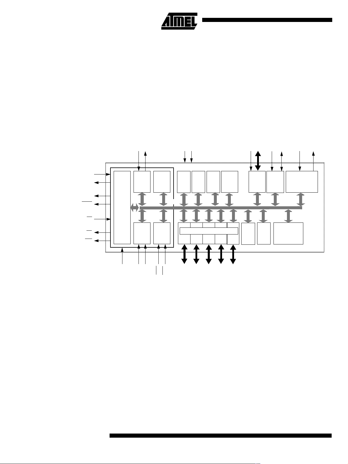
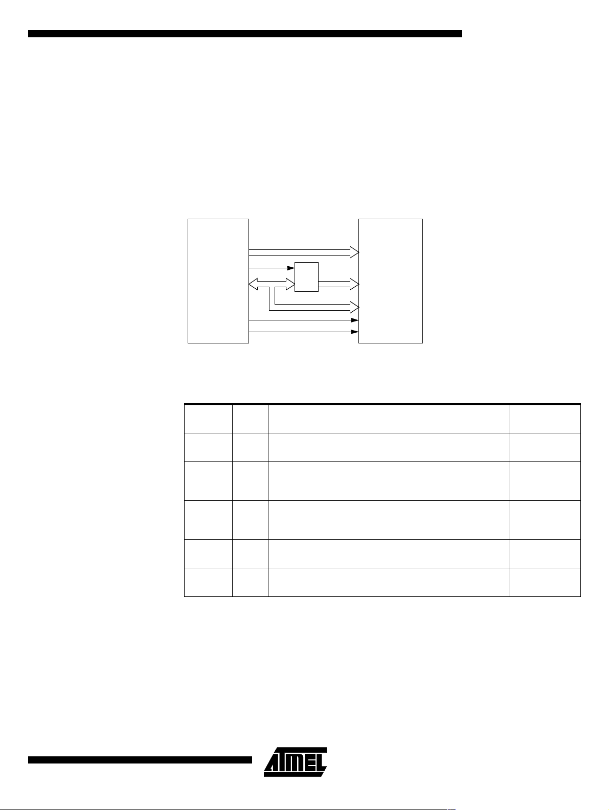
3. Block Diagram
RxD
TxD
Vss
Vcc
TM
family of 8-bit microcont rollers
PCA
ECI
T2EX
T2
RxDC
TxDC
XTAL1
XTAL2
ALE
PSEN
EA
RD
WR
CPU
T0
C51
CORE
T1
RAM
256x8
INT
Ctrl
INT0
UART
Timer 0
Timer 1
RESET
Flash
Boot
32kx
loader
8
2kx8
IB-bus
Parallel I/O Ports & Ext. Bus
Port 0P0Port 1
INT1
(1): 8 analog Inputs / 8 Digital I/O
(2): 2-BitI/O Port
Port 2
P1(1)
EE
PROM
2kx8
P2
Port 3
ERAM
1kx8
Port 4
P3
PCA
Timer2
Emul
Watch
P4(2)
Dog
Unit
CAN
CONTROLLER
10 bit
ADC
2
T89C51CC01
Rev. D – 17-Dec-01
Page 3
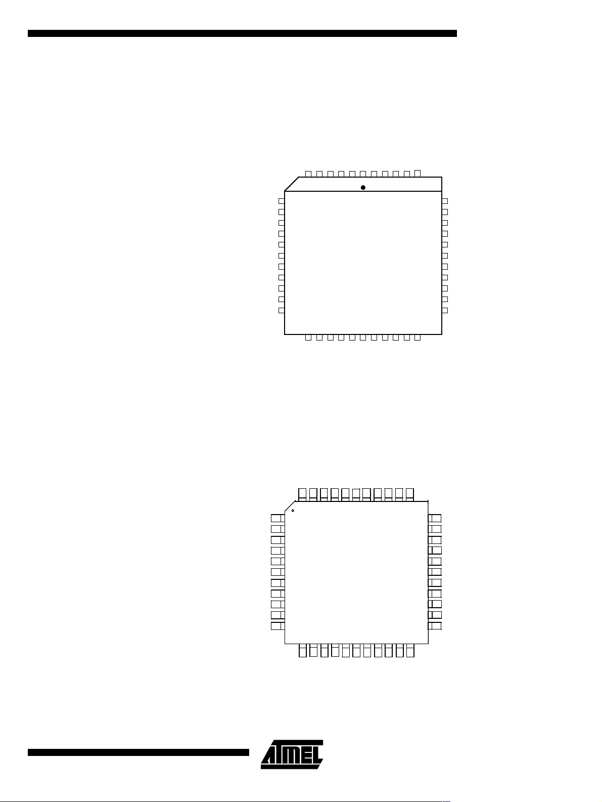
4. Pin Configuration
P1.4 / AN4 / CEX1
P1.5 / AN5 / CEX2
P1.6 / AN6 / CEX3
P1.7 / AN7 / CEX4
EA
P3.0/ RxD
P3.1 / TxD
P3.2 / INT0
P3.3 / INT1
P3.4 / T0
P3.5 / T1
7
8
9
10
11
12
13
14
15
16
17
P1.3 / AN3 / CEX0
P1.2 / A N2 / ECI
P1.1 / AN1 / T2EX
P1.0 / AN 0 / T2
65432
PLCC44
VAREF
VAGND
RESET
1
4443424140
T89C51CC01
VSS
VCC
XTAL1
XTAL2
39
ALE
38
PSEN
37
P0.7 / AD7
36
P0.6 / AD6
35
P0.5 / AD5
34
P0.4 / AD4
33
P0.3 / AD3
32
P0.2 / AD2
31
P0.1 / AD1
30
P0.0 / AD0
29
P2.0 / A8
P1.4 / AN4 / CEX1
P1.5 / AN5 / CEX2
P1.6 / AN6 / CEX3
P1.7 / AN7 / CEX4
EA
P3.0 / RxD
P3.1 / TxD
P3.2 / INT0
P3.3 / INT1
P3.4/ T0
P3.5/ T1
1819202122232425262728
P3.7/ RD
P3.6 / WR
P1.3 / AN3 / CEX0
P1.2 / AN2 / ECI
43 42 41 40 3944
1
2
3
4
5
6
7
8
9
10
11
P4.0/ TxDC
P4.1 / RxDC
P1.1 / AN1 / T2EX
P1.0/ AN0 /T2
VQFP44
P2.7/ A15
P2.6/ A14
P2.5/ A13
VAREF
VAGND
RESET
38 37 36 35 34
VSS
12 13 17161514 201918 21 22
P2.4/ A12
P2.1 / A9
P2.3/ A11
P2.2/ A10
VCC
XTAL1
XTAL2
33
ALE
32
PSEN
31
P0.7 / AD7
30
P0.6 / AD6
29
P0.5 / AD5
28
P0.4 /AD4
27
P0.3 /AD3
26
P0.2 /AD2
25
P0.1 /AD1
24
P0.0 /AD0
23
P2.0 / A8
Rev. D – 17-Dec-01
P3.7 / RD
P3.6 / WR
P2.7 / A15
P2.6 / A14
P2.5 / A13
P4.0 / TxDC
P4.1 / RxDC
P2.4 / A12
P2.1 / A9
P2.3 / A11
P2.2 / A10
3
Page 4
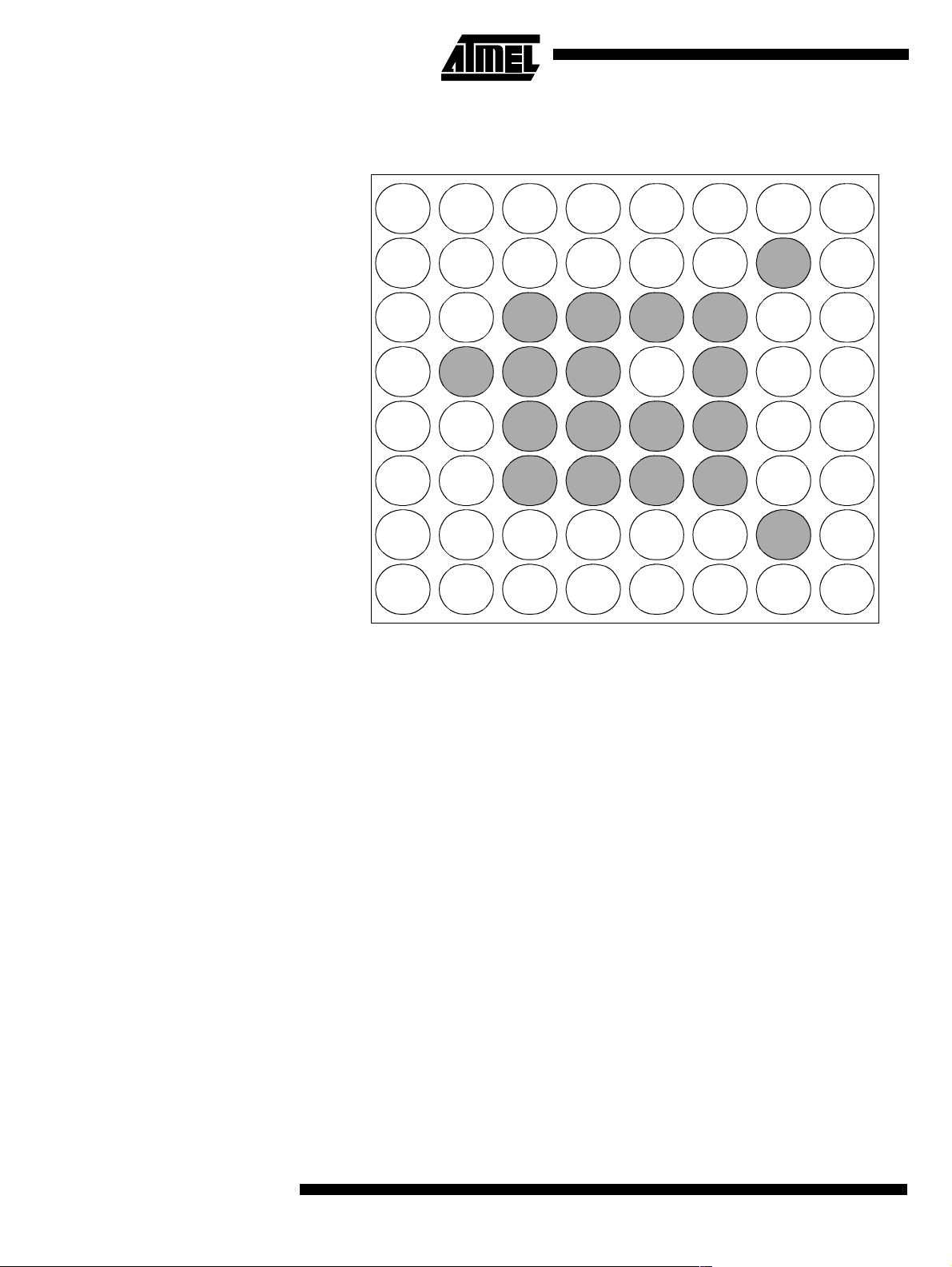
21 345678
A
B
C
D
E
F
G
H
EA
P3.0
P3.2
P3.4
P3.6
P1.2/AN2P1.4/AN4 P1.0/AN0
P1.3/AN3P1.5/AN5
P1.6/AN6
NC
P3.1
P3.3 NC
P3.5
P1.1/AN1
NC
NC NC RESET
NC
P4.0
P2.7P3.7
VAGND
VAREF VDD
NCP1.7/AN7
NC
NC
P4.1
P2.6
VSS
VDD
NC
NC
NC
P2.4
P2.5 P2.3 P2.1 P2.0
VSS XTAL1
NC P0.6
NC P0.2 P0.4
NC P0.1 P0.3
P2.2 NC P0.0
CA-BGA64 Top View
NC ALE
PSENNC
XTAL2
P0.7
P0.5
4
T89C51CC01
Rev. D – 17-Dec-01
Page 5

Table 1. Pin Description
Pin Name Type Description
VSS GND Circuit ground.
VCC Supply Voltage.
VAREF Reference Voltage for ADC
VAGND Reference Groundf or ADC
Port 0:
Is an 8-bit opendrain bi-directional I/O port.Port 0 pins that have 1’swritten to them float, and in thisstate canbe usedas
P0.0:7 I/O
P1.0:7 I/O
high-impedanceinputs. Port 0 is alsothemultiplexed low-order address and databusduring accesses to external Program
and Data Memory. In this application it uses strong internal pull-ups when emitting 1’s.
Port0 also outputs thecodebytes duringprogram validation. Externalpull-upsarerequiredduring program verification.
Port 1:
Is an 8-bit bi-directional I/Oport with internal pull-ups. Port1 pins can be usedfordigitalinput/outputor as analog inputsfor
the Analog Digital Converter (ADC). Port 1 pins that have 1’s written to them are pulled high by the internal pull-up transistors
and can be used as inputs in this state. As inputs, Port 1 pins that are being pulled low externally will be the source of current
(I
, see section "Electrical Characteristic")because of the internal pull-ups.Port1pinsare assignedtobeusedasanalog
IL
inputsvia the ADCCF register (in thiscasethe internal pull-ups are disconnected).
As a secondary digital function, port 1 contains the Timer 2 external trigger and clock input; the PCA external clock input and
the PCA module I/O.
P1.0 / AN0 / T2
Analoginput channel 0,
External clock input for Timer/counter2.
P1.1 / AN1 / T2EX
Analoginput channel 1,
Trigger inputfor Timer/counter2.
P1.2 / AN2 / ECI
Analoginput channel 2,
PCA externalclock input.
P1.3 / AN3 / CEX0
Analoginput channel 3,
PCA module 0 Entry of input/PWM output.
P1.4 / AN4 / CEX1
Analoginput channel 4,
PCA module 1 Entry of input/PWM output.
P1.5 / AN5 / CEX2
Analoginput channel 5,
PCA module 2 Entry of input/PWM output.
P1.6 / AN6 / CEX3
Analoginput channel 6,
PCA module 3 Entry of input/PWM output.
P1.7 / AN7 / CEX4
Analoginput channel 7,
PCA module 4 Entry ot input/PWM output.
Port1 receives the low-order address byte during EPROM programmingandprogramverification.
It can driveCMOSinputs withoutexternalpull-ups.
T89C51CC01
P2.0:7 I/O
Rev. D – 17-Dec-01
Port 2:
Is an 8-bit bi-directional I/Oport with internal pull-ups.Port2 pinsthathave 1’s written to them arepulled highby theinternal
pull-ups and can be used as inputs in this state. As inputs, Port 2 pins that are being pulled low externally will be a source of
current (I
duringaccesses to the external Program Memory and during accessestoexternal Data Memory thatuses 16-bitaddresses
(MOVX @DPTR). In thisapplication, it uses strong internal pull-ups when emitting 1’s.During accesses to external Data
Memory thatuse 8 bit addresses (MOVX @Ri), Port 2 transmits the contents of the P2 special functionregister.
It also receives high-orderaddressesandcontrol signalsduringprogram validation.
It can driveCMOSinputs withoutexternalpull-ups.
, see section "Electrical Characteristic") because of the internal pull-ups. Port 2 emitsthehigh-order address byte
IL
5
Page 6

Pin Name Type Description
Port 3:
Is an 8-bit bi-directional I/Oport with internal pull-ups.Port3 pinsthathave 1’s written to them arepulled highby theinternal
pull-up transistors and can be used as inputs in this state. As inputs, Port 3 pins that are being pulled low externally will be a
P3.0:7 I/O
P4.0:1 I/O
sourceofcurrent (I
The output latch corresponding to a secondary function must be programmed to one for that function to operate (except for
TxD and WR
P3.0 / RxD:
Receiver datainput (asynchronous)or data input/output(synchronous) of the serial interface
P3.1 / TxD:
Transmitter data output(asynchronous)orclock output(synchronous) of the serial interface
P3.2 / INT0
External interrupt 0 input/ timer0 gate control input
P3.3 / INT1
External interrupt 1 input/ timer1 gate control input
P3.4 / T0:
Timer0counterinput
P3.5 / T1:
Timer1counterinput
P3.6 / WR
External Data Memory write strobe; latches the data byte from port 0 into the external data memory
P3.7 / RD
External Data Memory read strobe; Enables the external data memory.
It can driveCMOSinputs withoutexternalpull-ups.
Port 4:
Is an 2-bit bi-directional I/Oport with internal pull-ups.Port4 pinsthathave 1’s written to them arepulled highby theinternal
pull-ups and can be used as inputs in this state. As inputs, Port 4 pins that are being pulled low externally will be a source of
current (IIL, on the datasheet) because of the internalpull-up transistor.
The output latch corresponding to a secondary function RxDC must be programmed to one for that function to operate. The
secondary functions are assigned to the two pins of port4as follows:
P4.0 / TxDC:
Transmitter output of CAN controller
P4.1 / RxDC:
Receiver input of CAN controller.
It can driveCMOSinputs withoutexternalpull-ups.
:
:
:
:
, see section"Electrical Characteristic")because of the internal pull-ups.
IL
). The secondary functions are assigned to the pins of port 3 as follows:
6
T89C51CC01
Rev. D – 17-Dec-01
Page 7

Pin Name Type Description
Reset:
RESET I/O
ALE O
PSEN O
EA I
XTAL1 I
A high level on this pin during two machine cycles while the oscillator is running resets the device. An internal pull-down
resistor to VSS permits power-on reset using only an external capacitor to VCC.
ALE:
An Address Latch Enableoutput for latching the low byte of the addressduringaccesses to theexternalmemory. The ALEis
activated every1/6oscillator periods(1/3 in X2 mode) exceptduring an external datamemory access.When instructionsare
executed from an internal FLASH(EA
PSEN
:
The Program Store Enable output is a control signal that enables the external program memory of the bus during external
fetch operations. It is activatedtwice each machine cycleduring fetches from the external program memory. However, when
executingfromofthe externalprogrammemory twoactivations ofPSENare skippedduring each access to the externalData
memory.ThePSENisnot activatedfor internalfetches.
EA
:
When ExternalAccess isheld at thehigh level, instructionsare fetchedfrom theinternalFLASH whenthe programcounter is
less then 8000H. When held at the low level,T89C51CC01 fetches all instructions from the external program memory
XTAL1:
Input of the inverting oscillator amplifier and input of the internal clock generator circuits.
To drivethedevicefromanexternalclock source, XTAL1 shouldbedriven,whileXTAL2 isleft unconnected. To operate
abovea frequency of 16 MHz, a duty cycleof50%should be maintained.
= 1), ALE generationcanbedisabledby thesoftware.
T89C51CC01
.
XTAL2 O
XTAL2:
Outputfrom the inverting oscillator amplifier.
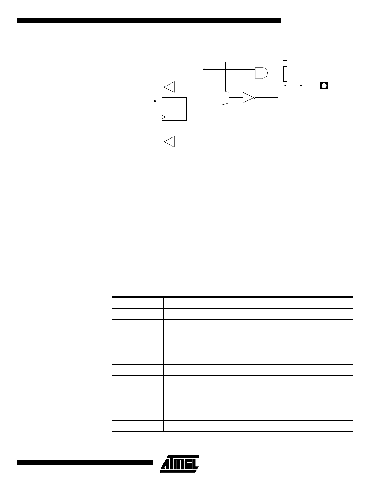
4.2 I/O Configurations Each Port SFR operates via type-D latches, as illustrated in Figure 1 for Ports 3 and 4. A
CPU "wri te to la tch" signal initiates t rans f er of internal bus data into the type-D latch. A
CPU "read latch" signal tr ans f ers the latched Q output onto the internal bus. Similarly, a
"read pin" signal transfe rs the logical level of the Port pin. Some P ort data instructions
activate the "read latch" signal while others activate the " re ad pin" signal. Latch instructions are re ferre d to as Read-M odif y-Writ e in structi ons. Each I/O line may b e
independently programm ed as input or output.
4.3 Port 1, Port 3 and Port 4
Figure 1 shows the structure of Ports 1 and 3, which have internal pull-ups. An external
source can pull the pin low. Each Port pin can be configured either for general purpose
I/O or for its alternate input output func tion.
To use a pin for general purpose output, set or clear the corresponding bit in the Px register (x=1,3 or 4). To use a pin for general purpose input, set the bit in the Px regist er.
This turns off the output FET drive.
To configure a pi n for its alternate function, set the bit in the Px regist er. When the latch
is set, the "alternate output function" signal controls the output level (see Figure 1). The
operation of Port s 1, 3 and 4 is discussed further in "quasi-Bidirectional Port Operation"
paragraph.
Rev. D – 17-Dec-01
7
Page 8
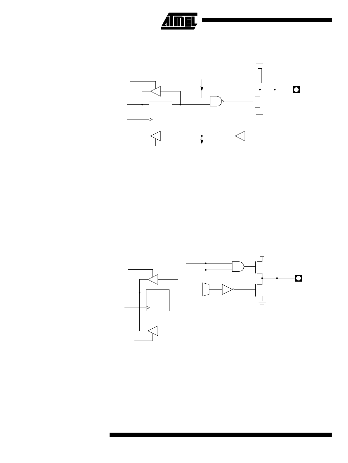
Figure 1. Port 1, Port 3 and Port 4 Structure
VCC
READ
LATCH
ALTERNATE
OUTPUT
FUNCTION
INTERNAL
PULL-UP (1)
P1.x
P3.x
INTERNAL
BUS
WRITE
TO
LATCH
READ
PIN
D
CL
P3.X
P4.X
LATCH
QP1.X
ALTERNATE
INPUT
FUNCTION
P4.x
Note: The internal pull-up can be disabled on P1 when analog function is selected.
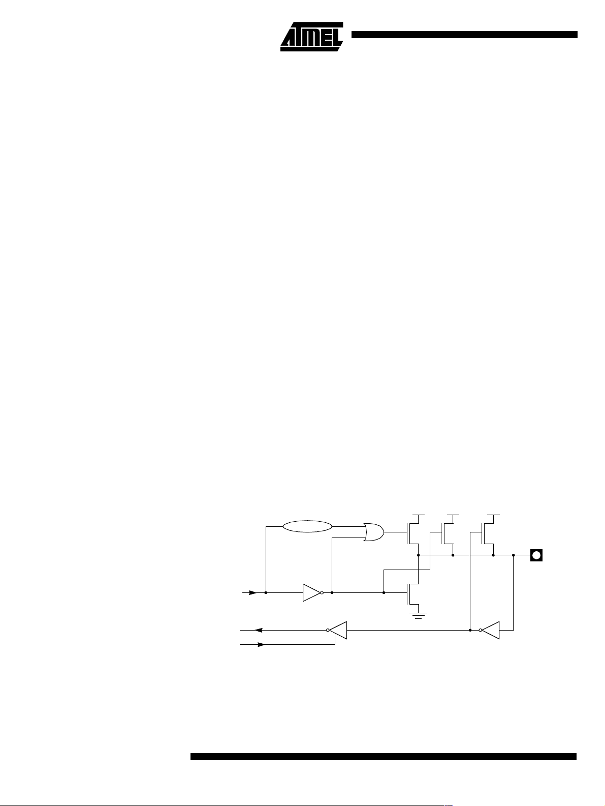
4.4 Port 0 and Port2 Ports 0 and 2 are used for general-purpose I/O or as the external address /data bus. Port
0, shown in Figure 3, differs from t he other Ports in not having internal pull-ups. Figure 3
shows the structure of Port 2. An external source can pul l a Port 2 pin low.
To use a pin for general-purpose output, set or c lear the corresponding bit in t he Px register ( x =0 or 2). To us e a pin for general purpose input, set the bit in the Px regist er to
turn off the output driver FET.
Figure 2. Port 0 Structure
READ
LATCH
INTERNAL
BUS
WRITE
TO
LATCH
READ
PIN
D
P0.X
LATCH
ADDRESS LOW/
DATA
Q
CONTROL
1
0
VDD
(2)
P0.x (1)
Notes: 1. Port 0 is precluded from use as general purpose I/O Ports when used as
address/data bus drivers.
2. Port 0 internalstrong pull-upsassist the logic-one output for memory bus cycles only.
Except for these bus cycles, the pull-up FET is off, Port 0 outputs are open-drain.
8
T89C51CC01
Rev. D – 17-Dec-01
Page 9
T89C51CC01
Figure 3. Port 2 Structure
READ
LATCH
INTERNAL
BUS
WRITE
TO
LATCH
READ
PIN
D
P2.X
LATCH
ADDRESS HIGH/
Q
CONTROL
1
0
Notes: 1. Port 2 is precluded from use as general purpose I/O Por ts when as address/data bus
drivers.
2. Port 2 internal strong pull-ups FET (P1 in FiGURE) assist the logic-one output for
memory bus cycle.
VDD
INTERNAL
PULL-UP (2)
P2.x (1)
4.5 Read-Modify-Write Instructions
When Port 0 and Port 2 are used for an ext ernal memo ry cycle, an internal control signal
switches the output-driver input from t he latch output to the internal address/data line.
Some inst ructions read the latch da ta rather than the pin data. The latch ba se d instructions read the data, modify th e data and t hen rewrite the latch. These are called "ReadModify-Write" instructions. Below is a complete list of these s pecial instructions (see
Table 1). When the destination operand is a Port o r a Port bit, thes e in s t ructions read
the latch rather than the pin:
Table 1. Read-Modify-Write Instructions
Instruction Description Example
ANL logical AND ANL P1, A
ORL logical OR ORL P2, A
XRL logical EX-OR XRL P3, A
JBC jump if bit = 1 and clear bit JBC P1.1, LABEL
CPL complement bit CPL P3.0
INC increment INC P2
DEC decrement DEC P2
Rev. D – 17-Dec-01
DJNZ decrement and jump if not zero DJNZ P3, LABEL
MOV Px.y, C move carrybitto bit y of Port x MOV P1.5,C
CLR Px.y clear bit y of Port x CLR P2.4
SET Px.y set bit y of Port x SET P3.3
9
Page 10
It is not obvious the last three instructions in this list are Read-Modify-Write inst ructions.
These instructions read the port (all 8 bits), modify the specifically addressed bit and
write the new byte back to the latch. These Re ad-Modify-Write instructions are directed
to the latch rather than the pin in order to avoid possible misinterpretation of voltage
(and therefore, logic) levels at the pin. For example, a Port bit used to dri ve the base of
an external bipolar transistor can not rise above the transistor’s base-emitter junction
voltage (a value lower than VIL). With a logic one written to the bit, attempt s by the CPU
to read the Port at the pin are misinterpreted as logic zero. A read of the latch rather
than the pins returns the correct logic-on e val ue.
4.6 Quasi-Bidirectional Port Operation
Port 1, Port 2, Port 3 and Port 4 have fixed internal pull-ups and are referred to as
"quasi-bidirectional" Ports. When configured as an input, the pin im pedance appears as
logic one and sources current in response to an external logic zero condition. Port 0 is a
"true bidirectional" pin. The pins float when configured as inpu t. Resets write logic one to
all Port latches. If logical zero is subs equently written to a Port latch, it can be return ed
to input conditions by a logica l o ne written to the latch.
Note: Port latch values change near the end of Read-Modify-Write i nstruction cycles. O utput
buffers (and therefore t he pin state) update early in the instruction after Read-ModifyWrite instructioncycle.
Logical zero-to-one transitions in Port 1, Port 2, Port 3 and Port 4 use an additional pullup (p1) to aid this logic transition (see Figure 4. ). This increases switch speed. This
extra pull-up sources 100 times normal inte rnal c ircuit current during 2 oscillato r clock
periods. The internal pull-ups are field-effect t ransistors rather than linear resistors. Pullups consist of three p-channel FET (pFET) devices. A pFET is on when the gate senses
logical zero and off when the gate senses logical one. pFET #1 is turned on for two
oscillator periods immediately after a zero-to-one transition in the Port latch. A logical
one at the Port pin turns on pFET #3 (a weak pull-up) through the inverter. This inverter
and pFET pair form a latch to drive logical one. pFET #2 is a very weak pull-up switched
on whenever the a ssociated nFET is switched off. This is traditional CMOS switch convention. Current strengths are 1/10 that of pFET #3.
Figure 4. Internal Pull-Up Configurations
2 Osc. PERIODS
VCCVCCVCC
10
T89C51CC01
p1(1)
OUTPUT DATA
INPUT DATA
READ PIN
Note: Port 2 p1 assists the logic-one output for memory bus cycles.
p2
n
p3
P1.x
P2.x
P3.x
P4.x
Rev. D – 17-Dec-01
Page 11

T89C51CC01
5. SFR Mapping The Special Function Registers (SFRs) of the T89C51CC01 fall into the following
categories:
Table 2. C51CoreSFRs
MnemonicAddName 76543210
ACC E0h Accumulator
BF0hBRegister
PSW D0h Program Status Word CY AC F0 RS1 RS0 OV F1 P
SP 81h Stack Pointer
Data Pointer Low
DPL 82h
DPH 83h
byte
LSB of DPTR
Data Pointer High
byte
MSB of DPTR
Table 3. I/O Port SFRs
MnemonicAddName 76543210
P0 80h Port 0
P1 90h Port 1
P2 A0h Port2
P3 B0h Port3
P4 C0h Port 4 (x2)
------
Table 4. TimersSFRs
MnemonicAddName 76543210
TH0 8Ch
TL0 8Ah
TH1 8Dh
TL1 8Bh
TH2 CDh
Timer/Counter0High
byte
Timer/Counter 0 Low
byte
Timer/Counter1High
byte
Timer/Counter 1 Low
byte
Timer/Counter2High
byte
TL2 CCh
TCON 88h
TMOD 89h
Rev. D – 17-Dec-01
Timer/Counter 2 Low
byte
Timer/Counter 0 and
1 control
Timer/Counter 0 and
1 Modes
TF1 TR1 TF0 TR0 IE1 IT1 IE0 IT0
GATE1 C/T1# M11 M01 GATE0 C/T0# M10 M00
11
Page 12

MnemonicAddName 76543210
T2CON C8h
T2MOD C9h
RCAP2H CBh
RCAP2L CAh
WDTRST A6h
WDTPRG A7h
Timer/Counter 2
control
Timer/Counter 2
Mode
Timer/Counter 2
Reload/Capture High
byte
Timer/Counter 2
Reload/Capture Low
byte
WatchDog Timer
Reset
WatchDog Timer
Program
TF2 EXF2 RCLK TCLK EXEN2 TR2 C/T2# CP/RL2#
------T2OEDCEN
-----S2S1S0
Table 5. Serial I/O Port SFRs
MnemonicAddName 76543210
SCON 98h Serial Control FE/SM0 SM1 SM2 REN TB8 RB8 TI RI
SBUF 99h Serial Data Buffer
SADEN B9h Slave Address Mask
SADDR A9h Slave Address
Table 6. PCA SFRs
MnemonicAddName 76543210
CCON D8h
CMOD D9h
CL E9h
CH F9h
CCAPM0
CCAPM1
CCAPM2
CCAPM3
CCAPM4
DAh
DBh
DCh
DDh
DEh
PCA Timer/Counter
Control
PCA Timer/Counter
Mode
PCA Timer/Counter
Low byte
PCA Timer/Counter
Highbyte
PCA Timer/Counter
Mode 0
PCA Timer/Counter
Mode 1
PCA Timer/Counter
Mode 2
PCA Timer/Counter
Mode 3
PCA Timer/Counter
Mode 4
CF CR - CCF4 CCF3 CCF2 CCF1 CCF0
CIDL WDTE - - - CPS1 CPS0 ECF
ECOM0
ECOM1
-
ECOM2
ECOM3
ECOM4
CAPP0
CAPP1
CAPP2
CAPP3
CAPP4
CAPN0
CAPN1
CAPN2
CAPN3
CAPN4
MAT0
MAT1
MAT2
MAT3
MAT4
TOG0
TOG1
TOG2
TOG3
TOG4
PWM0
PWM1
PWM2
PWM3
PWM4
ECCF0
ECCF1
ECCF2
ECCF3
ECCF4
12
T89C51CC01
Rev. D – 17-Dec-01
Page 13

T89C51CC01
MnemonicAddName 76543210
PCA Compare
Capture Module0 H
CCAP0H
CCAP1H
CCAP2H
CCAP3H
CCAP4H
CCAP0L
CCAP1L
CCAP2L
CCAP3L
CCAP4L
PCA Compare
FAh
Capture Module1 H
FBh
PCA Compare
FCh
Capture Module2 H
FDh
PCA Compare
FEh
Capture Module3 H
PCA Compare
Capture Module4 H
PCA Compare
Capture Module0 L
PCA Compare
EAh
Capture Module1 L
EBh
PCA Compare
ECh
Capture Module2 L
EDh
PCA Compare
EEh
Capture Module3 L
PCA Compare
Capture Module4 L
CCAP0H7
CCAP1H7
CCAP2H7
CCAP3H7
CCAP4H7
CCAP0L7
CCAP1L7
CCAP2L7
CCAP3L7
CCAP4L7
CCAP0H6
CCAP1H6
CCAP2H6
CCAP3H6
CCAP4H6
CCAP0L6
CCAP1L6
CCAP2L6
CCAP3L6
CCAP4L6
CCAP0H5
CCAP1H5
CCAP2H5
CCAP3H5
CCAP4H5
CCAP0L5
CCAP1L5
CCAP2L5
CCAP3L5
CCAP4L5
CCAP0H4
CCAP1H4
CCAP2H4
CCAP3H4
CCAP4H4
CCAP0L4
CCAP1L4
CCAP2L4
CCAP3L4
CCAP4L4
CCAP0H3
CCAP1H3
CCAP2H3
CCAP3H3
CCAP4H3
CCAP0L3
CCAP1L3
CCAP2L3
CCAP3L3
CCAP4L3
CCAP0H2
CCAP1H2
CCAP2H2
CCAP3H2
CCAP4H2
CCAP0L2
CCAP1L2
CCAP2L2
CCAP3L2
CCAP4L2
CCAP0H1
CCAP1H1
CCAP2H1
CCAP3H1
CCAP4H1
CCAP0L1
CCAP1L1
CCAP2L1
CCAP3L1
CCAP4L1
CCAP0H0
CCAP1H0
CCAP2H0
CCAP3H0
CCAP4H0
CCAP0L0
CCAP1L0
CCAP2L0
CCAP3L0
CCAP4L0
Table 7. Interrupt SFRs
MnemonicAddName 76543210
IEN0 A8h
IEN1 E8h
IPL0 B8h
IPH0 B7h
IPL1 F8h
IPH1 F7h
Interrupt Enable
Control 0
Interrupt Enable
Control 1
Interrupt Priority
Control Low 0
Interrupt Priority
Control High 0
Interrupt Priority
Control Low 1
Interrupt Priority
Control High1
EA EC ET2 ES ET1 EX1 ET0 EX0
-----ETIMEADCECAN
- PPC PT2 PS PT1 PX1 PT0 PX0
- PPCH PT2H PSH PT1H PX1H PT0H PX0H
-----POVRLPADCLPCANL
-----POVRHPADCHPCANH
Table 8. ADC SFRs
MnemonicAddName 76543210
ADCON F3h ADC Control - PSIDLE ADEN ADEOC ADSST SCH2 SCH1 SCH0
ADCF F6h ADC Configuration CH7 CH6 CH5 CH4 CH3 CH2 CH1 CH0
ADCLK F2h ADC Clock - - - PRS4 PRS3 PRS2 PRS1 PRS0
ADDH F5h ADC Data High byte ADAT9 ADAT8 ADAT7 ADAT6 ADAT5 ADAT4 ADAT3 ADAT2
ADDLF4hADCDataLowbyte------ADAT1ADAT0
13
Rev. D – 17-Dec-01
Page 14

Table 9. CAN SFRs
MnemonicAddName 76543210
CANGCON ABh CAN General Control ABRQ OVRQ TTC SYNCTTC
CANGSTA AAh CAN General Status - OVFG - TBSY RBSY ENFG BOFF ERRP
CANGIT 9Bh
CANBT1 B4h CAN Bit Timing 1 - BRP5 BRP4 BRP3 BRP2 BRP1 BRP0 CANBT2 B5h CAN Bit Timing 2 - SJW1 SJW0 - PRS2 PRS1 PRS0 CANBT3 B6h CAN Bit Timing 3 - PHS22 PHS21 PHS20 PHS12 PHS11 PHS10 SMP
CANEN1 CEh
CANEN2 CFh
CANGIE C1h
CANIE1 C2h
CANIE2 C3h
CANSIT1 BAh
CAN General
Interrupt
CAN Enable Channel
byte 1
CAN Enable Channel
byte 2
CAN General
Interrupt Enable
CAN Interrupt Enable
Channel byte 1
CAN Interrupt Enable
Channel byte 2
CAN Status Interrupt
Channel byte1
CANIT - OVRTIM OVRBUF SERG CERG FERG AERG
- ENCH14 ENCH13 ENCH12 ENCH11 ENCH10 ENCH9 ENCH8
ENCH7 ENCH6 ENCH5 ENCH4 ENCH3 ENCH2 ENCH1 ENCH0
- - ENRX ENTX ENERCH ENBUF ENERG -
- IECH14 IECH13 IECH12 IECH11 IECH10 IECH9 IECH8
IECH7 IECH6 IECH5 IECH4 IEC H3 IECH2 IECH1 I ECH0
- SIT14 SIT13 SIT12 SIT11 SIT10 SIT9 SIT8
AUT-
BAUD
TEST ENA GRES
CANSIT2 BBh
CANTCON A1h CAN Timer Control
CANTIMH ADh CAN Timer high
CANTIML ACh CAN Timer low CANTIM 7 CANT IM 6 CANTIM 5 CANTIM 4 CANTIM 3 CANTIM 2 CANTIM 1 CANTIM 0
CANSTMH AFh
CANSTML AEh
CANTTCH A5h CAN Timer TTC high
CANTTCL A4h CAN Timer TTC low
CANTEC 9Ch
CANREC 9Dh
CANPAGE B1h CAN Page CHNB3 CHNB2 CHNB1 CHNB0 AINC INDX2 INDX1 INDX0
CAN Status Interrupt
Channel byte2
CAN Timer Stamp
high
CAN Timer Stamp
low
CAN Transmit Error
Counter
CAN Receive Error
Counter
SIT7 SIT6 SIT5 SIT4 SIT3 SIT2 SIT1 SIT0
TPRESC7TPRESC6TPRESC5TPRESC4TPRESC3TPRESC2TPRESC1TPRESC
CANTIM15CANTIM14CANTIM13CANTIM12CANTIM11CANTIM
10
TIMSTMP15TIMSTMP14TIMSTMP13TIMSTMP12TIMSTMP11TIMSTMP10TIMSTMP9TIMSTMP
TIMSTMP7TIMSTMP6TIMSTMP5TIMSTMP4TIMSTMP3TIMSTMP2TIMSTMP1TIMSTMP
TIMTTC15TIMTTC14TIMTTC13TIMTTC12TIMTTC11TIMTTC
10
TIMTTC7TIMTTC6TIMTTC5TIMTTC4TIMTTC3TIMTTC2TIMTTC1TIMTTC
TEC7 TEC6 TEC5 T EC4 TEC3 TEC2 TEC1 TEC0
REC7 REC6 REC5 REC4 REC3 REC2 REC1 REC0
CANTIM 9 CANTIM 8
TIMTTC9TIMTTC
0
8
0
8
0
CANSTCH B2h CAN Status Channel DLCW TXOK RXOK BERR SERR CERR FERR AERR
14
T89C51CC01
Rev. D – 17-Dec-01
Page 15

T89C51CC01
MnemonicAddName 76543210
CANCONH B3h CAN Control Channel CONCH1 CONCH0 RPLV IDE DLC3 DLC2 DLC1 DLC0
CANMSG A3h CAN Message Data MSG7 MSG6 MSG5 MSG4 MSG3 MSG2 MSG1 MSG0
CAN IdentifierTag
CANIDT1 BCh
byte 1(Part A)
CAN IdentifierTag
byte 1(PartB)
IDT10
IDT28
IDT9
IDT27
IDT8
IDT26
IDT7
IDT25
IDT6
IDT24
IDT5
IDT23
IDT4
IDT22
IDT3
IDT21
CANIDT2 BDh
CANIDT3 BEh
CANIDT4 BFh
CANIDM1 C4h
CANIDM2 C5h
CANIDM3 C6h
CAN IdentifierTag
byte 2 (PartA)
CAN IdentifierTag
byte 2 (PartB)
CAN IdentifierTag
byte 3(PartA)
CAN IdentifierTag
byte 3(PartB)
CAN IdentifierTag
byte 4(PartA)
CAN IdentifierTag
byte 4(PartB)
CAN IdentifierMask
byte 1(PartA)
CAN IdentifierMask
byte 1(PartB)
CAN IdentifierMask
byte 2(PartA)
CAN IdentifierMask
byte 2(PartB)
CAN IdentifierMask
byte 3(PartA)
CAN IdentifierMask
byte 3(PartB)
IDT2
IDT20
-
IDT12
-
IDT4
IDMSK10
IDMSK28
IDMSK2
IDMSK20
-
IDMSK12-IDMSK11-IDMSK10-IDMSK9-IDMSK8-IDMSK7-IDMSK6-IDMSK5
IDT1
IDT19
-
IDT11
-
IDT3
IDMSK9
IDMSK27
IDMSK1
IDMSK19
IDT0
IDT18
-
IDT10
-
IDT2
IDMSK8
IDMSK26
IDMSK0
IDMSK18-IDMSK17-IDMSK16-IDMSK15-IDMSK14-IDMSK13
-
IDT17
-
IDT9
-
IDT1
IDMSK7
IDMSK25
-
IDT16
-
IDT8
-
IDT0
IDMSK6
IDMSK24
-
IDT15
-
IDT7
RTRTAG
IDMSK5
IDMSK23
-
IDT14
-
IDT6
-
RB1TAG
IDMSK4
IDMSK22
-
IDT13
-
IDT5
RB0TAF
IDMSK3
IDMSK21
CAN IdentifierMask
CANIDM4 C7h
byte 4(PartA)
CAN IdentifierMask
byte 4(PartB)
-
IDMSK4-IDMSK3-IDMSK2-IDMSK1-IDMSK0
RTRMSK - IDEMSK
Table 10. Other SFRs
MnemonicAddName 76543210
PCON 87h Power Control SMOD1 SMOD0 - POF GF1 GF0 PD IDL
AUXR 8Eh Auxiliary Register 0 - - M0 - XRS1 XRS2 EXTRAM A0
AUXR1 A2h Auxiliary Register 1 - - ENBOOT - GF3 0 - DPS
CKCON 8Fh Clock Control CANX2 WDX2 PCAX2 SIX2 T2X2 T1X2 T0X2 X2
FCON D1h FLASH Control FPL3 FPL2 FPL1 FPL0 FPS FMOD1 FMOD0 FBUSY
EECON D2h EEPROM Contol EEPL3 EEPL2 EEPL1 EEPL0 - - EEE EEBUSY
15
Rev. D – 17-Dec-01
Page 16

0/8
Table 11. SFR’s mapping
(1)
1/9 2/A 3/B 4/C 5/D 6/E 7/F
F8h
F0h
E8h
E0h
D8h
D0h
C8h
C0h
B8h
B0h
A8h
IPL1
xxxx x000
B
0000 0000
IEN1
xxxx x000
ACC
0000 0000
CCON
0000 0000
PSW
0000 0000
T2CON
0000 0000
P4
xxxx xx11
IPL0
x000 0000
P3
1111 1111
IEN0
0000 0000
CH
0000 0000
CL
0000 0000
CMOD
00xx x000
FCON
0000 0000
T2MOD
xxxx xx00
CANGIE
xx00000x
SADEN
0000 0000
CANPAGE
0000 0000
SADDR
0000 0000
CCAP0H
0000 0000
ADCLK
xxx0 0000
CCAP0L
0000 0000
CCAPM0
x000 0000
EECON
xxxx xx00
RCAP2L
0000 0000
CANIE1
x000 0000
CANSIT1
0000 0000
CANSTCH
xxxx xxxx
CANGSTA
x0x0 0000
CCAP1H
0000 0000
ADCON
x000 0000
CCAP1L
0000 0000
CCAPM1
x000 0000
RCAP2H
0000 0000
CANIE2
0000 0000
CANSIT2
0000 0000
CANCONCH
xxxx xxxx
CANGCON
0000 0x00
CCAP2H
0000 0000
ADDL
0000 0000
CCAP2L
0000 0000
CCAPM2
x000 0000
TL2
0000 0000
CANIDM1
xxxx xxxx
CANIDT1
xxxx xxxx
CANBT1
xxxx xxxx
CANTIML
0000 0000
CCAP3H
0000 0000
ADDH
0000 0000
CCAP3L
0000 0000
CCAPM3
x0000000
TH2
0000 0000
CANIDM2
xxxx xxxx
CANIDT2
xxxx xxxx
CANBT2
xxxx xxxx
CANTIMH
0000 0000
CCAP4H
0000 0000
ADCF
0000 0000
CCAP4L
0000 0000
CCAPM4
x0000000
CANEN1
x0000000
CANIDM3
xxxx xxxx
CANIDT3
xxxx xxxx
CANBT3
xxxx xxxx
CANSTMPL
0000 0000
IPH1
xxxx x000
CANEN2
0000 0000
CANIDM4
xxxx xxxx
CANIDT4
xxxx xxxx
IPH0
x000 0000
CANSTMPH
0000 0000
FFh
F7h
EFh
E7h
DF
h
D7h
CF
h
C7h
BFh
B7h
AFh
A0h
98h
90h
88h
80h
P2
1111 1111
SCON
0000 0000
P1
1111 1111
TCON
0000 0000
P0
1111 1111
(1)
0/8
CANTCON
0000 0000
SBUF
0000 0000
TMOD
0000 0000
SP
0000 0111
1/9 2/A 3/B 4/C 5/D 6/E 7/F
AUXR1
xxxx 00x0
TL0
0000 0000
DPL
0000 0000
CANMSG
xxxx xxxx
CANGIT
0x00 0000
TL1
0000 0000
DPH
0000 0000
CANTTCL
0000 0000
CANTEC
0000 0000
TH0
0000 0000
CANTTCH
0000 0000
CANREC
0000 0000
TH1
0000 0000
WDTRST
1111 1111
AUXR
x00x 1100
Reserved
Notes: 1. These registers are bit-addressable.
Sixteen addresses in the SFR space are both byte-addressable and bit-addressable.
The bit-addressable SFR’s are those whose address ends in 0 and 8. The bit
addresses, in this area, are 0x80 through to 0xFF.
WDTPRG
xxxx x000
CKCON
0000 0000
PCON
00x1 0000
A7h
9Fh
97h
8Fh
87h
16
T89C51CC01
Rev. D – 17-Dec-01
Page 17

T89C51CC01
6. Clock The T89C51CC01 core needs only 6 clock periods per machine cycle. This feature,
called”X2”, provides the following advantages:
• Divides frequency crystals by 2 (che aper cry stals) while keeping the same CPU
power.
• Saves power consum ption while keeping the same CPU power (oscillator power
saving).
• Saves power consum ption by dividing dynamic operating frequency by 2 in
operating and idle modes.
• Increases CPU power by 2 while keeping the same crystal frequency.
In order to keep the original C51 compatibility, a divider-by-2 is inserted between the
XTAL1 signal and the main clock i nput of the core (phase generat or). This divider may
be disabled by the software.
An extra feature is available to start after Reset in the X2 mode. This feature can be
enabled by a bit X 2B in the Hardware Security Byte. This bit is des c ribed in the section
"In-System Programming".
6.1 Description The X2 bit in the CKCON register (see Table 12) allows switching from 12 clock cycles
per instruction to 6 clock cycles and vice versa. At reset, the standard speed is activat ed
(STD mode).
Setting this bit activates th e X2 featur e (X2 mod e) for the CPU Clock only (see Figure
5.).
The Timers 0, 1 and 2, Uart, PCA, wat c hdog or CAN switch in X 2 mode only if the corresponding bit is cleared in the C KCON register.
The clock for the whole circ uit and peripheral is first divided by two before being used by
the CPU core and peripherals. This allows any cyclic ratio to be accepted on the XTAL1
input. In X2 mode, as this divider is bypassed, the signals on XTAL1 must have a cyclic
ratio between 40 t o 60%. Figur e 5. shows the cloc k generation block diagram. The X2
bit is validated on the XTAL1÷2 rising edge to av oid glitches when switching from the X2
to the STD mode. Figure 6 shows the mo de switching waveforms.
Rev. D – 17-Dec-01
17
Page 18
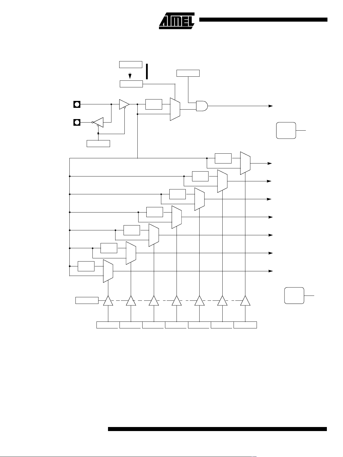
Figure 5. Clock CPU Generation Diagram
XTAL1
XTAL2
÷ 2
PD
PCON.1
÷ 2
1
0
X2B
Hardware byte
X2
CKCON.0
÷ 2
1
0
On RESET
÷ 2
÷ 2
1
0
0
1
÷ 2
1
0
PCON.0
IDL
÷ 2
1
0
÷ 2
1
0
CPU Core
Clock
CLOCK
CPU Core Clock Symbol
and ADC
1
0
FT0 Clock
FT1 Clock
FT2 Clock
FUart Clock
FPca Clock
FWd Clock
FCan Clock
CPU
18
X2
CKCON.0
CANX2
CKCON.7
T89C51CC01
WDX2
CKCON.6
PCAX2
CKCON.5
SIX2
CKCON.4
T2X2
CKCON.3
T1X2
CKCON.2
PERIPH
CLOCK
Peripheral Clock Symbol
T0X2
CKCON.1
Rev. D – 17-Dec-01
Page 19
XTAL1
XTAL2
X2 bit
CPU
T89C51CC01
Figure 6. Mode Switching Waveforms
X2STD STD
Note: In order to prevent any incorrect operation while operating in the X2 mode, users must be
aware that all peripheralsusing the clock frequency as a time reference (UART, timers...)
will have their time reference divided by two. For example a free running timer generating
an interrupt every 20 ms will then generate an interrupt every 10 ms. A UART with a
4800 baud rate will have a 9600 baud rate.
6.2 Register Table 12. CKCON Register
CKCON (S:8Fh)
Clock Control Register
76543210
CANX2 WDX2 PCAX2 SIX2 T2X2 T1X2 T0X2 X2
Bit
Number
7CANX2
6WDX2
5 PCAX2
4SIX2
3T2X2
Bit
Mnemonic Description
CAN clock (1)
Clear to select 6 clock periodsper peripheral clock cycle.
Set to select 12 clock periods per peripheral clock cycle.
Watchdog clock (1)
Clear to select 6 clock periodsper peripheral clock cycle.
Set to select 12 clock periods per peripheral clock cycle.
Programmable Counter Array clock (1)
Clear to select 6 clock periodsper peripheral clock cycle.
Set to select 12 clock periods per peripheral clock cycle.
Enhanced UART clock (MODE 0 and 2) (1)
Clear to select 6 clock periodsper peripheral clock cycle.
Set to select 12 clock periods per peripheral clock cycle.
Timer2 clock (1)
Clear to select 6 clock periodsper peripheral clock cycle.
Set to select 12 clock periods per peripheral clock cycle.
Rev. D – 17-Dec-01
Timer1 clock (1)
2T1X2
Clear to select 6 clock periodsper peripheral clock cycle.
Set to select 12 clock periods per peripheral clock cycle.
19
Page 20

Bit
Number
1T0X2
0X2
Bit
Mnemonic Description
Timer0 clock (1)
Clear to select 6 clock periodsper peripheral clock cycle.
Set to select 12 clock periods per peripheral clock cycle.
CPU clock
Clear to select 12 clock periods per machine cycle (STD mode) for CPU and all
the peripherals.
Set to select6clockperiodspermachine cycle(X2 mode) and to enable the
individual peripherals "X2"bits.
Notes: 1. This control bit is validated when the CPU clock bit X2 is set; when X2 is low, this bit
has no effect.
Reset Value = 0000 0000b
20
T89C51CC01
Rev. D – 17-Dec-01
Page 21

T89C51CC01
7. Data Memory The T89C5 1CC01 provides data memory access in two diffe re nt spac es :
1. The internal space mapped in three separate segments:
• the lower 128 bytes RAM s egment.
• the upper 128 bytes RAM segment.
• the expanded 1024 bytes RAM s egment (ERAM).
2. The external space.
A fourth internal segment is avail able but ded icated to Speci al Function R egisters,
SFRs, (addresses 80h to
Figure 2 shows the internal and exte rn al data m emory spaces organization.
Figure 1. Internal memory - RAM
FFh) accessible by direct addressing mode.
FFh
128 bytes
Internal RAM
indirect addressing
80h
7Fh
128 bytes
Internal RAM
director indirect
00h
addressing
Upper
Lower
FFh
direct addressing
80h
Special
Function
Registers
Figure 2. Internal and External Data Memory Organization E RAM-XRAM
FFFFh
64 Kbytes
External XRAM
Rev. D – 17-Dec-01
256upto1024bytes
Internal ERAM
EXTRAM= 0
00h
Internal
FFh or 3FFh
EXTRAM= 1
0000h
External
21
Page 22
7.1 Internal Space
7.1.1 Lower 128 Bytes RAM The lower 128 by tes of RAM (see Figure 2) are ac cessible from address 00h to 7Fh
using direct or indirect addressing modes. The lowest 32 bytes are grouped into 4 banks
of 8 registers (R0 to R7). Two bits RS0 and RS1 in PSW register (see Fig ure 3) select
which bank is in use according to Table 1. This allows more e fficient use of cod e space,
since register instructions are shorter than instructions that use dir ec t addressing, and
can be used for context switching in interrupt service routines .
Table 1. Register Bank Selection
RS1 RS0 Description
0 0 Register bank 0 from 00h to 07h
0 1 Register bank 0 from 08h to 0Fh
1 0 Register bank 0 from 10h to 17h
1 1 Register bank 0 from 18h to 1Fh
The next 16 bytes above the register banks form a block of bit-addressable memory
space. The C51 inst ruction set includes a wide selectio n of single-bit instructions, and
the 128 bits in this area can be directly addressed by these instructions. The bit
addresses in this area are 00h to 7 Fh.
Figure 3. Lower 128 bytes Internal RAM Organi z ation
7Fh
30h
20h
18h
10h
08h
00h
2Fh
Bit-Addressable Space
(Bit Addresses 0-7Fh)
1Fh
17h
4 Banks of
8Registers
0Fh
R0-R7
07h
7.1.2 Upper 128 Bytes RAM The upper 128 bytes of RAM are a ccessible from address 80h to FFh using only indirect
addressing mode.
7.1.3 Expanded RAM The on-chip 1024 bytes of expanded RAM (ERAM) are ac c es s ible from addres s 0000h
to 03FFh using indirect addressing mode through MOVX instructions. I n this address
range, the bit EXTRAM in AUXR register is used to select the ERAM ( default) or the
XRAM. As s how n in Figure 2 wh en EX TRAM = 0 , the E RAM is se le cte d and wh en
EXTRAM= 1, the XRAM is selected.
The size of ERAM can be configured by XRS1-0 bit in AUXR register (default size is
1024 bytes).
Caution:
Note: Lower 128 bytes RAM, Upper 128 bytes RAM, and expanded RAM are made of volatile
memory cells. This means that the RAM content i s indeterminate after power-up and
must then be initialized properly.
22
T89C51CC01
Rev. D – 17-Dec-01
Page 23
T89C51CC01
7.2 External Space
7.2.1 Memory Interface The external memory in terface comprises the external bus (port 0 and port 2) as well as
the bus control signals (RD#, WR#, and ALE).
Figure 4 shows the structure of the external address bus. P0 carries address A7:0 while
P2 carries address A1 5:8. Data D 7:0 is multiple xe d with A7:0 on P0 . Table 2 des c ribes
the external memory interface signals.
Figure 4. External Data Memory Interface Structure
T89C51CC01
ALE
WR#
P2
P0
AD7:0
A15:8
Latch
A7:0
RAM
PERIPHERAL
A15:8
A7:0
D7:0
OERD#
WR
Table 2. External Data Memory Interface Signals
Signal
Name Type Description
A15:8 O
AD7:0 I/O
ALE O
Address Lines
Upper address lines for the external bus.
Address/Data Lines
Multiplexed lower address lines and data for the external
memory.
Address Latch Enable
ALE signals indicates that valid address information are available
on lines AD7:0.
Alternative
Function
P2.7:0
P0.7:0
-
RD# O
WR# O
Read
Read signal output to external data memory.
Write
Write signal output to external memory.
P3.7
P3.6
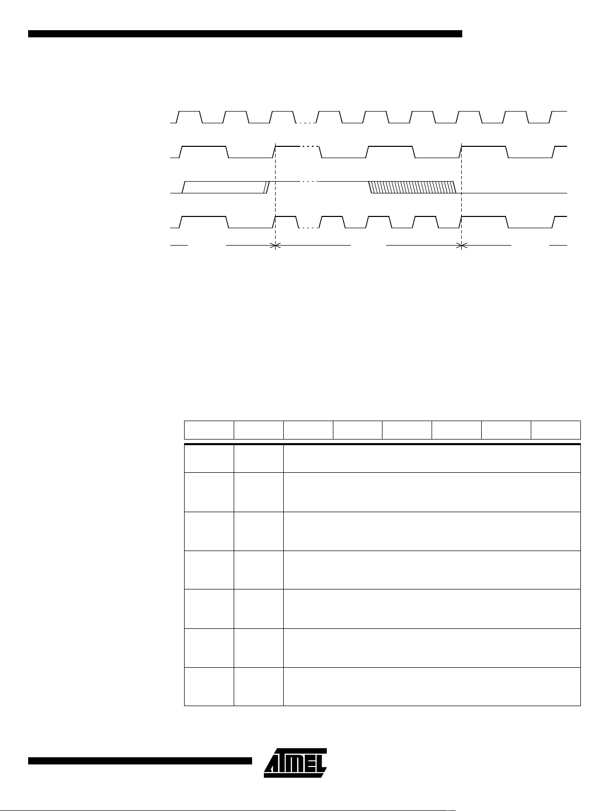
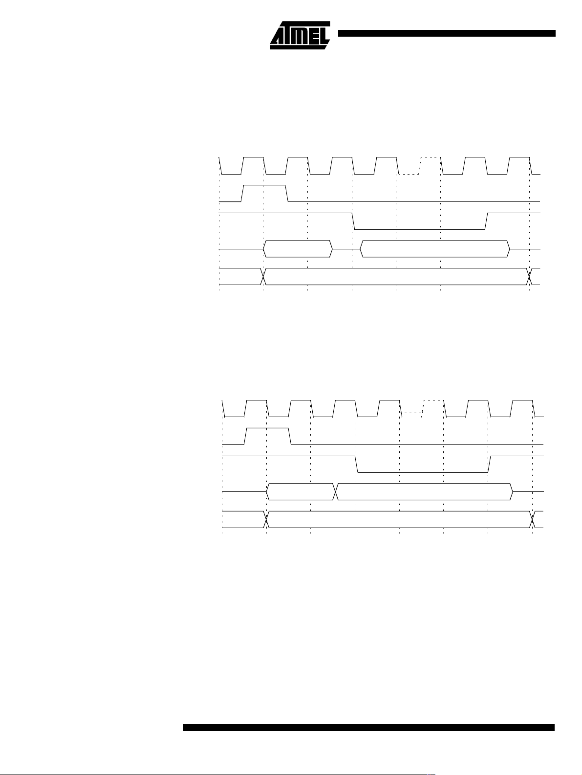
7.2.2 External Bus Cycles This section describes the bu s cycles the T89C51CC01 executes t o read (see Figure 5),
and write data (see Figure 6) in the external data m emory.
External m emory cycle takes 6 CPU c lock periods. This is equivalent to 12 oscillator
clock period in standard mode or 6 oscillator clock periods in X2 mode. For further information on X2 mode.
Slow peripherals can be accessed by stretching the read and write cycles. This is done
using the M0 bit in AUXR register. Setting this bit changes the width of the RD# and
WR# signals from 3 to 15 CPU clock periods.
23
Rev. D – 17-Dec-01
Page 24
For simplicity, the accompanying figures depict the bus cycle waveforms in idealized
form and do not provide precise timing information. For bus cycle timing parameters
refer to the Section “AC Characteristics” of the T89C51CC01 datasheet.
Figure 5. External Data Read Waveforms
CPU Clock
ALE
RD#1
P0
P2
Notes: 1. RD# signal may be stretched using M0 bit in AUXR register.
P2
2. When executing MOVX @Ri instruction, P2 outputs SFR content.
DPL or Ri D7:0
DPH or P22
Figure 6. External Data Write Waveforms
CPU Clock
ALE
WR#1
P0
P2
P2
DPL or Ri D7:0
DPH or P22
Notes: 1. WR# signal may be stretched using M0 bit in AUXR register.
2. When executing MOVX @Ri instruction, P2 outputs SFR content.
7.3 Dual Data Pointer
7.3.1 Description The T89C51CC01 implements a second data pointer for speeding up code execution
and reducing code size in cas e of intensive usage of external m emory accesses.
DPTR0 and DPTR1 are seen by the CPU as DPTR and are accessed using the SFR
addresses 83h and 84h that are the DPH and DPL addresses. Th e DPS bit in AUX R1
register (see Figure 5) is used to select whether DPTR is the data pointer 0 or the dat a
pointer 1 (see Figure 7).
24
T89C51CC01
Rev. D – 17-Dec-01
Page 25
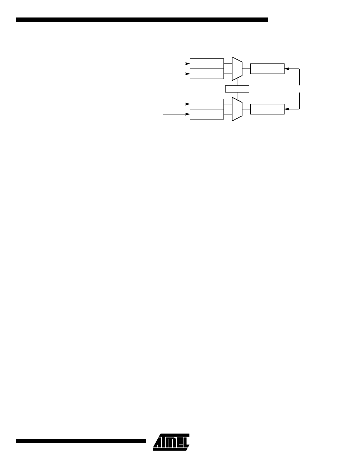
Figure 7. Dual Data Pointer Implementation
T89C51CC01
DPL0
0
DPL
DPL1
DPTR0
DPTR1
DPH0
1
DPS
0
AUXR1.0
DPTR
DPH
DPH1
1
7.3.2 Application Software can take advantage of the additional data pointers to both increase speed and
reduce code size, f or example, block operations ( c opy, compare…) are well served by
using one data pointer as a “source” pointer and the other one a s a “destination” pointer.
Hereafter is an example of block m ove implementation u sing the two pointers and coded
in assembler. The l at est C compi ler takes also advanta ge of this f eature by providin g
enhanced algorithm libraries.
The INC instruction is a short (2 bytes) and fast (6 machin e cycle) way to manipulate the
DPS bit in the AUX R1 register. However, note that the INC instruction does not directly
force the DPS bit to a particular state, but simply toggles it. In simple routines, such as
the block move exam ple, only the fact that DPS is toggled in the proper sequence matters, not its actual value. In other words, the block move routine works the same whether
DPS is '0' or '1' on entry.
; ASCII block move using dual data pointers
; Modifies DPTR0, DPTR1, A and PSW
; Ends when encountering NULL character
; Note: DPS exits opposite to the entry state unless an extra INC AUXR1 is
added
AUXR1EQU0A2h
move:movDPTR,#SOURCE ; address of SOURCE
incAUXR1 ; switch data pointers
movDPTR,#DEST ; address of DEST
mv_loop:incAUXR1; switch data pointers
movxA,@DPTR; get a byte from SOURCE
incDPTR; increment SOURCE address
incAUXR1; switch data pointers
movx@DPTR,A; write the byte to DEST
incDPTR; increment DEST address
jnzmv_loop; check for NULL terminator
end_move:
Rev. D – 17-Dec-01
25
Page 26

7.4 Registers Table 3. PSW Register
PSW (S:8Eh)
Program Status Word Register.
76543210
CY AC F0 RS1 RS0 OV F1 P
AUXR (S:8Eh)
Auxiliary Register
Bit
Number
7CY
6AC
5F0User Definable Flag 0.
4-3 RS1:0
2OV
1F1User Definable Flag 1.
0P
Bit
Mnemonic Description
Carry Flag
Carry out from bit 1 of ALU operands.
Auxiliary Carry Flag
Carry out from bit 1 of addition operands.
Register Bank Select Bits
Refer to Table 1 for bits description.
Overflow Flag
Overflow set by arithmetic operations.
Parity Bit
Set when ACC contains anoddnumber of 1’s.
Cleared when ACC contains an even number of 1’s.
Reset Value= 0000 0000b
Table 4. AUXR Register
26
T89C51CC01
76543210
- - M0 - XRS1 XRS0 EXTRAM A0
Bit
Number
7-6 -
5M0
4-
Bit
Mnemonic Description
Reserved
The valueread from these bits are indeterminate.Donotsetthis bit.
Stretch MOVX control:
the RD/ and the WR/ pulse length isincreasedaccording to the value of M0.
M0 Pulse length in clock period
06
130
Reserved
The value readfrom this bit is indeterminate.Donot set this bit.
Rev. D – 17-Dec-01
Page 27

T89C51CC01
AUXR1 (S:A2h)
Auxiliary Control Register 1.
Bit
Number
3-2 XRS1-0
1 EXTRAM
0A0
Bit
Mnemonic Description
ERAM size:
Accessiblesize of the ERAM
XRS1:0 ERAM size
0 0 256 bytes
0 1 512 bytes
1 0 768 bytes
1 1 1024 bytes (default)
Internal/External RAM (00h - FFh)
access usingMOVX@ Ri / @ DPTR
0 - Internal ERAM access using MOVX @ Ri / @ DPTR.
1 - External data memory access.
Disable/Enable ALE)
0 - ALE is emitted at a constant rateof 1/6 the oscillatorf requency (or 1/3ifX2
mode is used)
1-ALEisactiveonlyduringaMOVXorMOVCinstruction.
Reset Value= X00X 1100b
Not bit addressable
Table 5. AUXR1 Register
76543210
- - ENBOOT - GF3 0 - DPS
Bit
Number
7-6 -
5 ENBOOT
4-
3GF3General Purpose Flag 3.
20
1-Reserved for Data Pointer Extension.
0DPS
Bit
Mnemonic Description
Reserved
The value readfrom these bits is indeterminate. Do not set these bits.
Enable Boot Flash
Set this bit for map the boot flash between F800h -FFFFh
Clearthis bit for disable bootflash.
Reserved
The value readfrom this bit is indeterminate.Donot set this bit.
Always Zero
This bit is stuck to logic 0 to allow INC AUXR1 instruction without affecting GF3
flag.
Data Pointer Select Bit
Set to select second dual data pointer: DPTR1.
Clear to select firstdualdata pointer:DPTR0.
Reset Value= XXXX 00X0b
Rev. D – 17-Dec-01
27
Page 28

8. EEPROM Data
Memory
The 2k byte on-chip EEPROM memory block is located at addresses 0000h to 07FFh of
the XR AM /ERAM memory space and is selected by setting control b its in the EECO N
register. A read in the EEPROM memory is done with a MOVX instruction.
A physical write in the EEPROM memory is done in two steps: write data in the column
latches and transfer of all data latches into an EEPROM memory row (programming).
The number of data written on the page may vary from 1 up to 128 bytes (the page
size). When programming, only the data written in the colum n latch is programmed and
a ninth bit is used to obtain this feature. This provides the capability t o program t he
whole memory by by tes, by page or by a number of b ytes in a page. Indeed, each ninth
bit is set when the writing the corresponding byte in a row and all these ninth bits are
reset after the writing of the complete EEPROM row.
8.1 Write Data in the
column latches
Data is written b y byte to the column latches as for an external RAM memory. Out of the
11 address bits of the data pointer, the 4 MSBs are used for page selection (row) and 7
are u sed for byte selection. Between two EEPROM programming sessions, a ll the
addresses in the column latches must stay on t he same page, meaning that the 4 MSB
must no be change d.
The following procedure is used to write to the column latches:
• Save and disable interrupt.
• Set bit EEE of EECO N regi ster
• Load DPTR with the address to write
• Store A regi ster with the data to be written
• Execute a MOVX @DPTR, A
• If needed loop the three last ins tructions until the end of a 128 bytes page
• Restore interrupt.
Note: The last page address used when loading the column latch is the one used to select the
page programming address.
8.2 Programming The EEPROM programming consists on the following actions:
• writing one or more bytes of one page in the column latches. Normally, all by tes
must belong to the same page; if not, the first page address will be latched and the
others discarded.
• launching programming by writing the control seque nc e (50h followed by A0h) to the
EECON register.
• EEBUSY flag in EECON is then set by hardware to indicate that programming is in
progress and that the EEPROM segment is not available for reading.
• The end of programming is indi ca ted by a hardware clear of the EEBUSY flag.
Note: The sequence 5xh and Axh m ust be executed without instructions between then other-
wise the programming is aborted.
8.3 Read Data The following procedure is used to read the data stored in the EEPROM memory:
• Save and disable interrupt
• Set bit EEE of EECO N regi ster
• Load DPTR with the address to read
• Execute a MOVX A, @DPTR
• Restore interrupt
28
T89C51CC01
Rev. D – 17-Dec-01
Page 29

T89C51CC01
8.4 Examples ;*F*************************************************************************
;* NAME: api_rd_eeprom_byte
;* DPTR contain address to read.
;* Acc contain the reading value
;* NOTE: before execute this function, be sure the EEPROM is not BUSY
;***************************************************************************
api_rd_eeprom_byte:
MOV EECON, #02h; map EEPROM in XRAM space
MOVX A, @DPTR
MOV EECON, #00h; unmap EEPROM
ret
;*F*************************************************************************
;* NAME: api_ld_eeprom_cl
;* DPTR contain address to load
;* Acc contain value to load
;* NOTE: in this example we load only 1 byte, but it is possible upto
;* 128 bytes.
;* before execute this function, be sure the EEPROM is not BUSY
;***************************************************************************
api_ld_eeprom_cl:
MOV EECON, #02h ; map EEPROM in XRAM space
MOVX @DPTR, A
MOVEECON, #00h; unmap EEPROM
ret
;*F*************************************************************************
;* NAME: api_wr_eeprom
;* NOTE: before execute this function, be sure the EEPROM is not BUSY
;***************************************************************************
api_wr_eeprom:
MOV EECON, #050h
MOV EECON, #0A0h
ret
Rev. D – 17-Dec-01
29
Page 30

8.5 Registers Table 6. EECON Register
EECON (S:0D2h)
EEPROM Control Register
76543210
EEPL3 EEPL2 EEPL1 EEPL0 - - EEE EEBUSY
Bit
Bit Number
Mnemonic Description
7-4 EEPL3-0
3-
2-
1 EEE
0 EEBUSY
Programming Launch command bits
Write 5Xh followed by AXh to EEPL to launch the programming.
Reserved
The value read from this bit is indeterminate. Do not set this bit.
Reserved
The value read from this bit is indeterminate. Do not set this bit.
Enable EEPROM Space bit
SettomaptheEEPROMspaceduringMOVXinstructions(Writeinthecolumn
latches)
Clear to map the XRAM space during MOVX.
Programming Busy flag
Set by hardware when programming is in progress.
Cleared by hardwarewhenprogramming is done.
Can not be set or clearedbysoftware.
ResetValue=XXXX XX00b
Not bit addressable
30
T89C51CC01
Rev. D – 17-Dec-01
Page 31

T89C51CC01
9. Program/Code
Memory
The T89C51CC01 implement 32 Kbytes of on-chip program/code memory. Figure 8
shows the partitioning of internal and external program/code memory spaces depending
on the product.
The FLASH memory increases EPROM and ROM functionality by in-circuit electrical
erasure and programming. Thanks to th e internal charge pump, t he high voltage needed
for p rogramming or erasi ng FLAS H cells is g enerated on-chip using the standard VDD
voltage. Th us, the FLA SH Memory can be program med using only on e voltage and
allows In-System Programming commonly known as ISP. Hardware programming mode
is also available using specific p ro gramm ing tool.
Figure 8. Program/Code Memory O rganizat ion
FFFFh
32 Kbytes
external
memory
8000h
7FFFh
32 Kbytes
internal
FLASH
7FFFh
32 Kbytes
external
memory
EA = 1
0000h
Note: If the program executes exclusively from on-chip code memory (not from external mem-
ory), beware of executing code from the upper byte of on-chip memory (7FFFh) and
thereby disrupt I/O Ports 0 and 2 due to external prefetch. Fetching code constant from
this location does not affect Ports 0 and 2.
0000h
EA = 0
9.1 External Code
Memory Access
9.1.1 Memory Interface The external memory in terface comprises the external bus (port 0 and port 2) as well as
the bus control signals (PSEN#, and ALE ).
Figure 9 shows the structure of the external address bus. P0 carries address A7:0 while
P2 carries address A1 5:8. Data D 7:0 is multiple xe d with A7:0 on P0 . Table 7 des c ribes
the external memory interface signals.
Rev. D – 17-Dec-01
31
Page 32

Figure 9. External Code Memory Interface Structure
T89C51CC01
ALE
P2
P0
AD7:0
A15:8
Latch
A7:0
FLASH
EPROM
A15:8
A7:0
D7:0
OEPSEN#
Table 7. External Code Memory Interface Si gnals
Signal
Name Type Description
A15:8 O
AD7:0 I/O
ALE O
PSEN# O
Address Lines
Upper address lines for the external bus.
Address/Data Lines
Multiplexed lower address lines and data for the external memory.
Address Latch Enable
ALE signals indicates that validaddress information are available on lines
AD7:0.
Program Store Enable Output
This signal is activelow during external code fetchorexternalcoderead
(MOVC instruction).
Alternate
Function
P2.7:0
P0.7:0
-
-
9.1.2 External Bus Cycles This section describes the bus cycles the T89C51CC01 executes to fetch code (see
Figure 10) in the external program/cod e memory.
External m emory cycle takes 6 CPU c lock periods. This is equivalent to 12 oscillator
clock period in standard mode or 6 oscillator clock periods in X2 mode. For further information on X2 mode see s ec tion “Clock “.
For simplicity, the accom panying figure de picts the bus cycle waveforms in idealized
form and do not provide precise timing in formation.
For bus cycling parameters refer to the section "AC-DC parameters".
32
T89C51CC01
Rev. D – 17-Dec-01
Page 33

Figure 10. External Code Fetch Waveforms
CPU Clock
ALE
PSEN#
T89C51CC01
9.2 FLASH Memory
Architecture
D7:0
P0
P2
T89C51CC01 features two on-c hip f lash memories:
• Flash memory FM0:
containing 32 Kbytes of program memory (user space) organized into 128 byte
pages,
• Flash memory FM1:
2 Kbytes for boot loader and Application Programming Interfaces (API).
The FM0 c an be program by both parallel programming and S erial In-System Programming (ISP) whereas FM1 supports only parallel programmi ng by programmers. The ISP
mode is detailed in the "In-System P rogramming" section.
All Read/Write access operations on FLASH Memory by user application are managed
by a set of API described in the "In-System Programming" section.
Figure 11. Flash memory architecture
Hardware Security (1 byte)
Extra Row (128 bytes)
Column Latches (128 bytes)
PCL
PCLD7:0 D7:0
PCHPCH
PCH
2Kbytes
Flash memory
boot space
FM1
FFFFh
F800h
Rev. D – 17-Dec-01
7FFFh
0000h
32 Kbytes
Flash memory
user space
FM0
FM1 mapped between FFFFh and
F800h when bit ENBOOT is set in
AUXR1 register
33
Page 34

9.2.1 FM0 Memory
Architecture
The flash memory is made up o f 4 b locks (see Figure 11):
3. The memory array (user space) 32 Kbytes
4. The Extra Row
5. The Hardware security bits
6. The column latch registers
User Space This space is compo se d of a 32 Kbytes FLASH memory organized in 256 pages of 1 28
bytes. It contains the user’s application code.
Extra Row (X Row) This row is a part of FM0 and has a s ize of 128 bytes . The extra row may contain infor-
mation for boot loader usage.
Hardware security Byte The Hardware security Byte space is a part of FM0 and has a size o f 1 byte.
The 4 MS B can be read/written by soft w are, the 4 LSB can only be read by sof t w are and
written by hardware in parallel mode.
Column latches The column latches, also part of FM0, have a size of full page (128 bytes).
The column latches are the entrance buffers of the three previous memory locations
(user array, XROW and Hardware security byte).
9.2.2 Cross Flash Memory
Access Description
The FM0 memory can be program only from FM1. Programming FM0 from FM0 or from
external memory is impossible.
The FM1 memory can be program only by parallel programming.
The Table 8 show all software f lash access allowed.
Table 8. Cross Flash Memory Access
Code executing from
FM0
(user Flash)
FM1
(boot flash)
External
memory
EA = 0
Action
Read ok -
Load column latch ok -
Write - -
Read ok ok
Load column latch ok -
Write ok -
Read - -
Load column latch - -
Write - -
FM0
(user Flash)
FM1
(boot Flash)
34
T89C51CC01
Rev. D – 17-Dec-01
Page 35

T89C51CC01
9.3 Overview of FM0
operations
9.3.1 Mapping of the memor y
space
The CPU interfaces to the flash memory through the FCON register and AUXR1
register.
These registers are used to:
• Map the memory spaces in the adressable space
• Launch the programming of the memory spaces
• Get the status of the flash memory (bus y /not busy)
By default, the user space is accessed by MOVC instruction for re ad only. The c olumn
latches space is m a de accessible by setting the FPS bit in FCON register. Writing is
possible from 0000h to 7FFFh, address bits 6 to 0 are used to select an address within a
page while bits 14 to 7 are used to sele ct the programming address of the page.
Setting FPS bit takes precedence on the EXTRAM bit in AUXR register.
The o th er memory spaces (user, extra row, hardw are security) are made acc es s ible in
the code segment b y program ming bits FMOD0 and FMOD1 in FCON register in accordance with Table 9. A MOVC instruction is then used for reading these spaces.
Table 9. .FM0 blocks select bits
FMOD1 FMOD0 FM0 Adressable space
0 0 User (0000h-FFFFh)
0 1 Extra Row(FF80h-FFFFh)
1 0 Hardware Security Byte (0000h)
11reserved
9.3.2 Launching programming FPL3:0 bits in FCON register are used to secure the launch of programming. A specific
sequence must be written in these bits to unl oc k the write protection and t o launch the
programming. This sequence is 5xh followed by Axh. Table 10 summarizes the memory
spaces to program according to F MOD1:0 bits.
Rev. D – 17-Dec-01
35
Page 36

Table 10. Programming spaces
Write to FCON
5 X 0 0 No action
User
AX00
5 X 0 1 No action
Extra Row
AX01
OperationFPL3:0 FPS FMOD1 FMOD0
Write the column latches in user
space
Write the column latches in extra row
space
9.3.3 Status of the flash
memory
Hardware
Security
Byte
Reserved
Note: The sequence 5xh and Axh must be executing without instructions between them other-
wise the programming is aborted.
Note: Interrupts that may occur during programming time must be disabled to avoid any spuri-
ous exit of the programming mode.
The bit FBUSY in FCON register is used t o indicat e the s ta tus of program ming.
FBUSY is set when programmi ng is in progress.
5 X 1 0 No action
A X 1 0 Write the fuse bits space
5 X 1 1 No action
A X 1 1 No action
9.3.4 Selecting FM1 The bit ENBOOT in AUXR1 register is used to map FM1 from F800h to FFFFh.
9.3.5 Loading the Column
Latches
Any number of data from 1 byte to 128 bytes can be loaded in the column latches. This
provides the capability to program the whole memory by byte, by page or by any number
of bytes in a page.
When programming is launched, an automatic erase of the locations loaded in the column latches is first performed, then programming is effectively done. Thus no page or
block erase is needed an d only the loaded data are programmed in the corresponding
page.
36
The fol lowi ng p ro ced ur e is u se d to l oa d th e co lu mn latches a nd i s su mm a rized in
Figure 12:
• Disable interrupt and map the column latch space by setting FPS bit.
• Load the DPTR with the address t o load.
• Load Accumulator register wi th th e da ta to load.
• Execute the MOVX @DPTR, A instruction.
• If needed loop the three last ins tructions until the page is completely loaded.
• unmap the column latch and Enable Interrupt
T89C51CC01
Rev. D – 17-Dec-01
Page 37

Figure 12. Column Latches Loading Procedure
Column Latches
Loading
Save & Disable IT
EA= 0
Column Latches Mapping
FCON = 08h (FPS=1)
Data Load
DPTR= Address
ACC= Data
Exec:MOVX@DPTR,A
Last Byte
to load?
T89C51CC01
Data memory Mapping
FCON = 00h (FPS = 0)
Restore IT
Note: The last page address used when loading the column latch is the one used to select the
page programming address.
9.3.6 Program m in g the FLASH
Spaces
User The followi ng pro ced ure is used to pro gram the User spa ce and is s um mar ize d in
Figure 13:
• Load up to one page of data in the column latches from address 0000h to 7FFFh.
• Disable the interrupts.
• Launch the programming by writing the data sequence 50h followed by A0h in
FCON register (only from FM1).
The end of the programming indicated by the FBUSY flag cleared.
• Enable the interrupts.
Extra Row The following proc edure is used to program the Ex tra Row space and is summ arized in
Figure 13:
• Load data in the column latches from address FF80h to FFFFh.
• Disable the interrupts.
Rev. D – 17-Dec-01
37
Page 38

• Launch the programming by writing the data sequence 52h followed by A2h in
FCON register (only from FM1).
The end of the programming indicated by the FBUSY flag cleared.
• Enable the interrupts.
Figure 13. Flash and Extra row Programming Procedure
FLASH Spaces
Programming
Column Latches Loading
see Figure 12
Save & Disable IT
EA= 0
Launch Programming
FCON= 5xh
FCON= Axh
Hardware Security Byte
FBusy
Cleared?
Clear Mode
FCON = 00h
End Programming
Restore IT
The following procedure is used to program the Hardware Security Byte space
and is summarizedin Figure 14:
• Set FPS and map Hardware byte (F CON = 0x0C)
• Save and disable the interrupts.
• Load DPTR at address 0000h.
• Load Accumulator register wi th th e da ta to load.
• Execute the MOVX @DPTR, A instruction.
• Launch the programming by writing the data sequence 54h followed by A4h in
FCON register (only from FM1).
The end of the programming indicated by t he FBusy flag cleared.
• Restore the interrupts
38
.
T89C51CC01
Rev. D – 17-Dec-01
Page 39

Figure 14. Hardware Programming Procedure
FLASH Spaces
Programming
Save & Disable IT
EA= 0
FCON = 0Ch
T89C51CC01
Save & Disable IT
EA= 0
Launch Programming
FCON= 54h
FCON= A4h
Data Load
DPTR= 00h
ACC= Data
Exec:MOVX@DPTR,A
End Loading
Restore IT
FBusy
Cleared?
Clear Mode
FCON = 00h
End Programming
RestoreIT
9.3.7 Reading the FLASH
Spaces
User The following procedure is used to read t he User space:
• Read one byte in Ac cu mulator by executing MOVC A,@A+DPTR with
A+DPTR=read@.
Note: FCON is supposed to be reset when not needed.
Extra Row The following proc edure is used to read the Extra Row space and is summarized in
Figure 15:
• Map the Extra Row space by writing 02h in FCON register.
• Read one byte in Ac cu mulator by executing MOVC A,@A+DPTR with A= 0 &
DPTR= FF80h to FFFFh.
• Clear FCON to unmap the Extra Row.
Hardware Security Byte
Rev. D – 17-Dec-01
The fo llowing pro c ed ur e is used to re ad the Hardwar e Security space a nd is
summarized in Figure 15:
• Map the Hardware Secur ity space by writing 04h i n FC ON register.
• Read the byte in Accumulator by executing MOVC A,@A+DPTR with A= 0 &
DPTR= 0000h.
• Clear FCON to unm ap the H ardware Security Byte.
39
Page 40

Figure 15. Reading Procedure
FLASH Spaces
Reading
FLASH SpacesMapping
FCON= 00000xx0b
Data Read
DPTR= Address
Exec:MOVCA,@A+DPTR
ACC= 0
Clear Mode
FCON = 00h
9.3.8 Flash Protection from
Parallel Programming
The three lock bits in Hardware Security Byte (see "In-System Programmi ng" section)
are program med according to Tabl e 11 provide differe nt level of pro te c t ion f or the onchip code and data located in FM0 and FM1.
The only way to write this bits are the parallel mode. They are set by default to level 4
Table 11. Program Lock bit
Program Lock Bits
Security
level
1UUU
2PUU
3UPU
4 UUP
LB0 LB1 LB2
Protection description
No program lock features enabled. MOVC instruction executed from
external program memory returns non encrypted data.
MOVC instruction executed from external program memory are
disabled from fetching code bytes from internal memory, EA
and latched on reset, and further parallel programming of the Flash is
disabled.
Same as 2, also verify throughparallelprogramming interface is
disabled.
Same as 3, also external execution is disabled if code roll over beyond
7FFFh
is sampled
Program Lock bits
40
U: unprogrammed
P: programmed
WARNING: Security level 2 and 3 should only be programmed after F lash and Core
verification.
T89C51CC01
Rev. D – 17-Dec-01
Page 41

9.4 Registers
FCON RegisterFCON (S:D1h)
FLASH Control Re gister
T89C51CC01
76543210
FPL3 FPL2 FPL1 FPL0 FPS FMOD1 FMOD0 FBUSY
Bit
Number
7-4 FPL3:0
3FPS
2-1 FMOD1:0
0 FBUSY
Bit
Mnemonic Description
Programming Launch Command Bits
Write 5Xh followed by AXh to launch the programming according to FMOD1:0.
(see Table 10.)
FLASH Map Program Space
Set to map the column latch space in the data memory space.
Clear to re-map the data memory space.
FLASH Mode
See Table 9 or Table 10.
FLASH Busy
Set by hardware when programming is in progress.
Clearbyhardwarewhen programming is done.
Can not be changed by software.
Reset Value= 0000 0000b
Rev. D – 17-Dec-01
41
Page 42

10. In-System-
Programming (ISP)
With the implementation of the User Space (FM0) and the Boot Space (FM1) in Flash
technology the T89C51CC01 allows the system engineer the develop m ent of applications with a very high level of flexibility. This flexibility is based on the possibility to alter
the customer program at any st ages of a product’s life:
• Before assembly the 1st personalization of the product by programming in the FM 0
and if needed also a customized Boot loader in the FM1.
Atmel provide also a standard Boot loader by default UART or CAN.
• After assembling on the PCB in its final embedded position by serial mode via the
CAN bus or UART.
This In-System-Programming (ISP) allows code modifica tion over the total lifetim e of the
product.
Besides the default Boot loader Atmel provide to the custo mer also all the needed Application-Programming-Interfaces (API) which are needed for the ISP. The API are located
also in the Boot memo r y.
This allow the customer to have a full use of the 32 Kbyte user m emory.
10.1 Flash Programming
and Erasure
There are three methods of program min g the Fl as h memory:
• The Atmel bootloader l ocated in FM1 is activated by the appl ication. Low level API
routines (located in FM1)will be used to program FM0. The interf ac e used f or seria l
downloading to FM0 is the UART or the CAN. API can be c alle d also by user’s
bootloader located in FM0 at [SBV ]00h.
• A further method exist in activating the Atmel boot loader by hardware activation.
• The FM0 can be pro gramm ed also by the parallel mode using a programmer.
Figure 16. Flash Memory Mapping
FFFFh
2KbytesIAP
bootloader
F800h
7FFFh
Custom
Boot Loader
[SBV]00h
FM1
FM1 mapped b etween F800h and FFFFh
when API called
42
32 Kbytes
Flash memory
FM0
0000h
T89C51CC01
Rev. D – 17-Dec-01
Page 43

10.2 Boot Process
T89C51CC01
10.2.1 Software boot process
example
10.2.2 Hardware boot proces s At the falling edge of RESET, the bit ENBOOT in AUXR1 register i s initialized with the
Many algorithms can be used for the software boot process. Before de scribing them,
We give below the descript ion of t he different flags and bytes.
Boot Loader Jump Bit (BLJB):
- This bit indicates if on R ESET the user wants to jump to this application at address
@0000h on FM0 or exec ute the boot loader at address @F 800h on FM1.
- BLJB = 0 on parts delivered with bootloader programmed.
- To read or modify this bit, the APIs are used.
Boot VectorAddress (SBV):
- This byte contains the MSB of the user boot loader address in F M0.
- The default value of SBV is FFh (no user boot loader in FM 0).
- To read or modify this byte, the AP Is are used.
Extra Byte (EB) & Boot Status Byte (BSB):
- These bytes are reserved for customer use.
- To read or modify these bytes, the APIs are used.
value of Boot Loader Jump Bit (BLJB).
Further at the falling edge of RESET if the following conditions (called H ardware condi-
tion) are detected:
• PSEN low,
• EA high,
• ALE high (or not connected).
– After Hardware Condition t he FCON register is initialized with the value 00h
and the PC is initialized with F800h (FM1).
The Hardware condition mak es the bootloader to be executed, whatever BLJB value is.
If no hardware condition is detected, the F CON register is initialized with the value F0h.
Check of the BLJB value.
•IfbitBLJB=1:
User application in FM0 will be started at @0000h (standard reset).
•IfbitBLJB=0:
Boot loader will be started at @F800h in FM1.
Rev. D – 17-Dec-01
43
Page 44

Figure 17. Hardware Boot Process Algorithm
Hardware
ENBOOT = 0
PC = 0000h
No
RESET
Hardware
condition?
No
BLJB = = 0
?
Yes
bit ENBOOT in AUXR1 register
is initialized with BLJB.
ENBOOT = 1
PC = F800h
FCON = 00h
Yes
FCON = F0h
ENBOOT = 1
PC = F800h
Software
10.3 ApplicationProgramming-Interface
Application
in FM0
Several Application Program Interface (API) cal ls are availa ble for use by an application
program to permit selective erasing and programming of FLASH pages. A ll calls are
made by functions.
All these APIs are describe in an doc umentation: "In-System Programing: F lash Library
for T89C51CC01".
This is available on the web site.
Boot Loader
in FM1
44
T89C51CC01
Rev. D – 17-Dec-01
Page 45

T89C51CC01
Table 12. List of API
API CALL Description
PROGRAM DATA B YTE Writea byte in flashmemory
PROGRAM DATA PAGE Write a page (128 bytes) in flash memory
PROGRAM EEPROM BYTE Write a byte in Eeprom memory
ERASE BLOCK Erase all flash memory
ERASE BOOT VECTOR (SBV) Erase the boot vector
PROGRAM BOOT VECTOR (SBV) Write the boot vector
PROGRAM EXTRA BYTE (EB) Write the extra byte
READ DATA BYTE
READ EEPROM BYTE
READ FAMILY CODE
READ MANUFACTURER CODE
READ PRODUCT NAM E
READ REVISION NUMBER
READ STATUS BIT (BSB) Read the status bit
READ BOOT VECTOR (SBV) Read the boot vector
READ EXTRA BYTE (EB) Read the extra byte
PROGRAM X2 Write the hardware flag for X2 mode
READ X2 Read the hardware flag for X2 mode
PROGRAM BLJB Write the hardware flag BLJB
READBLJB ReadthehardwareflagBLJB
10.4 XROW Bytes Table 13. Xrow mapping
Description Default value Address
Copy of theManufacturer Code 58h 30h
Copy of the Device ID#1: Family code D7h 31h
Copy of theDevice ID#2: Memories size and type F7h 60h
Copy of theDevice ID#3:Name andRevision FFh 61h
Rev. D – 17-Dec-01
45
Page 46

10.5 Hardware Security Byte
Table 14. Hardware Security byte
76543210
X2B BLJB - - - LB2 LB1 LB0
Bit
Number
7X2B
6BLJB
5-3 -
2-0 LB2:0 Lock Bits
Bit
Mnemonic Description
X2 Bit
Set this bit to start in standard mode
Clearthis bit to startinX2mode.
Boot Loader JumpBit
- 1: T o start the user’s application on next RESET (@0000h) located in FM0,
- 0: To startthe boot loader(@F800h) locatedin FM1.
Reserved
The valueread from these bits are indeterminate.
Default value after erasing chip: FFh
Note: Only the 4 MSB bits can be accessed by software.
Note: The 4 LSB bits can only be accessed by parallel mode.
46
T89C51CC01
Rev. D – 17-Dec-01
Page 47

T89C51CC01
11. Serial I/O Port The T89C51CC01 I/O serial port is compatible with the I/O serial port in the 80C52.
It prov ides bot h synch ronous and asynchronous communication modes. It operates as a
Universal Asynchronous Receiver and Transmitter (UART) in three full-duplex modes
(Modes 1, 2 and 3). Asynchronous transmission and reception can occur simultaneously
and at different baud rates
Serial I/O port includes the following enhancements:
• Framing error detection
• Automatic address recognition
Figure 18. Serial I /O Port Block Diagram
IB Bus
11.1 F raming Error Detection
TXD
RXD
SBUF
Transmitter
Write SBUF
Mode0Transmit
RI
TI
SBUF
Receiver
Receive
Shift register
Read SBUF
Load SBUF
Serial Port
Interrupt Request
Framing bit error de tection is provided for the three asynchronous modes. To enable the
framing bit error detection feature, set SMOD0 bit in PCO N register.
Figure 19. Framing Error Block Diagram
RITIRB8TB8RENSM2SM1SM0/FE
Rev. D – 17-Dec-01
Set FE bit if stop bit is 0 (framing error)
SM0toUARTmodecontrol
IDLPDGF0GF1POF-SMOD0SMOD1
To UART framing error control
When t his feature is enabl ed, the rec eiver checks each incoming data frame for a valid
stop bit. An invalid stop bit may result from noise on the serial lines or from simultaneous
transmission by two CPUs. If a valid stop bit is n ot found, the Framing Error bit (FE) in
SCON register bit is set.
The software may examine the FE bit after each reception to check for data errors.
Once set, o nly software or a reset clears the FE bit. Subsequently received frames with
47
Page 48

valid stop bits cannot clear the FE bit. When t he FE feature is enabled, RI rises on the
stop bit instead of the last data bit (See Figure 20. and Figure 21.).
Figure 20. UART Timing in Mode 1
RXD
Data byte
RI
SMOD0=X
FE
SMOD0=1
Start
bit
Figure 21. UART Timing in Modes 2 and 3
RXD
Start
bit
RI
SMOD0=0
RI
SMOD0=1
FE
SMOD0=1
D7D6D5D4D3D2D1D0
Stop
bit
D8D7D6D5D4D3D2D1D0
Data byte Ninth
bit
Stop
bit
11.2 Automatic Address Recognition
48
T89C51CC01
The automatic address recognition f eature is enabled when the multipro ce ssor c ommunication feature is enabled (SM2 bit in SCON register is set).
Implemented in the hardware, automatic address recognition enhances the multiprocessor communication feature by allowing the serial port to examine the address of each
incoming command frame. Only when the serial port recognizes its own address will the
receiver set the RI bit in the SCO N register to generate an interrupt. This ensures that
the CPU is not interrupted by command frames addressed to other devices.
If neces s ary, you can enable the automatic add ress recognition feature in mode 1. In
this configuration, the stop bit takes the place of the ninth data bit. Bit RI is set only when
the re c eived command frame address matches the device’s address and is termina ted
by a valid stop bit.
To support automatic address recognition, a device is identified by a given address and
a broadcast address.
Note: The multiprocessor communication and automatic address recognition features cannot
be enabled in mode 0 (i.e. settingSM2 bit in SCON register in mode 0 has no effect).
Rev. D – 17-Dec-01
Page 49

T89C51CC01
11.3 Given Address Each device ha s an individual add ress that is specified in the SAD DR register; the
SADEN register is a mas k byte that contains don’t -c are bit s (defined by zeros) to form
the dev ice’s given address. The don’t-care bits pro v ide the flexibility to address one or
more slaves at a time. The following example illustrates how a given address is formed.
To address a device by its individual address, the SADEN mask byte must be 1111
1111b.
For example:
SADDR0101 0110b
SADEN
1111 1100b
Given0101 01XXb
Here is an example of how to use given addresses to address different slaves:
Slave A:SADDR1111 0001b
SADEN
1111 1010b
Given1111 0X0Xb
Slave B:SADDR1111 0011b
SADEN
1111 1001b
Given1111 0XX1b
Slave C:SADDR1111 0010b
SADEN
1111 1101b
Given1111 00X1b
The SADEN byte is se lecte d so that each slave may be addressed separately.
For slave A, b it 0 (the LSB) is a don’t-care bit; for slaves B and C, bit 0 is a 1. To communicate with slave A only, the master must send an address where bit 0 is clear (e.g.
1111 0000b).
For s lave A, bit 1 is a 0; for slaves B and C, bit 1 is a don’t care bit. To communicate with
slaves A and B , but not slave C, the master must send an address with bits 0 and 1 both
set (e.g. 1111 0011b).
To c ommunicate with slaves A, B and C, the master must s end an address with bit 0 set,
bit 1 clear, and bit 2 clear (e.g. 1111 0001b).
11.4 Broadcast Address A broadcast address is formed from the logical OR of the SADDR and SADEN regi sters
with zeros defined as don’t-care bits, e.g.:
SADDR 0101 0110b
SADEN 1111 1100b
SADDR OR SADEN1111 111Xb
The use of don’t- care bits provides flexibility in defining the broadcast address, however
in mos t applications, a broadcast address is FFh . The following is an example of using
broadcast addresses:
Slave A:SADDR1111 0001b
SADEN
1111 1010b
Given1111 1X11b,
Slave B:SADDR1111 0011b
SADEN
1111 1001b
Given1111 1X11B,
Rev. D – 17-Dec-01
Slave C:SADDR=1111 0010b
SADEN
1111 1101b
Given1111 1111b
49
Page 50

For slaves A and B, bit 2 is a don’t care bit; for slave C, bit 2 is set. T o communicat e with
all of the slaves, the master must send an address FFh. To communicate with slaves A
and B, but not slave C, the master can send and addre ss FB h.
11.5 Registers Table 15. SCON Regist er
SCON (S:98h)
Serial Control Register
76543210
FE/SM0 SM1 SM2 REN TB8 RB8 TI RI
Bit
Number
7FE
6SM1
5SM2
4REN
3TB8
2RB8
Bit
Mnemonic Description
SM0
Framing Error bit (SMOD0=1)
Cleartoresettheerrorstate,notclearedbyavalidstopbit.
Set by hardware when an invalid stop bit is detected.
Serial port Mode bit 0 (SMOD0=0)
Refer to SM1for serial portmodeselection.
Serial port Mode bit 1
SM0
0 0 ShiftRegister F
0 1 8-bit UART Variable
10 9-bitUARTF
1 1 9-bit UART Variable
Serial port Mode 2 bit / Multiprocessor Communication Enable bit
Clearto disable multiprocessor communication feature.
Set to enable multiprocessor communication feature in mode 2 and 3.
ReceptionEnablebit
Clearto disable serial reception.
Set to enable serial reception.
Transmitter Bit 8 / Ninth bit to transmit in modes 2 and 3
Clearto transmit a logic0 in the 9thbit.
Set to transmit a logic 1 in the 9th bit.
Receiver Bit 8 / Ninth bit received in modes2 and 3
Cleared by hardwareif9th bit receivedisalogic 0.
Set by hardware if 9th bit received is a logic 1.
SM1 Mode Baud Rate
/12 (or F
XTAL
/64 or F
XTAL
/6 in mode X2)
XTAL
/32
XTAL
50
T89C51CC01
TransmitInterrupt flag
1TI
0RI
Clear to acknowledgeinterrupt.
Set by hardware at the end of the 8th bit time in mode 0 or at the beginning of the
stop bit in theother modes.
Receive Interrupt flag
Clear to acknowledgeinterrupt.
Set by hardware at the end of the 8thbittime in mode 0, see Figure 20.and
Figure 21. in the other modes.
Reset Value = 0000 0000b
Bit addressable
Rev. D – 17-Dec-01
Page 51

SADEN (S:B9h)
Slave Address Mask Register
T89C51CC01
Table 16. SADEN Register
76543210
SADDR (S:A9h)
Slave Address Register
Bit
Number
7-0 Mask Data for Slave Individual Address
Bit
Mnemonic Description
Reset Value = 0000 0000b
Not bit addressable
Table 17. SADDR Register
76543210
Bit
Number
7-0 SlaveIndividualAddress
Bit
Mnemonic Description
Reset Value = 0000 0000b
Not bit addressable
Table 18. SBUF Register
SBUF (S:99h)
Serial Data Buffer
Rev. D – 17-Dec-01
76543210
Bit
Number
7-0 Data sent/received by Serial I/O Port
Bit
Mnemonic Description
Reset Value = 0000 0000b
Not bit addressable
51
Page 52

PCON (S:87h)
Power Control Register
Table 19. PCON Register
76543210
SMOD1 SMOD0 - POF GF1 GF0 PD IDL
Bit
Number
7SMOD1
6SMOD0
5-
4POF
3GF1
2GF0
1PD
0IDL
Bit
Mnemonic Description
Serial port Mode bit 1
Settoselectdoublebaudrateinmode1,2or3.
Serial port Mode bit 0
Clear to select SM0 bit in SCON register.
Set to select FE bit in SCON register.
Reserved
The value readfrom this bit is indeterminate.Donot set this bit.
Power-Off Flag
Clear to recognize nextreset type.
Set by hardware when VCC risesfrom 0 to its nominal voltage. Can also be set
by software.
General purpose Flag
Cleared by user for general purpose usage.
Set by user for general purpose usage.
General purpose Flag
Cleared by user for general purpose usage.
Set by user for general purpose usage.
Power-Down mode bit
Cleared by hardwarewhenreset occurs.
Set to enter power-down mode.
Idle mode bit
Clear by hardware when interrupt or reset occurs.
Set to enter idle mode.
52
Reset Value = 00X1 0000b
Not bit addressable
T89C51CC01
Rev. D – 17-Dec-01
Page 53

T89C51CC01
12. Timers/Counters The T89C51CC01 implements two general-purpo s e, 16-bit Timers/Counters. S uc h are
identified as Timer 0 and Ti mer 1, and can b e independe ntly configured to operate in a
variety of mode s as a Time r or an eve nt Count e r. When op erating as a T ime r, the
Timer/Counter ru ns for a p rogrammed length of t ime, th en issues an interrupt request.
When operating as a Counter, the Timer/Counter counts negative t ransitions on an
external pin. After a preset numbe r of counts, the Counter issues an interrupt request.
The various o perat ing modes of each Timer/Coun ter are described in the following
sections.
12.1 Timer/Counter Operations
A basic operation is Timer registers THx and TLx (x= 0, 1) co nnected in casc ade to form
a 16-bit Timer. Setting the run co nt rol bit (TRx) in TCON register (see Figure 20) turns
the Timer on by allowing the selected input to increment TLx. When TLx overflows it
increments THx; when THx overflows it sets the Timer overflow flag (TFx) in TCON register. Settin g the TRx does not clear the THx and TLx Timer registers. T im er registers
can be accessed to obtain the current count or to enter preset value s. They can be read
at any time but TRx b it mus t be cleared to preset their values, otherwi se the behavior of
the Timer/Counter is unpre dicta ble.
The C/Tx# control bit selects Timer operation or Counter operation by selecting the
divided-down peripheral clock or external pin Tx as the source for the counted signal.
TRx bit must be cleared when changing the mode of operation, otherwise the behavior
of the Timer/Counter is unpredict able.
For T im er op eration (C/Tx#= 0), the Timer register counts the divided-down peripheral
clock. The Timer register is incremented once every peripheral cycle (6 peripheral clock
periods). The Timer clock rate is F
/6,i.e.F
PER
/ 12 in standard mode or F
OSC
OSC
/6in
X2 mode.
For Count er operation ( C/Tx#= 1), the Timer register counts the negative transitions on
the Tx external input pin. The e xterna l input is sa m pled every pe riphera l cycles. When
the sample is high in one cycle and low in the next one, the Counter is incremented.
Since it takes 2 cycl es (12 peripheral clock periods) to re cogn ize a negative transition,
the maximum count rate is F
/ 12, i.e. F
PER
/ 24 in standard mode or F
OSC
/12inX2
OSC
mode. There are no restrictions on the duty c ycle of the external input s ignal, but to
ensure that a g iven level is sampled at least onc e before it changes, it s hould be held for
at least one full peripheral cycle.
12.2 Timer 0 Timer 0 functions as either a Timer or event Counter in four modes of operation.
Figure 22 to Figure 25 show the logical configuration of each mode.
Timer 0 is controlled by the four lowe r bits of TMO D register (see Figure 21) and bits 0,
1, 4 and 5 of TCON r egister (see Figure 20). TMOD register selects the method of Timer
gating (GATE0 ), Timer or Counter opera tion (T/C0#) and mo de of operati on (M1 0 and
M00). TCON register provides T ime r 0 c ontrol func t ions: overflow flag (TF0), run control
bit (TR0), interrupt flag (IE0) and interrupt type control bit (IT0).
For normal T im er operat ion (GATE0= 0) , setting TR0 allows TL0 to be incremented by
the selected input. Settin g GATE0 and TR0 allows external pin INT0# to control Tim er
operation.
Timer 0 overflow (count rolls over from all 1s to all 0s) sets TF0 flag generating an interrupt request.
It is important to stop Timer/Counter before changing mode.
12.2.1 Mode 0 (13-bit Timer) Mode 0 c onfigures Timer 0 as an 13-bit Timer which is set up as an 8-bit Timer (TH0
register) with a modulo 32 prescaler implemented with the lower five bits of TL0 register
(see Figure 22). The uppe r three bi ts of TL0 reg ister are indeterminate and should be
ignored. Prescaler overflow increments TH0 register.
53
Rev. D – 17-Dec-01
Page 54

see section “Clock”
Figure 22. Timer/Counter x (x= 0 or 1) in Mode 0
FTx
CLOCK
÷ 6
0
1
THx
(8 bits)
TLx
(5 bits)
Overflow
TFx
TCON reg
Timer x
Interrupt
Request
Tx
C/Tx#
TMOD reg
INTx#
GATEx
TMOD reg
TRx
TCON reg
12.2.2 Mode 1 (16-bit Timer) Mo de 1 configure s Timer 0 as a 16-bit Timer with TH0 and TL 0 registers connected in
cascade (see Figure 23). The s elect ed i nput increments TL0 register.
Figure 23. Timer/Counter x (x= 0 or 1) in Mode 1
see section “Clock”
FTx
CLOCK
Tx
INTx#
÷ 6
0
1
C/Tx#
TMOD reg
THx
(8 bits)
TLx
(8 bits)
Overflow
TFx
TCON reg
Timer x
Interrupt
Request
GATEx
TMOD reg
12.2.3 Mode 2 (8-bit Timer with
Auto-Reload)
see section “Clock”
FTx
CLOCK
Tx
INTx#
GATEx
TMOD reg
TRx
TCON reg
Mode 2 configures Timer 0 as an 8-bit Timer (TL0 register) that automatically reloads
from TH0 register (see Figure 24). TL0 overflow sets TF0 flag in TCON register and
reloads TL0 with the contents of TH0, which is preset by software. When the interrupt
request is serviced, hardware clears TF0. The reload leaves TH0 unchanged. The next
reload value may be changed at any time by writing it to TH0 register.
Figure 24. Timer/Counter x (x= 0 or 1) in Mode 2
÷ 6
0
1
C/Tx#
TMOD reg
TCON reg
TRx
TLx
(8 bits)
THx
(8 bits)
Overflow
TFx
TCON reg
Timer x
Interrupt
Request
54
T89C51CC01
Rev. D – 17-Dec-01
Page 55

T89C51CC01
12.2.4 Mode 3 (Two 8-bit
Timers)
FTx
CLOCK
T0
INT0#
FTx
CLOCK
see section “Clock”
GATE0
TMOD.3
Mode 3 configures Timer 0 such that registers TL0 and TH0 ope rat e as separate 8-b it
Timers (see Figure 25). This mode is provided for applications requiring an additional 8bit Timer or Counter. TL0 uses the Timer 0 control bits C/T0# and GATE 0 in TMOD register, and TR0 and TF0 in TCON register in the normal manner. TH0 is locked into a
Timer function (counting F
/6) and takes over use of the Tim er 1 interrupt (TF1) and
PER
run control (TR1) bits. Thus, operat ion of Timer 1 is restricted w hen Timer 0 is in mode
3.
Figure 25. Timer/Counter 0 in Mode 3: Two 8-bit Counters
÷ 6
÷ 6
0
1
C/T0#
TMOD.2
TR0
TCON.4
TR1
TCON.6
TL0
(8 bits)
TH0
(8 bits)
Overflow
Overflow
TF0
TCON.5
TF1
TCON.7
Timer 0
Interrupt
Request
Timer 1
Interrupt
Request
12.3 Timer 1 Timer 1 is identical to Timer 0 excepted for Mo de 3 which is a hold-count mode. Fol low-
ing comments help to unders tand the differences:
• Timer 1 functions as either a Timer or event Counter in three modes of operation.
Figure 22 to Figure 24 show the logical configuration for modes 0, 1, and 2. Timer
1’s mode 3 is a hold-count mode.
• Timer 1 is c ontrolled by the four high-order bits of TMOD register (see Figure 21)
and bits 2, 3, 6 and 7 of TCON register (see Figure 20). T MOD register selects the
method of Timer gating (GATE1), Timer or Counter operation (C/T1#) and mode of
operation (M11 and M01). TCON regist er provides Timer 1 cont rol functions:
overflow flag (TF1), run control bit (TR1), interrupt flag (IE1) and interrupt type
control bit (IT1).
• Timer 1 can serve as the Baud Rate Generat or for the Serial Port. Mode 2 is best
suited for this purpose.
• For normal Timer operation (GATE1= 0), setti ng TR 1 allows TL1 to be incremented
by the selected input. Setting GATE1 and TR1 allows external pin INT1# to control
Timer operation.
• Timer 1 overflow (count rolls over from all 1s to all 0s) sets the TF 1 flag generating
an interrupt request.
• When Timer 0 is in mode 3, it uses Timer 1’s overflow flag (TF1) and run control bit
(TR1). For this situation, use Timer 1 only for applications that do not require an
interrupt (such as a Baud Rate Generator for the Serial Po rt) and switch Timer 1 in
and out of mode 3 to turn it off and on.
• It is important to stop Timer/Counter before changing mode.
Rev. D – 17-Dec-01
55
Page 56

12.3.1 Mode 0 (13-bit Timer) Mode 0 configures Timer 1 as a 13-bit Timer, which i s set up as an 8-bit Timer (TH1 reg-
ister) with a modulo-32 prescaler implemented with the lower 5 bits of the TL1 register
(see Fig ure 22). The upper 3 bits of TL1 register are ignore d. Prescaler overflow i nc rements TH1 register.
12.3.2 Mode 1 (16-bit Timer) Mo de 1 configure s Timer 1 as a 16-bit Timer with TH1 and TL 1 registers connected in
cascade (see Figure 23). The s elect ed i nput increments TL1 register.
12.3.3 Mode 2 (8-bit Timer with
Auto-Reload)
Mode 2 co nfigures Timer 1 as an 8-bit Timer (TL1 register) with automatic reload from
TH1 register on overflow (see Figure 24). TL1 overflow sets TF1 flag in TCON register
and reloads TL1 with the cont ents of TH1, which i s preset by softw are. The reload
leaves TH1 unchanged.
12.3.4 Mode 3 (Halt) Placing Ti mer 1 in mode 3 cause s it to halt and hold its count. This can be used to halt
Timer 1 when TR1 run cont rol bit is not available i.e. when Timer 0 is in mode 3.
12.4 Interrupt Each Timer handles one interrupt source that is the timer overflow flag TF0 or TF1. This
flag is set every time an overflow occurs. Flags are cleared when vectoring to the Tim er
interrupt routine. Interrupts are enabled by setting
interrupts are globally enabled by setting EA bit in IEN0 register.
Figure 26. Timer Interrupt System
TF0
TCON.5
ET0
IEN0.1
TF1
TCON.7
ET1
IEN0.3
Timer 0
InterruptRequest
Timer 1
InterruptRequest
ETx bit in IEN0 register. This assumes
56
T89C51CC01
Rev. D – 17-Dec-01
Page 57

12.5 Registers Table 20. TCON Register
TCON (S:88h)
Timer/Counter Control Register
76543210
TF1 TR1 TF0 TR0 IE1 IT1 IE0 IT0
T89C51CC01
Bit
Number
7TF1
6TR1
5TF0
4TR0
3IE1
2IT1
1IE0
Bit
Mnemonic Description
Timer 1 Overflow Flag
Cleared by hardwarewhen processor vectors to interrupt routine.
Set by hardware on Timer/Counter overflow, when Timer 1 register overflows.
Timer 1 Run Control Bit
Clear to turnoff Timer/Counter 1.
SettoturnonTimer/Counter1.
Timer 0 Overflow Flag
Cleared by hardwarewhen processor vectors to interrupt routine.
Set by hardware on Timer/Counter overflow, when Timer 0 register overflows.
Timer 0 Run Control Bit
Clear to turnoff Timer/Counter 0.
SettoturnonTimer/Counter0.
Interrupt1 Edge Flag
Cleared by hardware when interrupt is processed if edge-triggered (see IT1).
Set by hardware when external interrupt is detected on INT1# pin.
Interrupt 1 Type Control Bit
Clear to select low levelactive (levelt riggered)forexternalinterrupt1 (INT1#).
Set to select falling edge active (edge triggered) for external interrupt 1.
Interrupt0 Edge Flag
Cleared by hardware when interrupt is processed if edge-triggered (see IT0).
Set by hardware when external interrupt is detected on INT0# pin.
Rev. D – 17-Dec-01
Interrupt 0 Type Control Bit
0IT0
Clear to select low levelactive (levelt riggered)forexternalinterrupt0 (INT0#).
Set to select falling edge active (edge triggered) for external interrupt 0.
Reset Value= 0000 0000b
57
Page 58

TMOD (S:89h)
Timer/Counter Mode Control
Register.
Table 21. TMOD Register
76543210
GATE1 C/T1# M11 M01 GATE0 C/T0# M10 M00
Bit
Number
7GATE1
6C/T1#
5M11Timer 1 Mode Select Bits
4M01
3GATE0
2C/T0#
1M10
0
Bit
Mnemonic Description
Timer 1 Gating Control Bit
Clearto enable Timer 1 wheneverTR1bitis set.
Set to enable Timer 1 only while INT1# pin is high and TR1 bit is set.
Timer 1 Counter/Timer Select Bit
Clear forTimer operation:Timer 1 counts the divided-down system clock.
Set forCounteroperation:Timer1 counts negativetransitions onexternalpin T1.
M11
M01 Operating mode
0 0 Mode0:8-bit Timer/Counter (TH1)with 5-bit prescaler(TL1).
0 1 Mode 1: 16-bit Timer/Counter.
1 0 Mode2: 8-bit auto-reload Timer/Counter (TL1).
1 1 Mode3: Timer 1 halted.Retains count
Timer 0 Gating Control Bit
Clearto enable Timer 0 wheneverTR0bitis set.
Set to enable Timer/Counter 0 only while INT0# pin is high and TR0 bit is set.
Timer 0 Counter/Timer Select Bit
Clear forTimer operation:Timer 0 counts the divided-down system clock.
Set forCounteroperation:Timer0 counts negativetransitions onexternalpin T0.
Timer 0 Mode Select Bit
M00 Operating mode
M10
0 0 Mode 0: 8-bit Timer/Counter (TH0) with5-bit prescaler (TL0).
0 1 Mode 1: 16-bit Timer/Counter.
M00
1 0 Mode 2: 8-bit auto-reload Timer/Counter (TL0).
1 1 Mode 3: TL0 is an 8-bit Timer/Counter
TH0 is an 8-bit Timer using Timer 1’s TR0 and TF0 bits.
(a)
(b)
58
a. Reloaded from TH1 at overflow.
b. Reloaded fromTH0 at overflow.
Reset Value= 0000 0000b
T89C51CC01
Rev. D – 17-Dec-01
Page 59

TH0 (S:8Ch)
Timer 0 High Byte Register.
T89C51CC01
Table 22. TH0 Register
76543210
TL0 (S:8Ah)
Timer 0 Low Byte Register.
TH1 (S:8Dh)
Timer 1 High Byte Register.
Bit
Number
7:0 High Byte of Timer 0.
Bit
Mnemonic Description
Reset Value= 0000 0000b
Table 23. TL0 Register
76543210
Bit
Number
7:0 Low Byte of Timer 0.
Bit
Mnemonic Description
Reset Value= 0000 0000b
Table 24. TH1 Register
Rev. D – 17-Dec-01
76543210
Bit
Number
7:0 High Byte of Timer 1.
Bit
Mnemonic Description
Reset Value= 0000 0000b
59
Page 60

TL1 (S:8Bh)
Timer 1 Low Byte Register.
Table 25. TL1 Register
76543210
Bit
Number
7:0 Low Byte of Timer 1.
Bit
Mnemonic Description
Reset Value= 0000 0000b
60
T89C51CC01
Rev. D – 17-Dec-01
Page 61

T89C51CC01
13. Timer 2 The T89C51CC01 timer 2 is compat ible wi th time r 2 in the 80C52.
It is a 16-bit timer/counter: the count is maintained by two eight-bit timer registers, TH2
and TL2 that are cascade- connec t ed. I t is contr olled by T 2CON regist er (See Table )
and T2MOD register (See Table 28). Timer 2 operation is similar to Timer 0 and Timer
1. C/T2
timer clock. Setting TR2 allows TL2 to be incremented by the selec ted input.
Timer 2 includes the following enhanc ements:
• Auto-reload mode (up or down co unter)
• Programmable clock-output
13.1 Auto-Reload Mode The auto-reload mode configures timer 2 as a 16-bit timer or event counter with auto-
matic reload. T his f eature is controlled by the DCEN bit in T2MOD register (See
Table 28 ). S e ttin g the D CEN bit enab les t im er 2 to count up or down as s how n i n
Figure 27. In this mode the T2EX pin controls the counting direction.
When T2EX is high, tim er 2 counts up . Timer overflow occurs at FFFFh which sets the
TF2 flag and generates an interrupt request. The overflow also c aus es the 16-bit val ue
in RCAP2H and RCAP2L registers to be loaded into the timer registers TH2 and TL2.
When T2EX is low, tim er 2 counts down. Timer underflow occurs when the count in the
timer registers TH2 and TL 2 equals the value stored in RCA P2 H and RCAP2L registers.
The underflow sets TF2 flag and reloads FFFFh into the timer registers.
selects F
/6 (timer operation) or external pin T2 (c ounter operation) as
T2 clock
The EXF2 bit t oggles when timer 2 overflow or underflow, depending on the direc t ion of
the c ount. EXF2 does not generate an interrupt. This bit c an be used to provide 17-bit
resolution.
Rev. D – 17-Dec-01
61
Page 62

Figure 27. Auto-Reload Mode Up/Down Counter
see section “Clock”
T2
FT2
CLOCK
:6
0
1
CT/2
T2CON.1
(DOWN COUNTING RELOAD VALUE)
FFh
(8-bit)
TL2
(
8-bit)
RCAP2L
(8-bit)
(UP COUNTING RELOAD VALUE)
FFh
(8-bit)
TH2
(8-bit)
RCAP2H
(8-bit)
TR2
T2CON.2
T2EX:
1=UP
2=DOWN
TOGGLE
TF2
T2CONreg
T2CONreg
EXF2
TIMER 2
INTERRUPT
13.2 Programmable Clock-Output
In clock-out mode, timer 2 operat es as a 50%-duty-cycle, programmable clock generator (See Figure 28). T he input clock increments TL2 at frequency F
/2. The timer
OSC
repeatedly counts to overflow from a loaded value. At overflow, the contents of RCAP2H
and RCAP2L registers are loaded into TH2 and TL2. In t his mode, timer 2 overflows do
not generate interrupts. The formula gives the clock-out frequency depending on the
system oscillator frequency and the value in the RCAP2H and RCAP2L registers:
Clock O utFr equen cy–
For a 16 MHz system clock in x1 mode, timer 2 has a program mable frequency range of
61 Hz (F
OSC
16)
/2
to 4 MHz (F
------------------------------------------------------------------------------------------- -
=
4 65536 RCAP2H– RCAP2L⁄()×
/4). The generated clock signal is brought out to T2 pin
OSC
FT2clock
(P1.0).
Timer 2 is programmed for the clock - out m ode as follows:
• Set T2OE bit in T2MOD register.
• Clear C/T2
bit in T2CON register.
• Determine the 16-bit r eload value from the formula and enter it in RCAP2H/RCAP2L
registers.
• Enter a 16-bit initial value in timer registers TH2/TL2. It can be the same as the
reload value or different depending on the a pplicat ion.
• To start the timer, set TR2 run control bit in T2CON register.
62
T89C51CC01
Rev. D – 17-Dec-01
Page 63

T89C51CC01
It is possible to use timer 2 as a baud rate generator and a clock generator s imultaneously. For this configuration, the baud rates and clock frequencies are not
independent since both functions use the values in the R CAP2H an d RCAP2 L registers.
Figure 28. Clock-Out Mode
FT2
CLOCK
T2EX
T2
1
0
C/T2
T2CONreg
0
1
CT/2
T2CON.1
TR2
T2CON.2
:2
EXEN2
T2CON reg
TL2
(8-bit)
RCAP2L
(8-bit)
T2OE
T2MOD reg
EXF2
T2CON reg
TH2
(8-bit)
RCAP2H
(8-bit)
OVERFLOW
TIMER2
INTERRUPT
Rev. D – 17-Dec-01
63
Page 64

13.3 Registers Table 26. T2CON Register
T2CON (S:C8h)
Timer 2 Control Register
76543210
TF2 EXF2 RCLK TCLK EXEN2 TR2 C/T2# CP/RL2#
Bit
Number
7TF2
6EXF2
5RCLK
4TCLK
3 EXEN2
2TR2
Bit
Mnemonic Description
Timer 2 overflow Flag
TF2 is not set if RCLK=1 or TCLK = 1.
Must be cleared by software.
Setbyhardwareontimer2overflow.
Timer 2 External Flag
Set when a capture or a reload is causedb y a negative transition on T2EX pin if
EXEN2=1.
Set to causethe CPU to vector totimer 2 interrupt routinewhen timer2interrupt
is enabled.
Must be cleared by software.
Receive Clock bit
Clear to use timer1 overflow as receiveclockfor serial port in mode 1 or 3.
Set to use timer 2 overflow as receive clock for serial port in mode 1 or 3.
TransmitClock bit
Clear to use timer1 overflow as transmitclock for serial port inmode1 or 3.
Set to use timer 2 overflow as transmit clock for serial port in mode 1 or 3.
Timer 2 External Enable bit
Clearto ignore eventson T2EX pin for timer2operation.
SettocauseacaptureorreloadwhenanegativetransitiononT2EXpinis
detected, if timer2is notusedtoclock the serialport.
Timer 2 Run control bit
Clear to turnoff timer 2.
Settoturnontimer2.
64
T89C51CC01
Timer/Counter 2 select bit
1C/T2#
0CP/RL2#
Clear fortimer operation (inputfrom internalclock system:F
Set forcounter operation (input from T2 inputpin).
Timer 2 Capture/Reload bit
If RCLK=1or TCLK=1, CP/RL2# is ignoredand timer is forcedtoauto-reload on
timer2 overflow.
Cleartoauto-reload on timer2 overflowsor negativetransitions on T2EX pin if
EXEN2=1.
Set to capture on negative transitions on T2EX pin if EXEN2=1.
Reset Value = 0000 0000b
Bit addressable
).
OSC
Rev. D – 17-Dec-01
Page 65

T2MOD (S:C9h)
Timer 2 Mode Control Register
T89C51CC01
Table 27. T2MOD Register
76543210
------T2OEDCEN
Bit
Number
7-
6-
5-
4-
3-
2-
1T2OE
0 DCEN
Bit
Mnemonic Description
Reserved
The value readfrom this bit is indeterminate.Donot set this bit.
Reserved
The value readfrom this bit is indeterminate.Donot set this bit.
Reserved
The value readfrom this bit is indeterminate.Donot set this bit.
Reserved
The value readfrom this bit is indeterminate.Donot set this bit.
Reserved
The value readfrom this bit is indeterminate.Donot set this bit.
Reserved
The value readfrom this bit is indeterminate.Donot set this bit.
Timer 2 Output Enable bit
Clear to program P1.0/T2 as clock input or I/O port.
Set to program P1.0/T2asclock output.
Down Counter Enabl e bit
Cleartodisable timer2asup/down counter.
Set to enable timer 2 as up/down counter.
Reset Value = XXXX XX00b
Not bit addressable
TH2 (S:CDh)
Timer 2 High Byte Register
Rev. D – 17-Dec-01
Table 28. TH2 Register
76543210
--------
Bit
Number
7-0 HighByteofTimer2.
Bit
Mnemonic Description
Reset Value = 0000 0000b
Not bit addressable
65
Page 66

TL2 (S:CCh)
Timer 2 Low Byte Register
Table 29. TL2 Register
76543210
--------
RCAP2H (S:CBh)
Timer 2 Reload/Capture High
Byte Register
Bit
Number
7-0 Low Byte of Timer 2.
Bit
Mnemonic Description
Reset Value = 0000 0000b
Not bit addressable
Table 30. RCAP2H Register
76543210
--------
Bit
Number
7-0 High Byte of Timer 2 Reload/Capture.
Bit
Mnemonic Description
Reset Value = 0000 0000b
Not bit addressable
RCAP2L (S:CA
T
IMER 2REload/Capture Low
H)
Byte Register
66
T89C51CC01
Table 31. RCAP2L Register
76543210
--------
Bit
Number
7-0 Low Byteof Timer 2 Reload/Capture.
Bit
Mnemonic Description
Reset Value = 0000 0000b
Not bit addressable
Rev. D – 17-Dec-01
Page 67

T89C51CC01
14. WatchDog Timer T89C51CC01 contains a powerful programmable hardware WatchDog Timer (WDT)
that automatically resets the chip if it software fails to reset the W D T before the select ed
time interval has ela ps ed. It permits large Time-Out ranking from 16ms to 2s @Fosc =
12MHz in X1 mode.
This WDT consists of a 14-bit co unt er plus a 7-bit programmable c ounter, a WatchDog
Timer reset register (WDTRST) and a WatchDog Timer programming (WDTPRG) register. When exiting reset, the WDT is -by default- disable.
To enable the WDT, the user has to write the sequence 1EH and E1H into WDTRST
register no instruction in between. When the WatchDog Timer is enabled, it will increment every machine cycle while the oscillator is running and there i s n o way to disable
the WDT except through reset (either hardware reset or WDT overflow reset). When
WDT overflows, it will generate an output RESET pulse at t he RST pin. The RESET
pulse duration is 96xT
should be serviced in those sections of c ode that will periodically be executed within the
time required to prevent a WDT reset
Note: When the watchdog is enable it is impossible to change its period.
Figure 29. WatchDog Timer
,whereT
OSC
OSC
=1/F
. To make the best use of the WDT, it
OSC
Fwd Clock
RESET
WDTRST
Fwd
CLOCK
Enable
14-bit COUNTER
WDTPRG
WR
Decoder
Control
7-bitCOUNTER
÷ PS
Outputs
÷ 6
CPU and Peripheral
Clock
Rev. D – 17-Dec-01
-
-
-
-
-
2
0
1
RESET
67
Page 68

14.1 WatchDog Programming
The three lower bits (S0, S 1, S2) located into WDTPRG register permit to program the
WDT duration.
Table 32. Machine Cycle Count
S2 S1 S0 Machine Cycle Count
000 2
001 2
010 2
011 2
100 2
101 2
110 2
111 2
14
-1
15
-1
16
-1
17
-1
18
-1
19
-1
20
-1
21
-1
To compute WD Time-O ut, the fo llowing formula is applied:
F
FTime Out
------------------------------------------------------------------ -
=–
12 2
wd
142Svalue
×()1–()×
14.2 WatchDog Timer during Power down mode and Idle
Note: Svalue represents the decimal value of ( S2 S1 S0)
Find Hereafter computed Tim e-Out value for Fosc
= 12MHz in X1 mode
XTAL
Table 33. Time-Out Computation
S2 S1 S0 Fosc=12MHz Fosc=16MHz Fosc=20MHz
0 0 0 16.38 ms 12.28 ms 9.82 ms
0 0 1 32.77 ms 24.57 ms 19.66 ms
0 1 0 65.54 ms 49.14 ms 39.32 ms
0 1 1 131.07 ms 98.28 ms 78.64 ms
1 0 0 262.14ms 196.56ms 157.28ms
1 0 1 524.29ms 393.12ms 314.56ms
1 1 0 1.05 s 786.24 ms 629.12 ms
1 1 1 2.10 s 1.57 s 1.25 ms
In Power Down mode the oscillator stops, which mea ns th e WDT also stops. While in
Power Down mode, the user does not need to service the WD T. There are 2 methods of
exiting Power Down mode: by a hardware reset or via a level ac tivated external interrupt
which is enabled prior to entering Power Down mode. W hen Power Down i s exited with
hardware reset, the watchdog is disabled. Exiting Power D own with an interrupt is significantly different. The interrupt shall be held low long enough for the oscillator to stabilize.
When the interrupt is brought high, the interrupt is serviced. To preven t the WDT from
resetting the device w hile the interrupt pin is held low, the WDT is not started until the
68
T89C51CC01
Rev. D – 17-Dec-01
Page 69

interrupt is pulled hig h. It is suggested that the WDT be reset during the interrupt service
for the interrupt used to exit Power Down.
To ensure that the WDT does not ov erflow within a few states of exiting powerdown, it is
best to reset the WDT just before entering powe rdown.
In the Idle mode, the oscillator continues to run. To prevent the WDT from resetting
T89C51CC01 while in Idle mode, the user should alway s set up a timer that will periodically exit Idle, service the WDT, and re-enter Idle m ode.
14.2.1 Register Table 34. WDTPRG Register
WDTPRG (S:A7h)
WatchDog Timer Duration
Programming register
76543210
- - - - - S2 S1 S0
T89C51CC01
Bit
Number
7-
6-
5-
4-
3-
2S2
1S1
0S0
Bit
Mnemonic Description
Reserved
The value readfrom this bit is indeterminate.Donot set this bit.
Reserved
The value readfrom this bit is indeterminate.Donot set this bit.
Reserved
The value readfrom this bit is indeterminate.Donot set this bit.
Reserved
The value readfrom this bit is indeterminate.Donot set this bit.
Reserved
The value readfrom this bit is indeterminate.Donot set this bit.
WatchDog Timer Duration selection bit 2
Work in conjunction with bit 1 and bit 0.
WatchDog Timer Duration selection bit 1
Work in conjunction with bit 2 and bit 0.
WatchDog Timer Duration selection bit 0
Work in conjunction with bit 1 and bit 2.
Reset Value = XXXX X000b
Rev. D – 17-Dec-01
69
Page 70

WDTRST (S:A6h Write only)
WatchDog Timer Enable
register
Table 35. WDTRST Register
76543210
--------
Bit
Number
7 - Watchdog Control Value
Bit
Mnemonic Description
Reset Value = 1111 1111b
Note: The WDRST register is used t o reset/enable the WDT by writing 1EH then E1H in
sequence without instruction between these two sequences.
70
T89C51CC01
Rev. D – 17-Dec-01
Page 71

T89C51CC01
15. Atmel CAN Controller
15.1 CAN Controller Description
The Atmel CAN C ontroller provides all t he features required to implement the serial
communication protocol CAN as defined by BOSCH GmbH. The CAN specification as
referred to by ISO/11898 (2.0A & 2.0B) for high speed and ISO/11519-2 for low speed.
The CAN Controller is able to handle all types of frames (Data, Remote, Error and Overload) and achieves a bitrate of 1 Mbi t/s at 8MHz
Notes: 1. At BRP = 1 sampling point will be fixed.
The CAN Controller accesses are made through SFR.
Several operations are possible by S FR:
arithmetic and logic operations, transfers and program control (SFR is accessible by
direct addressing).
15 independ ent message objects are implemented, a pagination system manages their
accesses.
Any message object can be programmed i n a reception buf fer block (even non-consecutive buf fers). For the recept ion of defined messages one or several receiver message
objects can be masked without participating in the buffer feature. An I T is generated
when the buffer is full. The frames following the buffer-full interrupt will not be t ak en into
account until at least one of the buffer message objects is re-enab led in reception.
Higher priority of a message object for reception or transmission is given to the lower
message object num ber.
The programmable 16-bit Timer (CANTIMER) is used t o stamp each received and sent
message in the CA N ST MP register. This timer starts counting as soon as the CAN controller is enabled by the ENA bit in the CANGCON register.
1
Crystal frequency in X2 mode.
TxDC
RxDC
The Time Trigger Communication (TT C ) protocol is supported by the T89C51CC01.
Figure 30. CAN Controller block diagram
Bit
Stuffing /Destuffing
Bit
Timing
Logic
Page
Register
DPR(Mailbox + Registers)
µC-Core Interface
Error
Counter
Rec/Tec
Cyclic
Redundancy Check
Receive Transmit
Priority
Encoder
Rev. D – 17-Dec-01
Interface
Bus
Core
Control
71
Page 72
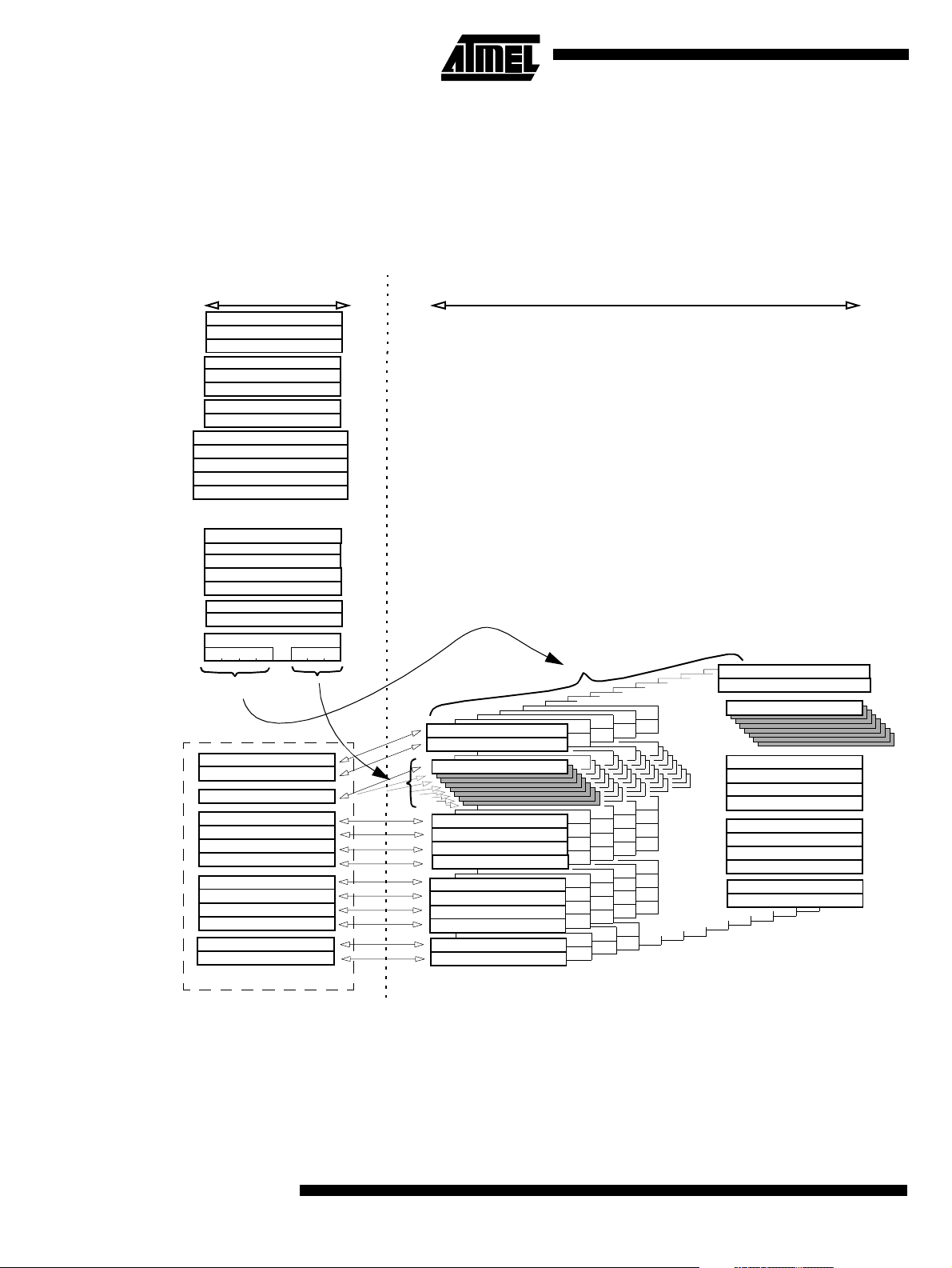
15.2 CAN Controller Mailbox and Registers Organization
Enable messageobject - 1
Enable messageobject - 2
Enable Interruptmessage object -1
Enable Interrupt message object - 2
Status Interrupt message object - 1
Status Interrupt message object - 2
CANTimer Low
Page message object
(message object number)(Data offset)
message objectStatus
message objectControl & DLC
Message Data
TimStmp High
TimStmp Low
The paginatio n allows man agement of the 321 regi sters inc luding 300(15x20) byt es of
mailboxvia34SFR’s.
All actions on the message objec t window SFRs apply to the corresponding m es sage
object registers pointed by the message object num ber find in the P age message object
register (CANPAGE) as illustrate in Fi gure 3 1.
Figure 31. CAN Controller memory organization
SFR’s on-chip CAN Controller registers
General Control
General Status
General Interrupt
Bit Timing -1
Bit Timing -2
Bit Timing -3
Enable Interrupt
Timer Control
CANTimer High
TimTTC High
TimTTC Low
TEC counter
REC counter
ID Tag - 1
ID Tag - 2
ID Tag - 3
ID Tag - 4
ID Mask- 1
ID Mask- 2
ID Mask- 3
ID Mask- 4
15 message objects
message object0 - Status
message o bject 0 - Control& DLC
Ch.0 - Message Data- byte 0
8bytes
Ch.0 - ID Tag - 1
Ch.0 - ID Tag - 2
Ch.0 - ID Tag - 3
Ch.0 - ID Tag - 4
Ch.0 - IDMask- 1
Ch.0 - IDMask- 2
Ch.0 - IDMask- 3
Ch.0-IDMask-4
Ch.0 TimStmp High
Ch.0 TimStmp Low
message object14 - Status
message object14 - Control& DLC
Ch.14 -Message Data - byte 0
Ch.14 - IDMask - 1
Ch.14 - IDMask - 2
Ch.14 - IDMask - 3
Ch.14 - IDMask - 4
Ch.14 TimStmp High
Ch.14 TimStmp Low
Ch.14 - ID Tag - 1
Ch.14 - ID Tag - 2
Ch.14 - ID Tag - 3
Ch.14 - ID Tag - 4
72
message object Window SFRs
T89C51CC01
Rev. D – 17-Dec-01
Page 73

T89C51CC01
15.2.1 Working on message
objects
15.3 CAN Controller management
The Page message object register (CANPAGE) is used to s elect one of t he 15 messa ge
objects. Then, message object Control (CANCONCH) and message object Status
(CANSTCH) are a va ilable for this selected mess age object number in the corresponding
SFRs. A single register (CANMSG) is used f or the message. The m ailbox pointer is
managed by the Page message object register with an auto-incrementation at the end of
each access. The range of this counter is 8.
Note that the maibo x is a pure RAM, dedicated to one message object, without overlap.
In m os t cases, it is not necessary to transfer the received mes sa ge into the standar d
memory. The message to be transmitted can be built directly in the maibox. Mos t calculations or tests can be executed in the mailbox area which provide quicker access.
In order to enable the CAN Controller correctly the following registers have to be
initialized:
• General Control (CANGCON),
• Bit Timing (CANBT 1,2&3),
• And for each page of 15 mes sage objects
– message obj ect Control (CANCONCH),
– message object Status (CANSTCH).
During operation, the CAN Enabl e message ob ject registers 1&2 (CANEN 1&2) gives a
fast overview of the message objects availability.
The CAN messages can be handled by interrupt or polling modes.
A message object can be configured as follows:
• Transmit message object,
• Receive message object,
• Receive buffer message object.
• Disable
This configuration is made in the CONCH field of the CA NCONCH register (see
Table 36).
When a message object is configured, the corresponding ENCH bit of CANEN 1&2 register is set.
Table 36. Configuration for CONCH1:2
CONCH 1 CONCH 2 Type of message object
00disable
01Transmitter
10Receiver
1 1 Receiver buffer
When a Transmitter or Receiver action of a message object is completed, the corresponding ENCH bit of t he CANEN 1&2 register is cleared. In order to re-enable the
message object, it is necessary to re-write the configuration in CANCONCH register.
Non-consecutive message objects can be used for all three ty pes of message object s
(Transmitter, Receiver and Receiver buf fer),
Rev. D – 17-Dec-01
73
Page 74

15.3.1 Buffer mode Any message object can be used to define one buffer, including non-consec utive mes-
sage objects, and with no limitat ion in number of message objects used up to 15.
Each message object of the buffer must be initialized CONCH2 = 1 and CONCH1 = 1;
Figure 32. Buffer mode
message object 14
message object 13
message object 12
message object 11
message object 10
message object 9
message object 8
message object 7
message object 6
message object 5
message object 4
message object 3
message object 2
message object 1
message object 0
Block buffer
buffer 7
buffer 6
buffer 5
buffer 4
buffer 3
buffer 2
buffer 1
buffer 0
The same acceptance filter must be defined for each message objects of the buffer.
When there is no ma sk on the identifier or the IDE, all messages are accepted.
A received frame will always be stored in the lowest free message object.
When the flag Rxok is set on one of the buffer message objects, this message object
can then be read by the application. This flag must then be cleared by the software a nd
the message object re-enabled in buffer reception in order to free the message object.
The OVRBUF flag in the CANGIT register is set when the buffer is full. This flag can
generate an interrupt.
The fram es following the b uffer-full interrupt will not stored a nd no status w ill b e overwritten in the CANSTCH registers involved in th e buffer until at least one of the buffer
message objects is re-enab led in reception.
This flag must be cleared by the software in order to acknowledge the interrupt.
15.4 IT CAN management The different interrupts are:
• Transmission interrupt,
• Reception interrupt,
• Interrupt on error (bit error, stuff error, crc error, form error, acknowledge error),
• Interrupt when Buffer receive is full,
• Interrupt on overrun of CAN Timer.
74
T89C51CC01
Rev. D – 17-Dec-01
Page 75

Figure 33. CAN Controller interrupt structure
T89C51CC01
RXOK i
CANSTCH.5
TXOK i
CANSTCH.6
BERR i
CANSTCH.4
SERR i
CANSTCH.3
CERR i
CANSTCH.2
FERR i
CANSTCH.1
AERR i
CANSTCH.0
OVRBUF
CANGIT.4
SERG
CANGIT.3
CERG
CANGIT.2
FERG
CANGIT.1
AERG
CANGIT.0
CANGIE.5
ENRX
CANGIE.4
ENTX
CANGIE.3
ENERCH
CANSIT1/2
SIT i
SIT i
CANIE1/2
EICH i
CANGIE.2
ENBUF
CANGIE.1
ENERG
i=0
i=14
IEN1.0
ECAN
CANIT
CANGIT.7
IEN1.2
ETIM
Rev. D – 17-Dec-01
OVRTIM
CANGIT.5
OVRIT
To enable a transmission interrupt:
• Enable General CAN IT in the interrupt system register,
• Enable interrupt by message ob ject, EICHi,
• Enable transmission interrupt, ENTX.
To enable a reception interrupt:
• Enable General CAN IT in the interrupt system register,
• Enable interrupt by message ob ject, EICHi,
• Enable reception interrupt, ENRX.
To enable an interrupt on mess age object error:
• Enable General CAN IT in the interrupt system register,
• Enable interrupt by message ob ject, EICHi,
• Enable interrupt on error, E NERCH.
75
Page 76

To enable an interrupt on general error:
• Enable General CAN IT in the interrupt system register,
• Enable interrupt on error, ENERG.
To enable an interrupt on Buffer-full condi tion:
• Enable General CAN IT in the interrupt system register,
• Enable interrupt on Buffer full, ENBUF.
To enable an interrupt when Timer o ve rrun s:
• Enable Overrun IT in the interrupt system register.
When an interrupt occurs, the corresponding message object bit is set in the SIT
register.
To acknowledge an interrupt, the corresponding CANSTCH bits (RXOK, TXOK,...) or
CANGIT bits (OVRTIM, OVRBUF,...), must be clea red by th e softw are ap plication.
When the CAN node is in transmission and detects a Form Error in its fram e, a bit Error
will also be ra ised. Consequently, two c ons ec ut ive interrupts can occur, both due to the
same error.
When a message object error oc cu rs and is set in CANSTCH regis ter, no general error
are set in CANGIE register.
15.5 Bit Timing and BaudRate
FCAN
CLOCK
Figure 34. sample and transmission point
Bit Timing
Prescaler BRP
Systemclock Tscl
TimeQuantum
PRS 3-bit length
PHS1 3-bit length
PHS2 3-bit length
SJW 2-bitlength
Samplepoint
Transmission point
The baud rate selection is ma de by Tbit calculation:
Tbit = Tsyns + Tprs + Tphs1 + Tphs2
1. Tsyns = Tscl = (BRP[5..0]+ 1) / Fcan = 1TQ.
2. Tprs = (1 to 8) * Tscl = (PR S[2..0]+ 1) * Tscl
3. Tphs1 = (1 to 8) * Tscl = (PHS1[2..0]+ 1) * Tscl
4. Tphs2 = (1 to 8) * Tscl = (PHS2[2..0]+ 1) * Tscl
5. Tsjw = (1 to 4) * Tscl = (SJW[1..0]+ 1) * Tscl
The total number of Tscl (Time Quanta) in a bit time must be comprised between 8 to
25.
76
T89C51CC01
Rev. D – 17-Dec-01
Page 77

Figure 35. General structure of a bit period
1/ Fcan
oscillator
T89C51CC01
systemclock
data
(1) Pha se error £ 0
(2) Pha se error Š 0
(3) Pha se error > 0
(4) Pha se error < 0
example of bit timing determination for CAN baudrate of 500kbit/s:
Fosc = 12 MHz in X1 mode => FCAN = 6MHz
Verify that the CANbaud rate you want is an integer division of FCAN clock.
FCAN/CANbaudrate = 6MHz/500kHz = 12
The time quanta TQ must be comprised between 8 and 25: TQ = 12 and BRP=0
Define the various timing parameters: Tbit = Tsyns + Tprs + Tphs1 + Tphs2 =
12TQ
Tsyns = 1TQ and Tsjw =1TQ => SJW=0
If we chose a sample point at 66.6% => Tphs2 = 4TQ => PHS2 = 3
Tbit=12=4+1+Tphs1 + Tprs, let us choose Tprs = 3 Tphs1 = 4
PHS1 = 3 and PRS=2
Tscl
Bit Rate Prescaler
one nominal bit
Tsyns( *)
(*) Synchronization Segment: SYNS
Tsyns = 1xTscl (fixed)
Tprs
Tbit calculation:
Tphs1 (1)
Tphs1 + Tsjw (3)
Tbit
Tbit Tsyns Tprs Tphs1 Tphs2++ +=
Tphs2 - Tsjw (4)
Sample Point
Tphs2 (2)
Transmission Point
Rev. D – 17-Dec-01
BRP=0soCANBT1 = 00h
SJW=0andPRS=2soCANBT2 = 04h
PHS2=3andPHS1=3soCANBT3 = 36h
77
Page 78

15.6 Fault Confinement With respect to fault confinement, a unit may be in one of the three following status:
• error active,
• error passive,
• bus off.
An error active unit takes part in bus communication and can send an active error frame
when the CAN macro detects an e rror.
An error passive unit cannot send an active error frame. It t akes part in bus c ommunication, but when an e rror is de tected, a passive erro r frame i s sent. Also, after a
transmission, an error passive unit will wait before initiating further trans mission.
A bus off unit is not allowed to have any influence on the bus.
For fault confinement, two error counters (TEC and REC) are implemented.
See CAN Specification f or details on Fault confinement.
Figure 36. Line error mode
TEC>127
or
REC>127
Error
Passive
Init.
Error
Active
TEC<127
and
REC<127
TEC>255
TEC: Transmit Error Counter
REC: Receive Error Counter
128 occurrences
of
11 consecutive
recessive
bit
Bus
Off
78
T89C51CC01
Rev. D – 17-Dec-01
Page 79

T89C51CC01
15.7 Acceptance filter Upon a reception hit (i.e., a good comparison between the ID+RTR+RB+IDE received
and an ID+RTR+RB+IDE specified while taking the comparison mask into account) the
ID+RTR+RB+IDE recei ved are written over th e ID TAG Registers.
ID => IDT0-29
RTR => RTRTAG
RB => RB0-1TAG
IDE => IDE in CANCONCH register
Figure 37. Acceptance filter block diagram
RxDC
Rx Shift Register (internal)
ID & RB RTR IDE
13/32
=
Write
Enable
13/32
13/32
ID TAG Registers (Ch i) & CanConch
ID & RB RTR
example:
To accept only ID = 318h in part A.
ID MSK = 111 1111 1111 b
ID TAG = 011 0001 1000 b
IDE
13/32
1
13/32
ID MSK Registers (Ch i)
ID & RB RTR IDE
Hit
(Ch i)
Rev. D – 17-Dec-01
79
Page 80

15.8 Data and Remote frame
message object in transmission
message object stay in
transmission
Description of the different steps for:
•Dataframe,
Node A Node B
H
C
R
T
N
E
R
0 1 x 0 0
0 0 x 1 0
K
K
V
L
O
O
P
X
X
R
T
R
D
u uu uu
c uc uu
A
T
A
F
R
A
M
• Remote frame, with au tomatic reply,
E
H
V
C
L
R
T
P
N
R
E
R
T
0 1 x 0 0
0 0 x 0 1
u uu uu
u cc uu
K
K
O
O
X
X
R
message object in reception
message object stay in reception
H
C
R
T
N
E
R
message object in transmission
message object in reception
by CAN controller by CAN controller
message object stay in
reception
1 1 x 0 0
0 1 x 1 0
0 0 x 0 1
K
K
V
L
O
O
P
X
X
R
T
R
R
E
M
u uu uu
c uu uc
u cc uu
O
T
E
F
R
A
M
E
E
M
A
R
F
)
e
A
t
T
a
i
A
d
e
D
m
m
i
(
H
C
R
T
N
E
R
R
1 1 1 0 0
0 1 0 0 0
0 0 0 1 0
K
K
V
L
O
O
P
X
X
T
R
u uu uu
u uu cc
c uc cu
message object in reception
message object in transmission
message object stay in transmission
• Remote frame.
message object in transmission
message object in reception
by CAN controller
message object in reception
by user
H
V
C
L
R
T
P
N
E
R
R
T
1 1 x 0 0
0 1 x 1 0
0 0 x 0 1
u uu uu
c uu uc
u cc uc
K
K
O
O
X
X
R
R
E
M
O
T
E
F
R
A
M
E
E
M
A
R
F
)
d
A
e
T
r
r
A
e
f
D
e
d
(
H
C
R
T
N
E
R
1 1 0 0 0
1 0 0 0 1
0 1 x 0 0
0 0 x 1 0
K
K
V
L
O
O
P
X
X
T
R
R
u uu uu
u cc uu
u uu uu
c uc uu
message object in reception
message object stay in reception
message object in transmission by user
message object stay in transmission
80
T89C51CC01
i
: modified by user
u
i
:modifiedbyCAN
c
Rev. D – 17-Dec-01
Page 81

T89C51CC01
15.9 Time Trigger Communication (TTC) and Message Stamping
The T89C51CC01 has a programmable 16-bit Timer (CANTIMH&CANTIML) for message stamp and TTC.
This CAN Timer starts after the CAN controller is enabled by the E NA bit in the CANGCON register.
Two modes in the timer are i mplemented:
• Time Trigger Communicat ion:
– Capture of this timer value in the CANTTCH & CANTTCL registers on Start
Of F r ame (SOF) or End Of Frame (EOF), depending on the SYNCTTC bit in
the CANGCON register, w hen the network is configured in TTC by the T TC
bit in the CANGCON register.
Note: In this mode, CAN only sends the frame once, even if an error occurs.
• Message Stamping
– Capture of this timer value in the CANSTMPH & CANS TM PL registers of the
message object which received or sent the frame.
– All mes s ages can be stamps.
– The s tamping of a received frame occurs when the RxOk flag is set.
– The stamping of a sent frame occurs when the T xOk f lag is set.
The CAN Timer works in a roll -over from FFFFh to 0000h which serves a s a time base.
When t he timer rol l-over from FFFFh to 0000h, an interrupt is generated if the ETIM bit
in the interrupt enable register IEN1 i s set.
Fcan
CLOCK
TXOK i
CANSTCH.4
RXOK i
CANSTCH.5
Figure 38. Block diagram of CAN Timer
÷ 6
CANTCON
CANTIMH & CANTIML
CANSTMPH & CANSTMPL
CANGCON.1
ENA
CANTTCH & CANTTCL
When 0xFFFF to 0x0000
CANGCON.5
TTC
OVRTIM
CANGIT.5
CANGCON.4
SYNCTTC
SOF on CAN frame
EOF on CAN frame
Rev. D – 17-Dec-01
81
Page 82

15.10CAN Autobaudand Listening mode
To activate the Autobaud feature, the AU TOBAUD bit in t he CANGCON register must
be set. In t his mode, the CAN controller i s only listening to the line without acknowledging the re ceived m essages. It c annot send any message. The error flags are updated.
The bit timing can be adjusted until no error oc c urs (good c onfiguration find).
In this mode, the error counters are frozen.
To go back to the standard mode, the AUTOBAUD bit must be cleared.
Figure 39. Autobaud Mode
TxDC’
AUTOBAUD
CANGCON.3
RxDC’
15.11 Routines Examples 1. Init of CAN macro
// Reset the CAN macro
CANGCON = 01h;
// Disable CAN interrupts
ECAN = 0;
ETIM = 0;
// Init the Mailbox
for num_page =0; num_page <15; num_page++
{
CANPAGE = num_channel << 4;
CANCONCH = 00h
CANSTCH = 00h;
CANIDT1 = 00h;
CANIDT2 = 00h;
CANIDT3 = 00h;
CANIDT4 = 00h;
CANIDM1 = 00h;
CANIDM2 = 00h;
CANIDM3 = 00h;
CANIDM4 = 00h;
for num_data =0; num_data <8; num_data++)
{
CANMSG = 00h;
}
}
// Configure the bit timing
CANBT1 = xxh
CANBT2 = xxh
CANBT3 = xxh
TxDC
RxDC
1
0
82
T89C51CC01
Rev. D – 17-Dec-01
Page 83

T89C51CC01
// Enable the CAN macro
CANGCON = 02h
2. Configure message object 3 in reception to receive only standard (11-bit identifier) message 100h
// Select the message object 3
CANPAGE = 30h
// Enable the interrupt on this message object
CANIE2 = 08h
// Clear the status and control register
CANSTCH = 00h
CANCONCH= 00h
// Init the acceptance filter to accept only message 100h in standard mode
CANIDT1 = 20h
CANIDT2 = 00h
CANIDT3 = 00h
CANIDT4 = 00h
CANIDM1 = FFh
CANIDM2 = FFh
CANIDM3 = FFh
CANIDM4 = FFh
// Enable channel in reception
CANCONCH = 88h // enable reception
Note: to enable the CAN interrupt in reception:
EA = 1
ECAN = 1
CANGIE = 20h
3. Send a message on the mes sage object 12
// Select the message object 12
CANPAGE = C0h
// Enable the interrupt on this message object
CANIE1 = 01h
// Clear the Status register
CANSTCH = 00h;
// load the identifier to send (ex: 555h)
CANIDT1 = AAh;
CANIDT2 = A0h;
// load data to send
CANMSG = 00h
CANMSG = 01h
CANMSG = 02h
CANMSG = 03h
CANMSG = 04h
CANMSG = 05h
CANMSG = 06h
CANMSG = 07h
// configure the control register
CANCONCH = 18h
4. Interrupt routine
// Save the current CANPAGE
Rev. D – 17-Dec-01
83
Page 84

// Find the first message object which generate an interrupt in CANSIT1 and
CANSIT2
// Select the corresponding message object
// Analyse the CANSTCH register to identify which kind of interrupt is
generated
// Manage the interrupt
// Clear the status register CANSTCH = 00h;
// if it is not a channel interrupt but a general interrupt
// Manage the general interrupt and clear CANGIT register
// restore the old CANPAGE
84
T89C51CC01
Rev. D – 17-Dec-01
Page 85

15.12 CAN SFR’s Table 37. CAN SFR’s with reset values
(1)
0/8
1/9 2/A 3/B 4/C 5/D 6/E 7/F
T89C51CC01
F8h
F0h
E8h
E0h
D8h
D0h
C8h
C0h
B8h
B0h
A8h
IPL1
xxxx x000CH0000 0000
B
0000 0000
IEN1
xxxx x000CL0000 0000
ACC
0000 0000
CCON
00xx xx00
PSW
0000 0000
T2CON
0000 0000
P4
xxxx xx11
IPL0
x000 0000
P3
1111 1111
IEN0
0000 0000
CMOD
00xx x000
FCON
0000 0000
T2MOD
xxxx xx00
CANGIE
0000 0000
SADEN
0000 0000
CANPAGE
0000 0000
SADDR
0000 0000
CCAP0H
0000 0000
ADCLK
xx00 x000
CCAP0L
0000 0000
CCAPM0
x000 0000
EECON
xxxx xx00
RCAP2L
0000 0000
CANIE1
xx00 0000
CANSIT1
0x00 0000
CANSTCH
xxxx xxxx
CANGSTA
0000 0000
CCAP1H
0000 0000
ADCON
0000 0000
CCAP1L
0000 0000
CCAPM1
x000 0000
RCAP2H
0000 0000
CANIE2
0000 0000
CANSIT2
0000 0000
CANCONCH
xxxx xxxx
CANGCON
0000 x000
CCAP2H
0000 0000
ADDL
xxxx xx00
CCAP2L
0000 0000
CCAPM2
x0000000
TL2
0000 0000
CANIDM1
xxxx xxxx
CANIDT1
xxxx xxxx
CANBT1
xxxx xxxx
CANTIML
0000 0000
CCAP3H
0000 0000
ADDH
0000 0000
CCAP3L
0000 0000
CCAPM3
x000 0000
TH2
0000 0000
CANIDM2
xxxx xxxx
CANIDT2
xxxx xxxx
CANBT2
xxxx xxxx
CANTIMH
0000 0000
CCAP4H
0000 0000
ADCF
0000 0000
CCAP4L
0000 0000
CCAPM4
x0000000
CANEN1
xx000000
CANIDM3
xxxx xxxx
CANIDT3
xxxx xxxx
CANBT3
xxxx xxxx
CANSTMPL
0000 0000
IPH1
xxxx x000
CANEN2
0000 0000
CANIDM4
xxxx xxxx
CANIDT4
xxxx xxxx
IPH0
x000 0000
CANSTMPH
0000 0000
FFh
F7h
EFh
E7h
DFh
D7h
CFh
C7h
BFh
B7h
AFh
A0h
98h
90h
88h
80h
P2
1111 1111
SCON
0000 0000
P1
1111 1111
TCON
0000 0000
P0
1111 1111SP0000 0111
(1)
0/8
CANTCON
0000 0000
SBUF
0000 0000
TMOD
0000 0000
1/9 2/A 3/B 4/C 5/D 6/E 7/F
AUXR1
0000 0000
TL0
0000 0000
DPL
0000 0000
CANMSG
xxxx xxxx
CANGIT
0x00 0000
TL1
0000 0000
DPH
0000 0000
CANTTCL
0000 0000
CANTEC
0000 0000
TH0
0000 0000
CANTTCH
0000 0000
CANREC
0000 0000
TH1
0000 0000
WDTRST
1111 1111
AUXR
0000 1000
WDTPRG
xxxx x000
CKCON
0000 0000
PCON
0000 0000
A7h
9Fh
97h
8Fh
87h
Rev. D – 17-Dec-01
85
Page 86

15.13 Registers Table 38. CANGCON Register
CANGCON (S:ABh)
CAN General Control Register
7654 3210
ABRQ OVRQ TTC SYNCTTC AUTOBAUD TEST ENA GRES
Bit
Number Bit Mnemonic Description
Abort request
Not an auto-resetable bit. A reset of the ENCH bit (message object control &
7ABRQ
6OVRQ
5TTC
4 SYNCTTC
DLC register) is done for each message object. The pending transmission
communications are immediately aborted but theon-going communicationwill
be terminated normally, setting the appropriate status flags, TXOK or RXOK.
Overload framerequest (initiator).
Auto-resetable bit.
Set to sendan overload frameafter the next received message.
Cleared by the hardwareatthebeginning of transmissionoftheoverload
frame.
Network in Timer Trigger communication
set to select node in TTC.
clear to disable TTC features.
Synchronization of TTC
When thisbit is set the TTC timeris caught on the lastbitof the End Of Frame.
When thisbit is cleartheTTCtimer is caught on the Start Of Frame.
This bitisonly used in the TTCmode.
3 AUTOBAUD
2TEST
1ENA/STB
0GRES
Reset Value: 0000 0x00b
AUTOBAUD
set to active listening mode.
Cleartodisablelistening mode
Te st mode. The test mode is intended for factorytestingandnotfor customer
use.
Enable/Standby CAN controller
When thisbit is set, it enables the CAN controllerandits input clock.
When thisbit is clear, the on-going communicationis terminatednormally and
theCANcontrollerstateofthemachineisfrozen(theENCHbitofeach
message object does not change).
In the standby mode, thetransmitter constantly provides a recessive level;the
receiver is not activated and the input clock is stopped in the CAN controller.
During the disablemode, the registers and themailbox remainaccessible.
Notethattwo clockperiods are needed to starttheCAN controller state of the
machine.
General reset (softwarereset).
Auto-resetable bit.This reset command is ‘ORed’withthehardware reset in
order to reset the controller. After a reset, the controller is disabled.
86
T89C51CC01
Rev. D – 17-Dec-01
Page 87

CANGSTA (S:AAh)
CAN General Status Register
T89C51CC01
Table 39. CANGSTA Register
76543210
- OV FG - T BSY RBSY ENFG BOFF ERRP
Bit
Number
7-
6OVFG
5-
4 TBSY
3 RBSY
2ENFG
1BOFF
Bit
Mnemonic Description
Reserved
The values read from this bit is indeterminate. Do not set thisbit.
Overload frame flag (1)
This status bit is setby thehardwareas longas theproducedoverloadframe is
sent.
This flag does not generate an interrupt
Reserved
The values read from this bit is indeterminate. Do not set thisbit.
Transmitter busy (1)
This status bit is set by the hardware as long as the CAN transmitter generates a
frame (remote, data, overload or error frame) or an ack field. This bit is also
active during an InterFrame Spacing if a frame must be sent.
This flag does not generate an interrupt.
Receiver busy (1)
This status bit is set by the hardware as long as the CAN receiver acquires or
monitors a frame.
This flag does not generate an interrupt.
Enable on-chip CAN controller flag (1)
Because an enable/disable command is not effective immediately, this status bit
gives the true state of a chosen mode.
This flag does not generate an interrupt.
Bus off mode (1)
seeFigure36
Rev. D – 17-Dec-01
0 ERRP
Error passive mode (1)
seeFigure36
Note: 1. These fields are Read Only.
Reset Value: x0x0 0000b
87
Page 88

CANGIT (S:9Bh)
CAN General Interrupt
Table 40. CANGIT Register
76543210
CANIT - OVRTIM OVRBUF SERG CERG FERG AERG
Bit
Number
7CANIT
6-
5OVRTIM
4OVRBUF
3 SERG
2CERG
Bit
Mnemonic Description
General interrupt flag (1)
This status bit is the image of all the CAN controller interrupts sent to the
interrupt controller.
Itcanbeusedinthecaseofthepollingmethod.
Reserved
The values read from this bit is indeterminate. Do not set thisbit.
Overrun CAN Timer
This status bit is set when the CAN timer switches 0xFFFF to 0x0000.
If the bit ETIM in theIE1registerisset,aninterruptis generated.
Clear this bit in order to reset the interrupt.
Overrun BUFFER
0 - no interrupt.
1 - IT turned on
This bit is set when the buffer is full.
Bit resetablebyuser.
seeFigure33.
Stuff error General
Detectionofmorethanfiveconsecutivebitswiththesamepolarity.
This flag can generate an interrupt. resetable by user.
CRC errorGeneral
The receiver performs a CRC check on each destuffed received message from
thestartofframeuptothedatafield.
If this checking does not matchwith the destuffedCRC field, a CRC error is set.
This flag can generate an interrupt. resetable by user.
88
T89C51CC01
Form error General
The form error results from one or more violations of the fixed formin the
following bit fields:
1FERG
0 AERG
CRC delimiter
acknowledgmentdelimiter
end_of_frame
This flag can generate an interrupt. resetable by user.
AcknowledgmenterrorGeneral
No detection of the dominant bit in the acknowledgeslot.
This flag can generate an interrupt. resetable by user.
Note: 1. These fields are Read Only.
Reset Value: 0x00 000 0b
Rev. D – 17-Dec-01
Page 89

CANTEC (S:9Ch Read Only)
CAN Transmit Error Counter
T89C51CC01
Table 41. CANTEC Register
76543210
TEC7 TEC6 TEC5 TEC4 TEC3 TEC2 TEC1 TEC0
CANREC (S:9Dh Read Only)
CAN Reception Error Counter
Bit
Number
7-0 TEC7:0
Bit
Mnemonic Description
TransmitError Counter
seeFigure36
Reset Value: 00h
Table 42. CANREC Register
76543210
REC7 REC6 REC5 REC4 REC3 REC2 REC1 REC0
Bit
Number
7-0 REC7:0
Bit
Mnemonic Description
Reception Error Counter
seeFigure36
Reset Value: 00h
Table 43. CANGIE Register
CANGIE (S:C1h)
CAN General Interrupt Enable
Rev. D – 17-Dec-01
76543210
- - ENRX ENTX ENERCH ENBUF ENERG -
Bit
Number
7-6 -
5 ENRX
4ENTX
3 ENERCH
Bit
Mnemonic Description
Reserved
The values read from thesebits are indeterminate. Do not setthese bits.
Enable receive interrupt
0-Disable
1-Enable
Enable transmit interrupt
0-Disable
1-Enable
Enable message object error interrupt
0-Disable
1-Enable
89
Page 90

Bit
Number
2 ENBUF
1 ENERG
Bit
Mnemonic Description
Enable BUF interrupt
0-Disable
1-Enable
Enable general error interrupt
0-Disable
1-Enable
CANEN1 (S:CEh Read Only)
CAN Enable message objec t
Registers 1
0-
Reserved
The value readfrom this bit is indeterminate.Donot set this bit.
Note: see Figure 33
Reset Value: xx00 000xb
Table 44. CANEN1 Register
76543210
- ENCH14 ENCH13 ENCH12 ENCH11 ENCH10 ENCH9 ENCH8
Bit
Number
7-
6-0 ENCH14:8
Bit
Mnemonic Description
Reserved
The values read from this bit is indeterminate. Do not set thisbit.
Enable message object
0 - messageobject is disabled => themessage objectis free foranewemission
or reception.
1 - message objectisenabled.
Thisbit isresetablebyre-writingthe CANCONCHof thecorrespondingmessage
object.
90
Reset Value: x000 000 0b
T89C51CC01
Rev. D – 17-Dec-01
Page 91

CANEN2 (S:CFh Read Only)
CAN Enable message objec t
Registers 2
T89C51CC01
Table 45. CANEN2 Register
76543210
ENCH7 ENCH6 ENCH5 ENCH4 ENCH3 ENCH2 ENCH1 ENCH0
CANSIT1 (S:BAh)
CAN Status Interrupt me ssage
object Registers 1
Bit
Number
7-0 ENCH7:0
Bit
Mnemonic Description
Enable message object
0 - messageobject is disabled => themessage objectis free foranewemission
or reception.
1 - message objectisenabled.
Thisbit isresetablebyre-writingthe CANCONCHof thecorrespondingmessage
object.
Reset Value: 0000 0000b
Table 46. CANSIT1 Register
76543210
- SIT14 SIT13 SIT12 SIT11 SIT10 SIT9 SIT8
Bit
Number
7-
Bit
Mnemonic Description
Reserved
The values read from this bit is indeterminate. Do not set thisbit.
Rev. D – 17-Dec-01
Status of interrupt by message object (1)
0 - no interrupt.
6-0 SIT14:8
1 - IT turned on. Resetwhen interrupt condition is cleared by user.
SIT14:8 = 0b 0000 1001 -> IT’s on message objects 11 & 8.
seeFigure33.
Note: 1. This field is Read Only
Reset Value: x000 000 0b
91
Page 92

CANSIT2 (S:BBh Read Only)
CAN Status Interrupt me ssage
object Registers 2
Table 47. CANSIT2 Register
76543210
SIT7 SIT6 SIT5 SIT4 SIT3 SIT2 SIT1 SIT0
CANIE1 (S:C2h)
CAN Enable Interrupt message
object Registers 1
Bit
Number
7-0 SIT7:0
Bit
Mnemonic Description
Status of interrupt by message object
0 - no interrupt.
1 - IT turned on. Resetwhen interrupt condition is cleared by user.
SIT7:0=0b00001001->IT’sonmessageobjects3&0.
seeFigure33.
Reset Value: 0000 0000b
Table 48. CANIE1 Register
76543210
- IECH14 IECH13 IECH12 IECH11 IECH10 IECH9 IECH8
Bit
Number
7-
6-0 IECH14:8
Bit
Mnemonic Description
Reserved
The values read from this bit is indeterminate. Do not set thisbit.
Enable interrupt by message object
0 - disable IT.
1 - enable IT.
IECH14:8=0b00001100->EnableIT’sofmessageobjects11&10.
seeFigure33.
92
Reset Value: x000 000 0b
T89C51CC01
Rev. D – 17-Dec-01
Page 93

CANIE2 (S:C3h)
CAN Enable Interrupt message
object Registers 2
T89C51CC01
Table 49. CANIE2 Register
76543210
IECH 7 IECH 6 IECH 5 IECH 4 IECH 3 IECH 2 IECH 1 IECH 0
CANBT1 (S:B4h)
CAN Bit Timing Registers 1
Bit
Number
7-0 IECH7:0
Bit
Mnemonic Description
Enable interrupt by message object
0 - disable IT.
1 - enable IT.
IECH7:0 = 0b 0000 1100- > Enable IT’s of message objects 3 & 2.
Reset Value: 0000 0000b
Table 50. CANBT1 Register
76543210
- BRP 5 BRP 4 BRP 3 BRP 2 BRP 1 BRP 0 -
Bit
Number
7-
Bit
Mnemonic Description
Reserved
The value readfrom this bit is indeterminate.Donot set this bit.
Baud rate prescaler
The period of the CAN controller systemclock Tscl is programmableand
determines the individual bit timing.
Rev. D – 17-Dec-01
6-1 BRP5:0
0-
Reserved
The value readfrom this bit is indeterminate.Donot set this bit.
Tscl=
BRP[5..0] + 1
Fcan
Note: The CAN controller bit timing registers must be accessedonly if the CAN controller is dis-
abled with the ENA bit of the CANGCON register set to 0.
See Figure 35.
No default value after reset.
93
Page 94

CANBT2 (S:B5h)
CAN Bit Timing Registers 2
Table 51. CANBT2 Register
76543210
- SJW 1 SJW 0 - PRS 2 PRS 1 PRS 0 -
Bit
Number
7-
6-5 SJW1:0
4-
3-1 PRS2:0
0-
Bit
Mnemonic Description
Reserved
The value readfrom this bit is indeterminate.Donot set this bit.
Re-synchronizationjumpwidth
T ocompensate for phase shifts between clock oscillators of different bus
controllers, the controller must re-synchronize on any relevant signal edge of the
current transmission.
The synchronization jump width defines the maximum number of clock cycles. A
bit period may be shortened or lengthened by a re-synchronization.
Tsjw= Tscl x (SJW [1..0]+1)
Reserved
The value readfrom this bit is indeterminate.Donot set this bit.
Programming timesegment
This part of the bit time is used to compensate for the physical delay times within
the network.It istwice thesum ofthesignal propagationtimeon the busline, the
input comparator delay and the output driver delay.
Tprs = Tscl x (PRS[2..0] + 1)
Reserved
The value readfrom this bit is indeterminate.Donot set this bit.
94
Note: The CAN controller bit timing registers must be accessedonly if the CAN controller is dis-
abled with the ENA bit of the CANGCON register set to 0.
See Figure 35.
No default value after reset.
T89C51CC01
Rev. D – 17-Dec-01
Page 95

CANBT3 (S:B6h)
CAN Bit Timing Registers 3
T89C51CC01
Table 52. CANBT3 Register
76543210
- PHS2 2 PHS2 1 PHS2 0 PHS1 2 PHS1 1 PHS1 0 SMP
Bit
Number
7-
6-4 PHS2 2:0
3-1 PHS1 2:0
0SMP
Bit
Mnemonic Description
Reserved
The value readfrom this bit is indeterminate.Donot set this bit.
Phase segment 2
This phase is used to compensate for phaseedge errors.This segmentcanbe
shortened by the re-synchronization jump width.
Tphs2=Tscl x (PHS2[2..0] + 1)
Phase segment 1
This phase is used to compensate for phaseedge errors.This segmentcanbe
lengthened by there-synchronization jumpwidth.
Tphs1 = Tscl x (PHS1[2..0] + 1)
Sample type
0 - once, at the samplepoint.
1 - three times, the threefold sampling of the bus is the sample point and twice
over a distance of a 1/2 period of the Tscl. The result corresponds to the majority
decisionof the three values.
Note: The CAN controller bit timing registers must be accessedonly if the CAN controller is dis-
abled with the ENA bit of the CANGCON register set to 0.
See Figure 35.
Rev. D – 17-Dec-01
No default value after reset.
95
Page 96

CANPAGE (S:B1h)
CAN message object Page
Register
Table 53. CANPAGE Register
76543210
CHNB 3 CHNB 2 CHNB 1 CHNB 0 AINC INDX2 INDX1 INDX0
CANCONCH (S:B3h)
CAN message object Control
and DLC Register
Bit
Number
7-4 CHNB3:0
3AINC
2-0 INDX2:0
Bit
Mnemonic Description
Selection of message object number
The available numbers are: 0 to 14 (see Figure 31).
Auto increment of the index (activelow)
0 - auto-increment of theindex (default value).
1 - non-auto-increment of the index.
Index
Byte location of the data field forthedefinedmessage object (see Figure 31).
Reset Value: 0000 0000b
Table 54. CANCONCH Register
76543210
CONCH 1 CONCH 0 RPLV IDE DLC 3 DLC 2 DLC 1 DLC 0
Bit
Number
Bit
Mnemonic Description
96
T89C51CC01
Configuration ofmessage object
CONCH1 CONCH0
0 0: disable
7-6
5RPLV
4IDE
CONCH1:
0 1: Launch transmission
1 0: Enable Reception
0
1 1: Enable Reception Buffer
NOTE:
The user mustre-writetheconfiguration to enablethe correspondingbitinthe
CANEN1:2 registers.
Reply valid
Used in the automaticreply mode afterreceivinga remoteframe
0 - reply not ready.
1 - reply ready & valid.
Identifier extension
0-CANstandardrev2.0A(ident=11bits).
1 - CAN standard rev 2.0 B (ident = 29 bits).
Rev. D – 17-Dec-01
Page 97

T89C51CC01
CANSTCH (S:B2h)
CAN message object Status
Register
Bit
Number
3-0 DLC3:0
Bit
Mnemonic Description
Data length code
Number of bytes in the data field of the message.
The rangeofDLCisfrom 0 up to 8.
This value is updated when a frame is received (data or remote frame).
If the expected DLC differs from the incoming DLC,a warning appearsinthe
CANSTCH register.
No default value after reset
Table 55. CANSTCH Register
76543210
DLCW TXOK RXOK BERR SERR CERR FERR AERR
Bit
Number
7DLCW
Bit
Mnemonic Description
Datalength code warning
The incoming messagedoes not have the DLC expected.Whatever the frame
type, the DLC field of the CANCONCH register is updated by the received DLC.
TransmitOK
6TXOK
5RXOK
4 BERR
3 SERR
2CERR
The communication enabled by transmission is completed.
Whenthecontrolleris ready tosend a frame, iftwoor more message objectsare
enabled as producers, the lowerindex message object (0 to 13) is suppliedfirst.
This flag can generate an interrupt.
Receive OK
The communication enabled by reception is completed.
In the caseoftwoormoremessage object reception hits,the lower index
messageobject (0 to 13) is updated first.
This flag can generate an interrupt.
Bit error (only in transmission)
The bit value monitoredis differentfrom the bit valuesent.
Exceptions:
the monitoredrecessivebit sent as a dominant bitduring the arbitration fieldand
the acknowledgeslotdetecting a dominant bit duringthesending of an error
frame.
This flag can generate an interrupt.
Stuff error
Detectionofmorethanfiveconsecutivebitswiththesamepolarity.
This flag can generate an interrupt.
CRC error
The receiver performs a CRC check on each destuffed received message from
thestartofframeuptothedatafield.
If this checking does not matchwith the destuffedCRC field, a CRC error is set.
This flag can generate an interrupt.
Rev. D – 17-Dec-01
97
Page 98

CANIDT1 for V2.0 part A
(S:BCh)
CAN Identifier Tag Registers 1
Bit
Number
1FERR
0 AERR
Bit
Mnemonic Description
Form error
The form error results from one or more violations of the fixed formin the
following bit fields:
CRC delimiter
acknowledgmentdelimiter
end_of_frame
This flag can generate an interrupt.
Acknowledgmenterror
No detection of the dominant bit in the acknowledgeslot.
This flag can generate an interrupt.
Note: See Figure 33.
No default value after reset.
Table 56. CANIDT1 Re gister for V2.0 part A
76543210
IDT 10 IDT 9 IDT 8 IDT 7 IDT 6 IDT 5 IDT 4 IDT 3
CANIDT2 for V2.0 part A
(S:BDh)
CAN Identifier Tag Registers 2
Bit
Number
7-0 IDT10:3
Bit
Mnemonic Description
IDentifier tag value
See Figure 37.
No default value after reset.
Table 57. CANIDT2 Re gister for V2.0 part A
76543210
IDT 2 IDT 1 IDT 0 - - - - -
Bit
Number
7-5 IDT2:0
4-0 -
Bit
Mnemonic Description
IDentifier tag value
See Figure 37.
Reserved
The values read from thesebits are indeterminate. Do not setthese bits.
No default value after reset.
98
T89C51CC01
Rev. D – 17-Dec-01
Page 99

CANIDT3 for V2.0 part A
(S:BEh)
CAN Identifier Tag Registers 3
T89C51CC01
Table 58. CANIDT3 Re gister for V2.0 part A
76543210
--------
CANIDT4 for V2.0 part A
(S:BFh)
CAN Identifier Tag Registers 4
Bit
Number
7-0 -
Bit
Mnemonic Description
Reserved
The values read from thesebits are indeterminate. Do not setthese bits.
No default value after reset.
76543210
- - - - - RTRTAG - RB0TAG
Bit
Number
7-3 -
2RTRTAG
1-
0RB0TAG
Bit
Mnemonic Description
Reserved
The values read from thesebits are indeterminate. Do not setthese bits.
Note: Remote transmission request tag value.
Reserved
The values read from thisbitare indeterminate.Do not setthese bit.
Note: Reserved bit 0 tag value.
CANIDT1 for V2.0 part B
(S:BCh)
CAN Identifier Tag Registers 1
Rev. D – 17-Dec-01
No default value after reset.
Table 59. CANIDT4 Re gister for V2.0 part A
76543210
IDT 28 IDT 27 IDT 26 IDT 25 IDT 2 4 IDT 23 IDT 22 IDT 21
Bit
Number
7-0 IDT28:21
Bit
Mnemonic Description
IDentifier tag value
See Figure 37.
No default value after reset.
99
Page 100

CANIDT2 for V2.0 part B
(S:BDh)
CAN Identifier Tag Registers 2
Table 60. CANIDT2 Re gister for V2.0 part B
76543210
IDT 20 IDT 19 IDT 18 IDT 17 IDT 1 6 IDT 15 IDT 14 IDT 13
CANIDT3 for V2.0 part B
(S:BEh)
CAN Identifier Tag Registers 3
Bit
Number
7-0 IDT20:13
Bit
Mnemonic Description
IDentifier tag value
See Figure 37.
No default value after reset.
Table 61. CANIDT3 Re gister for V2.0 part B
76543210
IDT 12 IDT 11 IDT 10 IDT 9 IDT 8 IDT 7 IDT 6 IDT 5
Bit
Number
7-0 IDT12:5
Bit
Mnemonic Description
IDentifier tag value
See Figure 37.
No default value after reset.
Table 62. CANIDT4 Re gister for V2.0 part B
CANIDT4 for V2.0 part B
(S:BFh)
CAN Identifier Tag Registers 4
100
T89C51CC01
76543210
IDT 4 IDT 3 IDT 2 IDT 1 IDT 0 RTRTAG RB1TAG RB0TAG
Bit
Number
7-3 IDT4:0
2RTRTAGRemote transmission request tag value
1RB1TAG
0RB0TAG
Bit
Mnemonic Description
IDentifier tag value
See Figure 37.
Note: Reserved bit 1 tag value.
Note: Reserved bit 0 tag value.
No default value after reset.
Rev. D – 17-Dec-01
 Loading...