

Page 1

1. Features
• 80C51 core architecture:
– 256 bytes of on-chip RAM
– 1 Kbytes of on-chip ERAM
– 32 Kbytes of on-chip Flash memory
Data Retention: 10 years at 85°C
Read/Write cycle: 10k
– 2 Kbytes of on-chip Flash for Bootloader
– 2 Kbytes of on-chip EEPROM
Read/Write cycle: 100k
– 14-sources 4-level interrupts
– Three 16-bit timers/counters
– Full duplex UART compatible 80C51
– Maximum crystal frequency 40 MHz. In X2 mode, 20 MHz (CPU core, 40 MHz)
– Five ports: 32 + 2 digital I/O lines
– Five-channel 16-bit PCA with:
PWM (8-bit)
High-speed output
Timer and edge capture
– Double Data Pointer
– 21-bit watchdog timer (7 programmable bits)
• A 10-bit r esolution analog to digitalconverter (ADC) with 8 m ultiplexed inputs
• On-chip emulation Logic (enhanced Hook system)
• Power saving modes:
– Idle mode
– Power down mode
• Power supply: 5V +/- 10% (or 3V** +/- 10%)
• Temperature range: Industrial (-40° to +85°C)
• Packages: TQFP44, PLCC44
Note:
* AtB RP = 1 sampling p oint will be fixed.
** Askfor availability
Enhance d 8-bit
MCU with A/D
Converter and
32 Kbytes
T89C51AC2
2. Description
The T89C51AC2 is a high performance FLASH version of the 80C51 single chip 8-bit
microcontrollers. It contains a 32Kbyte Flash memory block for program and data.
The 32K byte FLASH memory can be programmed either in parallel mod e or in serial
mode with the ISP capability or with software. The programming voltage is internally
generated from the standard V CC pin.
The T89C51AC2 retains all feat ures of the 80C52 with 256 bytes of internal RAM, a 7source 4-level interrupt controller and three timer/counters. In addition, the
T89C51AC2 has a 10 bit A/D converter, a 2Kbytes Boot Flash memory, 2 Kbyte
EEPROM for data, a Programm able Counter Array, an XRAM of 1024 bytes, a Hardware Watchdog Timer and a more versatile serial channel that facilitates
multiprocessor communication (EUART).The fully static design of the T89C51AC2
allows to reduc e system power consumption by bringing the clock frequency down to
any value, even DC, without loss of data.
The T89C51AC2 has 2 software-selectable modes of reduced activity and an 8 bit
clock prescaler for f urther reduction in power consumption. In the idle mode the CPU
is frozen while the pe ripherals and the interrupt system are still operating. In the
power-down mode the RAM is saved and all other functions are inoperative.
Rev. B – 19-Dec-01
1
Page 2
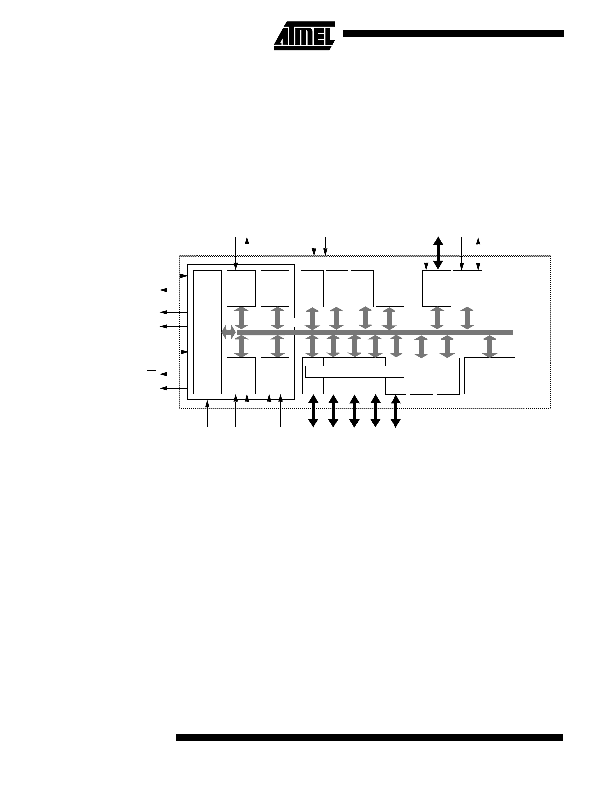
3. Block Diagram
The added features of the T89C51AC2 mak e it more powerful f or applications that need
A/D conversion, pulse width modulation, high spee d I/O and counting capabilities such
as industrial control, consumer goods, alarms, motor control, etc.
While remaining fully compatible with the 80C52 it offers a superset of this standard
microcontroller. In X2 mode a maximum external clock rate of 20 MHz reaches a 300 ns
cycle time.
PCA
RxD
TxD
Vss
Vcc
ECI
T2EX
T2
XTAL1
XTAL2
ALE
PSEN
EA
RD
WR
CPU
T0
C51
CORE
T1
RAM
256x8
INT
Ctrl
INT0
UART
Timer 0
Timer 1
RESET
Flash
Boot
32kx
loader
8
2kx8
IB-bus
Parallel I/O Ports & Ext. Bus
Port 0P0Port 1
INT1
(1): 8 analog Inputs / 8 Digital I/O
(2): 2-BitI/O Port
Port 2
P1(1)
EE
PROM
2kx8
P2
Port 3
ERAM
1kx8
Port 4
P3
PCA
Timer2
Emul
Watch
P4(2)
Dog
Unit
10 bit
ADC
2
T89C51AC2
Rev. B – 19-Dec-01
Page 3
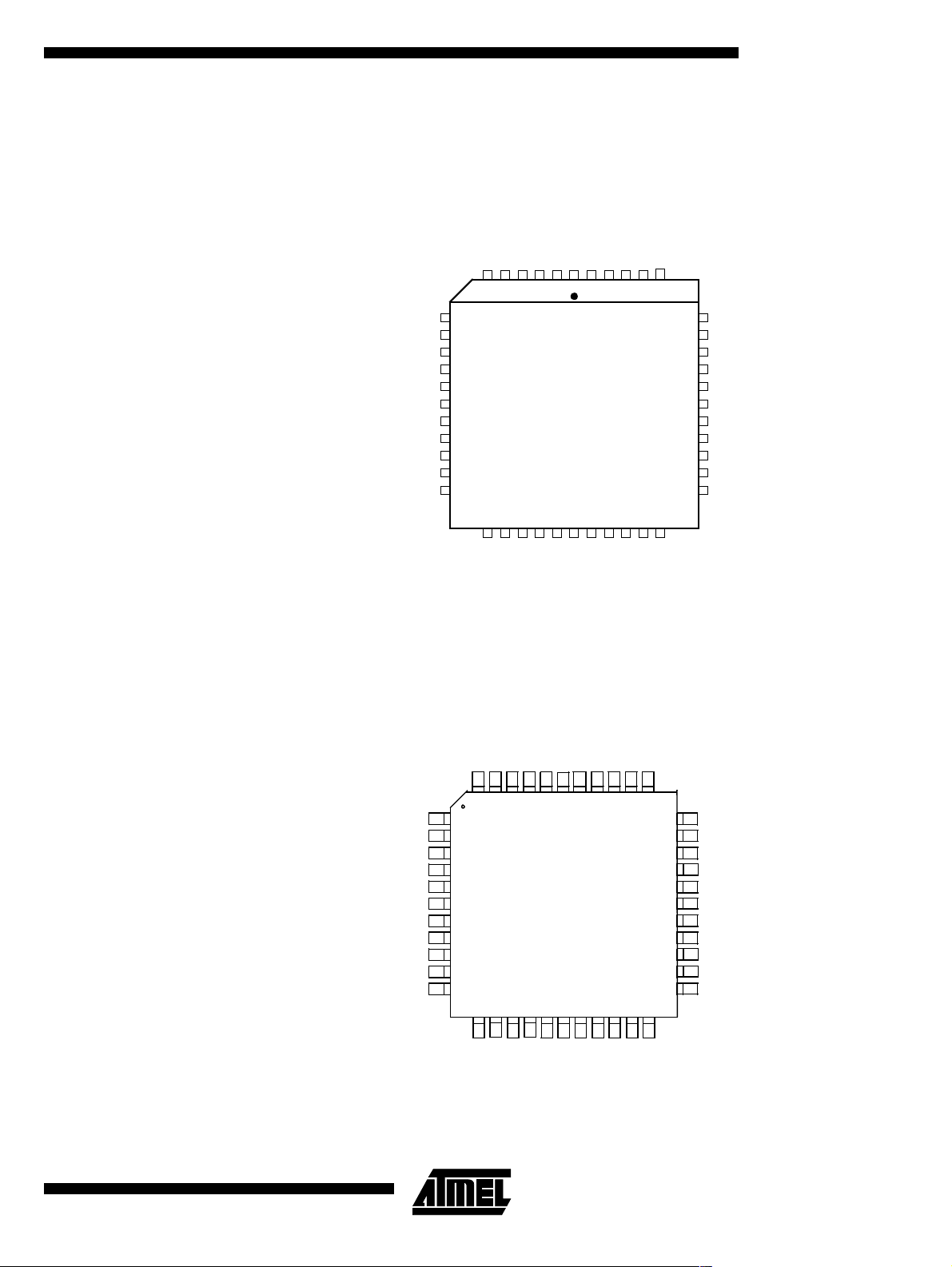
4. Pin Configuration
P1.4 / AN4 / CEX1
P1.5 / AN5 / CEX2
P1.6 / AN6 / CEX3
P1.7 / AN7 / CEX4
EA
P3.0/ RxD
P3.1 / TxD
P3.2 / INT0
P3.3 / INT1
P3.4 / T0
P3.5 / T1
7
8
9
10
11
12
13
14
15
16
17
P1.3 / AN3 / CEX0
P1.2 / A N2 / ECI
P1.1 / AN1 / T2EX
P1.0 / AN 0 / T2
65432
PLCC44
VAREF
VAGND
RESET
1
4443424140
T89C51AC2
VSS
VCC
XTAL1
XTAL2
39
ALE
38
PSEN
37
P0.7 / AD7
36
P0.6 / AD6
35
P0.5 / AD5
34
P0.4 / AD4
33
P0.3 / AD3
32
P0.2 / AD2
31
P0.1 / AD1
30
P0.0 / AD0
29
P2.0 / A8
P1.4 / AN4 / CEX1
P1.5 / AN5 / CEX2
P1.6 / AN6 / CEX3
P1.7 / AN7 / CEX4
EA
P3.0 / RxD
P3.1 / TxD
P3.2 / INT0
P3.3 / INT1
P3.4/ T0
P3.5/ T1
1819202122232425262728
P4.1
P4.0
P3.7/ RD
P3.6 / WR
P1.3 / AN3 / CEX0
P1.2 / AN2 / ECI
P1.1 / AN1 / T2EX
43 42 41 40 3944
1
2
3
4
5
6
7
8
9
10
11
P2.6/ A14
P2.7 / A15
P1.0/ AN0 /T2
VAREF
VAGND
38 37 36 35 34
TQFP44
P2.5/ A13
RESET
VSS
12 13 17161514 201918 21 22
P2.4/ A12
P2.1 / A9
P2.3/ A11
P2.2/ A10
VCC
XTAL1
XTAL2
33
ALE
32
PSEN
31
P0.7 / AD7
30
P0.6 / AD6
29
P0.5 / AD5
28
P0.4 /AD4
27
P0.3 /AD3
26
P0.2 /AD2
25
P0.1 /AD1
24
P0.0 /AD0
23
P2.0 / A8
Rev. B – 19-Dec-01
P4.1
P4.0
P3.7 / RD
P3.6 / WR
P2.7 / A15
P2.6 / A14
P2.5 / A13
P2.4 / A12
P2.1 / A9
P2.3 / A11
P2.2 / A10
3
Page 4

Table 1. Pin Description
Pin Name Type Description
VSS GND Circuit ground.
VCC Supply Voltage.
VAREF Reference Voltage for ADC
VAGND Reference Groundfor ADC
Port 0:
Is an 8-bit open drain bi-directional I/O port. Port 0 pins that have 1’s written to them float, and in this state can be used
P0.0:7 I/O
P1.0:7 I/O
as high-impedance inputs. Port 0 is also the multiplexedlow-orderaddress and databus during accessestoexternal
Program and Data Memory.Inthis applicationitusesstrong internal pull-ups whenemitting 1’s.
Port 0 also outputs thecodebytes duringprogram validation. External pull-ups are required during program
verification.
Port 1:
Is an 8-bit bi-directional I/O portwith internalpull-ups. Port 1 pins can be used fordigitalinput/output or as analog
inputs for the AnalogDigitalConverter( ADC). Port 1 pins that have1’s written to them are pulled high by the internal
pull-uptransistors andcanbe used as inputs inthis state.Asinputs,Port1pins thatare beingpulled lowexternally will
be the source of current (I
assigned to be used as analog inputs via the ADCCF register (in this case the internal pull-ups are disco nnected).
As a secondarydigitalfunction,port 1 containstheTimer 2 external trigger and clock input; the PCA external clock
input and the PCA module I/O.
P1.0 / AN0 / T2
Analoginput channel 0,
External clock input for Timer/counter2.
P1.1 / AN1 / T2EX
Analoginput channel 1,
Trigger inputfor Timer/counter2.
P1.2 / AN2 / ECI
Analoginput channel 2,
PCA external clock input.
P1.3 / AN3 / CEX0
Analoginput channel 3,
PCA module 0 Entry of input/PWM output.
P1.4 / AN4 / CEX1
Analoginput channel 4,
PCA module 1 Entry of input/PWM output.
P1.5 / AN5 / CEX2
Analoginput channel 5,
PCA module 2 Entry of input/PWM output.
P1.6 / AN6 / CEX3
Analoginput channel 6,
PCA module 3 Entry of input/PWM output.
P1.7 / AN7 / CEX4
Analoginput channel 7,
PCA module 4 Entry ot input/PWM output.
Port 1 receives the low-order address byte during EPROM programming and program verification.
It can drive CMOS inputs without external pull-ups.
, see section "Electrical Characteristic") because of the internal pull-ups. Port 1 pins are
IL
4
T89C51AC2
Rev. B – 19-Dec-01
Page 5

Pin Name Type Description
Port 2:
Is an 8-bit bi-directional I/O portwith internalpull-ups. Port 2 pins thathave1’s writtento them are pulled high by the
internal pull-ups and can be used as inputs in this state. As inputs, Port 2 pins that are being pulled low externally will
P2.0:7 I/O
P3.0:7 I/O
be a source of current (I
high-order address byte during accessestotheexternalProgram Memory and during accesses to external Data
Memory that uses 16-bit addresses (MOVX @DPTR). In this application, it uses strong internal pull-ups when emitting
1’s. During accesses to externalData Memory thatuse8bit addresses (MOVX@Ri), Port 2 transmits the contents of
theP2specialfunctionregister.
It also receives high-order addresses and control signals during program validation.
It can drive CMOS inputs without external pull-ups.
Port 3:
Is an 8-bit bi-directional I/O portwith internalpull-ups. Port 3 pins thathave1’s writtento them are pulled high by the
internal pull-up transistors and can be used as inputs in this state. As inputs, Port 3 pins that are being pulled low
externally will be a source of current (I
The outputlatch correspondingtoa secondary functionmustbeprogrammedtoone for that function to operate
(exceptforTxD and WR
P3.0 / RxD:
Receiver data input (asynchronous) or data input/output (synchronous) of the serial interface
P3.1 / TxD:
Transmitter data output(asynchronous)or clock output (synchronous) of the serialinterface
P3.2 / INT0
External interrupt 0 input / timer 0 gate control input
P3.3 / INT1
External interrupt 1 input / timer 1 gate control input
P3.4 / T0:
Timer0 counter input
P3.5 / T1:
Timer1 counter input
P3.6 / WR
External Data Memorywrite strobe; latches the databytefrom port 0 into the external data memory
P3.7 / RD
External Data Memory read strobe; Enables the external data memory.
It can drive CMOS inputs without external pull-ups.
:
:
:
:
, see section "Electrical Characteristic") because of the internal pull-ups. Port 2 emits the
IL
, see section"Electrical Characteristic") because of the internalpull-ups.
IL
). The secondary functions are assigned to the pins of port 3 as follows:
T89C51AC2
P4.0:1 I/O
Rev. B – 19-Dec-01
Port 4:
Is an 2-bit bi-directional I/O portwith internalpull-ups. Port 4 pins thathave1’s writtento them are pulled high by the
internal pull-ups and can be used as inputs in this state. As inputs, Port 4 pins that are being pulled low externally will
be a source of current (IIL,on thedatasheet)because of the internalpull-uptransistor.
P4.0
P4.1:
It can drive CMOS inputs without external pull-ups.
5
Page 6

Pin Name Type Description
Reset:
RESET I/O
ALE O
PSEN O
EA I
XTAL1 I
A high level on this pin during two machine cycles while the oscillator is running resets the device. An internal pulldown resistor to VSS permits power-on resetusing onlyan external capacitortoVCC.
ALE:
An Address Latch Enable output for latching the low byte of the address during accesses to the external memory. The
ALE is activated every1/6 oscillatorperiods (1/3 in X2 mode) except during an external datamemory access.When
instructions areexecuted from an internal FLASH (EA
PSEN
:
The Program Store Enableoutput is a controlsignal that enablesthe external program memoryofthe bus during
external fetch operations.Itisactivated twice each machine cycle during fetches fromthe external programmemory.
However,whenexecutingfrom of the externalprogram memory two activationsofPSENareskipped during each
access to the external Data memory. The PSEN is not activated for internal fetches.
EA
:
When External Access is held at the high level, instructions are fetched from the internal FLASH when the program
counterislessthen 8000H. When held at thelowlevel,T89C51AC2fetches allinstructions from theexternal program
memory
.
XTAL1:
Input of theinvertingoscillatoramplifier and input of theinternal clockgenerator circuits.
To drivethedevice fromanexternalclock source,XTAL1should be driven, while XTAL2isleft unconnected.To
operateabove a frequency of 16 MHz, a duty cycleof50%should be maintained.
= 1), ALE generation can be disabled by the software.
XTAL2 O
XTAL2:
Output from the inverting oscillator amplifier.
4.1 I/O Configurations Each Port SFR operates via type-D latches, as illustrated in Figure 1 for Ports 3 and 4. A
CPU "wri te to latch" signal initiates transfer of internal bus data into the type-D latch. A
CPU "read latch" signal tr ans f ers the latched Q output onto the internal bus. Similarly, a
"read pin" signal transfers the logical level of the Port pin. Some Port data instructio ns
activate the "read latch" signal while others activate the "read pin" signal. Latch instructions are referred to as Read-Mo dify-W rite instru ctions . Each I/O line may be
independently programm ed as input or output.
4.2 Port 1, Port 3 and Port 4
Figure 1 shows the structure of Port s 1 and 3, which ha ve internal pull-ups. An external
source can pull the pin low. Each Port pin can be configured either for general purpose
I/O or for its alternate input output func tion.
To use a pin for general purpose output, set or clear the corresponding bit in the Px register (x=1,3 or 4). To use a pin for general purpose input, set the bit in the Px regist er.
This turns off the output FET drive.
To configure a pi n for its alternate function, set the bit in the Px regist er. When the latch
is set, the "alternate output function" signal controls the output level (see Figure 1). The
operation of Port s 1, 3 and 4 is discussed further in "quasi-Bidirectional Port Operation"
paragraph.
6
T89C51AC2
Rev. B – 19-Dec-01
Page 7
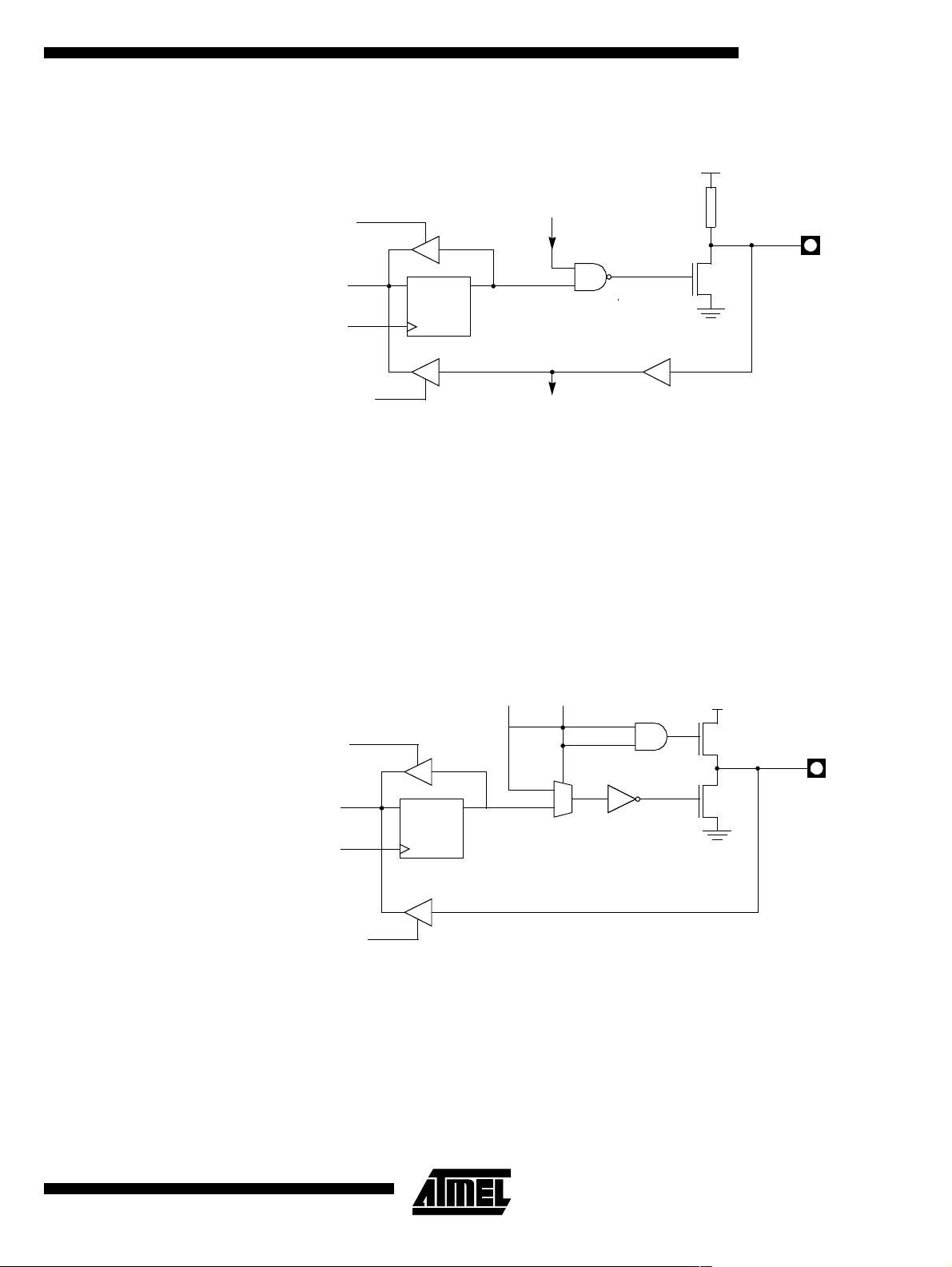
Figure 1. Port 1, Port 3 and Port 4 Structure
T89C51AC2
VCC
READ
LATCH
ALTERNATE
OUTPUT
FUNCTION
INTERNAL
PULL-UP (1)
P1.x
P3.x
INTERNAL
BUS
WRITE
TO
LATCH
READ
PIN
D
CL
P3.X
P4.X
LATCH
QP1.X
ALTERNATE
INPUT
FUNCTION
P4.x
Note: The internal pull-up can be disabled on P1 when analog function is selected.
4.3 Port 0 and Port2 P ort s 0 and 2 are used for general-purpose I/O or as the external address/data bus. Port
0, shown in Figure 3, differs from t he other Ports in not having internal pull-ups. Figure 3
shows the structure of Port 2. An external source can pul l a Port 2 pin low.
To use a pin for general-purpose output, set or c lear the corresponding bit in t he Px register ( x =0 or 2). To us e a pin for general purpose input, set the bit in the Px regist er to
turn off the output driver FET.
Figure 2. Port 0 Structure
READ
LATCH
ADDRESS LOW/
DATA
CONTROL
VDD
(2)
P0.x (1)
INTERNAL
BUS
WRITE
TO
LATCH
READ
PIN
D
P0.X
LATCH
Q
1
0
Notes: 1. Port 0 is precluded from use as general purpose I/O Ports when used as
address/data bus drivers.
2. Port 0 internalstrong pull-upsassist the logic-one output for memory bus cycles only.
Except for these bus cycles, the pull-up FET is off, Port 0 outputs are open-drain.
Rev. B – 19-Dec-01
7
Page 8
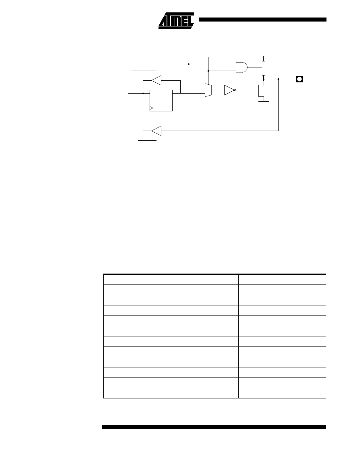
Figure 3. Port 2 Structure
READ
LATCH
INTERNAL
BUS
WRITE
TO
LATCH
READ
PIN
D
P2.X
LATCH
ADDRESS HIGH/
Q
CONTROL
1
0
Notes: 1. Port 2 is precluded from use as general purpose I/O Por ts when as address/data bus
drivers.
2. Port 2 internal strong pull-ups FET (P1 in FiGURE) assist the logic-one output for
memory bus cycle.
VDD
INTERNAL
PULL-UP (2)
P2.x (1)
When Port 0 and Port 2 are used for an ext ernal memo ry cycle, an internal control signal
switches the output-driver input from t he latch output to the internal address/data line.
4.4 Read-Modify-Write Instructions
Some inst ructions read the latch da ta rather than the pin data. The latch ba se d instructions read the data, modify th e data and t hen rewrite the latch. These are called "ReadModify-Write" instructions. Below is a complete list of these s pecial instructions (see
Table 2). When the destination operand is a Port o r a Port bit, thes e ins tructions read
the latch rather than the pin:
Table 2. Read-Modify-Write Instructions
Instruction Description Example
ANL logical AND ANL P1, A
ORL logical OR ORL P2, A
XRL logical EX-OR XRL P3, A
JBC jump if bit = 1 and clear bit JBC P1.1, LABEL
CPL complement bit CPL P3.0
INC increment INC P2
DEC decrement DEC P2
DJNZ decrement and jump if not zero DJNZ P3, LABEL
MOV Px.y, C move carrybitto bit y of Port x MOV P1.5,C
CLR Px.y clearbit y of Port x CLR P2.4
SET Px.y set bit y of Port x SET P3.3
8
T89C51AC2
Rev. B – 19-Dec-01
Page 9
T89C51AC2
It is not obvious the last three instructions in this list are Read-Modify-Write inst ructions.
These instructions read the port (all 8 bits), modify the specifically addressed bit and
write the new byte back to the latch. These Re ad-Modify-Write instructions are directed
to the latch rather than the pin in order to avoid possible misinterpretation of voltage
(and therefore, logic) levels at the pin. For example, a Port bit used to dri ve the base of
an external bipolar transistor can not rise above the transistor’s base-emitter junction
voltage (a value lower than VIL). With a logic one written to the bit, attempt s by the CPU
to read the Port at the pin are misinterpreted as logic zero. A read of the latch rather
than the pins returns the correct logic-on e val ue.
4.5 Quasi-Bidirectional Port Operation
Port 1, Port 2, Port 3 and Port 4 have fixed internal pull-ups and are referred to as
"quasi-bidirectional" Ports. When configured as an input, the pin im pedance appears as
logic one and sources current in response to an external logic zero condition. Port 0 is a
"true bidirectional" pin. The pins float when configured as inpu t. Resets write logic one to
all Port latches. If logical zero is subs equently written to a Port latch, it can be return ed
to input conditions by a logica l o ne written to the latch.
Note: Port latch values change near the end of Read-Modify-Write i nstruction cycles. O utput
buffers (and therefore t he pin state) update early in the instruction after Read-ModifyWrite instructioncycle.
Logical zero-to-one transitions in Port 1, Port 2, Port 3 and Port 4 use an additional pullup (p1) to aid this logic transition (see Figure 4. ). This increases switch speed. This
extra pull-up sources 100 times normal inte rnal c ircuit current during 2 oscillato r clock
periods. The internal pull-ups are field-effect t ransistors rather than linear resistors. Pullups consist of three p-channel FET (pFET) devices. A pFET is on when the gate senses
logical zero and off when the gate senses logical one. pFET #1 is turned on for two
oscillator periods immediately after a z ero-to-one transition in the Port latch. A logical
one at the Port pin turns on pFET #3 (a weak pull-up) through the inverter. This inverter
and pFET pair form a latch to drive logical one. pFET #2 is a very weak pull-up switched
on whenever the a ssociated nFET is switched off. This is traditional CMOS switch convention. Current strengths are 1/10 that of pFET #3.
Figure 4. Internal Pull-Up Configurations
2 Osc. PERIODS
VCCVCCVCC
Rev. B – 19-Dec-01
p1(1)
OUTPUT DATA
INPUT DATA
READ PIN
Note: Port 2 p1 assists the logic-one output for memory bus cycles.
p2
n
p3
P1.x
P2.x
P3.x
P4.x
9
Page 10

5. SFR Mapping The Special Function Registers (SFRs) of the T89C51AC2 fall into the following
categories:
Table 3. C51CoreSFRs
MnemonicAddName 76543210
ACC E0h Accumulator
BF0hBRegister
PSW D0h Program Status Word CY AC F0 RS1 RS0 OV F1 P
SP 81h Stack Pointer
Data Pointer Low
DPL 82h
DPH 83h
MnemonicAddName 76543210
P0 80h Port 0
P1 90h Port 1
byte
LSB of DPTR
Data Pointer High
byte
MSB of DPTR
Table 4. I/O Port SFRs
P2 A0h Port 2
P3 B0h Port 3
P4 C0h Port 4 (x2)
------
Table 5. TimersSFRs
MnemonicAddName 76543210
TH0 8Ch
TL0 8Ah
TH1 8Dh
TL1 8Bh
TH2 CDh
TL2 CCh
TCON 88h
Timer/Counter0High
byte
Timer/Counter 0 Low
byte
Timer/Counter1High
byte
Timer/Counter 1 Low
byte
Timer/Counter2High
byte
Timer/Counter 2 Low
byte
Timer/Counter 0 and
1 control
TF1 TR1 TF0 TR0 IE1 IT1 IE0 IT0
TMOD 89h
10
T89C51AC2
Timer/Counter 0 and
1 Modes
GATE1 C/T1# M11 M01 GATE0 C/T0# M10 M00
Rev. B – 19-Dec-01
Page 11

T89C51AC2
MnemonicAddName 76543210
T2CON C8h
T2MOD C9h
RCAP2H CBh
RCAP2L CAh
WDTRST A6h
WDTPRG A7h
Timer/Counter 2
control
Timer/Counter 2
Mode
Timer/Counter 2
Reload/Capture High
byte
Timer/Counter 2
Reload/Capture Low
byte
WatchDog Timer
Reset
WatchDog Timer
Program
TF2 EXF2 RCLK TCLK EXEN2 TR2 C/T2# CP/RL2#
------T2OEDCEN
-----S2S1S0
Table 6. Serial I/O Port SFRs
MnemonicAddName 76543210
SCON 98h Serial Control FE/SM0 SM1 SM2 REN TB8 RB8 TI RI
SBUF 99h Serial Data Buffer
SADEN B9h SlaveAddress Mask
SADDR A9h Slave Address
Table 7. PCA SFRs
MnemonicAddName 76543210
CCON D8h
CMOD D9h
CL E9h
CH F9h
CCAPM0
CCAPM1
CCAPM2
CCAPM3
CCAPM4
DAh
DBh
DCh
DDh
DEh
PCA Timer/Counter
Control
PCA Timer/Counter
Mode
PCA Timer/Counter
Low byte
PCA Timer/Counter
Highbyte
PCA Timer/Counter
Mode 0
PCA Timer/Counter
Mode 1
PCA Timer/Counter
Mode 2
PCA Timer/Counter
Mode 3
PCA Timer/Counter
Mode 4
CF CR - CCF4 CCF3 CCF2 CCF1 CCF0
CIDL WDTE - - - CPS1 CPS0 ECF
ECOM0
ECOM1
-
ECOM2
ECOM3
ECOM4
CAPP0
CAPP1
CAPP2
CAPP3
CAPP4
CAPN0
CAPN1
CAPN2
CAPN3
CAPN4
MAT0
MAT1
MAT2
MAT3
MAT4
TOG0
TOG1
TOG2
TOG3
TOG4
PWM0
PWM1
PWM2
PWM3
PWM4
ECCF0
ECCF1
ECCF2
ECCF3
ECCF4
Rev. B – 19-Dec-01
11
Page 12

MnemonicAddName 76543210
PCA Compare
Capture Module0 H
CCAP0H
CCAP1H
CCAP2H
CCAP3H
CCAP4H
CCAP0L
CCAP1L
CCAP2L
CCAP3L
CCAP4L
PCA Compare
FAh
Capture Module1 H
FBh
PCA Compare
FCh
Capture Module2 H
FDh
PCA Compare
FEh
Capture Module3 H
PCA Compare
Capture Module4 H
PCA Compare
Capture Module0 L
PCA Compare
EAh
Capture Module1 L
EBh
PCA Compare
ECh
Capture Module2 L
EDh
PCA Compare
EEh
Capture Module3 L
PCA Compare
Capture Module4 L
CCAP0H7
CCAP1H7
CCAP2H7
CCAP3H7
CCAP4H7
CCAP0L7
CCAP1L7
CCAP2L7
CCAP3L7
CCAP4L7
CCAP0H6
CCAP1H6
CCAP2H6
CCAP3H6
CCAP4H6
CCAP0L6
CCAP1L6
CCAP2L6
CCAP3L6
CCAP4L6
CCAP0H5
CCAP1H5
CCAP2H5
CCAP3H5
CCAP4H5
CCAP0L5
CCAP1L5
CCAP2L5
CCAP3L5
CCAP4L5
CCAP0H4
CCAP1H4
CCAP2H4
CCAP3H4
CCAP4H4
CCAP0L4
CCAP1L4
CCAP2L4
CCAP3L4
CCAP4L4
CCAP0H3
CCAP1H3
CCAP2H3
CCAP3H3
CCAP4H3
CCAP0L3
CCAP1L3
CCAP2L3
CCAP3L3
CCAP4L3
CCAP0H2
CCAP1H2
CCAP2H2
CCAP3H2
CCAP4H2
CCAP0L2
CCAP1L2
CCAP2L2
CCAP3L2
CCAP4L2
CCAP0H1
CCAP1H1
CCAP2H1
CCAP3H1
CCAP4H1
CCAP0L1
CCAP1L1
CCAP2L1
CCAP3L1
CCAP4L1
CCAP0H0
CCAP1H0
CCAP2H0
CCAP3H0
CCAP4H0
CCAP0L0
CCAP1L0
CCAP2L0
CCAP3L0
CCAP4L0
Table 8. Interrupt SFRs
MnemonicAddName 76543210
IEN0 A8h
IEN1 E8h
IPL0 B8h
IPH0 B7h
IPL1 F8h
IPH1 F7h
Interrupt Enable
Control 0
Interrupt Enable
Control 1
Interrupt Priority
Control Low 0
Interrupt Priority
Control High 0
Interrupt Priority
Control Low 1
Interrupt Priority
Control High1
EA EC ET2 ES ET1 EX1 ET0 EX0
------EADC-
- PPC PT2 PS PT1 PX1 PT0 PX0
- PPCH PT2H PSH PT1H PX1H PT0H PX0H
------PADCL-
------PADCH-
Table 9. ADC SFRs
MnemonicAddName 76543210
ADCON F3h ADC Control - PSIDLE ADEN ADEOC ADSST SCH2 SCH1 SCH0
ADCF F6h ADC Co nf iguration CH7 CH6 CH5 CH4 CH3 CH2 CH1 CH0
ADCLK F2h ADC Clock - - - PRS4 PRS3 PRS2 PRS1 PRS0
ADDH F5h ADC Data High byte ADAT9 ADAT8 ADAT7 ADAT6 ADAT5 ADAT4 ADAT3 ADAT2
ADDLF4hADCDataLowbyte------ADAT1ADAT0
12
T89C51AC2
Rev. B – 19-Dec-01
Page 13

T89C51AC2
Table 10. Other SFRs
MnemonicAddName 76543210
PCON 87h PowerControl SMOD1 SMOD0 - POF GF1 GF0 PD IDL
AUXR 8Eh Auxiliary Register 0 - - M0 - XRS1 XRS2 EXTRAM A0
AUXR1 A2h Auxiliary Register 1 - - ENBOOT - GF3 0 - DPS
CKCON 8Fh Clock Control - WDX2 PCAX2 SIX2 T2X2 T1X2 T0X2 X2
FCON D1h FLASH Control FPL3 FPL2 FPL1 FPL0 FPS FMOD1 FMOD0 FBUSY
EECON D2h EEPROM Contol EEPL3 EEPL2 EEPL1 EEPL0 - - EEE EEBUSY
Rev. B – 19-Dec-01
13
Page 14

0/8
Table 11. SFR’s mapping
(1)
1/9 2/A 3/B 4/C 5/D 6/E 7/F
F8h
F0h
E8h
E0h
D8h
D0h
C8h
C0h
B8h
B0h
A8h
IPL1
xxxx x000
B
0000 0000
IEN1
xxxx x000
ACC
0000 0000
CCON
0000 0000
PSW
0000 0000
T2CON
0000 0000
P4
xxxx xx11
IPL0
x000 0000
P3
1111 1111
IEN0
0000 0000
CH
0000 0000
CL
0000 0000
CMOD
00xx x000
FCON
0000 0000
T2MOD
xxxx xx00
SADEN
0000 0000
SADDR
0000 0000
CCAP0H
0000 0000
ADCLK
xxx0 0000
CCAP0L
0000 0000
CCAPM0
x000 0000
EECON
xxxx xx00
RCAP2L
0000 0000
CCAP1H
0000 0000
ADCON
x000 0000
CCAP1L
0000 0000
CCAPM1
x000 0000
RCAP2H
0000 0000
CCAP2H
0000 0000
ADDL
0000 0000
CCAP2L
0000 0000
CCAPM2
x000 0000
TL2
0000 0000
CCAP3H
0000 0000
ADDH
0000 0000
CCAP3L
0000 0000
CCAPM3
x0000000
TH2
0000 0000
CCAP4H
0000 0000
ADCF
0000 0000
CCAP4L
0000 0000
CCAPM4
x0000000
IPH1
xxxx x000
IPH0
x000 0000
FFh
F7h
EFh
E7h
DF
h
D7h
CF
h
C7h
BFh
B7h
AFh
A0h
98h
90h
88h
80h
P2
1111 1111
SCON
0000 0000
P1
1111 1111
TCON
0000 0000
P0
1111 1111
(1)
0/8
AUXR1
xxxx 00x0
SBUF
0000 0000
TMOD
0000 0000
SP
0000 0111
1/9 2/A 3/B 4/C 5/D 6/E 7/F
TL0
0000 0000
DPL
0000 0000
TL1
0000 0000
DPH
0000 0000
TH0
0000 0000
TH1
0000 0000
WDTRST
1111 1111
AUXR
x00x 1100
Reserved
Notes: 1. These registers are bit-addressable.
Sixteen addresses in the SFR space are both byte-addressable and bit-addressable.
The bit-addressable SFR’s are those whose address ends in 0 and 8. The bit
addresses, in this area, are 0x80 through to 0xFF.
WDTPRG
xxxx x000
CKCON
0000 0000
PCON
00x1 0000
A7h
9Fh
97h
8Fh
87h
14
T89C51AC2
Rev. B – 19-Dec-01
Page 15

T89C51AC2
6. Clock The T 89C51AC2 core needs only 6 clock periods per machine cycle. This feature,
called”X2”, provides the following advantages:
• Divides frequency crystals by 2 (che aper cry stals) while keeping the same CPU
power.
• Saves power consum ption while keeping the same CPU power (oscillator power
saving).
• Saves power consum ption by dividing dynamic operating frequency by 2 in
operating and idle modes.
• Increases CPU power by 2 while keeping the same crystal frequency.
In order to keep the original C51 compatibility, a divider-by-2 is inserted between the
XTAL1 signal and the main clock i nput of the core (phase generat or). This divider may
be disabled by the software.
An extra feature is available to start after Reset in the X2 mode. This feature can be
enabled by a bit X 2B in the Hardware Security Byte. This bit is des c ribed in the section
"In-System Programming".
6.1 Description The X2 bit in the CKCON register (see Table 12) allows switching from 12 clock cycles
per instruction to 6 clock cycles and vice versa. At reset, the standard speed is activat ed
(STD mode).
Setting this bit activates th e X2 featur e (X2 mod e) for the CPU Clock only (see Figure
5.).
The Timers 0, 1 and 2, Uart, P CA, or watchdog switch in X2 mode only if the corresponding bit is cleared in the C KCON register.
The clock for the whole circ uit and peripheral is first divided by two before being used by
the CPU core and peripherals. This allows any cyclic ratio to be accepted on the XTAL1
input. In X2 mode, as this divider is bypassed, the signals on XTAL1 must have a cyclic
ratio between 40 t o 60%. Figur e 5. shows the cloc k generation block diagram. The X2
bit is validated on the XTAL1÷2 rising edge to av oid glitches when switching from the X2
to the STD mode. Figure 6 shows the mo de switching waveforms.
Rev. B – 19-Dec-01
15
Page 16
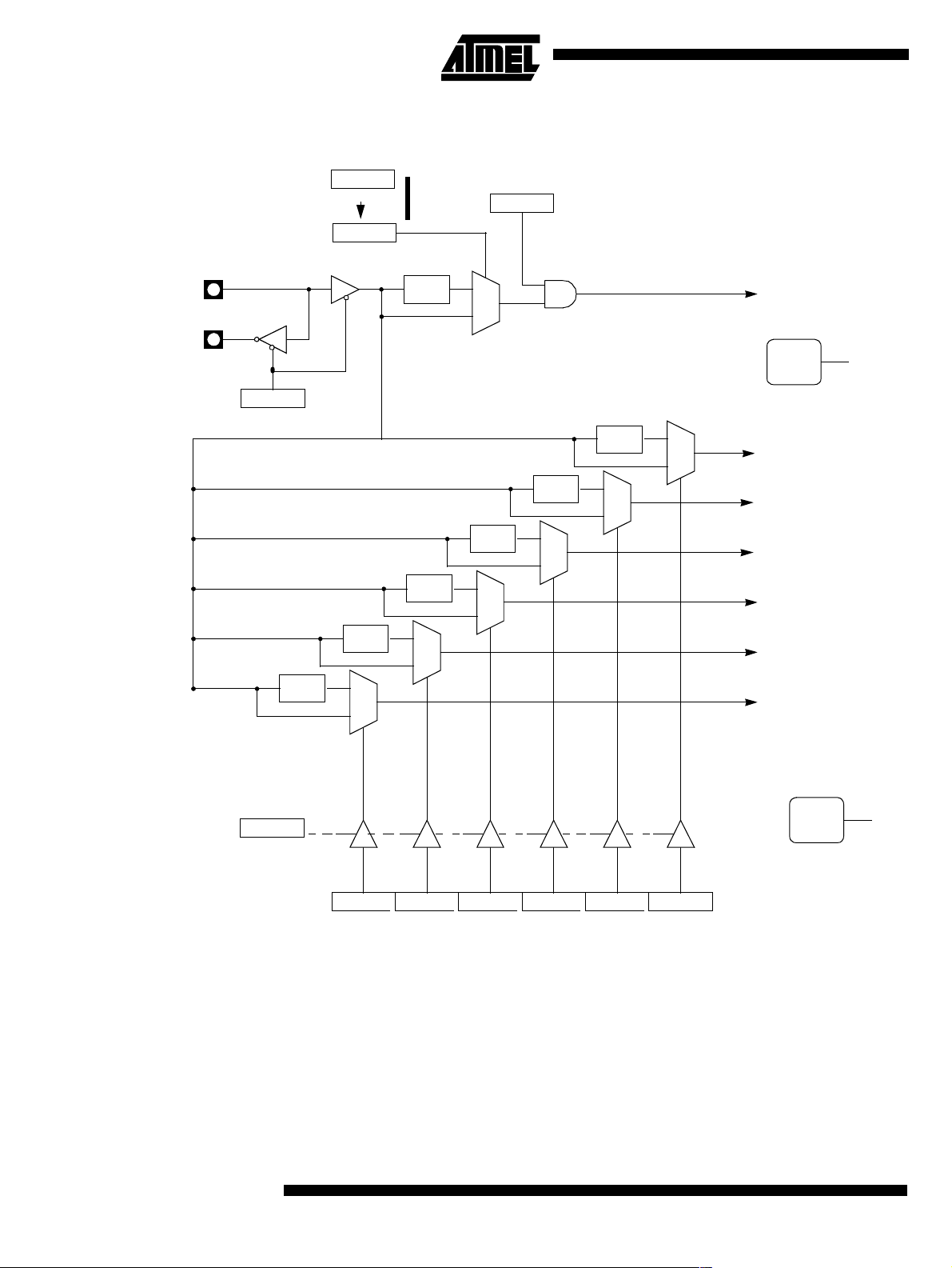
Figure 5. Clock CPU Generation Diagram
XTAL1
XTAL2
PD
PCON.1
÷ 2
X2B
Hardware byte
X2
CKCON.0
÷ 2
1
0
On RESET
÷ 2
÷ 2
1
0
0
1
÷ 2
1
0
PCON.0
IDL
÷ 2
1
0
÷ 2
1
0
CPU Core
Clock
CLOCK
CPU Core Clock Symbol
and ADC
1
0
FT0 Clock
FT1 Clock
FT2 Clock
FUart Clock
FPca Clock
FWd Clock
CPU
16
CKCON.0
T89C51AC2
X2
WDX2
CKCON.6
PCAX2
CKCON.5
SIX2
CKCON.4
T2X2
CKCON.3
T1X2
CKCON.2
PERIPH
CLOCK
Peripheral Clock Symbol
T0X2
CKCON.1
Rev. B – 19-Dec-01
Page 17
XTAL1
XTAL2
X2 bit
CPU clock
T89C51AC2
Figure 6. Mode Switching Waveforms
X2 ModeSTD Mode STD Mode
Note: In order to prevent any incorrect operation while operating in the X2 mode, users must be
aware that all peripheralsusing the clock frequency as a time reference (UART, timers...)
will have their time reference divided by two. For example a free running timer generating
an interrupt every 20 ms will then generate an interrupt every 10 ms. A UART wi th a
4800 baud rate will have a 9600 baud rate.
6.2 Register Table 12. CKCON Register
CKCON (S:8Fh)
Clock Control Register
76543210
- WDX2 PCAX2 SIX2 T2X2 T1X2 T0X2 X2
Bit
Number
6WDX2
5 PCAX2
4SIX2
3T2X2
2T1X2
Bit
Mnemonic Description
Watchdog clock (1)
Clear to select 6 clock periodsper peripheral clock cycle.
Set to select 12 clock periods per peripheral clock cycle.
Programmable Counter Array clock (1)
Clear to select 6 clock periodsper peripheral clock cycle.
Set to select 12 clock periods per peripheral clock cycle.
Enhanced UART clock (MODE 0 and 2) (1)
Clear to select 6 clock periodsper peripheral clock cycle.
Set to select 12 clock periods per peripheral clock cycle.
Timer2 clock (1)
Clear to select 6 clock periodsper peripheral clock cycle.
Set to select 12 clock periods per peripheral clock cycle.
Timer1 clock (1)
Clear to select 6 clock periodsper peripheral clock cycle.
Set to select 12 clock periods per peripheral clock cycle.
Rev. B – 19-Dec-01
Timer0 clock (1)
1T0X2
Clear to select 6 clock periodsper peripheral clock cycle.
Set to select 12 clock periods per peripheral clock cycle.
17
Page 18

Bit
Number
0X2
Bit
Mnemonic Description
CPU clock
Clear to select 12 clock periods per machine cycle (STD mode) for CPU and all
the peripherals.
Set to select6clockperiodspermachine cycle(X2 mode) and to enablethe
individual peripherals "X2"bits.
Notes: 1. This control bit is validated when the CPU clock bit X2 is set; when X2 is low, this bit
has no effect.
Reset Value = 0000 0000b
18
T89C51AC2
Rev. B – 19-Dec-01
Page 19
T89C51AC2
7. Data Memory The T89C51AC2 pro vides data memory access in two different space s:
1. The internal space mapped in three separate segments:
• the lower 128 bytes RAM s egment.
• the upper 128 bytes RAM segment.
• the expanded 1024 bytes RAM s egment (ERAM).
2. The external space.
A fourth internal segment is avail able but ded icated to Speci al Function R egisters,
SFRs, (addresses 80h to
Figure 2 shows the internal and exte rn al data m emory spaces organization.
Figure 1. Internal memory - RAM
FFh) accessible by direct addressing mode.
FFh
128 bytes
Internal RAM
indirect addressing
80h
7Fh
128 bytes
Internal RAM
director indirect
00h
addressing
Upper
Lower
FFh
direct addressing
80h
Special
Function
Registers
Figure 2. Internal and External Data Memory Organization E RAM-XRAM
FFFFh
64 Kbytes
External XRAM
Rev. B – 19-Dec-01
256upto1024bytes
Internal ERAM
EXTRAM= 0
00h
Internal
FFh or 3FFh
EXTRAM= 1
0000h
External
19
Page 20
7.1 Internal Space
7.1.1 Lower 128 Bytes RAM The lower 128 bytes of RAM (see Figure 2) are accessible from address 00h to 7Fh
using direct or indirect addressing modes. The lowest 32 bytes are grouped into 4 banks
of 8 registers (R0 to R7). Two bits RS0 and RS1 in PSW register (see Fig ure 3) select
which bank is in use according to Table 1. This allows more e fficient use of cod e space,
since register instructions are shorter than instructions that use dir ec t addressing, and
can be used for context switching in interrupt service routines .
Table 1. Register Bank Selection
RS1 RS0 Description
0 0 Register bank 0 from 00h to 07h
0 1 Register bank 0 from 08h to 0Fh
1 0 Register bank 0 from 10h to 17h
1 1 Register bank 0 from 18h to 1Fh
The next 16 bytes above the register banks form a block of bit-addressable memory
space. The C51 inst ruction set includes a wide selectio n of singl e-bit in s tructions, and
the 128 bits in this area can be directly addressed by these instructions. The bit
addresses in this area are 00h to 7 Fh.
Figure 3. Lower 128 bytes Internal RAM Organi z ation
7Fh
30h
20h
18h
10h
08h
00h
2Fh
Bit-Addressable Space
(Bit Addresses 0-7Fh)
1Fh
17h
4 Banks of
8Registers
0Fh
R0-R7
07h
7.1.2 Upper 128 Bytes RAM The upper 128 bytes of RAM are accessible from address 80h to FFh us ing only indirect
addressing mode.
7.1.3 Expanded RAM The on-chip 1024 bytes of expanded RAM (ERAM) are ac c es s ible from addres s 0000h
to 03FFh using indirect addressing mode through MOVX instructions. I n this address
range, the bit EXTRAM in AUXR register is used to select the ERAM ( default) or the
XRAM. As s how n in Figure 2 wh en EX TRAM = 0 , the E RAM is se le cte d and wh en
EXTRAM= 1, the XRAM is selected.
The size of ERAM can be configured by XRS1-0 bit in AUXR register (default size is
1024 bytes).
20
Note: Lower 128 bytes RAM, Upper 128 bytes RAM, and expanded RAM are made of volatile
memory cells. This means that the RAM content i s indeterminate after power-up and
must then be initialized properly.
T89C51AC2
Rev. B – 19-Dec-01
Page 21
T89C51AC2
7.2 External Space
7.2.1 Memory Interface The external memory interface comprises the external bus (port 0 and port 2) as well as
the bus control signals (RD#, WR#, and ALE).
Figure 4 shows the structure of the external address bus. P0 carries address A7:0 while
P2 carries address A1 5:8. Data D 7:0 is multiple xe d with A7:0 on P0. Table 2 describes
the external memory interface signals.
Figure 4. External Data Memory Interface Structure
T89C51AC2
ALE
WR#
P2
P0
AD7:0
A15:8
Latch
A7:0
RAM
PERIPHERAL
A15:8
A7:0
D7:0
OERD#
WR
Table 2. External Data Memory Interface Signals
Signal
Name Type Description
A15:8 O
AD7:0 I/O
ALE O
Address Lines
Upper address lines for the external bus.
Address/Data Lines
Multiplexed lower address lines and data for the external
memory.
Address Latch Enable
ALE signals indicates that valid address information are available
on lines AD7:0.
Alternative
Function
P2.7:0
P0.7:0
-
RD# O
WR# O
Read
Read signal output to external data memory.
Write
Write signal output to external memory.
P3.7
P3.6
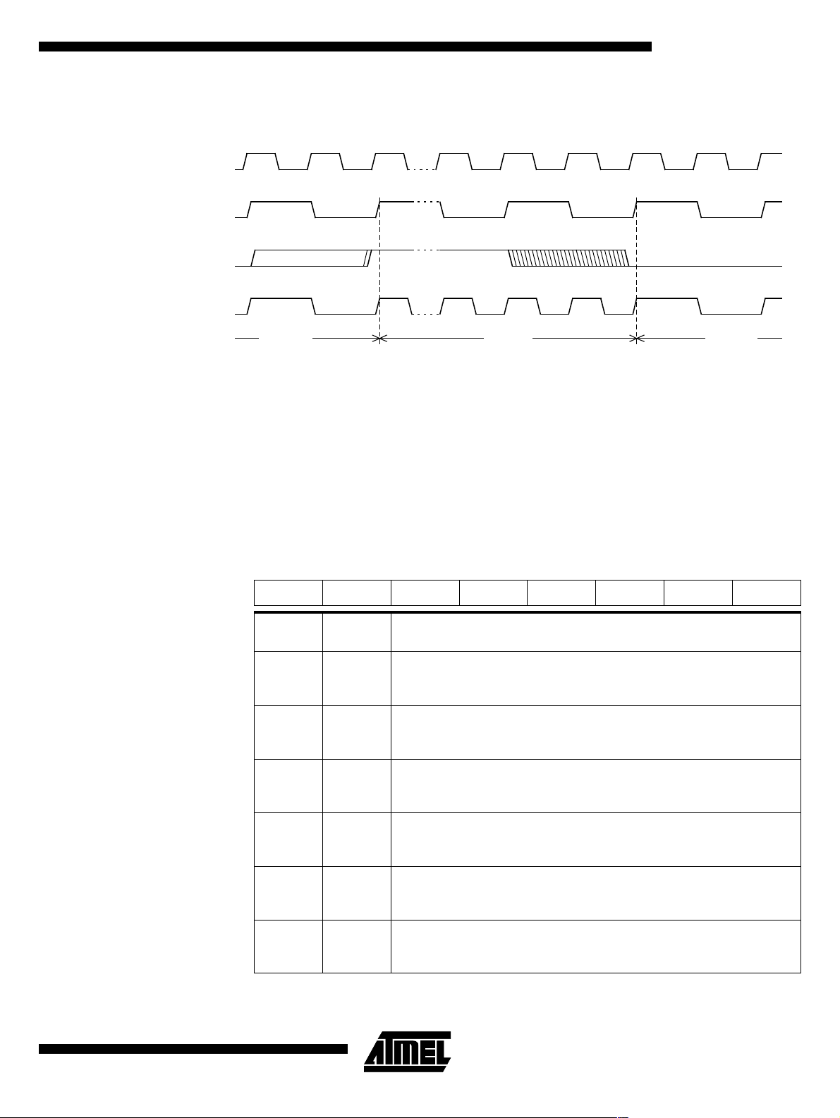
7.2.2 External Bus Cycles This section describes the bus cycles th e T89C51AC2 executes to read (see Figure 5),
and write data (see Figure 6) in the external data m emory.
External m emory cycle takes 6 CPU c lock periods. This is equivalent to 12 oscillator
clock period in standard mode or 6 oscillator clock periods in X2 mode. For further information on X2 mode.
Slow peripherals can be accessed by stretching the read and write cycles. This is done
using the M0 bit in AUXR register. Setting this bit changes the width of the RD# and
WR# signals from 3 to 15 CPU clock periods.
21
Rev. B – 19-Dec-01
Page 22
For simplicity, the accompanying figures depict the bus cycle waveforms in idealized
form and do not provide precise timing information. For bus cycle timing parameters
refer to the Section “AC Characteristics” of the T89C51AC2 datasheet.
Figure 5. External Data Read Waveforms
CPU Clock
ALE
RD#1
P0
P2
Notes: 1. RD# signal may be stretched using M0 bit in AUXR register.
P2
2. When executing MOVX @Ri instruction, P2 outputs SFR content.
DPL or Ri D7:0
DPH or P22
Figure 6. External Data Write Waveforms
CPU Clock
ALE
WR#1
P0
P2
P2
DPL or Ri D7:0
DPH or P22
22
Notes: 1. WR# signal may be stretched using M0 bit in AUXR register.
2. When executing MOVX @Ri instruction, P2 outputs SFR content.
T89C51AC2
Rev. B – 19-Dec-01
Page 23
T89C51AC2
7.3 Dual Data Pointer The T89C51AC2 implements a second data pointer for speeding up code execution and
reducing code size in case of intens ive usage of external memory accesses.
DPTR0 and DPTR1 are seen by the CPU as DPTR and are accessed using the SFR
addresses 83h and 84h that are the DPH and DPL addresses. Th e DPS bit in AUX R1
register (see Figure 5) is used to select whether DPTR is the data pointer 0 or the dat a
pointer 1 (see Figure 7).
Figure 7. Dual Data Pointer Implementation
DPL0
DPL1
DPTR0
DPTR1
DPH0
DPH1
0
1
DPS
0
1
DPL
AUXR1.0
DPH
DPTR
7.3.1 Application Software can take advantage of the additional data pointers to both increase speed and
reduce code size, f or example, block operations ( c opy, compare…) are well served by
using one data pointer as a “source” pointer and the other one a s a “destination” pointer.
Hereafter is an example of block m ove implementation u sing the two pointers and coded
in assembler. The l at est C compi ler t ak es also advantage of this feature by providin g
enhanced algorithm libraries.
The INC instruction is a short (2 bytes) and fast (6 machin e cycle) way to manipulate the
DPS bit in the AUX R1 register. However, note that the INC instruction does not directly
force the DPS bit to a particular state, but simply toggles it. In simple routines, such as
the block move exam ple, only the fact that DPS is toggled in the proper sequence matters, not its actual value. In other words, the block move routine works the same whether
DPS is '0' or '1' on entry.
; ASCII block move using dual data pointers
; Modifies DPTR0, DPTR1, A and PSW
; Ends when encountering NULL character
; Note: DPS exits opposite to the entry state unless an extra INC AUXR1 is
added
Rev. B – 19-Dec-01
AUXR1EQU0A2h
move:movDPTR,#SOURCE ; address of SOURCE
incAUXR1 ; switch data pointers
movDPTR,#DEST ; address of DEST
mv_loop:incAUXR1; switch data pointers
movxA,@DPTR; get a byte from SOURCE
incDPTR; increment SOURCE address
incAUXR1; switch data pointers
movx@DPTR,A; write the byte to DEST
incDPTR; increment DEST address
jnzmv_loop; check for NULL terminator
end_move:
23
Page 24

7.4 Registers Table 3. PSW Register
PSW (S:8Eh)
Program Status Word Register.
76543210
CY AC F0 RS1 RS0 OV F1 P
AUXR (S:8Eh)
Auxiliary Register
Bit
Number
7CY
6AC
5F0User Definable Flag 0.
4-3 RS1:0
2OV
1F1User Definable Flag 1.
0P
Bit
Mnemonic Description
Carry Flag
Carry out from bit 1 of ALU operands.
Auxiliary Carry Flag
Carry out from bit 1 of addition operands.
Register Bank Select Bits
Refer to Table 1 for bitsdescription.
Overflow Flag
Overflow set by arithmetic operations.
Parity Bit
Set when ACC contains anoddnumber of 1’s.
Cleared when ACC contains an even number of 1’s.
Reset Value= 0000 0000b
Table 4. AUXR Register
24
T89C51AC2
76543210
- - M0 - XRS1 XRS0 EXTRAM A0
Bit
Number
7-6 -
5M0
4-
Bit
Mnemonic Description
Reserved
The valueread from these bits are indeterminate.Do not setthis bit.
Stretch MOVX control:
the RD/ and the WR/ pulse length isincreasedaccording to the value of M0.
M0 Pulse length in clock period
06
130
Reserved
The value readfrom this bit is indeterminate.Donot set this bit.
Rev. B – 19-Dec-01
Page 25

T89C51AC2
AUXR1 (S:A2h)
Auxiliary Control Register 1.
Bit
Number
3-2 XRS1-0
1 EXTRAM
0A0
Bit
Mnemonic Description
ERAM size:
Accessiblesize of the ERAM
XRS1:0 ERAM size
0 0 256 bytes
0 1 512 bytes
1 0 768 bytes
1 1 1024 bytes (default)
Internal/External RAM (00h - FFh)
access usingMOVX@ Ri / @ DPTR
0 - Internal ERAM access using MOVX @ Ri / @ DPTR.
1 - External data memory access.
Disable/Enable ALE)
0 - ALE is emitted at a constant rateof 1/6 the oscillatorfrequency(or 1/3 if X2
mode is used)
1-ALEisactiveonlyduringaMOVXorMOVCinstruction.
Reset Value= X00X 1100b
Not bit addressable
Table 5. AUXR1 Register
76543210
- - ENBOOT - GF3 0 - DPS
Bit
Number
7-6 -
5 ENBOOT
4-
3GF3General Purpose Flag 3.
20
1-Reserved for Data Pointer Extension.
0DPS
Bit
Mnemonic Description
Reserved
The value readfrom these bits is indeterminate. Do not set these bits.
Enable Boot Flash
Set this bit for map the boot flash between F800h -FFFFh
Clearthis bit for disable bootflash.
Reserved
The value readfrom this bit is indeterminate.Donot set this bit.
Always Zero
This bit is stuck to logic 0 to allow INC AUXR1 instruction without affecting GF3
flag.
Data Pointer Select Bit
Set to select second dual data pointer: DPTR1.
Clear to select firstdualdata pointer:DPTR0.
Reset Value= XXXX 00X0b
Rev. B – 19-Dec-01
25
Page 26

8. EEPROM Data
Memory
The 2k byte on-chip EEPROM memory block is located at addresses 0000h to 07FFh of
the XR AM /ERAM memory space and is selected by setting control b its in the EECO N
register. A read in the EEPROM memory is done with a MOVX instruction.
A physical write in the EEPROM memory is done in two steps: write data in the column
latches and transfer of all data latches into an EEPROM memory row (programming).
The number of data written on the page may vary from 1 up to 128 bytes (the page
size). When programming, only the data written in the colum n latch is programmed and
a ninth bit is used to obtain this feature. This provides the capability t o program t he
whole memory by by tes, by page or by a number of b ytes in a page. Indeed, each ninth
bit is set when the writing the corresponding byte in a row and all these ninth bits are
reset after the writing of the complete EEPROM row.
8.1 Write Data in the
column latches
Data is written b y byte to the column latches as for an external RAM memory. Out of the
11 address bits of the data pointer, the 4 MSBs are used for page selection (row) and 7
are u sed for byte selection. Between two EEPROM programming sessions, a ll the
addresses in the column latches must stay on t he same page, meaning that the 4 MSB
must no be change d.
The following procedure is used to write to the column latches:
• Save and disable interrupt.
• Set bit EEE of EECO N regi ster
• Load DPTR with the address to write
• Store A regi ster with the data to be written
• Execute a MOVX @DPTR, A
• If needed loop the three last ins tructions until the end of a 128 bytes page
• Restore interrupt.
Note: The last page address used when loading the column latch is the one used to select the
page programming address.
8.2 Programming The EEPROM programming consists on the following actions:
• writing one or more bytes of one page in the column latches. Normally, all by tes
must belong to the same page; if not, the first page address will be latched and the
others discarded.
• launching programming by writing the control seque nc e (50h followed by A0h) to the
EECON register.
• EEBUSY flag in EECON is then set by hardware to indicate that programming is in
progress and that the EEPROM segment is not available for reading.
• The end of programming is indi ca ted by a hardware clear of the EEBUSY flag.
Note: The sequence 5xh and Axh m ust be executed without instructions between then other-
wise the programming is aborted.
8.3 Read Data The following procedure is used to read the data stored in the EEPROM memory:
• Save and disable interrupt
• Set bit EEE of EECO N regi ster
• Load DPTR with the address to read
• Execute a MOVX A, @DPTR
• Restore interrupt
26
T89C51AC2
Rev. B – 19-Dec-01
Page 27

T89C51AC2
8.4 Examples ;*F*************************************************************************
;* NAME: api_rd_eeprom_byte
;* DPTR contain address to read.
;* Acc contain the reading value
;* NOTE: before execute this function, be sure the EEPROM is not BUSY
;***************************************************************************
api_rd_eeprom_byte:
MOV EECON, #02h; map EEPROM in XRAM space
MOVX A, @DPTR
MOV EECON, #00h; unmap EEPROM
ret
;*F*************************************************************************
;* NAME: api_ld_eeprom_cl
;* DPTR contain address to load
;* Acc contain value to load
;* NOTE: in this example we load only 1 byte, but it is possible upto
;* 128 bytes.
;* before execute this function, be sure the EEPROM is not BUSY
;***************************************************************************
api_ld_eeprom_cl:
MOV EECON, #02h ; map EEPROM in XRAM space
MOVX @DPTR, A
MOVEECON, #00h; unmap EEPROM
ret
;*F*************************************************************************
;* NAME: api_wr_eeprom
;* NOTE: before execute this function, be sure the EEPROM is not BUSY
;***************************************************************************
api_wr_eeprom:
MOV EECON, #050h
MOV EECON, #0A0h
ret
Rev. B – 19-Dec-01
27
Page 28

8.5 Registers Table 6. EECON Register
EECON (S:0D2h)
EEPROM Control Register
76543210
EEPL3 EEPL2 EEPL1 EEPL0 - - EEE EEBUSY
Bit
Bit Number
Mnemonic Description
7-4 EEPL3-0
3-
2-
1 EEE
0 EEBUSY
Programming Launch command bits
Write 5Xh followed by AXh to EEPL to launch the programming.
Reserved
The value read from this bit is indeterminate. Do not set this bit.
Reserved
The value read from this bit is indeterminate. Do not set this bit.
Enable EEPROM Space bit
SettomaptheEEPROMspaceduringMOVXinstructions(Writeinthecolumn
latches)
Clear to map the XRAM space during MOVX.
Programming Busy flag
Set by hardware when programming is in progress.
Cleared by hardwarewhenprogramming is done.
Can not be set or clearedbysoftware.
ResetValue=XXXX XX00b
Not bit addressable
28
T89C51AC2
Rev. B – 19-Dec-01
Page 29

T89C51AC2
9. Program/Code
Memory
The T89C51AC2 implement 32 Kbytes of on-chip program/code memory. Figure 8
shows the partitioning of internal and external program/code memory spaces depending
on the product.
The FLASH memory increases EPROM and ROM functionality by in-circuit electrical
erasure and programming. Thanks to th e internal charge pump, t he high voltage needed
for p rogramming or erasi ng FLAS H cells is g enerated on-chip using the standard VDD
voltage. Th us, the FLA SH Memory can be program med using only on e voltage and
allows In-System Programming commonly known as ISP. Hardware programming mode
is also available using specific p ro gramm ing tool.
Figure 8. Program/Code Memory Organization
FFFFh
32 Kbytes
external
memory
8000h
7FFFh
32 Kbytes
internal
FLASH
7FFFh
32 Kbytes
external
memory
EA = 1
0000h
Note: If the program executes exclusively from on-chip code memory (not from external mem-
ory), beware of executing code from the upper byte of on-chip memory (7FFFh) and
thereby disrupt I/O Ports 0 and 2 due to external prefetch. Fetching code constant from
this location does not affect Ports 0 and 2.
0000h
EA = 0
9.1 External Code
Memory Access
9.1.1 Memory Interface The external memory interface comprises the external bus (port 0 and port 2) as well as
the bus control signals (PSEN#, and ALE ).
Figure 9 shows the structure of the external address bus. P0 carries address A7:0 while
P2 carries address A1 5:8. Data D 7:0 is multiple xe d with A7:0 on P0. Table 7 describes
the external memory interface signals.
Rev. B – 19-Dec-01
29
Page 30
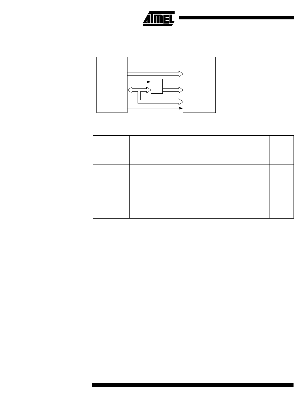
Figure 9. External Code Memory Interface Structure
T89C51AC2
ALE
P2
P0
AD7:0
A15:8
Latch
A7:0
FLASH
EPROM
A15:8
A7:0
D7:0
OEPSEN#
Table 7. External Code Memory Interface Si gnals
Signal
Name Type Description
A15:8 O
AD7:0 I/O
ALE O
PSEN# O
Address Lines
Upper address lines for the external bus.
Address/Data Lines
Multiplexed lower address lines and data for the external memory.
Address Latch Enable
ALE signals indicates that valid address information are available on lines
AD7:0.
Program Store Enable Output
This signal is activelow during external code fetchorexternal code read
(MOVC instruction).
Alternate
Function
P2.7:0
P0.7:0
-
-
9.1.2 External Bus Cycles T his section describes the bus cycles the T89C51AC2 executes to fetch code (s ee
Figure 10) in the external program/cod e memory.
External m emory cycle takes 6 CPU c lock periods. This is equivalent to 12 oscillator
clock period in standard mode or 6 oscillator clock periods in X2 mode. For further information on X2 mode see s ec tion “Clock “.
For simplicity, the accom panying figure de picts the bus cycle waveforms in idealized
form and do not provide precise timing in formation.
For bus cycling parameters refer to the section "AC-DC parameters".
30
T89C51AC2
Rev. B – 19-Dec-01
Page 31

Figure 10. Ex ternal Code Fetch Waveforms
CPU Clock
ALE
PSEN#
T89C51AC2
9.2 FLASH Memory
Architecture
D7:0
P0
P2
T89C51AC2 features two on-ch ip flash m emories:
• Flash memory FM0:
containing 32 Kbytes of program memory (user space) organized into 128 byte
pages,
• Flash memory FM1:
2 Kbytes for boot loader and Application Programming Interfaces (API).
The FM0 c an be program by both parallel programming and S erial In-System Programming (ISP) whereas FM1 supports only parallel programmi ng by programmers. The ISP
mode is detailed in the "In-System P rogramming" section.
All Read/Write access operations on FLASH Memory by user application are managed
by a set of API described in the "In-System Programming" section.
Figure 11. Flash memory architecture
Hardware Security (1 byte)
Extra Row (128 bytes)
Column Latches (128 bytes)
PCL
PCLD7:0 D7:0
PCHPCH
PCH
2Kbytes
Flash memory
boot space
FM1
FFFFh
F800h
Rev. B – 19-Dec-01
7FFFh
0000h
32 Kbytes
Flash memory
user space
FM0
FM1 mapped between FFFFh and
F800h when bit ENBOOT is set in
AUXR1 register
31
Page 32

9.2.1 FM0 Memory
Architecture
The flash memory is made up o f 4 b locks (see Figure 11):
3. The memory array (user space) 32 Kbytes
4. The Extra Row
5. The Hardware security bits
6. The column latch registers
User Space This space is composed of a 32 Kbytes FLASH memory organized in 2 56 pages of 128
bytes. It contains the user’s application code.
Extra Row (X Row) This row is a part of FM0 and has a s ize of 128 bytes . The extra row may contain infor-
mation for boot loader usage.
Hardware security Byte The Hardware security Byte space is a part of FM0 and has a size of 1 byte.
The 4 MS B can be read/written by soft w are, the 4 LSB can only be read by sof t w are and
written by hardware in parallel mode.
Column latches The column latches, also part of FM0, have a size of full page (128 bytes).
The column latches are the entrance buffers of the three previous memory locations
(user array, XROW and Hardware security byte).
9.2.2 Cross Flash Memory
Access Description
The FM0 memory can be program only from FM1. Programming FM0 from FM0 or from
external memory is impossible.
The FM1 memory can be program only by parallel programming.
The Table 8 show all software f lash access allowed.
Table 8. Cross Flash Memory Access
Code executing from
FM0
(user Flash)
FM1
(boot flash)
External
memory
EA = 0
Action
Read ok -
Load column latch ok -
Write - -
Read ok ok
Load column latch ok -
Write ok -
Read - -
Load column latch - -
Write - -
FM0
(user Flash)
FM1
(boot Flash)
32
T89C51AC2
Rev. B – 19-Dec-01
Page 33

T89C51AC2
9.3 Overview of FM0
operations
9.3.1 Mapping of the memor y
space
The CPU interfaces to the flash memory through the FCON register and AUXR1
register.
These registers are used to:
• Map the memory spaces in the adressable space
• Launch the programming of the memory spaces
• Get the status of the flash memory (bus y /not busy)
By default, the user space is accessed by MOVC instruction for re ad only. The column
latches space is m a de accessible by setting the FPS bit in FCON register. Writing is
possible from 0000h to 7FFFh, address bits 6 to 0 are used to select an address within a
page while bits 14 to 7 are used to sele ct the programming address of the page.
Setting FPS bit takes precedence on the EXTRAM bit in AUXR register.
The o th er memory spaces (user, extra row, hardw are security) are made acc es s ible in
the code segment b y program ming bits FMOD0 and FMOD1 in FCON register in accordance with Table 9. A MOVC instruction is then used for reading these spaces.
Table 9. .FM0 blocks select bits
FMOD1 FMOD0 FM0 Adressable space
0 0 User (0000h-FFFFh)
0 1 Extra Row(FF80h-FFFFh)
1 0 Hardware Security Byte (0000h)
11reserved
9.3.2 Launching programming FPL3:0 bits in FCON register are used to secure the launch of programming. A specific
sequence must be written in these bits to unl oc k the write protection and t o launch the
programming. This sequence is 5xh followed by Axh. Table 10 summarizes the memory
spaces to program according to F MOD1:0 bits.
Rev. B – 19-Dec-01
33
Page 34

Table 10. Programming spaces
Write to FCON
5 X 0 0 No action
User
AX00
5 X 0 1 No action
Extra Row
AX01
OperationFPL3:0 FPS FMOD1 FMOD0
Write the column latches in user
space
Write the column latches in extra row
space
9.3.3 Status of the flash
memory
Hardware
Security
Byte
Reserved
Note: The sequence 5xh and Axh must be executing without instructions between them other-
wise the programming is aborted.
Note: Interrupts that may occur during programming time must be disabled to avoid any spuri-
ous exit of the programming mode.
The bit FBUSY in FCON register is used t o indicat e the s ta tus of program ming.
FBUSY is set when programmi ng is in progress.
5 X 1 0 No action
A X 1 0 Write the fuse bits space
5 X 1 1 No action
A X 1 1 No action
9.3.4 Selecting FM1 The bit ENBOOT in AUXR1 register is used to map FM1 from F800h to FFFFh.
9.3.5 Loading the Column
Latches
Any number of data from 1 byte to 128 bytes can be loaded in the column latches. This
provides the capability to program the whole memory by byte, by page or by any number
of bytes in a page.
When programming is launched, an automatic erase of the locations loaded in the column latches is first performed, then programming is effectively done. Thus no page or
block erase is needed an d only the loaded data are programmed in the corresponding
page.
34
The fol lowi ng p ro ced ur e is u se d to l oa d th e co lu mn latches a nd i s su mm a rized in
Figure 12:
• Disable interrupt and map the column latch space by setting FPS bit.
• Load the DPTR with the address t o load.
• Load Accumulator register wi th th e da ta to load.
• Execute the MOVX @DPTR, A instruction.
• If needed loop the three last ins tructions until the page is completely loaded.
• unmap the column latch and Enable Interrupt
T89C51AC2
Rev. B – 19-Dec-01
Page 35

Figure 12. Col umn Latches Loading Procedure
Column Latches
Loading
Save & Disable IT
EA= 0
Column Latches Mapping
FCON = 08h (FPS=1)
Data Load
DPTR= Address
ACC= Data
Exec:MOVX@DPTR,A
Last Byte
to load?
T89C51AC2
Data memory Mapping
FCON = 00h (FPS = 0)
Restore IT
Note: The last page address used when loading the column latch is the one used to select the
page programming address.
9.3.6 Program m in g the FLASH
Spaces
User The followi ng pro ced ure is used to pro gram the User spa ce and is s um mar ize d in
Figure 13:
• Load up to one page of data in the column latches from address 0000h to 7FFFh.
• Disable the interrupts.
• Launch the programming by writing the data sequence 50h followed by A0h in
FCON register (only from FM1).
The end of the programming indicated by the FBUSY flag cleared.
• Enable the interrupts.
Extra Row The following proc edure is used to program the Ex tra Row space and is summ arized in
Figure 13:
• Load data in the column latches from address FF80h to FFFFh.
• Disable the interrupts.
Rev. B – 19-Dec-01
35
Page 36

• Launch the programming by writing the data sequence 52h followed by A2h in
FCON register (only from FM1).
The end of the programming indicated by the FBUSY flag cleared.
• Enable the interrupts.
Figure 13. F lash and Extra row Programming Procedure
FLASH Spaces
Programming
Column Latches Loading
see Figure 12
Save & Disable IT
EA= 0
Launch Programming
FCON= 5xh
FCON= Axh
Hardware Security Byte
FBusy
Cleared?
Clear Mode
FCON = 00h
End Programming
Restore IT
The following procedure is used to program the Hardware Security Byte space
and is summarizedin Figure 14:
• Set FPS and map Hardware byte (F CON = 0x0C)
• Save and disable the interrupts.
• Load DPTR at address 0000h.
• Load Accumulator register wi th th e da ta to load.
• Execute the MOVX @DPTR, A instruction.
• Launch the programming by writing the data sequence 54h followed by A4h in
FCON register (only from FM1).
The end of the programming indicated by t he FBusy flag cleared.
• Restore the interrupts
36
.
T89C51AC2
Rev. B – 19-Dec-01
Page 37

Figure 14. Hardware Programming Procedure
FLASH Spaces
Programming
Save & Disable IT
EA= 0
FCON = 0Ch
T89C51AC2
Save & Disable IT
EA= 0
Launch Programming
FCON= 54h
FCON= A4h
Data Load
DPTR= 00h
ACC= Data
Exec:MOVX@DPTR,A
End Loading
Restore IT
FBusy
Cleared?
Clear Mode
FCON = 00h
End Programming
RestoreIT
9.3.7 Reading the FLASH
Spaces
User The following procedure is used to read t he User space:
• Read one byte in Ac cu mulator by executing MOVC A,@A+DPTR with
A+DPTR=read@.
Note: FCON is supposed to be reset when not needed.
Extra Row The following proc edure is used to read the Extra Row space and is summarized in
Figure 15:
• Map the Extra Row space by writing 02h in FCON register.
• Read one byte in Ac cu mulator by executing MOVC A,@A+DPTR with A= 0 &
DPTR= FF80h to FFFFh.
• Clear FCON to unmap the Extra Row.
Hardware Security Byte
Rev. B – 19-Dec-01
The fo llowing pro c ed ur e is used to re ad the Hardwar e Security space and is
summarized in Figure 15:
• Map the Hardware Secur ity space by writing 04h i n FC ON register.
• Read the byte in Accumulator by executing MOVC A,@A+DPTR with A= 0 &
DPTR= 0000h.
• Clear FCON to unm ap the H ardware Security Byte.
37
Page 38

Figure 15. Reading Procedure
FLASH Spaces
Reading
FLASH SpacesMapping
FCON= 00000xx0b
Data Read
DPTR= Address
Exec:MOVCA,@A+DPTR
ACC= 0
Clear Mode
FCON = 00h
9.3.8 Flash Protection from
Parallel Programming
The three lock bits in Hardware Security Byte (see " I n-System Programming " sec tion)
are program med according to Tabl e 11 provide differe nt level of pro te c t ion f or the onchip code and data located in FM0 and FM1.
The only way to write this bits are the parallel mode. They are set by default to level 4
Table 11. Program Lock bit
Program Lock Bits
Security
level
1UUU
2PUU
3UPU
4 UUP
LB0 LB1 LB2
Protection description
No program lock features enabled. MOVC instruction executed from
external program memory returns non encrypted data.
MOVC instruction executed from external program memory are
disabled from fetching code bytes from internal memory, EA
and latched on reset, and further parallel programming of the Flash is
disabled.
Same as 2, also verify throughparallelprogramming interface is
disabled.
Same as 3, also external execution is disabled if code roll over beyond
7FFFh
is sampled
Program Lock bits
38
U: unprogrammed
P: programmed
WARNING: Security level 2 and 3 should only be programmed after F lash and Core
verification.
T89C51AC2
Rev. B – 19-Dec-01
Page 39

9.4 Registers
FCON RegisterFCON (S:D1h)
FLASH Control Re gister
T89C51AC2
76543210
FPL3 FPL2 FPL1 FPL0 FPS FMOD1 FMOD0 FBUSY
Bit
Number
7-4 FPL3:0
3FPS
2-1 FMOD1:0
0 FBUSY
Bit
Mnemonic Description
Programming Launch Command Bits
Write 5Xh followed by AXh to launch the programming according to FMOD1:0.
(see Table 10.)
FLASH Map Program Space
Set to map the column latch space in the data memory space.
Clear to re-map the data memory space.
FLASH Mode
See Table 9 or Table 10.
FLASH Busy
Set by hardware when programming is in progress.
Clearbyhardwarewhenprogramming is done.
Can not be changed by software.
Reset Value= 0000 0000b
Rev. B – 19-Dec-01
39
Page 40

10. In-System-
Programming (ISP)
With the implementation of the User Space (FM0) and the Boot S pace (FM1) in Flash
technology the T89C51AC2 allows the system engineer the development of applications
with a very high level of flexibility. This flexibility is based on the possibility to alter the
customer program at any s tages of a product’s life:
• Before assembly the 1st personalization of the product by programming in the FM 0
and if needed also a customized Boot loader in the FM1.
Atmel provide also a standard Boot loader by default UART.
• After assembling on the PCB in its final embedded position by serial mode via the
UART.
This In-System-Programming (ISP) allows code modifica tion over the total lifetim e of the
product.
Besides the default Boot loader Atmel provide to the custo mer also all the needed Application-Programming-Interfaces (API) which are needed for the ISP. The API are located
also in the Boot memo r y.
This allow the customer to have a full use of the 32 Kbyte user m emory.
10.1 Flash Programming
and Erasure
There are three methods of program min g the Fl as h memory:
• The Atmel bootloader l ocated in FM1 is activated by the appl ication. Low level API
routines (located in FM1)will be used to program FM0. The interf ac e used f or seria l
downloading to FM0 is the UART. API can be called also by user ’s bootloader
locatedin FM0 at [SBV]00h.
• A further method exist in activating the Atmel boot loader by hardware activation.
• The FM0 can be pro gramm ed also by the parallel mode using a programmer.
Figure 16. F lash Memory Mapping
FFFFh
2KbytesIAP
bootloader
F800h
7FFFh
Custom
Boot Loader
[SBV]00h
FM1
FM1 mapped b etween F800h and FFFFh
when API called
40
32 Kbytes
Flash memory
FM0
0000h
T89C51AC2
Rev. B – 19-Dec-01
Page 41

10.2 Boot Process
T89C51AC2
10.2.1 Software boot process
example
10.2.2 Hardware boot proces s At the falling edg e of RESET, the bit ENBOOT in AUXR1 register is initialized with the
Many algorithms can be used for the software boot process. Before de scribing them,
We give below the descript ion of t he different flags and bytes.
Boot Loader Jump Bit (BLJB):
- This bit indicates if on R ESET the user wants to jump to this application at address
@0000h on FM0 or exec ute the boot loader at address @F 800h on FM1.
- BLJB = 0 on parts delivered with bootloader programmed.
- To read or modify this bit, the APIs are used.
Boot VectorAddress (SBV):
- This byte contains the MSB of the user boot loader address in F M0.
- The default value of SBV is FFh (no user boot loader in FM 0).
- To read or modify this byte, the AP Is are used.
Extra Byte (EB) & Boot Status Byte (BSB):
- These bytes are reserved for customer use.
- To read or modify these bytes, the APIs are used.
value of Boot Loader Jump Bit (BLJB).
Further at the falling edge of RESET if the following conditions (called H ardware condi-
tion) are detected:
• PSEN low,
• EA high,
• ALE high (or not connected).
– After Hardware Condition the FCON register is initialized with the value 00h
and the PC is initialized with F800h (FM1).
The Hardware condition mak es the bootloader to be executed, whatever BLJB value is.
If no hardware condition is detected, the F CON register is initialized with the value F0h.
Check of the BLJB value.
•IfbitBLJB=1:
User application in FM0 will be started at @0000h (standard reset).
•IfbitBLJB=0:
Boot loader will be started at @F800h in FM1.
Rev. B – 19-Dec-01
41
Page 42

Figure 17. Hardware Boot Process Algorithm
Hardware
ENBOOT = 0
PC = 0000h
No
RESET
Hardware
condition?
No
BLJB = = 0
?
Yes
bit ENBOOT in AUXR1 register
is initialized with BLJB.
ENBOOT = 1
PC = F800h
FCON = 00h
Yes
FCON = F0h
ENBOOT = 1
PC = F800h
Software
10.3 ApplicationProgramming-Interface
Application
in FM0
Several Application Program Interface (API) cal ls are availa ble for use by an application
program to permit selective erasing and programming of FLASH pages. A ll calls are
made by functions.
All these APIs are describe in an doc umentation: "In-System Programing: F lash Library
for T89C51CC01".
This is available on the web site.
Boot Loader
in FM1
42
T89C51AC2
Rev. B – 19-Dec-01
Page 43

T89C51AC2
Table 12. List of API
API CALL Description
PROGRAM DATA BYTE Write a byte in flash memory
PROGRAM DATA PAGE Write a page (128 bytes) in flash memory
PROGRAM EEPROM BYTE Write a byte in Eeprom memory
ERASE BLOCK Erase all flash memory
ERASE BOOT VECTOR (SBV) Erase the boot vector
PROGRAM BOOT VECTOR (SBV) Write the boot vector
PROGRAM EXTRA BYTE (EB) Write the extra byte
READ DATA BYTE
READ EEPROM BYTE
READ FAMILY CODE
READ MANUFACTURER CODE
READ PRODUCT NAM E
READ REVISION NUMBER
READ STATUS BIT (BSB) Read the status bit
READ BOOT VECTOR (SBV) Read the boot vector
READ EXTRA BYTE (EB) Read the extra byte
PROGRAM X2 Write the hardware flag for X2 mode
READ X2 Read the hardware flag for X2 mode
PROGRAM BLJB Write the hardware flag BLJB
READBLJB ReadthehardwareflagBLJB
10.4 XROW Bytes Table 13. Xrow mapping
Description Default value Address
Copy of theManufacturer Code 58h 30h
Copy of the Device ID#1: Family code D7h 31h
Copy of theDevice ID#2: Memories sizeandtype F7h 60h
Copy of theDevice ID#3: Name andRevision FFh 61h
Rev. B – 19-Dec-01
43
Page 44

10.5 Hardware Security Byte
Table 14. Hardware Security byte
76543210
X2B BLJB - - - LB2 LB1 LB0
Bit
Number
7X2B
6BLJB
5-3 -
2-0 LB2:0 Lock Bits
Bit
Mnemonic Description
X2 Bit
Set this bit to start in standard mode
Clearthis bit to startinX2mode.
Boot Loader JumpBit
- 1: T o start the user’s application on next RESET (@0000h) located in FM0,
- 0: To startthe boot loader(@F800h) located in FM1.
Reserved
The valueread from these bits are indeterminate.
Default value after erasing chip: FFh
Note: Only the 4 MSB bits can be accessed by software.
Note: The 4 LSB bits can only be accessed by parallel mode.
44
T89C51AC2
Rev. B – 19-Dec-01
Page 45

T89C51AC2
11. Serial I/O Port The T89C51AC2 I/O serial port is compatible w ith the I/O serial port in the 80C52.
It prov ides bot h synch ronous and asynchronous communication modes. It operates as a
Universal Asynchronous Receiver and Transmitter (UART) in three full-duplex modes
(Modes 1, 2 and 3). Asynchronous transmission and reception can occur simultaneously
and at different baud rates
Serial I/O port includes the following enhancements:
• Framing error detection
• Automatic address recognition
Figure 18. Serial I/O Port Block Diagram
IB Bus
11.1 F raming Error Detection
TXD
RXD
SBUF
Transmitter
Write SBUF
Mode0Transmit
RI
TI
SBUF
Receiver
Receive
Shift register
Read SBUF
Load SBUF
Serial Port
Interrupt Request
Framing bit error de tection is provided for the three asynchronous modes. To enable the
framing bit error detection feature, set SMOD0 bit in PCO N register.
Figure 19. Framing Error Block Diagram
RITIRB8TB8RENSM2SM1SM0/FE
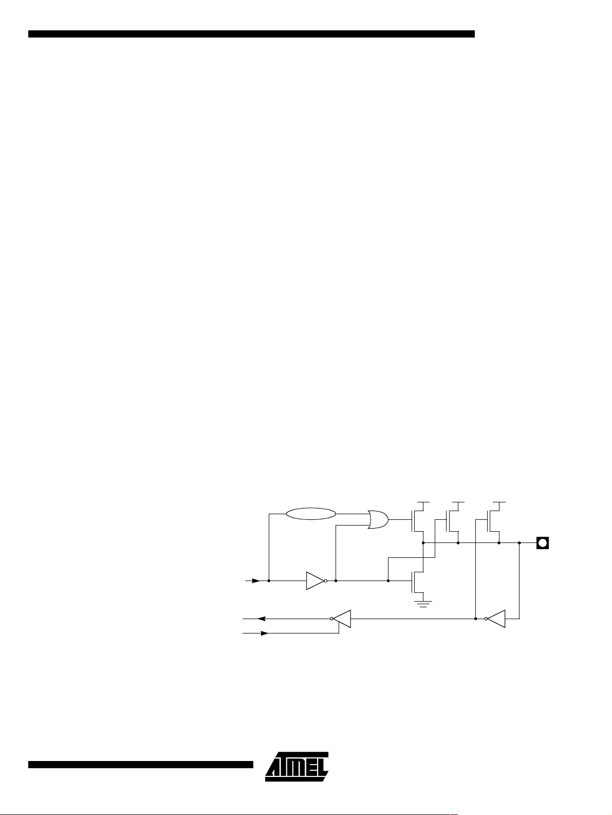
Rev. B – 19-Dec-01
Set FE bit if stop bit is 0 (framing error)
SM0toUARTmodecontrol
IDLPDGF0GF1POF-SMOD0SMOD1
To UART framing error control
When t his feature is enabl ed, the rec eiver checks each incoming data frame for a valid
stop bit. An invalid stop bit may result from noise on the serial lines or from simultaneous
transmission by two CPUs. If a valid stop bit is n ot found, the Framing Error bit (FE) in
SCON register bit is set.
The software may examine the FE bit after each reception to check for data errors.
Once set, o nly software or a reset clears the FE bit. Subsequently received frames with
45
Page 46

valid stop bits cannot clear the FE bit. When t he FE feature is enabled, RI rises on the
stop bit instead of the last data bit (See Figure 20. and Figure 21.).
Figure 20. UART Timing in Mode 1
RXD
RI
SMOD0=X
FE
SMOD0=1
Start
bit
Data byte
Figure 21. UART Timing in Modes 2 and 3
RXD
Start
bit
RI
SMOD0=0
RI
SMOD0=1
FE
SMOD0=1
D7D6D5D4D3D2D1D0
Stop
bit
D8D7D6D5D4D3D2D1D0
Data byte Ninth
bit
Stop
bit
11.2 Automatic Address Recognition
The automatic address recognition f eature is enabled when the multipro ce ssor c ommunication feature is enabled (SM2 bit in SCON register is set).
Implemented in the hardware, automatic address recognition enhances the multiprocessor communication feature by allowing the serial port to examine the address of each
incoming command frame. Only when the serial port recognizes its own address will the
receiver set the RI bit in the SCO N register to generate an interrupt. This ensure s that
the CPU is not interrupted by command frames addressed to other devices.
If neces s ary, you can enable the automatic add ress recognition feature in mode 1. In
this configuration, the stop bit takes the place of the ninth data bit. Bit RI is set only when
the re c eived command frame address matches the device’s address and is termina te d
by a valid stop bit.
To support automatic address recognition, a device is identified by a given address and
a broadcast address.
Note: The multiprocessor communication and automatic address recognition features cannot
be enabled in mode 0 (i.e. settingSM2 bit in SCON register in mode 0 has no effect).
11.3 Given Address E ach device ha s an individual add ress that is specified in the SAD DR register; the
SADEN register is a mas k byte that contains don’t-care bits (defined by zeros) to form
the dev ice’s given address. The don’t-care bits pro v ide the flexibility to address one or
46
T89C51AC2
Rev. B – 19-Dec-01
Page 47

T89C51AC2
more slaves at a time. The following example illustrates how a given address is formed.
To address a device by its individual address, the SADEN mask byte must be 1111
1111b.
For example:
SADDR0101 0110b
SADEN
1111 1100b
Given0101 01XXb
Here is an example of how to use given addresses to address different slaves:
Slave A:SADDR1111 0001b
SADEN
1111 1010b
Given1111 0X0Xb
Slave B:SADDR1111 0011b
SADEN
1111 1001b
Given1111 0XX1b
Slave C:SADDR1111 0010b
SADEN
1111 1101b
Given1111 00X1b
The SADEN byte is se lecte d so that each slave may be addressed separately.
For slave A, b it 0 (the LSB) is a don’t-care bit; for slaves B and C, bit 0 is a 1. To communicate with slave A only, the master must send an address where bit 0 is clear (e.g.
1111 0000b).
For s lave A, bit 1 is a 0; for slaves B and C, bit 1 is a don’t care bit. To communicate with
slaves A and B , but not slave C, the master must send an address with bits 0 and 1 both
set (e.g. 1111 0011b).
To c ommunicate with slaves A, B and C, the master must s end an address with bit 0 set,
bit 1 clear, and bit 2 clear (e.g. 1111 0001b).
11.4 Broadcast Address A broadcast address is formed from the logical O R of the SADDR and SADEN registers
with zeros defined as don’t-care bits, e.g.:
SADDR 0101 0110b
SADEN 1111 1100b
SADDR OR SADEN1111 111Xb
The use of don’t- care bits provides flexibility in defining the broadcast address, however
in mos t applications, a broadcast address is FFh. The following is an example of using
broadcast addresses:
Slave A:SADDR1111 0001b
SADEN
1111 1010b
Given1111 1X11b,
Slave B:SADDR1111 0011b
SADEN
1111 1001b
Given1111 1X11B,
Slave C:SADDR=1111 0010b
SADEN
1111 1101b
Given1111 1111b
For slaves A and B, bit 2 is a don’t care bit; for slave C, bit 2 is set. T o communicat e with
all of the slaves, the master must send an address FFh. To communicate with slaves A
and B, but not slave C, the master can send and addre ss FB h.
Rev. B – 19-Dec-01
47
Page 48

11.5 Registers Table 15. SCON Regist er
SCON (S:98h)
Serial Control Register
76543210
FE/SM0 SM1 SM2 REN TB8 RB8 TI RI
Bit
Number
7FE
6SM1
5SM2
4REN
3TB8
2RB8
Bit
Mnemonic Description
SM0
Framing Error bit (SMOD0=1)
Cleartoresettheerrorstate,notclearedbyavalidstopbit.
Set by hardware when an invalid stop bit is detected.
Serial port Mode bit 0 (SMOD0=0)
Refer to SM1for serial port mode selection.
Serial port Mode bit 1
SM0
0 0 Shift Register F
0 1 8-bit UART Variable
1 0 9-bit UART F
1 1 9-bit UART Variable
Serial port Mode 2 bit / Multiprocessor Communication Enable bit
Clearto disable multiprocessor communication feature.
Set to enable multiprocessor communication feature in mode 2 and 3.
Reception Enablebit
Clearto disable serial reception.
Set to enable serial reception.
Transmitter Bit 8 / Ninth bit to transmit in modes 2 and 3
Clearto transmit a logic 0 in the 9th bit.
Set to transmit a logic 1 in the 9th bit.
Receiver Bit 8 / Ninth bitreceived in modes 2 and 3
Cleared by hardwareif9th bit receivedisa logic 0.
Set by hardware if 9th bit received is a logic1.
SM1 Mode BaudRate
XTAL
XTAL
/12 (orF
/64 or F
/6 in mode X2)
XTAL
/32
XTAL
48
T89C51AC2
TransmitInterruptflag
1TI
0RI
Clear to acknowledgeinterrupt.
Set by hardware at the end of the 8th bit time in mode 0 or at the beginning of the
stop bit in theother modes.
Receive Interrupt flag
Clear to acknowledgeinterrupt.
Set by hardware at the end of the 8thbittime in mode 0, see Figure 20.and
Figure 21. in the other modes.
Reset Value = 0000 0000b
Bit addressable
Rev. B – 19-Dec-01
Page 49

SADEN (S:B9h)
Slave Address Mask Register
T89C51AC2
Table 16. SADEN Register
76543210
SADDR (S:A9h)
Slave Address Register
Bit
Number
7-0 Mask Data for Slave Individual Address
Bit
Mnemonic Description
Reset Value = 0000 0000b
Not bit addressable
Table 17. SADDR Register
76543210
Bit
Number
7-0 SlaveIndividualAddress
Bit
Mnemonic Description
Reset Value = 0000 0000b
Not bit addressable
Table 18. SBUF Register
SBUF (S:99h)
Serial Data Buffer
Rev. B – 19-Dec-01
76543210
Bit
Number
7-0 Data sent/received by Serial I/O Port
Bit
Mnemonic Description
Reset Value = 0000 0000b
Not bit addressable
49
Page 50

PCON (S:87h)
Power Control Register
Table 19. PCON Register
76543210
SMOD1 SMOD0 - POF GF1 GF0 PD IDL
Bit
Number
7SMOD1
6SMOD0
5-
4POF
3GF1
2GF0
1PD
0IDL
Bit
Mnemonic Description
Serial port Mode bit 1
Settoselectdoublebaudrateinmode1,2or3.
Serial port Mode bit 0
Clear to select SM0 bit in SCON register.
Set to select FE bit in SCON register.
Reserved
The value readfrom this bit is indeterminate. Do not set this bit.
Power-Off Flag
Clear to recognize next reset type.
Set by hardware when VCC risesfrom 0 to its nominal voltage. Can also be set
by software.
General purpose Flag
Cleared by user for general purpose usage.
Set by user for general purpose usage.
General purpose Flag
Cleared by user for general purpose usage.
Set by user for general purpose usage.
Power-Down mode bit
Cleared by hardwarewhenreset occurs.
Set to enter power-down mode.
Idle mode bit
Clear by hardware when interrupt or reset occurs.
Set to enter idle mode.
50
Reset Value = 00X1 0000b
Not bit addressable
T89C51AC2
Rev. B – 19-Dec-01
Page 51

T89C51AC2
12. Timers/Counters The T89C51AC2 implements two general-purpose, 16-bit Timers/Counters. Such are
identified as Timer 0 and Ti mer 1, and can b e independe ntly configured to operate in a
variety of mode s as a Time r or an eve nt Count e r. When op erating as a T ime r, the
Timer/Counter ru ns for a p rogrammed length of t ime, th en issues an interrupt request.
When operating as a Counter, the Timer/Counter counts negative t ransitions on an
external pin. After a preset numbe r of counts, the Counter issues an interrupt request.
The various o perat ing modes of each Timer/Coun ter are described in the following
sections.
12.1 Timer/Counter Operations
A basic operation is Timer registers THx and TLx (x= 0, 1) co nnected in casc ade to form
a 16-bit Timer. Setting the run co nt rol bit (TRx) in TCON register (see Figure 20) turns
the Timer on by allowing the selected input to increment TLx. When TLx overflows it
increments THx; when THx overflows it sets the Timer overflow flag (TFx) in TCON register. Settin g the TRx does not clear the THx and TLx Timer registers. T im er registers
can be accessed to obtain the current count or to enter preset value s. They can be read
at any time but TRx b it mus t be cleared to preset their values, otherwi se the behavior of
the Timer/Counter is unpre dicta ble.
The C/Tx# control bit selects Timer operation or Counter operation by selecting the
divided-down peripheral clock or external pin Tx as the source for the counted signal.
TRx bit must be cleared when changing the mode of operation, otherwise the behavior
of the Timer/Counter is unpredict able.
For T im er op eration (C/Tx#= 0), the Timer register counts the divided-down peripheral
clock. The Timer register is incremented once every peripheral cycle (6 peripheral clock
periods). The Timer clock rate is F
/6,i.e.F
PER
/ 12 in standard mode or F
OSC
OSC
/6in
X2 mode.
For Count er operation ( C/Tx#= 1), the Timer register counts the negative transitions on
the Tx external input pin. The e xterna l input is sa m pled every pe riphera l cycles. When
the sample is high in one cycle and low in the next one, the Counter is incremented.
Since it takes 2 cycl es (12 peripheral clock periods) to re cogn ize a negative transition,
the maximum count rate is F
/ 12, i.e. F
PER
/ 24 in standard mode or F
OSC
/12inX2
OSC
mode. There are no restrictions on the duty c ycle of the external input s ignal, but to
ensure that a g iven level is sampled at least onc e before it changes, it s hould be held for
at least one full peripheral cycle.
12.2 Timer 0 Timer 0 functions as either a Timer or event Counter in four modes of operation.
Figure 22 to Figure 25 show the logical configuration of each mode.
Timer 0 is controlled by the four lowe r bits of TMO D register (see Figure 21) and bits 0,
1, 4 and 5 of TCON r egister (see Figure 20). TMOD register selects the method of Timer
gating (GATE0 ), Timer or Counter opera tion (T/C0#) and mode of operation (M10 and
M00). TCON register provides T ime r 0 c ontrol func t ions: overflow flag (TF0), run control
bit (TR0), interrupt flag (IE0) and interrupt type control bit (IT0).
For normal T im er operat ion (GATE0= 0) , setting TR0 allows TL0 to be incremented by
the selected input. Settin g GATE0 and TR0 allows external pin INT0# to control Tim er
operation.
Timer 0 overflow (count rolls over from all 1s to all 0s) sets TF0 flag generating an interrupt request.
It is important to stop Timer/Counter before changing mode.
12.2.1 Mode 0 (13-bit Timer) Mode 0 configures Timer 0 as an 13-bit Timer which is set up as an 8-bit Timer (TH0
register) with a modulo 32 prescaler implemented with the lower five bits of TL0 register
(see Figure 22). The uppe r three bi ts of TL0 reg ister are indeterminate and should be
ignored. Prescaler overflow increments TH0 register.
51
Rev. B – 19-Dec-01
Page 52

see section “Clock”
Figure 22. T im er/Cou nter x (x= 0 or 1) in Mode 0
FTx
CLOCK
÷ 6
0
1
THx
(8 bits)
TLx
(5 bits)
Overflow
TFx
TCON reg
Timer x
Interrupt
Request
Tx
C/Tx#
TMOD reg
INTx#
GATEx
TMOD reg
TRx
TCON reg
12.2.2 Mode 1 (16-bit Timer) Mode 1 configures Timer 0 as a 16-bit Timer with TH0 and TL 0 registers connected in
cascade (see Figure 23). The s elect ed i nput increments TL0 register.
Figure 23. T im er/Cou nter x (x= 0 or 1) in Mode 1
see section “Clock”
FTx
CLOCK
Tx
INTx#
÷ 6
0
1
C/Tx#
TMOD reg
THx
(8 bits)
TLx
(8 bits)
Overflow
TFx
TCON reg
Timer x
Interrupt
Request
GATEx
TMOD reg
12.2.3 Mode 2 (8-bit Timer with
Auto-Reload)
see section “Clock”
FTx
CLOCK
Tx
INTx#
GATEx
TMOD reg
TRx
TCON reg
Mode 2 configures Timer 0 as an 8-bit Timer (TL0 register) that automatically reloads
from TH0 register (see Figure 24). TL0 overflow sets TF0 flag in TCON register and
reloads TL0 with the contents of TH0, w hich is preset by software. When the interrupt
request is serviced, hardware clears TF0. The reload leaves TH0 unchanged. The next
reload value may be changed at any time by writing it to TH0 register.
Figure 24. T im er/Cou nter x (x= 0 or 1) in Mode 2
÷ 6
0
1
C/Tx#
TMOD reg
TCON reg
TRx
TLx
(8 bits)
THx
(8 bits)
Overflow
TFx
TCON reg
Timer x
Interrupt
Request
52
T89C51AC2
Rev. B – 19-Dec-01
Page 53

T89C51AC2
12.2.4 Mode 3 (Two 8-bit
Timers)
FTx
CLOCK
T0
INT0#
FTx
CLOCK
see section “Clock”
GATE0
TMOD.3
Mode 3 configures Timer 0 such that registers TL0 and TH0 ope rat e as separate 8-b it
Timers (see Figure 25). This mode is provided for applications requiring an additional 8bit Timer or Counter. TL0 uses the Timer 0 control bits C/T0# and GATE 0 in TMOD register, and TR0 and TF0 in TCON register in the normal manner. TH0 is locked into a
Timer function (counting F
/6) and takes over use of the Tim er 1 interrupt (TF1) and
PER
run control (TR1) bits. Thus, operat ion of Timer 1 is restricted w hen Timer 0 is in mode
3.
Figure 25. T im er/Cou nter 0 in Mode 3: Two 8-bit Counters
÷ 6
÷ 6
0
1
C/T0#
TMOD.2
TR0
TCON.4
TR1
TCON.6
TL0
(8 bits)
TH0
(8 bits)
Overflow
Overflow
TF0
TCON.5
TF1
TCON.7
Timer 0
Interrupt
Request
Timer 1
Interrupt
Request
12.3 Timer 1 Timer 1 is identical to Timer 0 excepted for Mo de 3 which is a hold-count mode. Fol low-
ing comments help to unders tand the differences:
• Timer 1 functions as either a Timer or event Counter in three modes of operation.
Figure 22 to Figure 24 show the logical configuration for modes 0, 1, and 2. Timer
1’s mode 3 is a hold-count mode.
• Timer 1 is c ontrolled by the four high-order bits of TMOD register (see Figure 21)
and bits 2, 3, 6 and 7 of TCON register (see Figure 20). T MOD register selects the
method of Timer gating (GATE1), Timer or Counter operation (C/T1#) and mode of
operation (M11 and M01). TCON register provides Timer 1 control functions:
overflow flag (TF1), run control bit (TR1), interrupt flag (IE1) and interrupt type
control bit (IT1).
• Timer 1 can serve as the Baud Rate Generat or for the Serial Port. Mode 2 is best
suited for this purpose.
• For normal Timer operation (GATE1= 0), setti ng TR 1 allows TL1 to be incremented
by the selected input. Setting GATE1 and TR1 allows external pin INT1# to control
Timer operation.
• Timer 1 overflow (count rolls over from all 1s to all 0s) sets the TF 1 flag generating
an interrupt request.
• When Timer 0 is in mode 3, it uses Timer 1’s overflow flag (TF1) and run control bit
(TR1). For this situation, use Timer 1 only for applications that do not require an
interrupt (such as a Baud Rate Generator for the Serial Po rt) and switch Timer 1 in
and out of mode 3 to turn it off and on.
• It is important to stop Timer/Counter before changing mode.
Rev. B – 19-Dec-01
53
Page 54

12.3.1 Mode 0 (13-bit Timer) Mode 0 configures Timer 1 as a 13-bit Timer, which is set up as an 8-bit Tim er (TH1 reg-
ister) with a modulo-32 prescaler implemented with the lower 5 bits of the TL1 register
(see Fig ure 22). The upper 3 bits of TL1 register are ignore d. Prescaler overflow i nc rements TH1 register.
12.3.2 Mode 1 (16-bit Timer) Mode 1 configures Timer 1 as a 16-bit Timer with TH1 and TL 1 registers connected in
cascade (see Figure 23). The s elect ed i nput increments TL1 register.
12.3.3 Mode 2 (8-bit Timer with
Auto-Reload)
Mode 2 co nfigures Timer 1 as an 8-bit Timer (TL1 register) with automatic reload from
TH1 register on overflow (see Figure 24). TL1 overflow sets TF1 flag in TCON register
and reloads TL1 with the cont ents of TH1, which i s preset by softw are. The reload
leaves TH1 unchanged.
12.3.4 Mode 3 (Halt) Placing Ti mer 1 in mode 3 cause s it to halt and hold its count. This can be used to halt
Timer 1 when TR1 run cont rol bit is not available i.e. when Timer 0 is in mode 3.
12.4 Interrupt Each Timer handles one interrupt source that is the timer overflow flag TF0 or TF1. This
flag is set every time an overflow occurs. Flags are cleared when vectoring to the Tim er
interrupt routine. Interrupts are enabled by setting
interrupts are globally enabled by setting EA bit in IEN0 register.
Figure 26. Timer Interrupt System
TF0
TCON.5
ET0
IEN0.1
TF1
TCON.7
ET1
IEN0.3
Timer 0
InterruptRequest
Timer 1
InterruptRequest
ETx bit in IEN0 register. This assumes
54
T89C51AC2
Rev. B – 19-Dec-01
Page 55

12.5 Registers Table 20. TCON Register
TCON (S:88h)
Timer/Counter Control Register
76543210
TF1 TR1 TF0 TR0 IE1 IT1 IE0 IT0
T89C51AC2
Bit
Number
7TF1
6TR1
5TF0
4TR0
3IE1
2IT1
1IE0
Bit
Mnemonic Description
Timer 1 Overflow Flag
Cleared by hardwarewhenprocessor vector s to interrupt routine.
Set by hardware on Timer/Counter overflow, when Timer 1 register overflows.
Timer 1 Run Control Bit
Clear to turnoff Timer/Counter 1.
SettoturnonTimer/Counter1.
Timer 0 Overflow Flag
Cleared by hardwarewhenprocessor vector s to interrupt routine.
Set by hardware on Timer/Counter overflow, when Timer 0 register overflows.
Timer 0 Run Control Bit
Clear to turnoff Timer/Counter 0.
SettoturnonTimer/Counter0.
Interrupt1 Edge Flag
Cleared by hardware when interrupt is processed if edge-triggered (see IT1).
Set by hardware when external interrupt is detected on INT1# pin.
Interrupt 1 Type Control Bit
Clear to select low levelactive (level triggered) for external interrupt1 (INT1#).
Set to select falling edge active (edge triggered) for external interrupt 1.
Interrupt0 Edge Flag
Cleared by hardware when interrupt is processed if edge-triggered (see IT0).
Set by hardware when external interrupt is detected on INT0# pin.
Rev. B – 19-Dec-01
Interrupt 0 Type Control Bit
0IT0
Clear to select low levelactive (level triggered) for external interrupt0 (INT0#).
Set to select falling edge active (edge triggered) for external interrupt 0.
Reset Value= 0000 0000b
55
Page 56

TMOD (S:89h)
Timer/Counter Mode Control
Register.
Table 21. TMOD Register
76543210
GATE1 C/T1# M11 M01 GATE0 C/T0# M10 M00
Bit
Number
7GATE1
6C/T1#
5M11Timer 1 Mode Select Bits
4M01
3GATE0
2C/T0#
1M10
0
Bit
Mnemonic Description
Timer 1 Gating Control Bit
Clearto enable Timer 1 whenever TR1 bit is set.
Set to enable Timer 1 only while INT1# pin is high and TR1 bit is set.
Timer 1 Counter/Timer Select Bit
Clear forTimer operation: Timer 1 counts the divided-down system clock.
Set forCounter operation: Timer 1 counts negativetransitionsonexternal pinT1.
M11
M01 Operating mode
0 0 Mode 0: 8-bitTimer/Counter (TH1) with 5-bit prescaler (TL1).
0 1 Mode 1: 16-bit Timer/Counter.
1 0 Mode 2: 8-bit auto-reload Timer/Counter (TL1).
1 1 Mode 3: Timer1halted. Retains count.
Timer 0 Gating Control Bit
Clearto enable Timer 0 whenever TR0 bit is set.
Set to enable Timer/Counter 0 only while INT0# pin is high and TR0 bit is set.
Timer 0 Counter/Timer Select Bit
Clear forTimer operation: Timer 0 counts the divided-down system clock.
Set forCounter operation: Timer 0 counts negativetransitionsonexternal pinT0.
Timer 0 Mode Select Bit
M00 Operating mode
M10
0 0 Mode 0: 8-bitTimer/Counter (TH0) with 5-bit prescaler (TL0).
0 1 Mode 1: 16-bit Timer/Counter.
M00
1 0 Mode 2: 8-bit auto-reload Timer/Counter (TL0).
1 1 Mode 3: TL0 is an 8-bit Timer/Counter.
TH0 is an 8-bit Timer using Timer 1’s TR0 and TF0 bits.
(a)
(b)
56
a. Reloaded from TH1 at overflow.
b. Reloaded from TH0 at overflow.
Reset Value= 0000 0000b
T89C51AC2
Rev. B – 19-Dec-01
Page 57

TH0 (S:8Ch)
Timer 0 High Byte Register
T89C51AC2
Table 22. TH0 Register
76543210
TL0 (S:8Ah)
Timer 0 Low Byte Register
TH1 (S:8Dh)
Timer 1 High Byte Register
Bit
Number
7:0 High Byte of Timer 0.
Bit
Mnemonic Description
Reset Value= 0000 0000b
Table 23. TL0 Register
76543210
Bit
Number
7:0 Low Byte of Timer 0.
Bit
Mnemonic Description
Reset Value= 0000 0000b
Table 24. TH1 Register
Rev. B – 19-Dec-01
76543210
Bit
Number
7:0 High Byte of Timer 1.
Bit
Mnemonic Description
Reset Value= 0000 0000b
57
Page 58

TL1 (S:8Bh)
Timer 1 Low Byte Register
Table 25. TL1 Register
76543210
Bit
Number
7:0 Low Byte of Timer 1.
Bit
Mnemonic Description
Reset Value= 0000 0000b
58
T89C51AC2
Rev. B – 19-Dec-01
Page 59

T89C51AC2
13. Timer 2 The T89C51AC2 timer 2 is compatible with timer 2 in the 80C52.
It is a 16-bit timer/counter: the count is maintained by two eight-bit timer registers, TH2
and TL2 that are cascade- connec t ed. I t is contr olled by T2CON register (S ee Table )
and T2MOD register (See Table 28). Timer 2 operation is similar to Timer 0 and Timer
1. C/T2
timer clock. Setting TR2 allows TL2 to be incremented by the selec ted input.
Timer 2 includes the following enhanc ements:
• Auto-reload mode (up or down co unter)
• Programmable clock-output
13.1 Auto-Reload Mode The auto-reload mode configures timer 2 as a 16-bit timer or event counter with auto-
matic reload. T his f eature is controlled by the DCEN bit in T2MOD register (See
Table 28 ). S e ttin g the D CEN bit enab les t im er 2 to count up or down as s how n i n
Figure 27. In this mode the T2EX pin controls the counting direction.
When T2EX is high, tim er 2 counts up . Timer overflow occurs at FFFFh which sets the
TF2 flag and generates an interrupt request. The overflow also c aus es the 16-bit val ue
in RCAP2H and RCAP2L registers to be loaded into the timer registers TH2 and TL2.
When T2EX is low, tim er 2 counts down. Timer underflow occurs when the count in the
timer registers TH2 and TL 2 equals the value stored in RCA P2 H and RCAP2L registers.
The underflow sets TF2 flag and reloads FFFFh into the timer registers.
selects F
/6 (timer operation) or external pin T2 (c ounter operation) as
T2 clock
The EXF2 bit t oggles when timer 2 overflow or underflow, depending on the direc t ion of
the c ount. EXF2 does not generate an interrupt. This bit c an be used to provide 17-bit
resolution.
Rev. B – 19-Dec-01
59
Page 60

Figure 27. Aut o-Reload Mode Up/Down Counter
see section “Clock”
T2
FT2
CLOCK
:6
0
1
CT/2
T2CON.1
(DOWN COUNTING RELOAD VALUE)
FFh
(8-bit)
TL2
(
8-bit)
RCAP2L
(8-bit)
(UP COUNTING RELOAD VALUE)
FFh
(8-bit)
TH2
(8-bit)
RCAP2H
(8-bit)
TR2
T2CON.2
T2EX:
1=UP
2=DOWN
TOGGLE
TF2
T2CONreg
T2CONreg
EXF2
TIMER 2
INTERRUPT
13.2 Programmable Clock-Output
In clock-out mode, timer 2 operat es as a 50%-duty-cycle, programmable clock generator (See Figure 28). T he input clock increments TL2 at frequency F
/2. The timer
OSC
repeatedly counts to overflow from a loaded value. At overflow, the contents of RCAP2H
and RCAP2L registers are loaded into TH2 and TL2. In t his mode, timer 2 overflows do
not generate interrupts. The formula gives the clock-out frequency depending on the
system oscillator frequency and the value in the RCAP2H and RCAP2L registers:
Clock O utFr equen cy–
For a 16 MHz system clock in x1 mode, timer 2 has a program mable frequency range of
61 Hz (F
OSC
16)
/2
to 4 MHz (F
------------------------------------------------------------------------------------------- -
=
4 65536 RCAP2H– RCAP2L⁄()×
/4). The generated clock signal is brought out to T2 pin
OSC
FT2clock
(P1.0).
Timer 2 is programmed for the clock - out m ode as follows:
• Set T2OE bit in T2MOD register.
• Clear C/T2
bit in T2CON register.
• Determine the 16-bit r eload value from the formula and enter it in RCAP2H/RCAP2L
registers.
• Enter a 16-bit initial value in timer registers TH2/TL2. It can be the same as the
reload value or different depending on the a pplicat ion.
• To start the timer, set TR2 run control bit in T2CON register.
60
T89C51AC2
Rev. B – 19-Dec-01
Page 61

T89C51AC2
It is possible to use timer 2 as a baud rate generator and a clock generator s imultaneously. For this configuration, the baud rates and clock frequencies are not
independent since both functions use the values in the R CAP2H an d RCAP2 L registers.
Figure 28. Cl ock-Out Mode
FT2
CLOCK
T2EX
T2
1
0
C/T2
T2CONreg
0
1
CT/2
T2CON.1
TR2
T2CON.2
:2
EXEN2
T2CON reg
TL2
(8-bit)
RCAP2L
(8-bit)
T2OE
T2MOD reg
EXF2
T2CON reg
TH2
(8-bit)
RCAP2H
(8-bit)
OVERFLOW
TIMER2
INTERRUPT
Rev. B – 19-Dec-01
61
Page 62

13.3 Registers Table 26. T2CON Register
T2CON (S:C8h)
Timer 2 Control Register
76543210
TF2 EXF2 RCLK TCLK EXEN2 TR2 C/T2# CP/RL2#
Bit
Number
7TF2
6EXF2
5RCLK
4TCLK
3 EXEN2
2TR2
Bit
Mnemonic Description
Timer 2 overflow Flag
TF2 is not set if RCLK=1 or TCLK = 1.
Must be cleared by software.
Setbyhardwareontimer2overflow.
Timer 2 External Flag
Set when a capture or a reload is causedbya negative transitiononT2EXpinif
EXEN2=1.
Set to causethe CPU to vector totimer 2 interrupt routine when timer2interrupt
is enabled.
Must be cleared by software.
Receive Clock bit
Clear to use timer1 overflow as receiveclockfor seria l port in mode 1 or 3.
Set to use timer 2 overflow as receive clock for serial port in mode 1 or 3.
TransmitClock bit
Clear to use timer1 overflow as transmit clock for serial portinmode1 or 3.
Set to use timer 2 overflow as transmit clock for serial port in mode 1 or 3.
Timer 2 External Enable bit
Clearto ignore eventson T2EX pin for timer2operation.
SettocauseacaptureorreloadwhenanegativetransitiononT2EXpinis
detected, if timer2is notusedtoclock the serialport .
Timer 2 Run control bit
Clear to turnoff timer 2.
Settoturnontimer2.
62
T89C51AC2
Timer/Counter 2 select bit
1C/T2#
0CP/RL2#
Clear fortimer operation ( input from internal clock system: F
Set forcounter operation (input from T2 inputpin) .
Timer 2 Capture/Reload bit
If RCLK=1or TCLK=1, CP/RL2# is ignored and timeris forcedtoauto-reload on
timer2 overflow.
Cleartoauto-reload on timer2 overflowsornegative transitions on T2EX pin if
EXEN2=1.
Set to capture on negative transitions on T2EX pin if EXEN2=1.
Reset Value = 0000 0000b
Bit addressable
).
OSC
Rev. B – 19-Dec-01
Page 63

T2MOD (S:C9h)
Timer 2 Mode Control Register
T89C51AC2
Table 27. T2MOD Register
76543210
------T2OEDCEN
Bit
Number
7-
6-
5-
4-
3-
2-
1T2OE
0 DCEN
Bit
Mnemonic Description
Reserved
The value readfrom this bit is indeterminate. Do not set this bit.
Reserved
The value readfrom this bit is indeterminate. Do not set this bit.
Reserved
The value readfrom this bit is indeterminate. Do not set this bit.
Reserved
The value readfrom this bit is indeterminate. Do not set this bit.
Reserved
The value readfrom this bit is indeterminate. Do not set this bit.
Reserved
The value readfrom this bit is indeterminate. Do not set this bit.
Timer 2 Output Enable bit
Clear to program P1.0/T2 as clock input or I/O port.
Set to program P1.0/T2asclock output .
Down Counter Enabl e bit
Cleartodisable timer 2 as up/down counter.
Set to enable timer 2 as up/down counter.
Reset Value = XXXX XX00b
Not bit addressable
TH2 (S:CDh)
Timer 2 High Byte Register
Rev. B – 19-Dec-01
Table 28. TH2 Register
76543210
--------
Bit
Number
7-0 HighByteofTimer2.
Bit
Mnemonic Description
Reset Value = 0000 0000b
Not bit addressable
63
Page 64

TL2 (S:CCh)
Timer 2 Low Byte Register
Table 29. TL2 Register
76543210
--------
RCAP2H (S:CBh)
Timer 2 Reload/Capture High
Byte Register
Bit
Number
7-0 Low Byte of Timer 2.
Bit
Mnemonic Description
Reset Value = 0000 0000b
Not bit addressable
Table 30. RCAP2H Register
76543210
--------
Bit
Number
7-0 High Byte of Timer 2 Reload/Capture.
Bit
Mnemonic Description
Reset Value = 0000 0000b
Not bit addressable
RCAP2L (S:CA
T
IMER 2REload/Capture Low
H)
Byte Register
64
T89C51AC2
Table 31. RCAP2L Register
76543210
--------
Bit
Number
7-0 Low Byteof Timer 2 Reload/Capture.
Bit
Mnemonic Description
Reset Value = 0000 0000b
Not bit addressable
Rev. B – 19-Dec-01
Page 65

T89C51AC2
14. WatchDog Timer T89C51AC2 contains a powerful programmable hardware WatchDog T im er (WDT) that
automatically resets the chip if it sof tware fails to reset t he WDT before the selected time
interval has elapsed. It permits large Time-Out ranking from 16ms to 2s @Fosc =
12MHz in X1 mode.
This WDT consists of a 14-bit co unt er plus a 7-bit programmable c ounter, a WatchDog
Timer reset register (WDTRST) and a WatchDog Timer programming (WDTPRG) register. When exiting reset, the WDT is -by default- disable.
To enable the WDT, the user has to write the sequence 1EH and E1H into WDTRST
register no instruction in between. When the WatchDog Timer is enabled, it will increment every machine cycle while the oscillator is running and there i s n o way to disable
the WDT except through reset (either hardware reset or WDT overflow reset). When
WDT overflows, it will generate an output RESET pulse at t he RST pin. The RESET
pulse duration is 96xT
should be serviced in those sections of c ode that will periodically be executed within the
time required to prevent a WDT reset
Note: When the watchdog is enable it is impossible to change its period.
Figure 29. WatchDog Timer
,whereT
OSC
OSC
=1/F
. To make the best use of the WDT, it
OSC
Fwd Clock
RESET
WDTRST
WDTPRG
Fwd
CLOCK
Enable
14-bit COUNTER
WR
÷ PS
Decoder
Control
7-bitCOUNTER
÷ 6
Outputs
CPU and Peripheral
Clock
Rev. B – 19-Dec-01
-
-
-
-
-
2
0
1
RESET
65
Page 66

14.1 WatchDog Programming
The three lower bits (S0, S 1, S2) located into WDTPRG register permit to program the
WDT duration.
Table 32. Machine Cycle Count
S2 S1 S0 Machine Cycle Count
000 2
001 2
010 2
011 2
100 2
101 2
110 2
111 2
14
-1
15
-1
16
-1
17
-1
18
-1
19
-1
20
-1
21
-1
To compute WD Time-O ut, the fo llowing formula is applied:
F
FTime Out
------------------------------------------------------------------ -
=–
12 2
wd
142Svalue
×()1–()×
Note: Svalue represents the decimal value of ( S2 S1 S0)
The following table describes the computed Time-Out value for Fosc
=12MHzinX1
XTAL
mode
Table 33. Time-Out Computation
S2 S1 S0 Fosc=12MHz Fosc=16MHz Fosc=20MHz
0 0 0 16.38 ms 12.28 ms 9.82 ms
0 0 1 32.77 ms 24.57 ms 19.66 ms
0 1 0 65.54 ms 49.14 ms 39.32 ms
0 1 1 131.07ms 98.28 ms 78.64 ms
1 0 0 262.14ms 196.56ms 157.28ms
1 0 1 524.29ms 393.12ms 314.56ms
1 1 0 1.05 s 786.24 ms 629.12 ms
1 1 1 2.10 s 1.57 s 1.25 ms
66
T89C51AC2
Rev. B – 19-Dec-01
Page 67

T89C51AC2
14.2 WatchDog Timer during Power down mode and Idle
In Power Down mode the oscillator stops, which mea ns th e WDT also stops. While in
Power Down mode, the user does not need to service the WD T. There are 2 methods of
exiting Power Down mode: by a hardware reset or via a level ac tivated external interrupt
which is enabled prior to entering Power Down mode. W hen Power Down i s exited with
hardware reset, the watchdog is disabled. Exiting Power D own with an interrupt is significantly different. The interrupt shall be held low long enough for the oscillator to stabilize.
When the interrupt is brought high, the interrupt is serviced. To preven t the WDT from
resetting the device while the interrupt pin is held low , the WDT is not started until the
interrupt is pulled hig h. It is suggested that the WDT be reset during the interrupt service
for the interrupt used to exit Power Down.
To ensure that the WDT does not ov erflow within a few states of exiting powerdown, it is
best to reset the WDT just before entering powe rdown.
In the Idle mode, the oscillator continues to run. To prevent the WDT from resetting
T89C51AC2 while in Idle mode, the user should always set up a t im er that will periodically exit Idle, service the WDT, and re-enter Idle m ode.
14.2.1 Register Table 34. WDTPRG Register
WDTPRG (S:A7h)
WatchDog Timer Duration
Programming register
76543210
- - - - - S2 S1 S0
Bit
Number
7-
6-
5-
4-
3-
2S2
1S1
0S0
Bit
Mnemonic Description
Reserved
The value readfrom this bit is indeterminate. Do not set this bit.
Reserved
The value readfrom this bit is indeterminate. Do not set this bit.
Reserved
The value readfrom this bit is indeterminate. Do not set this bit.
Reserved
The value readfrom this bit is indeterminate. Do not set this bit.
Reserved
The value readfrom this bit is indeterminate. Do not set this bit.
WatchDog Timer Duration selection bit 2
Work in conjunction with bit 1 and bit 0.
WatchDog Timer Duration selection bit 1
Work in conjunction with bit 2 and bit 0.
WatchDog Timer Duration selection bit 0
Work in conjunction with bit 1 and bit 2.
Reset Value = XXXX X000b
Rev. B – 19-Dec-01
67
Page 68

WDTRST (S:A6h Write only)
WatchDog Timer Enable register
Table 35. WDTRST Register
76543210
--------
Bit
Number
7 - Watchdog Control Value
Bit
Mnemonic Description
Reset Value = 1111 1111b
Note: The WDRST register is used t o reset/enable the WDT by writing 1EH then E1H in
sequence without instruction between these two sequences.
68
T89C51AC2
Rev. B – 19-Dec-01
Page 69

T89C51AC2
15. Programmable Counter Array PCA
The PCA provides more timing capabilities with less CPU intervention than the standard
timer/counters. Its advantages in c lude reduced software overhead and im proved accuracy. The PCA consists of a dedicated timer/counter which serves as the time base for
an array of five compare/capture modules. Its clock input can be program med to count
any of the following signals:
• PCA clock frequency / 6 (see “clock” sect ion)
• PCA clock frequency / 2
•Timer0overflow
• External input on ECI (P1.2)
Each compare/capture modules can be programmed in any one of the following modes:
• rising and/or falling edge capt ure,
• software timer,
• high-speed output,
• pulse width modulator.
Module 4 can a lso be programmed as a watchdog timer. see Section "PCA Wa tchdog
Timer".
When t he compare/capture modules are programmed in capture mode, s oftware timer,
or high speed output m ode, an interrupt can be generated when the module ex ecutes its
function. All five modules plus the PCA timer overflow share one interrupt vector.
The PCA timer/counter and compare/capture modules share Port 1 for external I/Os.
Thesepinsarelistedbelow.IftheportisnotusedforthePCA,itcanstillbeusedfor
standard I/O.
PCA component External I/O Pin
16-bitCounter P1.2 / ECI
16-bit Module 0 P1.3 / CEX0
16-bit Module 1 P1.4 / CEX1
16-bit Module 2 P1.5 / CEX2
16-bit Module 3 P1.6 / CEX3
16-bit Module 4 P1.7 / CEX4
15.1 PCA Timer The PCA tim er is a comm on tim e base for a ll fiv e mo dules (see Figure 30). The timer
count source is determined from the CPS1 and CPS0 bits in the CMOD SFR (see Table
8) and can be programmed t o run at:
• 1/6 the PCA clock frequency.
• 1/2 the PCA clock frequency.
• the Timer 0 overflow.
• the input on the ECI pin (P1.2).
Rev. B – 19-Dec-01
69
Page 70

FPca/6
FPca/ 2
T0 OVF
P1.2
Figure 30. PC A Timer/Counter
CH CL
16 bit up/down counter
overflow
To PCA
modules
It
Idle
CIDL CPS1 CPS0 ECF
WDTE
CF CR
CCF4 CCF3 CCF2 CCF1 CCF0
CMOD
0xD9
CCON
0xD8
The CMOD register includes three additional bits associated with the PCA.
• The CIDL bit which allows the PCA to stop during idle m ode.
• The WDTE bit which enables or disables the watchdog funct ion on module 4.
• The ECF bit which when set caus es an interrupt and the PCA overflow flag CF in
CCON register to be set when the PCA timer overflows.
The CCON register contains the run control bit for the PCA and the flags for the PCA
timer and each module.
• The CR bit must be set to run the PCA. The PCA is shut off by clearing this bit.
• The CF bit is se t when the PCA counter overflows and an interrupt will be generated
if the ECF bit in CMOD register is set. The CF bit can only be cleared by software.
• The CCF0:4 bits are the flags f or the modules (CCF0 for module0...) and are set by
hardware when either a match or a capt ure occurs . These flags also can be cleared
by software.
15.2 PCA modules Each one of the five compare/capture modules has six possible functions. It can
perform:
• 16-bit Capture, positive-edge triggered
• 16-bit Capture, negative-edge triggered
• 16-bit Capture, both positive and negative-edge triggered
• 16-bit Software Timer
• 16-bit High Speed Output
• 8-bit Pulse Width Modulator.
In addition module 4 can be used as a Watchdog Timer.
70
T89C51AC2
Rev. B – 19-Dec-01
Page 71

Each module in the PCA has a special func tion register associated with it (CCAPM0 for
module 0 ...). The CCAPM0:4 registers contain the bits that control the mode that each
module will operate in.
• The ECCF bit enables the CCF flag in the CCON register to generate an interrupt
when a match or compare occurs in the associated module.
• The PWM bit enables the pulse width modulation mode.
• The TOG bit when set causes the CEX output associated with the module to toggle
when there is a match between the PC A counter and t he module’s capture/compare
register.
• The match bit MATwhen set will cause the CCFn bit in the CCON register to be set
when there is a match between the PC A counter and t he module’s capture/compare
register.
• The two bits CAPN and C APP in CCAPMn register determ ine the edge that a
capture input will be active on. The CAPN bit enables the negative edge, and the
CAPP bit enables the positive edge. If bo th bits are set both edges will be enabled.
• The bit ECOM in CCAPM register when set enables the comparator function.
15.3 PCA Interrupt Figure 31. PCA Int errupt S y stem
T89C51AC2
CCON
To Interrupt
PCA Timer/Counter
Module0
Module1
Module2
Module3
Module4
ECF
CMOD.0
CF CR
ECCFn
CCAPMn.0
CCF4 CCF3 CCF2 CCF1 CCF0
EC
IEN0.6
EA
IEN0.7
15.4 PCA Capture Mode To use one of the PCA modules in ca pture mode either one or both of the CCAPM bits
CAPN and CAPP f or th at module must be set. The external C EX input for the m odule
(on port 1) is samp led f or a t r ans ition. When a valid transition oc cu rs the PCA hardware
loads the value of the PCA counter registers (CH and CL) into the module’s capture registers (CCAPnL and CCAPnH). If the CCFn bit for the module in the CCON SFR and the
ECCFn bit in the CCAPMn SFR a re set then an interrupt will be generated.
Rev. B – 19-Dec-01
71
Page 72

CEXn
n=0,4
Figure 32. PC A Capture Mode
PCACounter
CH
(8bits)
CL
(8bits)
15.5 16-bit Software Timer Mode
CCAPnH
CCAPnL
PCA
CCFn
Interrupt
Request
CCON
- 0CAPPnCAPNn000ECCFn
7
0
CCAPMn Register (n = 0, 4)
The PCA modules c an be us ed as software timers by setting both the ECOM and M AT
bits in th e modules CCAPMn register. The PCA timer will be compared to the module’s
capture regi s t ers and when a match occurs an interrupt will occ ur if the CCFn (CCO N
SFR) and the ECCFn (CCAPMn SFR) b its for the modu le are both set.
Figure 33. PC A 16-bit Software Timer and High Speed O utp ut Mode
PCA Counter
CH
(8 bits)CL(8 bits)
Compare/Capture Module
CCAPnH
CCAPnL
(8 bits)
16-Bit Comparator
Enable
Match
Toggle
CCFn
CCON reg
CEXn
PCA
Interrupt
Request
72
Reset
Write to
CCAPnL
WritetoCCAPnH
T89C51AC2
“0”
“1”
- ECOMn0 0MATn TOGn0 ECCFn
70
CCAPMn Register
(n = 0, 4)
For software Timer mode, set ECOMn and MATn.
For high speedoutput mode, set ECOMn, MATn and TOGn.
Rev. B – 19-Dec-01
Page 73

T89C51AC2
15.6 High Speed Output Mode
Write to
CCAPnH
Writeto
CCAPnL
In this mode the CEX output (on port 1) associated with the PCA module will toggle
each time a match occ urs between the PCA counter and the module’s capture registers.
To a ctiv ate this mode the TOG, MAT, and ECO M bits in the m o dule ’ s CCAPMn SF R
must be set.
Figure 34. PC A H igh speed Output Mode
CF CR
Reset
CCAPnH CCAPnL
“1”“0”
Enable
16 bit comparator
CH CL
PCA counter/timer
ECOMn
CCF4 CCF3 CCF2 CCF1 CCF0
Match
CAPNn MATn TOGn PWMn ECCFnCAPPn
CCON
0xD8
PCA IT
CCAPMn,n=0to4
0xDA to 0xDE
CEXn
15.7 Pulse Width Modulator Mode
All the PCA modules can be used as PWM outp uts. The output frequency dep ends on
the s ourc e for the PCA timer. All the modules will have the same output frequ ency
because they all share the PCA timer. The duty cycle of each module is independently
variab le us ing th e mo dule’s capture register CCAPLn. When the value of the PCA CL
SFR is less than the value in the module’s CCAPLn SFR the output will be low, when it
is equal to or greater than it, the output will be high. When CL overflows from FF to 00,
CCAPLn is r eload ed with the value in CCAPHn. the allows the PWM to be updated without glitches. The PWM and ECOM bits in the module’s CCAPMn r egist er m us t be set to
enable the PWM mode.
Rev. B – 19-Dec-01
73
Page 74

Figure 35. PCA PWM Mode
CL roll s over from FFh TO 00h loads
CCAPnH contents into CCAPnL
CCAPnH
CCAPnL
“0”
15.8 PCA Watchdog Timer
CL < CCAPnL
CL (8 bits)
8-Bit
Comparator
CL >= CCAPnL
CEX
“1”
ECOMn
CCAPMn.6
PWMn
CCAPMn.1
An on-board watchdog timer is available with the PCA to improve syste m reliability without increas ing chip count. Watchdog timers are u se fu l for systems t hat are sensitive to
noise, power glitches, or electrostatic discharge. Module 4 is the only PCA module that
can be programmed as a watchdog. However, this module can still be used for other
modes if the watchdog is not needed. The user pre-loads a 16-bit value in the com pare
registers. Just like the other com pare mo des , this 16-bit v alue is compared to the PCA
timer value. If a match is allowed to occur, an internal reset will be generated. This will
not cause the RST pin to be driven high.
74
To hold off the reset, the user has three opt ions:
• 1. periodically change the compare value so it will never match the PCA timer,
• 2. periodically change the PCA timer value so it will never match the compare
values, or
• 3. disable the watchdog by cle aring the WDTE bit before a match occurs and then
re-enable it.
The first two options are more reliable bec aus e the watchdog timer is never disabled as
in option #3. If the program counter ever goes astray, a match wi ll eventually occur and
cause an internal reset. If ot her PC A modules are being us ed the second option not recommended either. Remember, the PCA timer is the time base for al l modules; changing
the time base for other modules would not be a good idea. Thus, in most applications
the first solution is the best option.
T89C51AC2
Rev. B – 19-Dec-01
Page 75

15.9 PCA Registers Table 36. CMOD Register
CMOD (S:D8h)
PCA Counter Mode R egister
76543210
CIDL WDTE - - - CPS1 CPS0 ECF
T89C51AC2
Bit
Number
7CIDL
6WDTE
5-
4-
3-
2CPS1
1CPS0
0ECF
Bit
Mnemonic Description
PCA Counter Idle Control bit
CleartoletthePCArunduringIdlemode.
SettostopthePCAwhenIdlemodeisinvoked.
Watchdog Timer Enable
Clear to disable Watchdog Timer function on PCA Module4,
Set to enable it.
Reserved
The value readfrom this bit is indeterminate. Do not set this bit.
Reserved
The value readfrom this bit is indeterminate. Do not set this bit.
Reserved
The value readfrom this bit is indeterminate. Do not set this bit.
EWC Count Pulse Select bits
CPS1
CPS0 Clo ck source
0 0 Internal Clock, FPca/6
0 1 Internal Clock, FPca/2
1 0 Timer 0 overflow
1 1 External clockatECI/P1.2 pin (Max.Rate = FPca/4)
Enable PCA Counter Overflow Interrupt bit
Cleartodisable CF bit in CCON register to generatean interrupt.
Set to enableCFbit in CCON register to generat e an interrupt.
Rev. B – 19-Dec-01
Reset Value = 00XX X000b
75
Page 76

CCON (S:D8h)
PCA Counter Control Register
Table 37. CCON Register
76543210
CF CR - CCF4 CCF3 CCF2 CCF1 CCF0
Bit
Number
7CF
6CR
5-
4CCF4
3CCF3
2CCF2
1CCF1
Bit
Mnemonic Description
PCA Timer/Counter Overflow flag
Set by hardware when thePCATimer/Counterrolls over. Thisgenerates a PCA
interrupt request if the ECF bit in CMODregisteris set.
Must be cleared by software.
PCA Timer/Counter Run Control bit
Cleartoturnthe PCA Timer/Counter off.
Set to turn the PCATimer/Counteron.
Reserved
The value readfrom this bit is indeterminate. Do not set this bit.
PCA Module 4 Compare/Capture flag
Set by hardware when a match or capture occurs. This generates a PCA
interruptrequest if the ECCF4 bitin CCAPM 4 registerisset.
Must be cleared by software.
PCA Module 3 Compare/Capture flag
Set by hardware when a match or capture occurs. This generates a PCA
interruptrequest if the ECCF3 bitin CCAPM 3 registerisset.
Must be cleared by software.
PCA Module 2 Compare/Capture flag
Set by hardware when a match or capture occurs. This generates a PCA
interruptrequest if the ECCF2 bitin CCAPM 2 registerisset.
Must be cleared by software.
PCA Module 1 Compare/Capture flag
Set by hardware when a match or capture occurs. This generates a PCA
interruptrequest if the ECCF1 bitin CCAPM 1 registerisset.
Must be cleared by software.
76
T89C51AC2
PCA Module 0 Compare/Capture flag
0CCF0
Set by hardware when a match or capture occurs. This generates a PCA
interruptrequest if the ECCF0 bitin CCAPM 0 registerisset.
Must be cleared by software.
Reset Value = 00X0 0000b
Rev. B – 19-Dec-01
Page 77

CCAP0H (S:FAh)
CCAP1H (S:FBh)
CCAP2H (S:FCh)
CCAP3H (S:FDh)
CCAP4H (S:FEh)
PCA High Byte
Compare/Capture Module n
Register (n=0..4)
T89C51AC2
Table 38. CCAPnH Registers
76543210
CCAPnH 7 CCAPnH 6 CCAPnH 5 CCAPnH 4 CCAPnH 3 CCAPnH 2 CCAPnH 1 CCAPn H 0
CCAP0L (S:EAh)
CCAP1L (S:EBh)
CCAP2L (S:ECh)
CCAP3L (S:EDh)
CCAP4L (S:EEh)
PCA Low Byte
Compare/Capture Module n
Register (n=0..4)
Bit
Number
7:0
Bit
Mnemonic Description
CCAPnH
7:0
High byteofEWC-PCA comparison orcapture values
Reset Value = 0000 0000b
Table 39. CCAPnL Registers
76543210
CCAPnL 7 CCAPnL 6 CCAPnL 5 CCAPnL 4 CCAPnL 3 CCAPnL 2 CCAPnL 1 CCAPnL 0
Bit
Number
7:0
Bit
Mnemonic Description
CCAPnL
7:0
Low byte of EWC-PCAcomparison or capturevalues
Rev. B – 19-Dec-01
Reset Value = 0000 0000b
77
Page 78

CCAPM0 (S:DAh)
CCAPM1 (S:DBh)
CCAPM2 (S:DCh)
CCAPM3 (S:DDh)
CCAPM4 (S:DEh)
PCA Compare/Capture Module
n Mode registers (n=0..4)
Table 40. CCAPMn Registers
76543210
- ECOMn CAPPn CAPNn MATn TOGn PWMn ECCFn
Bit
Number
7-
6ECOMn
5 CAPPn
4CAPNn
3MATn
2TOGn
1PWMn
Bit
Mnemonic Description
Reserved
The Value read from this bit is indeterminate. Donotset this bit.
Enable Compare Mode Module x bit
Cleartodisable the Compare function.
Set to enable the Compare function.
The Compare f unction is usedtoimplement the softwareTimer, the high-speed
output,the Pulse Width Modulator (PWM) and the Watchdog Timer (WDT).
Capture Mode (Positive) Module x bit
Cleartodisable the Capture function triggered by a positive edgeon CEXxpin.
Set to enable the Capture function triggered by a positive edge on CEXx pin
Capture Mode (Negative) Module x bit
Cleartodisable the Capture function triggered bya negative edge on CEXx pin.
Set to enable the Capture function triggered by a negative edge on CEXx pin.
Match Module x bit
Set when a match of the PCA Counter with the Compare/Capture register sets
CCFx bit in CCON register, flagging an interrupt.
Toggle Module x bit
The togglemode is configured by setting ECOMx,MATx and TOGx bits.
Set when a matchof the PCACounter with the Compare/Capture register
toggles the CEXx pin.
Pulse Width Modulation Module x Mode bit
Set to configure the module x as an 8-bit Pulse Width Modulator with output
waveform on CEXx pin.
78
T89C51AC2
Enable CCFx Interrupt bit
0 ECCFn
Clear to disable CCFx bit in CCON register to generate an interrupt request.
Set to enable CCFx bit in CCON register to generate an interrupt request.
Reset Value = X000 0000b
Rev. B – 19-Dec-01
Page 79

CH (S:F9h)
PCA Counter Register High
value
T89C51AC2
Table 41. CH Register
76543210
CH 7 CH 6 CH 5 CH 4 CH 3 CH 2 CH 1 CH 0
CL (S:E9h)
PCA counter Register Low value
Bit
Number
7:0 CH 7:0 High byte of Timer/Counter
Bit
Mnemonic Description
Reset Value = 0000 00000 b
Table 42. CL Re gister
76543210
CL 7 CL 6 CL 5 CL 4 CL 3 CL 2 CL 1 CL 0
Bit
Number
7:0 CL0 7:0 Low byte of Timer/Counter
Bit
Mnemonic Description
Reset Value = 0000 00000 b
Rev. B – 19-Dec-01
79
Page 80

16. Analog-to-Digital Converter (ADC)
This section describes the o n-ch ip 10 bit analog-to-digi tal converter of t he T89C51AC2.
Eight ADC channels are available for sampling of the external sources AN0 to AN7. An
analog multiplexer allows the single ADC converter t o select one f rom the 8 ADC channels as ADC input voltage (ADCIN). ADCIN is converted by the 10 bit-cascaded
potentiometric ADC.
Two kind of conversion are ava ilable:
- Standard conversion (8 bits).
- Precision conversion (10 bits).
For the precisio n conversion, set bit PSIDLE in ADCON register and start conversion.
The device is in a pseudo-idle m ode, the CPU does n ot run but the peripherals are
always running. This m ode allows digital noise to be as low as possible, to ensure high
precision conversion.
For this mode it is necessary to work with end of conversion interrupt, which is the only
way to wake the device up.
If another interrupt occurs during the precision conversion, it will be treated only after
this conversion is ended.
16.1 Features • 8 channels with multiplexed inputs
• 10-bit cascaded potentiometric ADC
• Conversion time 16 micro-seco nds (ty p.)
• Zero Error (offset) +/- 2 LSB max
• Positive External Reference Voltage Range (VREF) 2.4 to 3.0Volt (typ.)
• ADCINRange0to3Volt
• Integral non-linearity typical 1 LSB , max. 2 LSB
• Differential non-linearity typical 0.5 LSB, max. 1 LSB
• Conversion Complete Flag or Conv ers ion Complete Interrupt
• Selectable ADC Clock
16.2 ADC Port1 I/O Functions
80
T89C51AC2
Port 1 pins are general I/O t hat are shared with the ADC channels. The channel select
bit in ADCF register define which ADC channel/port1 pin will be used as ADCIN. The
remaining ADC channels/port1 pins can be used as general purpose I/O or as the alternate function that is available.
A conversion launched on a channel which are not selected on ADCF register will not
have any effect.
Rev. B – 19-Dec-01
Page 81

Figure 36. ADC Description
T89C51AC2
CLOCK
AN0/P1.0
AN1/P1.1
AN2/P1.2
AN3/P1.3
AN4/P1.4
AN5/P1.5
AN6/P1.6
AN7/P1.7
ADCON.5
ADEN
ADC
ADCON.3
ADSST
ADCON.4
ADEOC
CONTROL
EADC
000
IEN1.1
001
010
011
100
101
110
111
SCH2
ADCON.2
Sample and Hold
SCH1
ADCON.1
AVSS
SCH0
ADCON.0
ADCIN
+
SAR
-
R/2R DAC
VAREF
VAGND
8
2
10
Figure 37 shows the timing diagram of a complete conv ers ion. For simplicity, the figure
depicts the waveforms in idealized form and do not provide precise timing information.
For ADC characteristics and timing parameters ref er to the Section “AC Characteristics”
of the T89C51AC2 datasheet.
ADC
Interrupt
Request
ADDH
ADDL
CLK
ADEN
ADSST
ADEOC
Figure 37. T im ing Diagram
T
SETUP
Note: Tsetup min = 4 us
Tconv=11 clock ADC = 1sample and hold + 10 bit conversion
The user m ust ensure that 4 us minimum time between setting ADEN and the start of the
first conversion.
T
CONV
Rev. B – 19-Dec-01
81
Page 82

16.3 ADC Converter Operation
A start of single A/D conversion is triggered by setting bit ADSST (A DCON. 3).
After completion of the A/D conversion, the ADSST bit is cleared by hardware.
The end-of-co nv ersion flag ADEOC (ADCON.4) is set when the value of conversion is
available in ADDH and ADDL, it must be cleared by software. I f the bit EADC (IEN1.1) is
set, an interrupt occur when flag ADEOC is set (see Figure 39). Clear this fl ag for rearming the interrupt.
ThebitsSCH0toSCH2inADCONregisterareusedfortheanaloginputchannel
selection.
Table 43. Selected Analog input
SCH2 SCH1 SCH0 Selected Analog input
000AN0
001AN1
010AN2
011AN3
100AN4
101AN5
110AN6
111AN7
16.4 Voltage Conversion When the ADCIN is equals to VAREF the ADC convert s the signal to 3FFh (full s c ale). If
the input v oltage equals VAGND, the ADC converts it to 000h. Input voltage between
VAREF and VAGND are a straight-line linea r convers ion. All other voltages will result in
3FFh if greater than VAREF and 000h if less than VAGND.
Note that ADCIN should not ex ceed VAREF absolute maximum range! (see section
“AC-DC”)
16.5 Clock Selection The ADC clock is the s ame as CPU.
The maximum clock f requency f or ADC is 700KHz. A prescaler is fea tured (ADCCLK) to
generate the ADC clock from the oscillator frequency.
Figure 38. A/D Converter clock
CPU
CLOCK
CPU Core Clock Symbol
÷ 2
Prescaler ADCLK
ADC Clock
A/D
Converter
82
T89C51AC2
Rev. B – 19-Dec-01
Page 83

T89C51AC2
16.6 ADC Standby Mode When the ADC is not use d, it is possible to set it in standby mode by clearing bit ADEN
in ADCON register. In this mode its power diss ipation is about 1uW.
16.7 IT ADC management An interrupt end-of-conversio n will occurs when the bit ADEOC is activated and the bit
EADC is set. For re-arming the interrupt the bit ADEO C m us t be c leared by software.
Figure 39. AD C interrupt structure
ADEOC
ADCON.2
EADC
IEN1.1
16.8 Routines examples 1. Configure P1.2 and P1.3 in ADC channels
// configure channel P1.2 and P1.3 for ADC
ADCF = 0Ch
// Enable the ADC
ADCON = 20h
2. Start a standard conversion
// The variable "channel" contains the channel to convert
// The variable "value_converted" is an unsigned int
// Clear the field SCH[2:0]
ADCON &= F8h
// Select channel
ADCON |= channel
// Start conversion in standard mode
ADCON |= 08h
// Wait flag End of conversion
while((ADCON & 01h)!= 01h)
// Clear the End of conversion flag
ADCON &= EFh
// read the value
value_converted = (ADDH << 2)+(ADDL)
ADCI
Rev. B – 19-Dec-01
3. Start a precision conversion (need interrupt ADC)
// The variable "channel" contains the channel to convert
// Enable ADC
EADC = 1
// clear the field SCH[2:0]
ADCON &= F8h
// Select the channel
ADCON |= channel
// Start conversion in precision mode
ADCON |= 48h
Note: to enable the ADC interrupt:
EA = 1
83
Page 84

16.9 Registers Table 44. ADCF Register
ADCF (S:F6h)
ADC Configuration
76543210
CH 7 CH 6 CH 5 CH 4 CH 3 CH 2 CH 1 CH 0
ADCON (S:F3h)
ADC Control Register
Bit
Number
7-0 CH 0:7
Bit
Mnemonic Description
Channel Configuration
Set to use P1.x as ADC input.
Clear to use P1.x as standart I/O port.
Reset Value=0000 0000b
Table 45. ADCON Register
76543210
- PSIDLE ADEN ADEOC ADSST SCH2 SCH1 SCH0
Bit
Number
7-
6 PSIDLE
5ADEN
Bit
Mnemonic Description
Pseudo Idle mode (best precision)
Set to put in idle mode during conversion
Cleartoconvert without idlemode.
Enable/Standby Mode
Set to enable ADC
ClearforStandby mode (power dissipation 1 uW).
84
T89C51AC2
End Of Conversion
4ADEOC
3 ADSST
2-0 SCH2:0
Set by hardware whenADC resultisready to be read. Thisflag can generate an
interrupt.
Must be cleared by software.
Start and Status
Set to start an A/D conversion.
Cleared by hardware after completion of the conversion
Selection of channel to convert
see Table 43
Reset Value=X000 0000b
Rev. B – 19-Dec-01
Page 85

ADCLK (S:F2h)
ADC Clock Prescaler
T89C51AC2
Table 46. ADCLK Register
76543210
- - - PRS 4 PRS 3 PRS 2 PRS 1 PRS 0
ADDH (S:F5h Read Only)
ADC Data High byte register
Bit
Number
7-5 -
4-0 PRS4:0
Bit
Mnemonic Description
Reserved
The value readfrom these bits areindeterminate. Do not set these bits.
Clock Prescaler
f
= fcpu clock/ (4 (or 2 in X2 mode)* (PRS +1))
ADC
Reset Value:XXX0 0000b
Table 47. ADDH Register
76543210
ADAT 9 ADAT 8 ADAT 7 ADAT 6 ADAT 5 ADAT 4 ADAT 3 ADAT 2
Bit
Number
7-0 ADAT9:2
Bit
Mnemonic Description
ADC result
bits 9-2
Reset Value: 00h
ADDL (S:F4h Read Only)
ADC DataLow byte register
Rev. B – 19-Dec-01
Table 48. ADDL Register
76543210
- - - - - - ADAT 1 ADAT 0
Bit
Number
7-2 -
1-0 ADAT1:0
Bit
Mnemonic Description
Reserved
The value readfrom these bits areindeterminate. Do not set these bits.
ADC result
bits 1-0
Reset Value: 00h
85
Page 86

17. Interrupt System The controller has a total of 8 interrupt vectors: two external interrupts (INT0 and INT1),
three timer interrupts (timers 0 , 1 a nd 2), a serial port interrupt, a PCA, a t im er overrun
interrupt and an ADC. These interrupts are shown below.
Figure 40. Int errupt Cont rol Syst em
INT0#
INT1#
CEX0:5
TxD
RxD
AIN1:0
External
Interrupt 0
Timer 0
External
Interrupt 1
Timer 1
PCA
UART
Timer 2
AtoD
Converter
EX0
IEN0.0
ET0
IEN0.1
EX1
IEN0.2
ET1
IEN0.3
EC
IEN0.6
ES
IEN0.4
ET2
IEN0.5
EADC
IEN1.1
00
01
10
11
00
01
10
11
00
01
10
11
00
01
10
11
00
01
10
11
00
01
10
11
00
01
10
11
00
01
10
11
Highest
Priority
Interrupts
86
T89C51AC2
Interr upt Enable Lowest Priority Interrupts
Priority Enable
Rev. B – 19-Dec-01
Page 87

T89C51AC2
Each of the interrupt sources can be individually enabled or disabled by setting or clearing a bit in the Interrupt Enable regis ter. This register also contains a global disable bit
which must be cleared to disable all the interrupts at the same time.
Each interrup t source c an also be individually programmed to one of four priority levels
by setting or clearing a bit in the Interrupt Priority registers. The Table below shows the
bit values and priority levels associated with eac h combination.
Table 49. Priority Level Bit Values
IPH.x IPL.x Interrupt Level Priority
0 0 0 (Lowest)
011
102
1 1 3 (Highest)
A low-priority interrupt can be interrupted by a high priority interrupt but not b y another
low-priority i nte rrupt. A high-priority interrupt c annot be inte rrupted by any other interrupt
source.
If two i nterrupt reque sts of different priority levels are received simultan eously, the
request of the higher priority level is s erviced. If interrupt requ es t s of the same priority
level are received simultaneously, an internal polling sequence determines which
request is serviced. Thus within each priority level there is a second priority structure
determined by the polling sequenc e, see Table 50.
Table 50. Interrupt pri ority Within level
Interrupt Name Interrupt Address Vector Priority Number
external interrupt (INT0) 0003h 1
Timer0 (TF0) 000Bh 2
external interrupt (INT1) 0013h 3
Timer1 (TF1) 001Bh 4
PCA (CF or CCFn) 0033h 5
UART (RI or TI) 0023h 6
Timer2 (TF2) 002Bh 7
ADC (ADCI) 0043h 9
Rev. B – 19-Dec-01
87
Page 88

17.1 Registers Table 51. IEN0 Register
IEN0 (S:A8h)
Interrupt Enable Register
76543210
EA EC ET2 ES ET1 EX1 ET0 EX0
Bit
Number
7EA
6EC
5ET2
4ES
3ET1
2EX1
1ET0
Bit
Mnemonic Description
Enable All interrupt bit
Clear to disable all interrupts.
Set to enable all interrupts.
If EA=1, each interrupt source is individually enabled or disabledby setting or
clearing itsinterruptenable bit.
PCA Interrupt Enable
Cleartodisable the PCA interrupt.
Set to enable the PCA interrupt.
Timer 2 overflow interrupt Enable bit
Cleartodisable timer 2 overflowinterrupt.
Set to enable timer 2 overflow interrupt.
Serial port Enable bit
Clear to disable serial port interrupt.
Set to enableserialportinterrupt.
Timer 1 overflow interrupt Enable bit
Cleartodisable timer 1 overflowinterrupt.
Set to enable timer 1 overflow interrupt.
External interrupt 1 Enable bit
Cleartodisable externalinterrupt 1.
Set to enable external interrupt 1.
Timer 0 overflow interrupt Enable bit
Cleartodisable timer 0 overflowinterrupt.
Set to enable timer 0 overflow interrupt.
88
T89C51AC2
External interrupt 0 Enable bit
0EX0
Cleartodisable externalinterrupt 0.
Set to enable external interrupt 0.
Reset Value: 0000 0000b
bit addressable
Rev. B – 19-Dec-01
Page 89

IEN1 (S:E8h)
Interrupt Enable Register
T89C51AC2
Table 52. IEN1 Register
76543210
---- -EADC-
Bit
Number
7-
6-
5-
4-
3-
1 EADC
Bit
Mnemonic Description
Reserved
The value readfrom this bit is indeterminate. Do not set this bit.
Reserved
The value readfrom this bit is indeterminate. Do not set this bit.
Reserved
The value readfrom this bit is indeterminate. Do not set this bit.
Reserved
The value readfrom this bit is indeterminate. Do not set this bit.
Reserved
The value readfrom this bit is indeterminate. Do not set this bit.
ADC Interrupt Enable bit
Cleartodisable the ADC interrupt.
Set to enable the ADC interrupt.
Reset Value: xxxx x000b
bit addressable
Rev. B – 19-Dec-01
89
Page 90

IPL0 (S:B8h)
Interrupt Enable Register
Table 53. IPL0 Register
76543210
- PPC PT2 PS PT1 PX1 PT0 PX0
Bit
Number
7-
6 PPC
5PT2
4PS
3PT1
2PX1
1PT0
0PX0
Bit
Mnemonic Description
Reserved
The value readfrom this bit is indeterminate. Do not set this bit.
PCA Interrupt Priority bit
Refer to PPCH for priority level
Timer 2 overflow interrupt Priority bit
Refer to PT2H for priority level.
Serial port Priority bit
RefertoPSHforprioritylevel.
Timer 1 overflow interrupt Priority bit
Refer to PT1H for priority level.
External interrupt 1 Priority bit
Refer to PX1Hforpriority level.
Timer 0 overflow interrupt Priority bit
Refer to PT0H for priority level.
External interrupt 0 Priority bit
Refer to PX0Hforpriority level.
Reset Value: X000 0000b
bit addressable
90
T89C51AC2
Rev. B – 19-Dec-01
Page 91

IPL1 (S:F8h)
Interrupt Priority Low Register 1
T89C51AC2
Table 54. IPL1 Register
76543210
- - - - - PADCL -
Bit
Number
7-
6-
5-
4-
3-
1 PADCL
Bit
Mnemonic Description
Reserved
The value readfrom this bit is indeterminate. Do not set this bit.
Reserved
The value readfrom this bit is indeterminate. Do not set this bit.
Reserved
The value readfrom this bit is indeterminate. Do not set this bit.
Reserved
The value readfrom this bit is indeterminate. Do not set this bit.
Reserved
The value readfrom this bit is indeterminate. Do not set this bit.
ADC Interrupt Priority level less significant bit.
Refer to PSPIH for priority level.
Reset Value:XXXX X000b
bit addressable
Rev. B – 19-Dec-01
91
Page 92

IPH0 (B7h)
Interrupt High Priority Register
Table 55. IPL0 Register
76543210
- PPCH PT2H PSH PT1H PX1H PT0H PX0H
Bit
Number
7-
6 PPCH
5PT2H
4 PSH
3PT1H
Bit
Mnemonic Description
Reserved
The value readfrom this bit is indeterminate. Do not set this bit.
PCA Interrupt Priority level most significant bit
PPCH
PPC Priority level
00Lowest
01
10
1 1 Highestpriority
Timer2 overflow interrupt HighPrioritybit
PT2H
PT2 Priority Level
00Lowest
01
10
1 1 Highest
Serialport High Prioritybit
PSH
PS Priority Level
00Lowest
01
10
1 1 Highest
Timer1 overflow interrupt HighPrioritybit
PT1H
PT1 Priority Level
00Lowest
01
10
1 1 Highest
92
T89C51AC2
External interrupt 1 High Priority bit
PX1H
2PX1H
1PT0H
0PX0H
00Lowest
01
10
1 1 Highest
Timer0 overflow interrupt HighPrioritybit
PT0H
00Lowest
01
10
1 1 Highest
External interrupt 0 high priority bit
PX0H
00Lowest
01
10
1 1 Highest
Reset Value: X000 0000b
PX1 Priority Level
PT0 Priority Level
PX0 Priority Level
Rev. B – 19-Dec-01
Page 93

IPH1 (S:FFh)
Interrupt high priority Register 1
T89C51AC2
Table 56. IPH1 Register
76543210
- - - - - PADCH -
Bit
Number
7-
6-
5-
4-
3-
1 PADCH
Bit
Mnemonic Description
Reserved
The value readfrom this bit is indeterminate. Do not set this bit.
Reserved
The value readfrom this bit is indeterminate. Do not set this bit.
Reserved
The value readfrom this bit is indeterminate. Do not set this bit.
Reserved
The value readfrom this bit is indeterminate. Do not set this bit.
Reserved
The value readfrom this bit is indeterminate. Do not set this bit.
ADC Interrupt Priority level most significant bit
PADCH
00Lowest
01
10
11Highest
Reset Value = XXXX X000b
PADCL Priority level
Rev. B – 19-Dec-01
93
Page 94

18. Electrical Characteristics
18.1 Absolute Maximum
Ratings
Ambiant Temperature U nder Bias:
I = industrial.................................................-40°Cto85°C
Storage Temperature ............................-65°C to + 150°C
Voltage on V
Voltage on Any Pin from V
Power Dissipation................................................... 1 W
(1)
CC
from V
SS..........................................
............-0.5 V to VCC+0.2V
SS
-0.5 V to + 6V
18.2 DC Parameters for Standard Voltage
TA =-40°Cto+85°C; VSS=0V;VCC=5V± 10%; F = 0 to 40 MHz.
Table 57. DC P arameters in Standard Voltage
Symbol Parameter Min Typ
Input Low Voltage -0.5
V
IL
Note: Stresses at or above those listed under “AbsoluteMaximum
Ratings” may cause permanent damage to the device. This
is a stress rating only and functional operation of the device
at these or any other conditions above those indicated in
the operational sections of this specification is not implied.
Exposure to absolute maximum rating conditions may affect
device reliability.This value i s based on t he maximum allowable die temperature and the thermal resistance of the
package.
(2)
(5)
Max Unit Test Conditions
0.2Vcc-
0.1
V
Input High Voltage except XTAL1,
V
IH
RST
Input High Voltage, XTAL1, RST 0.7 V
V
IH1
OutputLow Voltage, ports 1, 2, 3
V
OL
V
OL1
V
OH
V
OH1
R
RST
I
IL
I
LI
(6)
and 4
OutputLow Voltage, port 0, ALE,
(6)
PSEN
OutputHigh Voltage,ports 1, 2, 3,
4and5
OutputHigh Voltage,port 0, ALE,
PSEN
RST Pulldown Resistor 20 40 200 kΩ
Logical 0 Input Currentports 1, 2,
3and4
Input Leakage Current ±10 µA
0.2VCC+
0.9
CC
V
-0.3
CC
V
-0.7
CC
-1.5
V
CC
VCC-0.3
-0.7
V
CC
-1.5
V
CC
V
+0.5 V
CC
VCC+0.5 V
0.3
0.45
1.0
0.3
0.45
1.0
V
I
OL
IOL=1.6mA
V
IOL=3.5mA
V
V
I
OL
IOL=3.2mA
V
IOL=7.0mA
V
I
OH
V
I
OH
V
I
OH
V
V
CC
I
OH
V
I
OH
V
I
OH
V
V
CC
= 100 µA
= 200 µA
=-10µA
=-30µA
=-60µA
=5V± 10%
=-200µA
=-3.2mA
=-7.0mA
=5V± 10%
-50 µAVin=0.45V
0.45 V < Vin <
V
CC
(4)
(4)
(4)
(4)
(4)
(4)
94
T89C51AC2
Rev. B – 19-Dec-01
Page 95

T89C51AC2
Symbol Parameter Min Typ
Logical 1 to 0 Transition Current,
I
TL
ports1,2,3 and 4
C
Capacitance of I/O Buffer 10 pF
IO
Power Down Current 160 350 µA
I
PD
Power Supply Current
I
CC
=0.7Freq(MHz)+3mA
I
CCOP
I
=0.6Freq(MHz)+2mA
CCIDLE
(5)
Max Unit Test Conditions
-650 µAVin=2.0V
Fc = 1 MHz
T
A =25°C
4.5V < V
5.5V
<
CC
(3)
Notes: 1. Operating ICCis measured with all output pins disconnected; XTAL1 driven with
T
CLCH,TCHCL
V
IH=VCC
= 5 ns (see Figure 44.), VIL=VSS+0.5V,
- 0.5V; XTAL2 N.C.; EA =RST=Port0=VCC.ICCwould be slightly higher
if a crystal oscillator used (see Figure 41.).
2. Idle I
T
=V
3. Power Down I
V
is measured with all output pins disconnected; XTAL1 driven with T
CC
=5ns,VIL=VSS+0.5V,VIH=VCC- 0.5 V; XTAL2 N.C; Port 0 = VCC;EA=RST
CHCL
(see Figure 42.).
SS
;XTAL2NC.;RST=VSS(see Figure 43.). In addition, the W DT must be inactive
CC
is measured with all output pins disconnected; EA =VCC,PORT0=
CC
CLCH
and the POF flag must be set.
4. Capacitance loading on Ports 0 and 2 may cause spurious noise pulses to be superimposedontheV
s of ALE and Ports 1 and 3. The noise is due t o external bus
OL
capacitance discharging into the Port 0 and Port 2 pins when these pins make 1 to 0
transitions during bus operation. In the worst cases (capacitive loading 100pF), the
noise pulse on the ALE line may exceed 0.45V with maxi V
peak 0.6V. A Schmitt
OL
Triggeruse is not necessary.
5. Typicals are based on a l imited number of samples and are not guaranteed. The values listed are at room temperature.
6. Under steady state (non-transient) conditions, I
must be externally limited as fol-
OL
lows:
Maximum I
Maximum I
per port pin: 10 mA
OL
per 8-bit port:
OL
Port 0: 26 mA
Ports 1, 2 and 3: 15 mA
Maximum total I
If I
exceeds the test condition, VOLmay exceed the related specification. Pins are
OL
for all output pins: 71 mA
OL
not guaranteed to sink current greater than the listed test conditions.
,
Rev. B – 19-Dec-01
95
Page 96

Figure 41. ICCTest Condition, Active Mode
V
CC
I
CC
V
CC
V
CC
V
CC
RST
P0
EA
CLOCK
SIGNAL
Figure 42. I
CLOCK
SIGNAL
(NC)
XTAL2
XTAL1
V
SS
Test Condition, Idle Mode
CC
I
CC
V
CC
P0
RST
EA
(NC)
XTAL2
XTAL1
V
SS
All otherpins are disconnected.
V
CC
V
CC
All other pins are disconnected.
96
T89C51AC2
Figure 43. I
(NC)
Test Condition, Power-Down Mode
CC
V
CC
I
CC
V
CC
V
CC
P0
RST
EA
XTAL2
XTAL1
V
SS
All otherpins are disconnected.
Rev. B – 19-Dec-01
Page 97

T89C51AC2
Figure 44. Cl ock S ignal Waveform for ICCTests in Active and Idle Modes
VCC-0.5V
0.45V
T
CHCL
18.3 DC Parameters for A/D Converter
Table 58. DC P arameters for AD Converter in Precision conversion
Symbol Parameter Min Typ
AVin Analog input voltage Vss- 0.2
Rref Resistance betweenVref and Vss 12 16 24
Vref Referencevoltage 2.40 3.00 V
Cai Analog input Capacitance 60 pF During sampling
INL Integral non linearity 1 2 lsb
DNL Differentialnon linearity 0.5 1 lsb
OE Offset error -2 2 lsb
Notes: 1. Typicals are based on a limited number of samples and are not guaranteed.
T
CLCH=TCHCL
T
CLCH
=5ns.
0.7V
CC
0.2VCC-0.1
(1)
Max Unit Test Conditions
Vref +
0.2
V
KO
hm
18.4 AC Parameters
18.4.1 Explanation of the AC
Symbols
Each timing symbol has 5 characters. The f irst character is always a “T” (stands for
time). The other characters, depending on their positions, stand fo r the name of a signal
or the logical status of that signal. The following is a list of all the characters and what
they stand for.
Example:T
T
= Time for ALE Low to PSEN Low.
LLPL
A =-40°Cto+85°C; V
T
A =-40°Cto+85°C; V
T
= Time for Address Valid to ALE Low.
AVLL
=0V;VCC=5V±10%; F = 0 to 4 0 MH z .
SS
=0V;VCC=5V± 10%.
SS
(Load Cap acitance for port 0, ALE and PSEN = 60 pF; Loa d Capacitan c e for all oth er
outputs = 60 pF.)
Table 59, Table 62 and Table 65 give the description of each AC symbols.
Table 60, Table 63 and T able 66 give for each range the AC parameter.
Table 61, Table 64 and Table 67 give the frequency derating formula of the AC parame-
ter for each speed range description. To calculate each AC symbols. take the x value
and use this value in the formula.
Example: T
and 20 MHz, Standard clock.
LLIV
x = 30 ns
T = 50 ns
T
= 4T - x = 170 ns
CCIV
Rev. B – 19-Dec-01
97
Page 98

18.4.2 External Program
Memory Characteristics Table 59. Symbol Description
Symbol Parameter
T Oscillator clock period
T
T
T
T
T
T
T
T
T
T
T
LHLL
AVLL
LLAX
LLIV
LLPL
PLPH
PLIV
PXIX
PXIZ
AVIV
PLAZ
ALE pulse width
Address Valid to ALE
Address Hold After ALE
ALEtoValidInstructionIn
ALE to PSEN
PSEN Pulse Width
PSEN to Valid Instruction In
Input Instruction Hold After PSEN
Input Instruction Float After PSEN
Address to Valid Instruction In
PSEN Low to AddressFloat
Table 60. AC Parameters for a Fix Clock (F= 40 MHz)
Symbol
Min Max
T25 ns
T
T
T
T
T
T
T
T
T
T
T
LHLL
AVLL
LLAX
LLIV
LLPL
PLPH
PLIV
PXIX
PXIZ
AVIV
PLAZ
40 ns
10 ns
10 ns
15 ns
55 ns
0ns
Units
70 ns
35 ns
18 ns
85 ns
10 ns
98
T89C51AC2
Rev. B – 19-Dec-01
Page 99

Table 61. AC Parameters for a Variable Clock
T89C51AC2
18.4.3 External Program
Memory Read Cycle
ALE
PSEN
PORT 0
Symbol Type
T
T
T
T
T
T
T
T
T
T
T
LHLL
AVLL
LLAX
LLIV
LLPL
PLPH
PLIV
PXIX
PXIZ
AVIV
PLAZ
T
LHLL
T
LLAX
T
AVLL
Min 2 T - x T - x 10 ns
Min T-x 0.5T-x 15 ns
Min T-x 0.5T-x 15 ns
Max 4T-x 2T-x 30 ns
Min T-x 0.5T-x 10 ns
Min 3T-x 1.5T-x 20 ns
Max 3T-x 1.5T-x 40 ns
Min x x 0 ns
Max T-x 0.5T-x 7 ns
Max 5T-x 2.5T-x 40 ns
Max x x 10 ns
T
LLIV
T
LLPL
T
TPLAZ
PLIV
Standard
Clock X2 Clock X parameter Units
12 T
CLCL
T
PLPH
T
PXAV
T
T
PXIX
PXIZ
A0-A7A0-A7 INSTR ININSTR IN INSTR IN
Rev. B – 19-Dec-01
PORT 2
ADDRESS
OR SFR-P2
T
AVIV
ADDRESS A8-A15ADDRESS A8-A15
99
Page 100

18.4.4 External Data Memory
Characteristics
Table 62. Symbol Description
Symbol Parameter
T
T
T
T
T
T
T
T
T
T
T
T
T
T
RLRH
WLWH
RLDV
RHDX
RHDZ
LLDV
AVDV
LLWL
AVWL
QVWX
QVWH
WHQX
RLAZ
WHLH
RD Pulse Width
WR Pulse Width
RD to Valid Data In
Data Hold After RD
Data Float After RD
ALE to Valid Data In
Address to Valid DataIn
ALE to WR or RD
Address to WR or RD
DataValidtoWRTransition
Data set-up to WR High
Data Hold After WR
RD Low to Address Float
RD or WR High to ALE high
Table 63. AC Parameters for a Variable Clock (F=40MHz)
Symbol
Units
T
T
T
T
T
T
T
T
T
T
T
T
T
T
RLRH
WLWH
RLDV
RHDX
RHDZ
LLDV
AVDV
LLWL
AVWL
QVWX
QVWH
WHQX
RLAZ
WHLH
Min Max
130 ns
130 ns
100 ns
0ns
30 ns
160 ns
165 ns
50 100 ns
75 ns
10 ns
160 ns
15 ns
0ns
10 40 ns
100
T89C51AC2
Rev. B – 19-Dec-01
 Loading...