

Page 1

Features
• 80C51 Core
– 12 or 6 Clocks per Instruction (X1 and X2 Modes)
– 256 Bytes Scratchpad RAM
– Dual Data Pointer
– Two 16-bit Timer/Counters: T0 and T1
• T83C5121 with 16 Kbytes Mask ROM
• T85C5121 with 16 Kbytes Code RAM
• T89C5121 with 16 Kbytes Code RAM and 16 Kbytes EEPROM
• On-chip Expanded RAM (XRAM): 256 Bytes
• Versatile Host Serial Interface
– Full-duplex Enhanced UART (EUART) with Dedicated Baud Rate Generator (BRG):
Most Standard Speeds up to 230K bits/ s at 7. 36 MHz
– Output Enable Input
– Multiple Logic Level Shifters Options (1.8V to V
– Automatic Level Shifter Option
• Multi-protocol Smart Card Interface
– Certified with Dedicated Firmware Acc ording to ISO 7816, EMV2000, GIE-CB, GSM
11.12V and WHQL Standards
– Asynchronous Protocol s T = 0 and T = 1 with Direct and Inver se Modes
– Baud Rate Generator Supporting All ISO7816 Speeds up to D = 32/F = 372
– Parity Error Det ection and Indication
– Automatic Character Repetition on Parity Errors
– Programmable Tim eout Detection
– Card Clock Stop High or Low for Card Power-down Mode
– Support Synchronous Card with C4 and C8 Programmabl e Outputs
– Card Detection and Automatic De- activation Sequence
– Step-up/down Conve rte r wit h Programmable V oltage Output: 5V, 3V (± 8% at
60 mA) and 1.8V (±8% at 20 mA)
– Direct Connection to Smart Car d Terminals:
Short Circuit Current Limitation
Logic Level Shif ter s
4 kV ESD Protection (MIL/STD 833 Class 3)
• Alternate Card Support with CLK, I/O and RST According to GSM 1 1.12V Standard
• 2x I/O Ports: 6 I/O Port1 and 8 I/O Port3
• 2x LED Outputs with Programmable Current Sources: 2, 4, or 10 mA
• Hardware Watchdog
• Reset Output Includes
– Hardware Watchdog Reset
– Power-on Reset (POR)
– Power-fail Detector (PFD)
• 4-level Priority Interrupt System with 7 Sources
• 7.36 to 16 MHz On-chip Oscill ator with Clock Prescaler
• Absolute CPU Maxi mal Frequen c y: 16 MHz in X1 mode, 8MHz in X2 mode
• Idle and Power-down Modes
• Voltage Operation: 2.85V to 5.4V
• Low Power Consumption
– 8 mA Operating Current (at 5.4V and 3. 68 MHz )
– 150 mA Maximum Current with Smart Card Power-on (at 16 MHz X1 Mode)
–30 μA Maximum Power-down Current at 3.0V (without Smart Card)
–100 μA Maximum Power-down Current at 5.4V (without Smart Card)
• T em p erature Range
– Commercial: 0 to +70°C Operating Temperature
– Industrial: -4 0 to +85°C Operati ng Temperature
• Packages
– SSOP24
–QFN32
– PLCC52
CC
)
8-bit
Microcontroller
with Multiprotocol Smart
Card Interface
T83C5121
T85C5121
T89C5121
AT83C5121
AT85C5121
AT89C5121
Rev. 4164G–SCR–07/06
Page 2
A/T8xC5121
Description T8xC5121 is a high performance CMOS ROM/CRAM derivative of the 80C51 CMOS
single chip 8-bit microcontrollers.
T8xC5121 retains the features of the Atmel 80C51 with extended ROM capacity (16
Kbytes), 512 bytes of internal RAM, a 4-level interrupt system, two 16-bit timer/counters
(T0/T1), a full duplex enhanced UART (EUART) with baud rate generator (BRG) and an
on-chip oscillator.
In addition, the T8xC5 121 have, a Multi protocol Smart Card Interface, a dual data
pointer, 2 programmable LED current sources (2-4-10 mA) and a hardware Watchdog.
T89C5121 Flash RAM vers ion and T85C5121 Cod e RAM version can be loaded by InSystem Programming (ISP) software residing in the on-chip ROM from a low-cost external serial EEPROM or from R232 interface.
T8xC5121 have 2 software-selectable modes of reduced activity for further reduction in
power consumption.
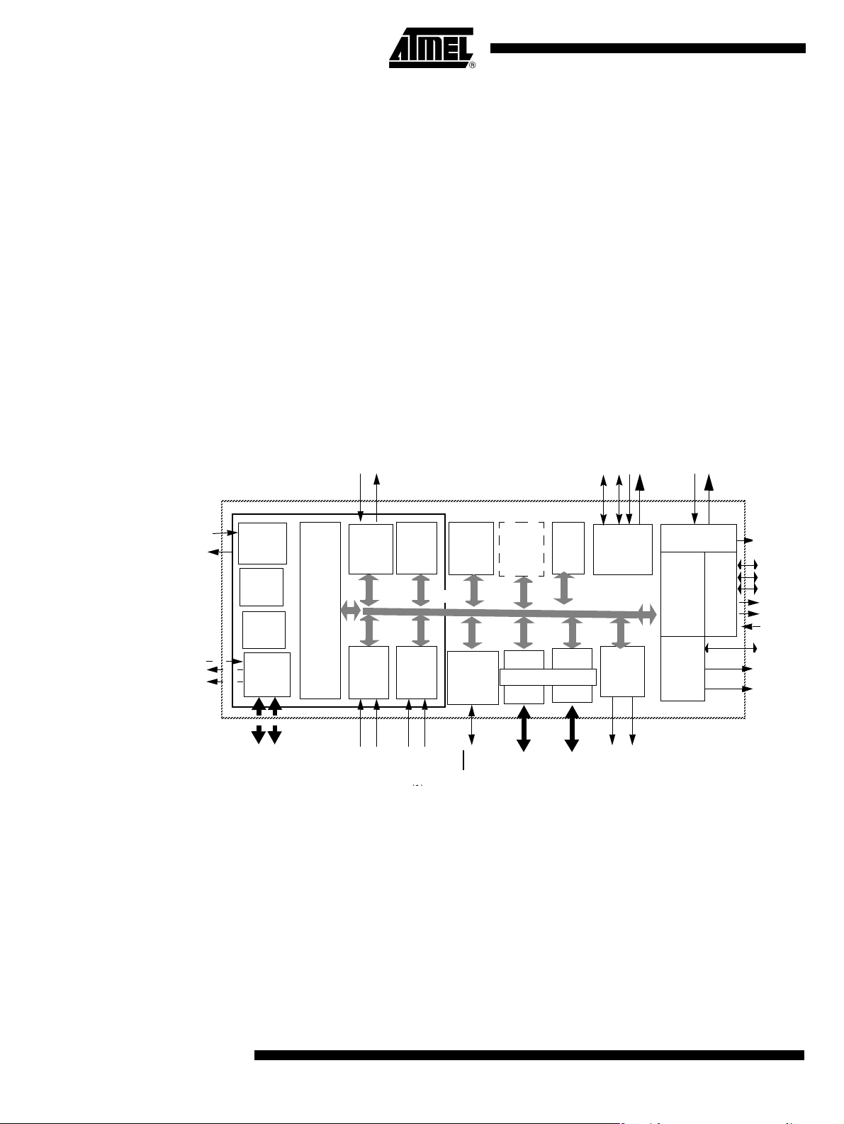
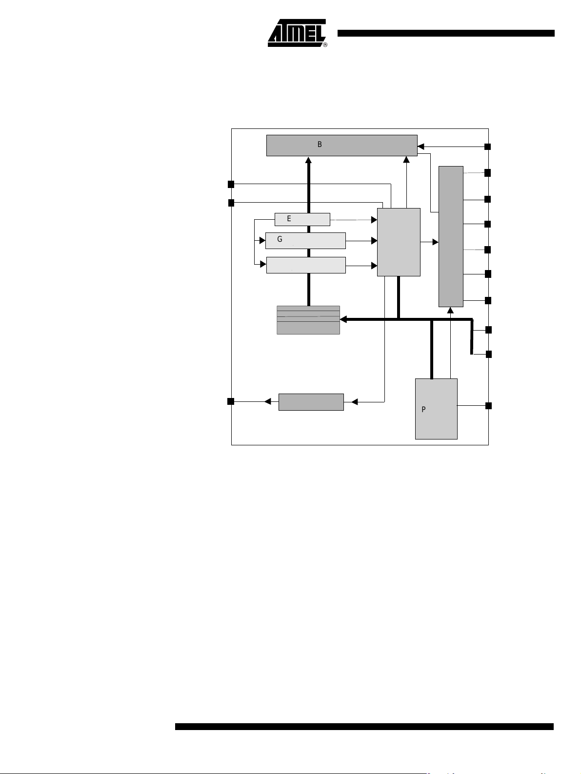
Block Diagram
Figure 1. Block Diagram
CC
CC
CC
V
DV
EV
VSS
LI
CVSS
(2) (2)
RxD
TxD
XTAL1
XTAL2
EA
PSEN
ALE
Xtal
Osc
:1-16
Clock
Prescaler
X2
(4)
P0
P2
CPU
EUART
BRG
Timer 0
Timer 1
(2)(2) (2)(2)
RAM
256 x8
C51
CORE
INT
Ctrl
T0
T1
INT1
INT0
Notes: 1. Alternate function of Port 1
2. Alternate function of Port 3
3. Only for the Code RAM version
4. Only for PLCC52
ROM
16K x8
IB-bus
Watchdog
POR
PFD
RST
(3)
CRAM
16K x8
6 I/Os
XRAM
256
x8
8 I/Os
Parallel I/O Ports
P1
P3
Voltage
Direct
Output
(2)
Reg.
Drive
LED
(2)
LED0
LED1
DC/DC
Converter
SCIB
Alternate
Card
Level
Shifters
(1)
(1)
(1)
(1)
(1)
(1)
CPRES
(2)
(2)
CRST1
(2)
CCLK1
CV
CC4
CC8
CIO
CRST
CCLK
CIO1
CC
2
4164G–SCR–07/06
Page 3
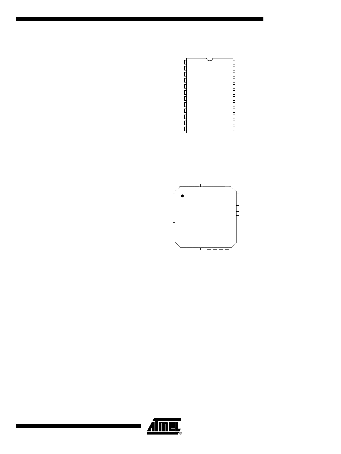
Pin Description Figure 2. 24-pin SSOP Pinout
A/T8xC5121
P1.5/CRST
P1.4/CCLK
P1.2/CPRES
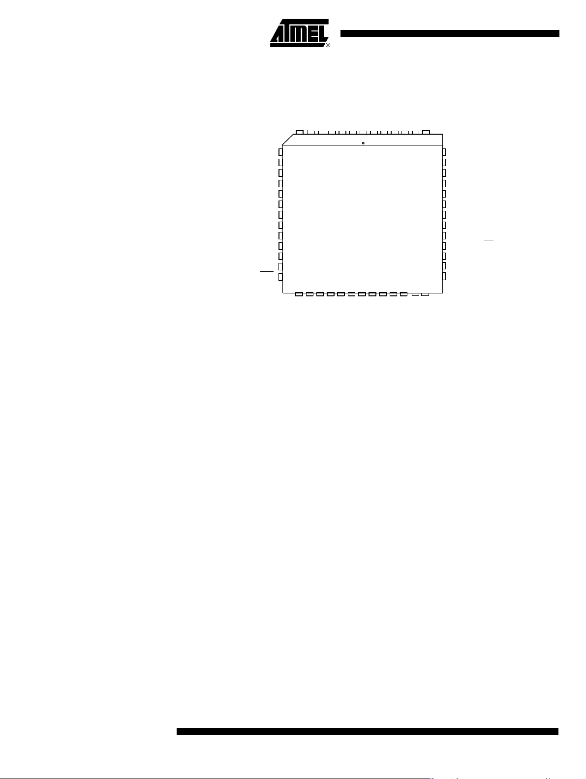
Figure 3. QFN32 Pinout
CVcc
P1.5/CRST
P1.4/CCLK
P1.3/CC4
P1.2/CPRES
P1.1/CC8
P1.0/CIO
CVSS
V
C
P1.3/CC4
P1.1/CC8
P1.0/CIO
RST
XTAL2
XTAL1
RST
1
LI
2
3
CC
4
5
6
7
8
9
10
11
12
N/C
CVss
LI
N/C
28 27 26
1
2
3
4
5
QFN32
6
7
8
1211109131415
24
V
CC
23
EVCC
22
D
V
CC
21
VSS
P3.0/RxD
20
P3.1/TxD
19
P3.3/INT1/OE
18
P3.4/T0
17
P3.2/INT0
16
P3.5/CIO1/T1
15
14
P3.6/CCLK1/LED0
P3.7/CRST1/LED1
13
Vcc
EVcc
N/C
DVcc
2529303132
Vss
24
Vss
23
P3.0/RxD
22
P3.1/TxD
21
P3.3/INT1/OE
20
P3.4/T0
19
P3.2/INT0
18
P3.5/CIO1/T1
17
16
N/C
N/C
N/C
XTAL2
XTAL1
P3.7/CRST1/LED1
N/C
P3.6/CCLK1/LED0
4164G–SCR–07/06
3
Page 4
A/T8xC5121
Figure 4. PLCC52 Pinout
P1.4/CCLK
P1.3/CC4
EA
PSEN
ALE
P2.7/A15
P2.6/A14
P2.5/A13
P1.2/CPRES
P1.1/CC8
P1.0/CIO
P2.4/A12
RST
10
11
12
16
17
18
19
20
8
9
13
14
15
CC
V
NC
NC
C
P1.5/CRST
5 4 3 2 1 6
7
CVSS
LI
CC
NC
V
52 51 50 49 48
2122 26252423 292827 30 31
CC
VSS
V
XTAL1
XTAL2
P0.5/AD5
P2.1/A9
P2.3/A11
P2.2/A10
CC
V
E
P2.0/A8
NCNCNC
32 33
P0.7/AD7
P3.7/CRST1/LED1
NC
47
46
D
V
45
44
43
42
41
40
39
38
37
36
35
34
P0.4/AD4
P3.6/CCLK1/LED0
CC
VSS
P3.0/RxD
P3.1/TxD
P0.0/AD0
P0.1/AD1
P0.2/AD2
P0.3/AD3
P0.6/AD6
P3.3/INT1/OE
P3.4/T0
P3.2/INT0
P3.5/CIO1/T1
4
4164G–SCR–07/06
Page 5

Signals All the T8xC5121 signals are detailed in Table 1.
The port structure is described in Section “Port Structure Description”.
Table 1. Ports Description
Internal
Power
Supply ESD Type Description
Port
Signal
Name Alternate
A/T8xC5121
P1.0 CIO CV
P1.1 CC8 CV
P1.2 CPRES V
P1.3 CC4 CV
CC
CC
CC
CC
4 kV I/O
I/O
4 kV O
O
4 kV I
I/O
4 kV O
Smart ca rd interf ace function
Card I/O.
Input/Out p ut func tion
P1.0 is a bi-directional I/O port .
Reset co nfiguration
I
Input .
Smart ca rd interf ace function
Card contact 8
Output function
P1.1 is a Push-pull port.
Reset co nfiguration
I
Input
Smart ca rd interf ace function
Card presence
Input/Out p ut func tion
P1.2 is a bi-directional I/O port with internal pull-ups- ( External Pull-up
configuration can be selected).
Reset co nfiguration
I
Input (high leve l due to internal pu ll-up)
Smart ca rd interf ace function
Card contact 4
P1.4 CCLK CV
P1.5 CRST CV
4164G–SCR–07/06
CC
CC
4 kV O
I/O
4 kV O
I/O
Output function
O
P1.3 is a Push-pull port.
Reset co nfiguration
I
Input (high leve l due to internal pu ll-up)
Smart ca rd interf ace function
Card clock
Input/Out p ut func tion
P1.4 is a a Push-pull port.
Reset co nfiguration
O
Output at low level
Smart ca rd interf ace function
Card reset
Input/Out p ut func tion
P1.5 is a a Push-pull port.
Reset co nfiguration
O
Output at low level
5
Page 6

A/T8xC5121
Table 1. Ports Description (Continued)
Internal
Power
Supply ESD Type Description
Port
Signal
Name Alternate
P3.0 RxD EV
P3.1 TxD EV
P3.2 INT0 DV
CC
CC
CC
UART function
I
Receive data input
Input/Out p ut func tion
I/O
P3.0 is a bi-directional I/O port with internal pull-ups.
Reset co nfiguration
I
Input ( high level)
UART function
O
Transmit data output
OE active at low or high level depending of PMSO EN bits in SIOCON Reg.
Input/Out p ut func tion
I/O
P3.1 is a bi-directional I/O port with internal pull-ups.
Reset co nfiguration
Z
High impedance due to PMOS switched OFF
External interrupt 0
input set IE0 in the TCON register. If bit IT0 in this register is set, bits IE0
INT0
I
are set by a falling edge on INT
level on INT0
Input/Out p ut func tion
I/O
P3.2 is a bi-directional I/O port with internal pull-ups.
Timer 0: Gate input
I
INT0 serves as external run control for Timer 0 when
select ed in TCON register.
.
0. If bit IT0 is cleared, bits IE0 is set by a low
P3.3 INT1 OE EV
P3.4 T0 EV
Reset co nfiguration
I
Input ( high level)
External Interrupt 1
INT1
CC
CC
I
I
I/O
I
I
O
input set OEIT in ISEL Register, IE1 in the TCON register.
If bit IT1 in this register is set, bits OEIT and IE1 are set by a falling edge on
. If bit IT1 is cleared, bits OEIT and IE1 is set by a low level on INT1
INT1
UART function
Output enable. A low or high level (depending OELEV bit in
ISEL Register) on this pin disables the PMOS transistors of TxD
(P3.1) and T0 (P3.4). This function can be disabled by sof tware
Input/Out p ut func tion
P3.3 is a bi-directional I/O port with internal pull-ups.
Timer 1 function: Gate input
INT1 serves as external run control for Timer 1 when
select ed in TCON register.
Reset co nfiguration
Input ( high level)
UART function
OE active at low or high level depending of PMSOEN
bits in SIOCON Reg.
6
4164G–SCR–07/06
Page 7

Table 1. Ports Description (Continued)
Internal
Signal
Port
P3.5 CIO1 DV
Name Alternate
Power
Supply ESD Type Description
CC
Input/Out p ut func tion
I/O
P3.4 is a bi-directional I/O port with internal pull-ups.
Timer 0 function: External clock input
I
When Timer 0 operates as a counter, a falling edge on the T0 pin
increments the count.
Reset co nfiguration
Z
High impedance due to PMOS switched OFF
Alternate card function
I/O
Card I/O
Input/Out p ut func tion
I/O
P3.5 is a bi-directional I/O port with internal pull-ups.
Timer 1 function: External clock input
I
When Timer 1 operates as a counter, a falling edge on the T1 pin
increments the count.
A/T8xC5121
P3.6 CCLK1 LED0 DV
P3.7 CRST1 DV
P3.7 CRST1 LED1 DV
CC
CC
CC
Reset co nfiguration
I
Input (high leve l due to internal pu ll-up)
Alternate card function
O
Card clock
LED function
Thes e pin s ca n be directly connecte d to t h e cat hode of standa r d
O
LED without external current limitin g resistor s. The typical current
of each output can be programmed by software to 2, 4 or 10 mA
(LEDCON register).
Input/Out p ut func tion
I/O
P3.6 is a LED port.
Reset co nfiguration
I
Input at high level
Alternate card function
O
Card reset
O LED function
Thes e pin s ca n be directly connecte d to t h e cat hode of standa r d
LED without external current limitin g resistor s. The typical current
of each output can be programmed by software to 2, 4 or 10 mA
(LEDCON register).
I/O Input/Out p ut func tion
P3.7 is a a LED port.
4164G–SCR–07/06
I Reset configuration
Input at high level
7
Page 8

A/T8xC5121
Table 1. Ports Description (Continued)
Internal
Power
Supply ESD Type Description
Port
Signal
Name Alternate
RST V
CC
I/O Reset input
Holding this pin low for 64 oscillator periods while the oscillator
is running reset s the device. The Po rt pins are driven to their reset
cond iti on s w he n a vo ltag e lower than V
not the os cillator is running.
This pin has an internal pull-up resistor which allows the device to be reset by
connecting a capacitor between this pin and VSS.This capacitor is optional
thanks to the internal POR which output a Reset as long as Vcc has not
reached the POR threshold level
Asserting RST
return s the chip to normal op eration.
The output is active for at least 12 oscillator periods when an internal
reset occurs.
XTAL1 V
CC
I Input to the on-chip inverting oscillator amplifier
T o use the internal oscillator, a crystal/resonator circuit is connected
to this pin.
If an external oscillator is used, its output is connec ted to this pin.
XTAL2 V
CC
O Output of the on-chip inverting oscillator amplifier
T o use the internal oscillator, a crystal/resonator circuit is connected
to this pin.
If an external oscillator is used, XTAL2 may be lef t unconnected.
V
CC
PWR Supply voltage
is used to power the internal voltage regulators and internal I/O’s.
V
CC
LI PWR DC/DC input
LI must be tied to V
the curr ent for the pump charge of the DC/DC converter.
is applied, whether or
IL
when the chip is in Idle mode or Power-down mode
through an external coil (typically 4, 7 μH) and provi de
CC
CV
CC
PWR Card Sup ply voltage
is the programmable voltage output for the Card interface.
CV
CC
It must be connected to an external decoupling capacitor.
DV
CC
PWR Digital Sup ply voltage
is used to supply the digital core and internal I/Os. It is
DV
CC
interna ll y co nnect e d to the ou tp ut of a 3V re gul a tor and must be co nn ec ted t o
an exte rn a l de co upling capa ci t o r.
EV
CC
V
CC
PWR Extra supply voltage
is used to supply the level shifters of UART interface I/O
EV
CC
pins. It must be connected to an external decoupling capacitor.
This reference voltage is generated internally (automatically or not),
or it can be connected to an external voltage reference.
CVSS GND DC/DC ground
CVSS is used to sink high shunt currents from the external coil.
VSS GND Ground
8
4164G–SCR–07/06
Page 9

Table 1. Ports Description (Continued)
Internal
Signal
Port
Name Alternate
ONLY FOR PLCC52 version
Power
Supply ESD Type Description
A/T8xC5121
P0[7:0] AD[7:0] V
P2[7:0] A[15:8] V
P3.6 WR DV
P3.7 RD DV
ALE V
PSEN PSEN V
EA EA V
CC
CC
CC
CC
CC
CC
CC
I/O Input/Output function Port 0
P0 is an 8-bit open-drain bi-directional I/O port. Port 0 pins that
have 1s written to them float and can be used as high impedance
inputs. T o avoid any parasitic current consumption, Floating P0
inputs must be pulled to V
CC
or VSS.
I/O Address/Data low
Mutiplexed Address/Data LSB for external access
I/O Input/Output function Port 2
P2 is an 8-bit open-drain bi-directional I/O port with internal pull-ups
O Address high
Address Bus MSB for external access
O Write signal
Write signal asserted during external data memory write operation
I Read signal
Read signal asserted during external data memory read operation
O Address latch enable output
The falling edge of ALE strobes the address into e x ternal latch
O Program strobe en ab le
I External access enable
This pin must be held low to force the device to fetch code from
external progra m memory starting at address 0000h. It is la tched
during reset and cannot be dynamicall y changed during operation.
4164G–SCR–07/06
9
Page 10
A/T8xC5121
Port Structure
The different ports structures are described as follows.
Description
Quasi Bi-directional Output Configuration
Figure 5. Quasi Bi-directional Output Configuration
The default port output configuration for standard I/O ports is the quasi bi-directional output that is comm on on the 80 C5 1 an d mo st o f its de rivati ve s. Thi s o utput ty pe ca n b e
used as both an input and output without the need t o reconfigure the port. This is possible because whe n t he port out puts a l ogic h igh, it i s weak ly driven, al lowing an external
device to p ull th e pi n low . Wh en the po rt o utput s a lo gic l ow s tate , it is driv en s trongl y
and able to sink a fai rly large current . These fe atures are so mewhat sim ilar to an ope n
drain output except that there are three pull-up transistors in the quasi bi-directional output that serve different purposes. One of these pull-ups, called the weak pull-up, is
turned o n wheneve r the po rt latch for the pin contains a logic 1. The weak pull-up
sources a very sm all current th at will pull the pin high if it is left floating . A secon d pullup, called the medium pull-up, is turned on when the port latch for the pin contains a
logic 1 and the pin itself is also at a logic 1 level. This pull-u p provides the primary
source current for a quasi bi-directional pin that is outputting a 1. If a pin that has a logic
1 on it is pull ed low by a n ex ternal d evice , the m edi um pul l-up tu rns off, and only the
weak pull-up remains on. In order to pull the pin low under these conditions, the external
device has to sink enough current to overpower the medium pull-up and take the voltage
on the port pin below its input threshold.
2 CPU
CLOCK DELAY
PMOS
P
Strong
P
Weak
P
Medium
Port latch
Data
Push-pull Out p ut Configuration
Pin
N
NMOS
Input
Data
The Push-pull output configuration has the same pull-down structure as the quasi bidirection al outp ut mod es, bu t prov ide s a cont inuou s strong pull- up w hen the p ort la tch
contains a l ogic 1. The P ush-pull mod e may be use d when more source curre nt is
needed from a port output. The Push-pull port configuration is shown in Figure 5.
10
4164G–SCR–07/06
Page 11
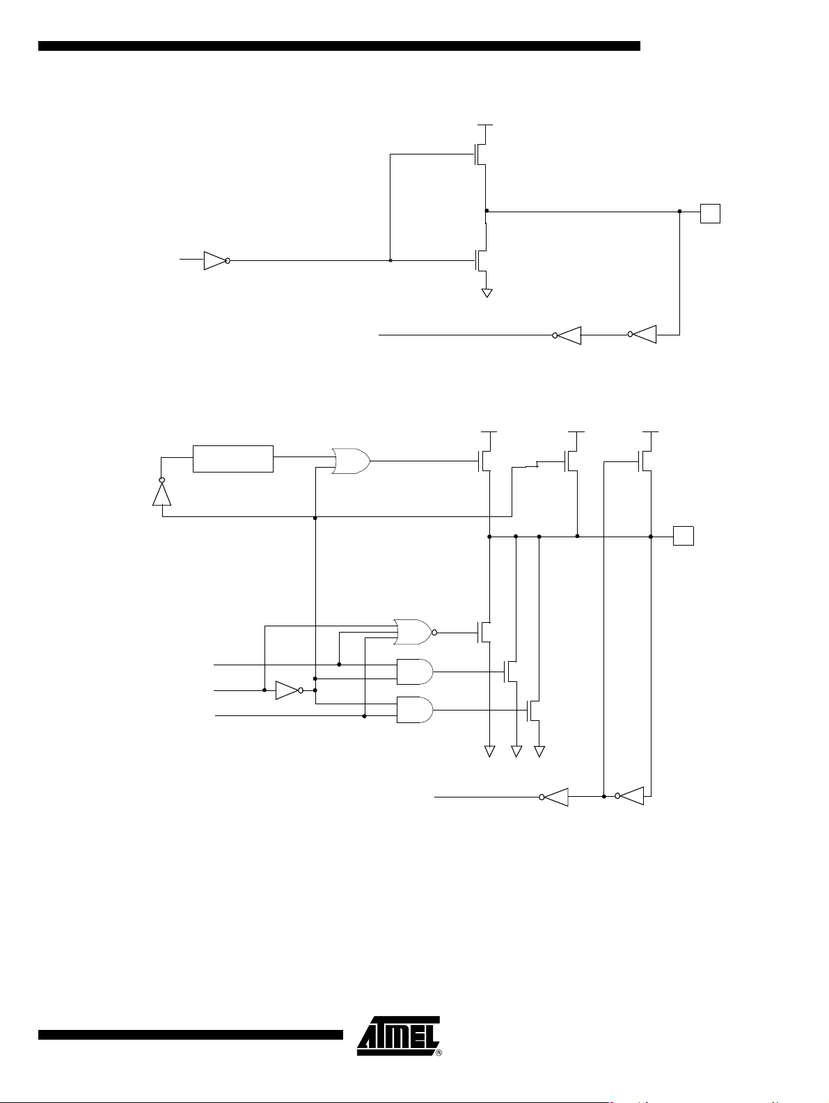
Figure 6. Push-pull Output Configuration
PMOS
A/T8xC5121
P
Strong
Port latch
Data
N
NMOS
Input
Data
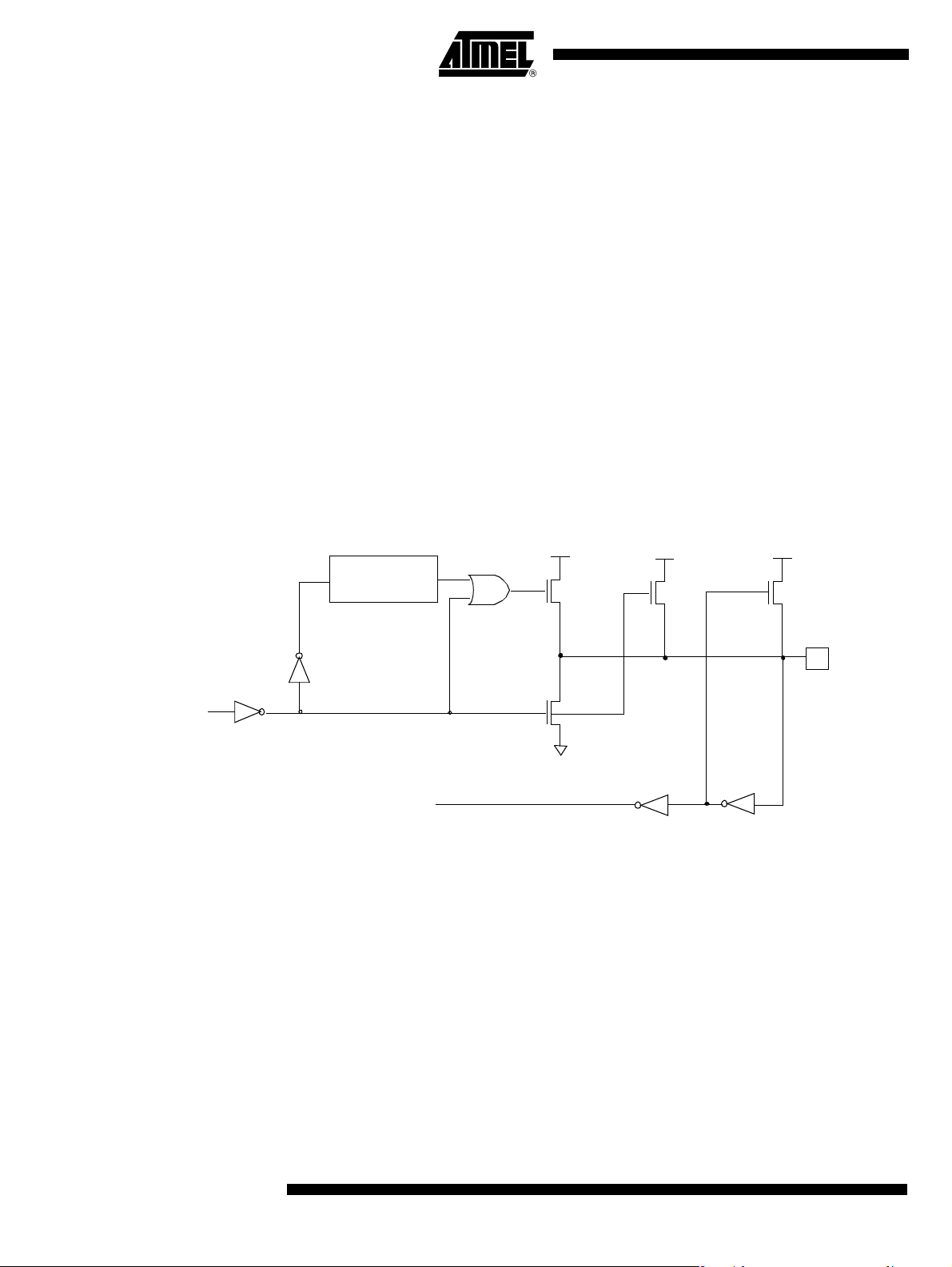
LED Output C on f ig urat i on The input only configuration is shown in Figure 7. Figure 7. LED Source Current Configuration
2 CPU
CLOCK DELAY
PMOS
NMOS
P
Strong
N
P
Weak
Pin
P
Medium
Pin
LEDx.0
Port Latch
Data
LEDx.1
Input
Data
Note: The port can be configured in quasi bi-directional mode and the level of current can be programmed by means of LEDCON0
and LEDCON1 registe rs before switching the led on by writing a logical 0 in Port latch.
LED1CTRL
LED2CTRL
N
N
11
4164G–SCR–07/06
Page 12

A/T8xC5121
SFR Mapping The Special Function Registers (SFR) of the T8xC5121 belongs to the following
categories:
• C51 core registers: ACC, B, DPH, DPL, PSW, SP
• I/O port registers: P0, P1, P2, P3
• Timer 0 registers: TCON, TH0, TH1, TMOD, TL0, TL1
• Serial I/O port registers: SADDR, SADEN, SBUF, SCON, BRL, BDRCON
• Power and clock control registers: PCON, CKRL, CKCON0, CKCON1, DCCKPS
• Interrupt system registers: IE0, IPL0, IPH0, IE1,IPL1, IPH1, ISEL
• Watchdog Timer 0: WDTRST, WDTPRG
• Others: AUXR, AUXR1, RCON
• Smart Card Interface: SCSR, SCC O N/ SCETU0, SCISR/SCETU1, SCIER/SCIIR,
SCTBUF/SCRBUF, SCGT0/SCWT0, SCGT1/SCWT1, SCICR/SCWT2
• Port configuration: SIOCON, LEDCON
12
4164G–SCR–07/06
Page 13
Table 2. SFR Addresses and Reset Values
0/8 1/9 2/A 3/B 4/C 5/D 6/E 7/F
A/T8xC5121
F8h
F0h B
0000 0000
E8h
E0h ACC
0000 0000
D8h
D0h PSW
0000 0000
C8h
C0h
B8h IPL0
XXX0 0000
B0h
A8h
P3
1111 1111
IE0
0XX0 0000
LEDCON
XXXX 0000
RCON
XXXX OXXX
SADEN
0000 0000
IE1
XXXX 0XXX
SADDR
0000 0000
ISEL
0000 0100
IPL1
XXXX 0XXX
SCTBUF*
0000 0000 SCS R
SCRBUF
0000 000
IPH1
XXXX 0XXX
XXX0 1000
0SCWT0 *
1000 0000
1SCGT0 *
0000 1100
0 SCCON *
0X000
1SCETU0
0111 0100
0SCWT1 *
0010 0101
1SCGT1*
0000 0000
0 SCISR*
10X0 0000
1SCETU1
0XXX
0SCWT2 *
0000 0000 IPH0
1 SCICR *
0000 0000
0 SCIIR*
0X00 0000 CKCON1
1SCIER *
0X00 0000
DCCKPS
XXXX XX11
XXX0 0000
XXXX 0XXX
FFh
F7h
EFh
E7h
DFh
D7h
CFh
C7h
BFh
B7h
AFh
A0h P2
1111 1111
98h SCON
XXX0 0000
90h P1
XX11 1111
88h TCON
0000 0000
80h P0
1111 1111SP0000 0111
0/8 1/9 2/A 3/B 4/C 5/D 6/E 7/F
Reserved
4164G–SCR–07/06
SBUF
XXXX XXXX
SIOCON
00XX 0000
TMOD
0000 0000
AUXR1
XXX XXX0
BRL
0000 0000
TL0
0000 0000
DPL
0000 0000
WDTRST
XXXX XXXX
BDRCON
XXX0 0000
TL1
0000 0000
DPH
0000 0000
SCRS Bit (SCSR.0) (*)
0SFR value
1SFR value
TH0
0000 0000
20 PCON
TH1
0000 0000
AUXR
00XX XX00
WDTPRG
XXXX X0000
CKRL
XXXX 111X
CKCON0
X0X0 X000
00XX XX00
A7h
9Fh
97h
8Fh
87h
13
Page 14
A/T8xC5121
PowerMonitor The Powe rMonito r functi on superv ises t he evol ution of the vo ltages f eedin g the mi cro-
controller, and if needed, suspends its activity when the detected value is out of
specification.
It is guaranteed to start up pr operly whe n T8xC512 1 is po wered up and prevents cod e
execution errors when the power supply becomes lower than the functional threshold.
This section describes the functions of the PowerMonitor.
Description In order to start up and to properly maintain the microcontroller operation, V
stabilized in the V
nal amplitude compatible with logic threshold.
This control is carried out during three phases which are the power-up, normal operation
and stop. It complies with the following requirements:
• It guarantees an operational Reset when the microcontroller is powered
• and a protection if the power supply goes out from the functional range of the
Figure 8. PowerMonitor Block Diagram
External
Power Supply
V
DD
microcontroller.
operating range and the oscillator has to be stabilised with a nom i-
DD
DC to DC
3V Regulator
C
V
CC
D
V
CC
has to be
DD
Power-up
Detector
Power-fail
Detector
Internal RESET
PowerMonitor Diagram The target of the PowerMonitor is to survey the power supply in order to detect any volt-
age drops which are not in the target specification. This PowerMonitor block checks two
kind of situations that occur:
• During the power-up condition, when V
• During a steady-state condition, when V
undesirable voltage drops.
Figure 9 shows some configurations that can be met by the PowerMonitor.
14
is reaching the product specification
DD
is stable but disturbed by any
DD
4164G–SCR–07/06
Page 15
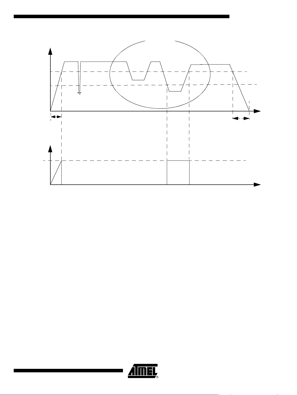
Figure 9. Power-Up and Steady-state Conditions Monitored
DV
CC
VPFDP
VPFDM
A/T8xC5121
Reset
V
CC
t
G
Power-up
t
rise t
Steady-state Condition
Power-down
Such device when it is integrated in a microcontroller, forces the CPU in reset mode
when V
reaches a voltage condition which is out of the specification.
DD
The thresholds and their functions are:
•V
: the output voltage of the regulator has reached a minimum functional value
PFDP
at the power-up . The circuit leaves the RESET mode.
•V
: the output voltage of the regulator has reached a low threshold functional
PFDM
value for the microcontroller. An internal RESET is set.
fall
4164G–SCR–07/06
Glitch fi lt e r ing prevents th e system from R ESET w hen short duration glitches are carried
on V
The ele ctri cal pa ram eter s V
power supply.
DD
PFDP
, V
PFDM
, t
, t
, tG are speci fied i n th e DC para mete rs
rise
fall
section.
15
Page 16

A/T8xC5121
Power Moni toring and Clock Management
For applications where power consumption is a critical factor, three power modes are
provided:
• Idle mode
• Power-down mode
• Clock Management (X2 feature and Clock Prescaler)
• 3V Regulator Modes (pulsed or not pulsed)
Idle Mode An instruction that sets PCON. 0 causes t he last inst ruction to be exec uted bef ore goi ng
into the Idle mode. In the Idle mode, the internal clock signal is gated off to the CPU, but
not to the interrup t, Time r 0, and Serial Port f unction s. The CPU status is prese rved in
its entirety: the Stack Pointer, Program Counter, Program Status Word, Accumulator
and all other registers maintain their data during Idle. The port pins hold the logical
states they had at the time Idle was activated. ALE and PSEN hold at logic high levels.
There are two ways to terminate th e Idle. Activation of any enabl ed interru pt will cause
PCON.0 to be cleared by hardware, terminating the Idle mode. The interrupt will be s erviced, and following RETI the next instruction to be executed will be the one following
the instruction that put the device into idle.
The flag bit GF0 can be used to give an indication if an interrupt occurred during normal
operation or during a n Idle. For exam ple, an i nstructio n that act ivate s Idle can al so set
one or both fl ag bit s. Whe n Idle is term inated by an interrupt, the interrup t serv ice routine can examine the flag bits.
The other way of terminating the Idle mode is with a hardware reset. Since the clock
oscillator is still running, the hardware reset needs to be held active for only two
machine cycles (24 oscillator p er iods) to co mplete the reset.
Power-down Mode
Entering Power-down Mod e To save maximum power, a Power-down mode can be invoked by software (refer to
Table 3, PCON register).
In Power-down mode, the os cillator is stopped a nd the instructi on tha t invoked P ower-
down mode is the last instruction executed. The internal RAM and SFRs retain their
V
value until the Power-down mode is terminated.
power. Eith er a ha rdwa re reset o r an exte rnal interru pt ca n ca use an e xit fro m Powe rdown. To pr operly terminat e Pow er-down, t he reset or ext ernal interr upt sho uld no t be
exec uted befo re
long enough for the oscillator to resta rt and stabi liz e.
Only external interrupts INT0
interrupt must be enabled and configured as level or edge sensitive interrupt input.
Holding the pin low restarts the oscillator but bringing the pi n high com pl etes the exit as
detailed in F igure 10. W hen both interrupt s are ena bled, the oscilla tor restart s as soon
as one of the two inputs is held low and Power-Down exit will be completed when the
first input will be released. In this case the higher priority interrupt service routine is
executed.
Once the in ter rupt is serv iced, the nex t instr uctio n to be e xec uted after RE TI will b e the
one following the instruction that put it into Power-down mode.
Exit from Power-down Mode Exiting from Power-down by external interrupt does not affect the SFRs and the internal
RAM content.
V
is restored to its normal operating level and must be held active
CC
and INT1 are useful to exit from Power-down. For that,
can be lowered to save further
CC
16
4164G–SCR–07/06
Page 17
The ports status under Power-down is the status which was valid before entering this
mode.
The IN T1 int errup t is a m ul tiple xed i nput (s ee Inte rrupt para grap h) w ith CP RES (Car d
detection) and Rxd (U ART Rx) . So these t hree input s can be us ed to exi t from Pow erdown mode. The configurations which must be set are detailed below:
• Rxd input:
• CPRES input:
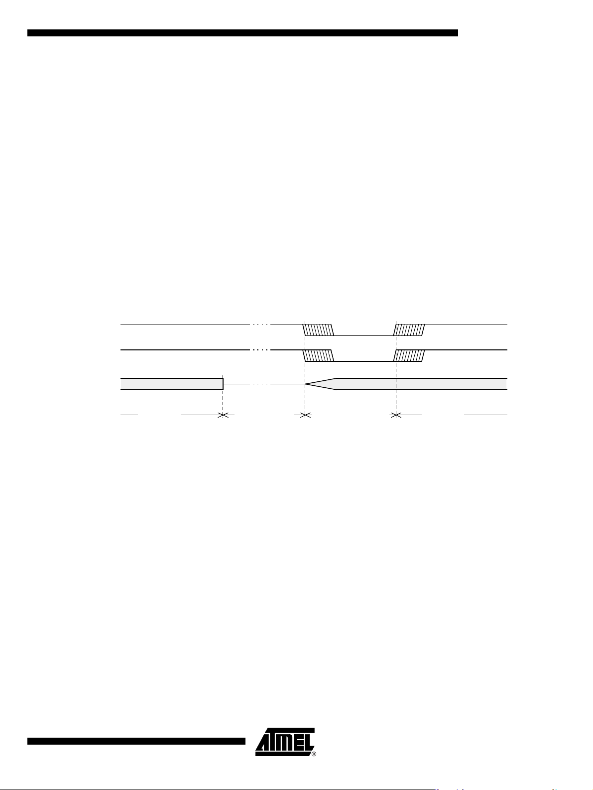
Figure 10. Power-down Exit Waveform
INT0
A/T8xC5121
– RXEN (ISEL.0) must be set
– EX1 (IE0.2) mu st b e set
– A low level detected during more than 100 microseconds exit from Power-
down
– PRSEN (ISEL.1) must be set
– EX1 (IEO.2) must be set
– EA (IE0.7) mu st b e set
– In the INT1 interrupt vector, the CPLEV Bit (ISEL.7) must be inverted
and PRESIT Bit (ISEL.5) must be reset.
INT1
XTAL1
Power-down phase
Oscillator restart phase
Active phaseActive phase
Exiting from Pow er-down by rese t rede fines al l the SF Rs, ex iting from Pow er-down by
external interrupt does no affect the SFRs.
Exiting from Power-down by either reset or external interrupt does not affect the internal
RAM content.
Note: If idle mode is activated wi th Power -down mode (IDL and PD bits set), the exit sequence
is unchanged, when execution is vectored to interrupt, PD and IDL bits are cleared and
idle mode is not entered.
SCI Control Prior to entering Power-down mode, a de-activation of the Smart Card system must be
performed.
LED Control Prior to entering Power-down mode, if the LED mode output is used, the medium pull-up
must be disconnected by setting the LEDPD bit in the PCON Register (PCON 3).
Low Power Mod e Only in Power-down mode, in order to reduce the power consumption, the user can
choose to select this low-power mode.
The activation reference is the following.
• First select the Low-power mode by setting the LP bit in the AUXR Register (AUXR.
6)
• The activation of Power-down can then be done.
4164G–SCR–07/06
17
Page 18

A/T8xC5121
Reduced EMI Mode The ALE signal is used to demultiplex address and data buses on port 0 when used with
external program or data memory. Nevertheless, during internal code execution, ALE
signal is still gene r ated .
Only in case of PLCC52 version, in order to redu ce EMI , ALE s ignal can be disabled by
setting AO bit.
The AO bit is located in AUXR register at b it location 0 (See Table 4). As soon as A O is
set, ALE is no longer output but remains active during MOVX and MOVC instructions
and external fetches. During ALE disabling, ALE pin is weakly pulled high.
Power Modes Control Registers
Table 3. PCON Register
PCON (S:87h)
Power Configuration Register
76543210
SMOD1 SMOD0 - - LEDPD GF0 PD IDL
Bit
Number
7SMOD1
6SMOD0
5 Reserved
4 Reserved
3 LEDPD
2GF0
Bit
Mnemonic Description
Double Baud Rate bit
Set to d ou ble t he Bau d Rat e when Timer 1 i s u sed and mo de 1, 2 o r 3 i s se le cted in
SCON register.
SCON Select bit
When cleared, read/write accesses to SCON.7 are to SM0 bit and rea d/write
accesses to SCON.6 are to SM1 bit.
When set, read/write accesses to SCON.7 are to FE bit and read/write accesses to
SCON.6 are to OVR bit. SCON is Serial Port Control register.
LED Control Power-Down Mode bits
When cleaned the I/O pull-up is the standard C51 pull-up control. When set the
medium pull-up is disconnected.
General-pu r pos e fla g 0
One use is to indi cate wether an interrupt occ urred during normal operation or
during I dl e mo de .
18
Power-down Mode bit
1PD
0IDL
Cleared by hardware when an interrupt or reset occurs.
Set to activate the Power-down mode.
If IDL and PD are both set, PD takes precedence.
Idle Mode bit
Cleared by hardware when an interrupt or reset occurs.
Set to activate the Idle mode.
If IDL and PD are both set, PD takes precedence.
Reset Valu e = X0XX XX 0 0b
4164G–SCR–07/06
Page 19

A/T8xC5121
Table 4. AUXR Register
AUXR (S:8Eh)
Auxiliary Registe r
76543210
- LP - - - - EXTRAM AO
Bit
Number
7-
6LP
5-
4-
3-
2-
1EXTRAM
0AO
Bit
Mnemonic Description
Reserved
The value read from this bit is indeterminate. Do not set this bit.
Low Power mode selection
Clear to select standard mode
Set to select low consumption mode
Reserved
The value read from this bit is indeterminate. Do not set this bit.
Reserved
The value read from this bit is indeterminate. Do not set this bit.
Reserved
The value read from this bit is indeterminate. Do not set this bit.
Reserved
The value read from this bit is indeterminate. Do not set this bit.
EXTRAM select
(ONLY for PLCC52 version)
Clear to map XRAM datas in internal XRAM memory.
Set to map XRAM datas in exter nal XRAM memo ry.
ALE Output bit
(ONLY for PLCC52 version)
Clear to restore ALE operation during internal fetches.
Set to disable ALE operation during internal fetches.
4164G–SCR–07/06
Reset Value = 00XX XX00b
19
Page 20

A/T8xC5121
Table 5. IE0 Register
IE0
Interrupt Enable Register (A8h)
76543210
EA - - ES ET1 EX1 ET0 EX0
Bit
Number
7EA
6-
5-
4ES
3ET1
2EX1
1ET0
Bit
Mnemonic Description
Enable All interrupt bit
Clear to disable all inter rupts.
Set to enab le all in terr u p ts.
If EA = 1, each interrupt source is individually enabled or disabled by setting or
clearing its interrupt enable bit.
Reserved
The value read from this bit is indeterminate. Do not set this bit.
Reserved
The value read from this bit is indeterminate. Do not set this bit.
Serial port Enable bit
Clear to disable serial port interrupt.
Set to enable serial por t int er ru pt.
Timer 1 overflow interrupt Enable bit
Clear to disable Timer 1 overflow interrupt.
Set to enable Timer 1 overflow interrupt.
External interrupt 1 Enable bit
Clear to disable external interrupt 1.
Set to enable external interrupt 1.
Timer 0 overflow interrupt Enable bit
Clear to disable Timer 0 overflow interrupt.
Set to enable Timer 0 overflow interrupt.
20
External interrupt 0 Enable bit
0EX0
Clear to disable external interrupt 0.
Set to enable external interrupt 0.
Reset Value = 0XX0 0000b
4164G–SCR–07/06
Page 21

A/T8xC5121
Table 6. ISEL Register
ISEL (S:BAh)
Interrupt Enable Register
76543210
CPLEV - RXIT PRESIT OELEV OEEN RXEN PRESEN
Bit
Number
7 CPLEV
6-
5 PRESIT
4RXIT
3 OELEV
2OEEN
Bit
Mnemonic Description
Card presence detection level
This bit indicates which CPRES level will bring about an interrupt
Set this bit to indicate that Card Presence IT will appear if CPRES is at high
level.
Clear this bit to indicate that Card Presence IT will appear if CPRES is at low
level.
Reserved
The value read from this bit is indeterminate. Do not set this bit.
Card presence detection interrupt flag
Set by hardware
Must be cleared by software
Received data interrupt flag
Set by hardware
Must be cleared by software
OE/INT1 signal active level
Set this bit to indicate that high level is active.
Clear this bit to indicate that low level is active.
OE/INT1 inte rru pt dis ab le bit
Clear to disable INT1 interrupt
Set to enable INT 1 interr u pt
4164G–SCR–07/06
Card pr es en ce detecti on i nterrupt en able bit
1 PRESEN
0RXEN
Clear to disable the card presence detect ion interrupt comi ng from SCIB.
Set to enable the card pre se nc e detect io n int erru pt com in g from SC IB.
Received data Interrupt enable bit
Clear to disable the RxD interrupt.
Set to enable the RxD in ter r up t
Reset Value = 0X00 0000b
21
Page 22
A/T8xC5121
Clock Management In order to optimize the power consumption and the execution time needed for a specific
task, an internal prescaler feature and a X2 feature have been implemented between
the oscillator and the CPU.
Funct ional Bl ock Diagram
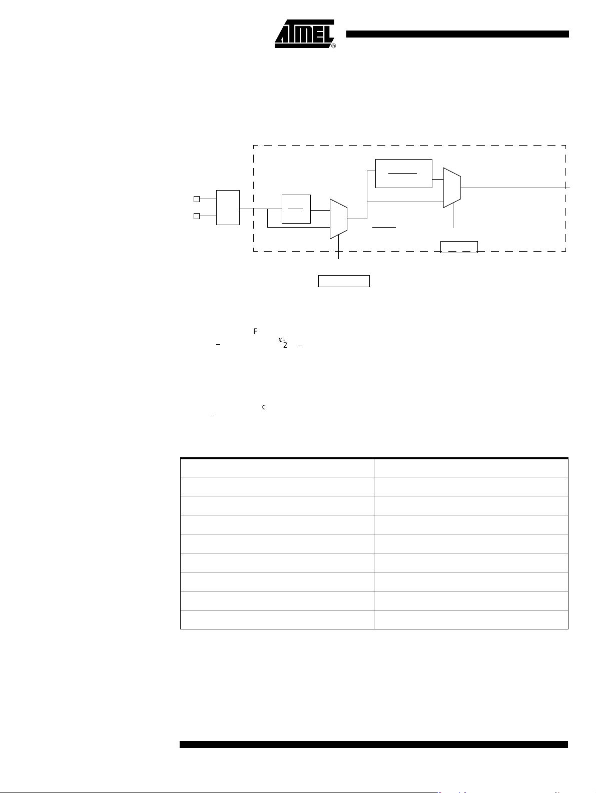
Figure 11 . Clock Generation Diagram
XTAL1
XTAL2
Osc.
F
OSC
1
2
0
1
X2
CKCON0
If CKRL<>7 then:
F
–
CLK CPU
OSC
----- ----------- x2()
2
1
----- ----------- ----------- ------- -=
x
2 7 CKRL
–
()
F
If CKRL = 7 then:
F
–
CLK CPU
Fosc
--------------=
x2
2
2(7-CKRL)
F
OSC
x2
2
1
F
0
1
CKRL = 7
CKRL
CLK_CPU
F
CLK_Periph
22
CKRL Prescalor Factor
71
62
54
46
38
210
112
014
4164G–SCR–07/06
Page 23
A/T8xC5121
X2 Feature The T8xC5121 core needs only 6 clock periods per mach ine cycle. This feature called
”X2” provides the following advantages:
• Divides frequency crystals by 2 (cheaper crystals) while keeping same CPU power.
• Saves power consumption while keeping same CPU power (oscillator power
saving).
• Saves power consumption by dynamical ly dividing the operating frequenc y by 2 in
operating and idle modes.
• Increases CPU power by 2 while keeping same crystal frequency.
In order to keep the original C51 compatibility, a divider by 2 is inserted between the
XTAL1 signal and the main clock input of the core (phase generator). This divider m ay
be disabled by software.
Description The clock for the who le circuit and peripheral s is first divided by tw o before being used
by the CPU core and the peripherals.
This allows any cyclic ratio to be accepted on XTAL1 input. In X2 mode, as this divider is
bypassed, the signals on XTAL1 must have a cyclic ratio from 40 to 60%.
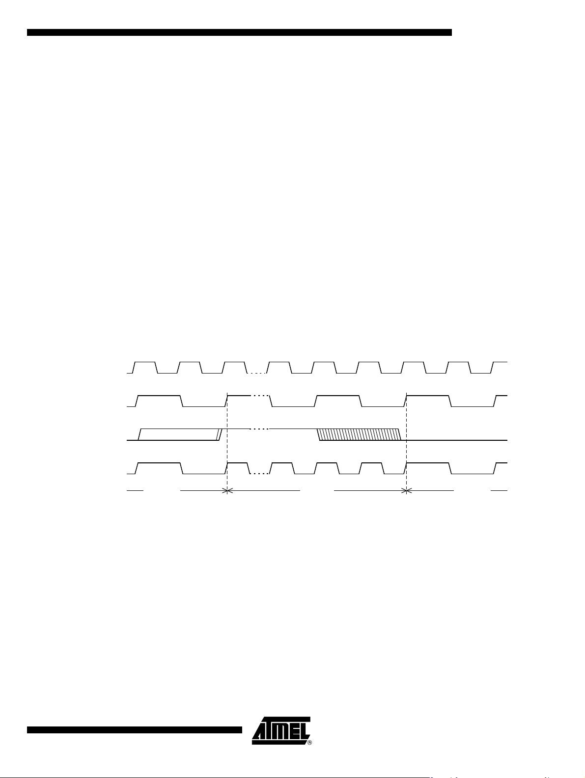
As shown in Figure 11, X2 bit is validated on the rising edge of the XTAL1÷2 to avoid
glitches when switching from X2 to standard mode. Figure 12 shows the switching mode
waveforms.
Figure 12. Mode Switching Waveforms
XTAL1
XTAL1:2
X2 bit
CPU clock
The X2 bit in t he CKCON 0 reg ister (se e Table 9) al lows to s witch (if CK RL=7) from 12
clock periods per instruction to 6 clock periods and vice versa.
The T0X2, T1X2, UartX2, and WdX2 bits in the CKCON0 register (see Table 9) and
SCX2 bit in the CK CON1 registe r (see Tab le 10) allow to s witch f rom standa rd perip heral speed (12 clock periods per peripheral clock cycle) to fast peripheral speed (6 clock
periods per peripheral clock cycle). These bits are active only in X2 mode.
More information about the X2 mod e can be f ound in the application note "How to Take
Advantage of the X2 Features in TS80C51 Microcontroller?".
F
OSC
X2 ModeSTD Mode STD Mode
4164G–SCR–07/06
23
Page 24

A/T8xC5121
Clock Prescaler Before supplying the CPU and the peripherals, the main clock is divided by a factor 2 to
30 to reduce the CPU power consumption. This factor is controlled with the CKRL
register.
Table 7. Examples of Factors
F
XTAL (MHz) X2 CPU CKCON0 CKRL Value Prescaler Factor
16 0 (reset mode) 07h 1 8
16 1 (X2 mode) 07h 1 16
16 1 07h 1 16
16 0 07h 1 8
16 0 06h 2 4
16 1 06h 2 8
Clock Control Registers
Clock Prescaler Register This register is used to reload the clock prescaler of the CPU and peripheral clock.
CLK_CPU, FCLK_Periph
(MHz)
Table 8. CKRL Register
CKRL - Clock Reload Register (97h)
76543210
- - - - CKRL CKRL CKRL -
Bit
Number
7 - 4 -
3 - 1 CKRL
0-
Bit
Mnemonic Description
Reserved
The value read from this bit is indeterminate. Do not set this bit.
Clock Reload Register
Prescaler value
XXXX 000Xb: CKRL=7 and Division factor equals 14
XXXX 110Xb: CKRL=6 and factor equals 2
XXXX 111Xb: CKRL=7 and division fa ctor equal s 1
Reserved
The value read from this bit is indeterminate. Do not set this bit.
Reset Value = XXXX 111Xb
24
4164G–SCR–07/06
Page 25

A/T8xC5121
Table 9. CKCON0 Register
CKCON0 - Clock Control Register (8Fh)
76543210
-WDX2- SIX2 - T1X2T0X2X2
Bit
Number
7-Reserved
6WDX2
5-Reserved
4SIX2
3-Reserved
2T1X2
1T0X2
Bit
Mnemonic Description
Watchdog clock
(This control bit is validated when the CPU clock X2 is set; when X2 is low, this
bit has no effect)
Cleared to select 6 clock periods per per ipheral clock cycle.
Set to select 12 clock periods per peripheral clock cycle.
Enhanced UART clock (Mode 0 and 2)
(This control bit is validated when the CPU clock X2 is set; when X2 is low, this
bit has no effect)
Clear to select 6 clock periods per peripheral clock cycle.
Set to select 12 clock periods per peripheral clock cycle.
Timer 1 clock
(This control bit is validated when the CPU clock X2 is set; when X2 is low, this
bit has no effect)
Clear to select 6 clock periods per peripheral clock cycle.
Set to select 12 clock periods per peripheral clock cycle
Timer 0 clock
(This control bit is validated when the CPU clock X2 is set; when X2 is low, this
bit has no effect)
Clear to select 6 clock periods per peripheral clock cycle.
Set to select 12 clock periods per peripheral clock cycle
4164G–SCR–07/06
CPU clock
Clear to select 12 clock periods per machine cycle (Standard mode) for CPU
0X2
and all the peripherals.
Set to select 6 clock periods per machine cycle (X2 mode) and to enable the
indivi dual peripherals "X2" bits.
Reset Value = X0X0 X000b
25
Page 26

A/T8xC5121
Table 10. CKCON1 Register
CKCON1 - Clock Control Register (AFh)
76543210
----SCX2---
Bit
Number
7-Reserved
6-Reserved
5-Reserved
4-Reserved
3SCX2
2-Reserved
1-Reserved
0-Reserved
Bit
Mnemonic Description
SCIB clock
Clear to select 6 clock periods per peripheral clock cycle.
Set to select 12 clock periods per perip heral clock cycle.
Reset Value = XXXX 0XXXb
26
4164G–SCR–07/06
Page 27
A/T8xC5121
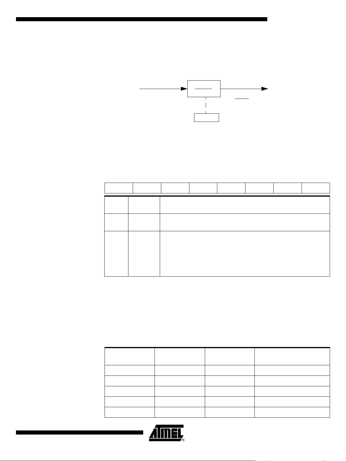
DC/DC Clock The DC/DC block needs a clock with a 50% duty cycle. The frequency must also respect
a value between 3.68 MHz and 4 MHz. The first requirement imposes a divider in the
clock path and the second constraint is solved with the use of a prescaler.
Figure 13. Functional Block Diagram
F
OSC
1
(2 to 5)
DCCKPS
Address BFh
F
OSC
2 to 5
F
CLK_DC/DC
Clock Control Register This register is used to reload the clock prescaler of the DC/DC converter clock.
Table 11. DCCKPS Register
DCCKPS - DC/DC converter Reload Register (BFh)
76543210
- - - - - - DCCKPS DCCKPS
Bit
Number
7:2 -
1:0 DCCKPS
Bit
Mnemonic Description
Reserved
Do not use write those bits
Clock Reload Register
Pres caler value
00b: Divi sion factor equals 2
01b: division factor equals 3
10b: division factor equals 4
1 1b: division factor equals 5 (reset value which minimize the consumption)
Reset Value = XXXX XX11b
Clock Prescaler Before supplying the DC/DC block, the oscillator clock is divided by a factor 2 to 5 to
adapt th e cloc k needed by the DC/DC co nverte r. This factor i s contro lled with t he
DCCKPS register.
The prescaler factor must be chosen to match the requirement range which is 4MHz.
Table 12. Examples of Factors
Prescaler
XTAL (MHz) DCCKPS Value
800h2 4
12 01h 3 4
14.756 02h 4 3.689
16 02h 4 4
20 03h 5 4
4164G–SCR–07/06
Factor DC/DC Converter CLK (MHz)
27
Page 28

A/T8xC5121
28
4164G–SCR–07/06
Page 29

A/T8xC5121
Smart Card Interface Block (SCIB)
Introduction The SCIB provides all signals to directly interface a smart card. Compliance with the
ISO7816, EMV’2000, GSM and WHQL standards has been certified.
Both synchronous (e.g. memory card) and asynchronous smart cards (e.g. micropro-
cessor card) are supported. The component supplies the different voltages requested by
the smart card. The power-off sequence is directly managed by the SCIB.
The card presence switch of the smart card connector is used to detect card insertion or
card removal. In case of card removal, the SCIB de-activates the smart card using the
de-activation sequence. An interrupt can be generated when a card is inserted or
removed.
Any malfunction is reported to the microcontroller (interrupt + control register).
The different operating modes are configured by internal registers.
Main Features • Su pport of ISO/IEC781 6
• Character mode
• 1 transmit buffer + 1 receive buffer
• 11 bits ETU counter
• 9 bits guard time counter
• 24 bits waiting time counter
• Auto-character repetition on error signal detection in transmit mode
• Auto-error signal generation on parity error detection in receive mode
• Power-on and power-off sequence generation
• Manual mode to directly drive the card I/O
4164G–SCR–07/06
29
Page 30
A/T8xC5121
Block Diagram The Smart Card Interface Block diagram is shown in Figure 14.
Figure 14. SCIB Block Diagram
Clk_iso
Clk_cpu
INT
Ba r r e l s h if ter
Etu counter
Guard time
Wa iting t im e
SCI Registers
Interrupt generator
Scart
fsm
I/O
mux
Power on
Power off
fsm
IO (in)
IO (ou t)
CLK
RST
C4 (out)
C8 (out)
CLK1
C4 (in)
C8 (in)
VCARD
Functional Description The architecture of the Smart Card Interface Block is detailed below.
Barrel Shifter It allows the translation between 1 bit serial data and 8 bits parallel data.
The barrel function is useful for character repetition since the character is still present in
the shifter at the end of the character transmission.
This shifter is able to shift the data in both directions and to invert the input or output
value in order to manage both direct and inverse ISO7816-3 convention.
Coupled with the barrel shifter there is a parity checker and generator.
There are 2 regist ers conn ected to this barre l shifter, one for the trans mission and on e
for the reception.
They act as buffers to relieve the CPU of timing constraints.
SCART FSM (Smart Card Asynchronous Receiver Transmitter Finite State Machine)
This is th e c ore of the de sign. I ts pu rpo se is to co ntro l the barre l s hifter. To sequ enc e
correctly the barrel shifter for a reception or a transmission, it uses the signals issued by
30
4164G–SCR–07/06
Page 31

A/T8xC5121
the different counters. One of the most important counters is the guard time counter that
gives time slots corresponding to the character frame.
It is enabled only in UART mode.
The transition from the receipt mode to the transmit mode is done automatically. Priority
is given to the transmission.
ETU Counter The ETU (Elementary Timing Unit) counter controls the working frequency of the barrel
shifter, in fact, it generates the enable signal of the barrel shifter.
It is 11 bits wide and t here i s a special compensation mode activ ated with t he m ost s ig-
nificant bit that allows non integer ETU value with a working clock equal to the card
clock .
But the decimal va lue is limit ed t o a hal f clock cycle. I n fa ct the bit dura ti o n is not fixed. It
takes turns in n clock cycles and n-1 clock cycles. The character duration (10 bits) is
also equal to 10*(n+1/2) clock cycles.
This allows to reach the required precision of the character duration specified by the
ISO7816 standard.
example: F = 372 D = 32 = > ETU = 11.625 clock cycles.
ETU = (ETU[10-0] -0.5 * COMP)*f with ETU[10-0] = 12, COMP = 1 (bit 7 of SCETU1)
To achieve this clock rate we activated the compensation mode and we programmed
the ETU duration to 12 clock cycles.
The result will be a full character duration (10 bits) equal to 11.5 clock cycles.
Guard Time Co unt er The minimum time between the leading edge of the start bit of a character and the lead-
ing edge of the start bit of the following character transmitted (Guard time) is controlled
by one counter.
It is 9 bits wide and is incremented at the ETU rate.
Figure 15. Guard Time Counter
ETU Counter
Guard Time Counter
GT[8:0]
SCGT1 SCGT0
Timeout
4164G–SCR–07/06
31
Page 32

A/T8xC5121
Waiting Time Counter (WT) The WT counter is a 24 bits down counter which can be loaded with the value contained
in the SCW T2, SCW T1, S CWT 0 re gisters . Its m ain p urpos e is tim e ou t sig nal ge neration. It is 24 b its wide an d is decrem ent ed at the ETU rate. The ETU co unter acts as a
prescaler (See Figure 16).
When the WT co unter timeout, an interrupt is gener ated and the SC IB function is
locked: reception and emission are disabled. It can be enabled by resetting the macro or
reloading the counter.
Figure 16. Waiting Time Counter
ETU Counter
WTEN
Write_SCWT2
UART
Start bit
WT Counter
Load
Timeout
WT[23:0]
SCWT2
SCWT1
SCWT0
The counter is loaded, if WTEN = 0, during the write of SCWT2 register.
This counter is available in both UART and m anual mode s. But the behaviour depe nds
on the selected mode.
In manual mode, the WTEN signal controls the start of the counter (rising edge) and the
stop of the count er (falling edge). After a time out of the co unter, a falling edge on
WTEN, a reload of SCWT 2 and a risin g edge of WT EN are neces sary to start aga in the
counter and to release the SCIB macro. The reload of SCWT2 transfers all SCWT0,
SCWT1 and SCWT2 registers to the WT counter.
In UART mode there is an aut oma tic load on the start bit detection. This automatic load
is very useful for changing on-the-fly t he Timeout value since there is a registe r to hold
the load value. This is the case, for example, when in T = 1 a launch is performed on the
BWT Timeout on the start bit of th e last transmitted charac ter. But on the receipt of the
first character an other time out value (CWT) must be used . For this, the new load value
of the waiting time counter must be loaded with CWT before the transmission of the last
character. The reload of SCWT[2-0] with the new value occurs with WTEN = 1.
32
After a time out of the counter in UART mode, the restart is done as in manual mode.
The maximum interv al be tween th e s tart leading edge of a character and the start lead-
ing edge of the next character is loaded in the SCWT2, SCWT1, SCWT0 registers.
In T = 1 mode, the CWT (character waiting time) or the BWT (block waiting time) are
loaded in the same registers.
The maximum time between two consecutive start bit is WT[23:0] * ETU.
When used to check BWT according to ISO 7816, WT can be set between 971 and
15728651.
4164G–SCR–07/06
Page 33

Figure 17. T = 0 Mode
Figure 18. T = 1 Mode
CHAR 1
A/T8xC5121
> GT
CHAR 2
< WT
Reception
BLOC 2
CHAR n+2 CHAR n+3
CHAR 1
< CWT
Transmission
BLOC 1
CHAR 2
CHAR n
< BWT
CHAR n+1
< CWT
Power-on and Power-off FSM In this state, the machine appli es the signals on the smart card in accorda nce with
ISO7816 standard.
To be able to power-on the SCIB, the card presence is mandatory.
Removal of the smart card will automatically start the power-off sequence as described
in Figure 19.
Figure 19. SCI Deactivation Sequence after a Card Extraction
V
CC
RST
4164G–SCR–07/06
CLK
IO
8 Clock Cycles
33
Page 34

A/T8xC5121
Interrupt Gen erator There are several sources of interrup tion but the SCIB m ac ro-cell issues onl y one inter-
rupt signal: SCIB IT.
Figure 20. SCIB Interrupt Sources
Transmit buffer
copied to shift register
Output current
out of range
Output voltage
out of range
Timeout on WT
counter
Complete
transmission
Complete
reception
Parity error
detected
This signal is high l evel ac tive. One of the sources is a ble to set up the interru pt signal
and this is the read of the Smart Card Interrupt register by the CPU that clears this
signal.
ESCTBI
CIccER
ECVccER
SCIB IT
ESCWTI
ESCTI
ESCRI
ESCPI
If during the read of the Smart Card Interrupt register an interrupt occurs, the set of the
corresponding bit into the Smart Card Interrupt register and the set of the interrupt signal
will be delayed after the read access.
Registers There are fourteen registers to control the SCIB macro-cell. They will be described in
the Section “DC/DC Converter”.
Some of the register widths are greater than a byte. Despite the 8 bits access provided
by the BIU, the address mapping of this kind of register respects the following rule:
• The Lowest significant byte register is implemented at the higher address.
This implementation makes access to these registers easier when using high level pro-
gramming language (C,C++).
34
4164G–SCR–07/06
Page 35

A/T8xC5121
Other Features
Clock The Ck-ISO input must be in the range 1 - 5 MHz according to ISO7816.
The ISO Clock diagram and the configuration examples are shown in Figure 20.
Figure 21. Clock Diagram of the SCIB Block
FCLK_CPU
FCLK_Periph
Clk_cpu
SCIB
1
2
SCX2
CKCON 1.3
Reset value = 1
1
Clk_iso
0
F4_8MHz
Table 13. Examples of Settings for Clocks
FCLK Cpu
+ FCL K Periph
Xtal ( MHz) X2 CKCON0
40 2 0 2
4 1 (mode X2) 4 0 4
81 8 1 4
11.05905.529512.7648
( MHz) SCX2
Clk_ iso
(1 to 5 MHz)
14.7456 0 7.3728 1 3.6864
160814
20 0 10 1 5
Alternate Card A second card named "Alternate card" can be controlled.
The Clock signal CCLK1 can be adapted to the XTAL frequency. Thanks to the clock
prescaler which can divide the frequency by 1, 2, 4 or 8. The bits ALTKPS0 and
ALTKPS1 in SCSR Register are used to set this factor.
4164G–SCR–07/06
35
Page 36

A/T8xC5121
Figure 22. Alternate Card
F
CK_IDLE
PR3
1, 2, 4 or 8
F
CK_IDLE
P3.6
V
C
CC
CRST
CIO
CCLK
CPRES
1
0
CCLK1
SIM,SAM
CARD
Main
card
Alternate
card
ALTKPS0,1 SCCLK1
SCSR Reg.
SCSR Reg.
Card Presence Input The internal pull-up on Card Presenc e in put can be disconnected in order to reduce the
consumption (CPRESRES, bit 3 in PMOD0).
V
In this case, an external resistor (typically 1 MΩ) must be externally tied to
CC
.
CPRES input can generate an interrupt (see Interrupt system section).
The detection level can be selected.
SCIB Reset The SCICR register contains a reset bit. If set, this bit generates a reset of the SCI and
its registers. Table 15 shows the SCIB registers that are reseted and their reset values.
Table 14. Reset Values for SCI Registers
Register Name SCIB Reset Value (Binary)
SCICR 0000 0000b
SCCON 0X00 0000b
SCISR 1000 0000b
SCIIR 0X00 0000b
SCIER 0X00 0000b
36
SCSR XXX0 1000b
SCTBUF 0000 0000b
SCRBUF 0000 0000b
SCETU1, SCETU0 XXX X001b, 0111 0100b (372)
SCGT1, SCGT0 XXXX XXX0b, 0000 1100b (12)
SCWT2, SCWT1, SCWT0 0000 0000b, 0010 0101b, 1000 0000b (9600)
4164G–SCR–07/06
Page 37

A/T8xC5121
DC/DC Converter T he Smart Card supply voltage (CV
It is controlled by several registers:
• The register described in Section “SCICR Register” controls the CVCC voltage with
bits CVcc0, CVcc1
• The register described in Section “SCCON Register”, switches ON/OFF the DC/DC
converter with bit CARDV
• After the selection of the card voltage (CVcc[1:0]), the CARVCC bit is used to switch
on the DC\DC converter. The CVccOK bit indicates that the card voltage is within
the voltage range.
• It is mandatory to switch off the CV
CC
) is generated by the integrated DC/DC converter.
CC
before entering in power-down mode.
CC
4164G–SCR–07/06
37
Page 38

A/T8xC5121
Registers Descr ipt ion Table 15. SCICR Register
SCICR (S:B6h, SCRS = 1)
Smart Card Interface Control Register
76543210
RESET CARDDET CVcc1 CVcc0 UART WTEN CREP CONV
Bit Number Bit Mnemonic Description
7 RESET
6CARDDET
5 - 4 CVcc[1:0]
3UART
2WTEN
Reset
Set this bit to reset the SCIB and its configuration
Card presence detector sense
Clear thi s bi t t o i nd icat e t he ca r d pr es en ce det e ctor i s o pened w hen n o c ard
is inserted (CPRES is high).
Set this bit to indicate the card presence detector is closed when no card is
inserted (CPRES is low).
Card Voltage Selection:
CVcc[1] CVcc[0] CVcc
Card UART selection
Clear this bit to use the Card I/O bit to drive the Card I/O pin.
Set this bit to use the Smart Card UART to drive the Card I/O pin.
Also controls the Wait Time Counter as described in Section “Waiting Time
Counter (WT)”
Wa it time counter enab le
Clear this bit t o stop the counter and enable th e load of the Wait Time
counter hold registers.
The hold reg is t e rs ar e load ed with SCWT0, SCWT1 an d S CWT 2 v a lu es
when SCWT2 is written.
Set this bit to start the Wait Time counter. The counters stop when it
reaches the timeout value.
If the UART bit is set, the Wait Time counter automatically reloads with the
hold registers whenever a start bit is sent or received.
000V
0 1 1.8V
10 3V
11 5V
38
1 CREP
0CONV
Reset Value = 0000 0000b
Character repetition
Clear this bit to disable parity error dete ction an d indication on the Card I/O
pin in receive mode and to disable character repetition in transmit mode.
Set this bit to enable parity error indication on the Card I/O pin in receive
mode and to set automatic character repetition when a parity error is
indicated in transmit mode. In receive mode, three times error indication is
performed and the parity error flag is set after four times parity error
detection. In transmit mode, up to three times character repetition is
allowed and the parity error flag is set after five times (reset configuration,
can be set at 4 using CREPSET bit in SCSR Register) consecutive parity
error indication.
ISO convention
Clear this bit to use the direct convention: b0 bit (LSB) is sent first, the
parity bit is added after b7 bit and a low level on the Card I/O pin represents
a “0”.
Set this bit to use the inverse convention: b7 bit (LSB) is sent first, the parity
bit is added after b0 bit and a low level on the Card I/O pin represents a “1”.
4164G–SCR–07/06
Page 39

A/T8xC5121
Table 16. SCCON Register
SCCON (S:ACh, SCRS = 0)
Smart Card Contacts Register
76543210
CLK - CARDC8 CARDC4 CARDIO CARDCLK CARDRST CARDVCC
Bit Number Bit Mnemonic Description
Card Clock Selection
Clear this bit to use the CardClk bit (CARDCLK) to drive Card CLK pin.
7CLK
Set this bit to use XTAL signal to drive the Card CLK pin.
Note: internal synchr onizati on avoids any glitch on the CLK pi n when
switching this bit.
6-
5 CARDC8
4 CARDC4
3 CARDIO
2CARDCLK
1 CARDRST
0 CARDV
Reserved
The value read from this bit is indeterminate. Do not change this bit or write 0.
Card C8
Clear this bit to drive a low level on the Card C8 pin.
Set this bit to set a high level on the Card C8 pin.
Card C4
Clear this bit to drive a low level on the Card C4 pin.
Set this bit to set a high level on the Card C4 pin.
Card I/O
When the UART bit is cleare d in SCICR Reg is te r, the valu e of thi s bit is
driven to the Card I/O pin.
Then this pin can be used as a p s eudo bi-directional I/O when this b it is set.
T o be used as an input, this bit must contain a 1.
Card CLK
When the CLK bit is cleared in SCCON Register, the value of this bit is driven
to the Card CLK pin.
Card RST
Clear this bit to drive a low level on the Card RST pin.
Set this bit to set a high level on the Card RST pin.
Read is not allowed if VCARDOK=0
Card VCC Control
Clear this bit to desactivate the Card interface and set its power-off. The other
bits of SCC regi ster have no effect while this bit is clea red.
CC
Set this bit to power-on the Card interface. The activation sequence shall be
handled by software.
4164G–SCR–07/06
Reset Value = 0X00 0000b
39
Page 40

A/T8xC5121
Table 17. SCISR Register
SCISR (S:ADh, SCRS = 0)
Smart Card UART Interface Status Register
76543210
SCTBE CARDIN CIccOVF CVccOK SCWTO SCTC SCRC SCPE
Bit
Number
7SCTBE
6 CARDIN
5CIccOVF
4CVccOK
3SCWTO
2SCTC
Bit
Mnemonic Description
SCIB transmit buffer empty
This bit is set by hardware when the Transmit Buffer is copied to the transmit shift
register of the S m art Card UA RT.
It is cleared by hardware when SCTBUF is written to.
Card presence status
This bit is set when a card is detected (debouncing filter has to be done in
software).
It is cleared otherwise.
ICC overflow on card
This bit is set when the current on card is above the limit
It shall be cleared by the hardware .
Card voltage status
This bit is set when the output voltage is within the voltage range specified by
CVcc fi eld.
It is cleared otherwise.
Smart card wait Timeout
This bit is set by hardware when the Smart card wait time counter times out.
It shall be cleared by the rel oad of the counter or by the reset of the SCIB.
Smart card transmitted character
This bit is set by hardware when the Smart Card UART has transmitted a
character.
It shall be cleared by software after this register has been read.
40
1SCRC
0SCPE
Smart card received character
This bit is set by hardware when the Smart Card UART has received a character
It is cleared by hardware when SCBUF is read.
Smart card parity error
This bit is set at the same time as SCTI or SCRI if a parity error is detected.
It shall be cleared by software after this register has been read.
Reset Value = 1000 0000b
4164G–SCR–07/06
Page 41

A/T8xC5121
Table 18. SCIIR Register
SCIIR (S:AEh, SCRS = 0)
Smart Card UART Interrupt
Identification Register (read only)
76543210
SCTBI - CIccERR CVccERR SCWTI SCTI SCRI SCPI
Bit
Number Bit Mnemonic Description
SCIB t ransmit buffer interrupt
7SCTBI
This bit is set by hardware when the Transmit Buffer is copied to the transmit
shift register of the Smart Card UART.
It is cleared by hardware when this register is read.
6-
5CIccERR
4 CVccERR
3SCWTI
2SCTI
1SCRI
0SCPI
Reset Value = 0X00 0000b
Reserved
The value read from this bit is indeterminate. Do not change this bit or write 0.
Card current status
This bit is set when the output current goes out of the current range.
It is cleared by hardware when this register is read.
Card v oltage statu s
This b it is set whe n t he o utpu t vol tag e g oe s ou t of t he v olt a ge ra ng e sp eci fie d
by CVcc fi el d.
It is cleared by hardware when this register is read.
Smart card wait Timeout interrupt
This bit is set by hardware when the Smart Card Timer 0 times out.
It is cleared by hardware when this register is read.
Smart card transmit interrupt
This bit is set by hardware when the Smart Card UART completes a
character transmission.
It is cleared by hardware when this register is read.
Smart card receive interrupt
This bit is set by hardware when the Smart Card UART completes a
character recept ion.
It is cleared by hardware when this register is read.
Smart card parity error interrupt
This bit is set at the same time as SCTI or SCRI if a parity error is detected.
It is cleared by hardware when this register is read.
4164G–SCR–07/06
41
Page 42

A/T8xC5121
Table 19. SCIER Register
SCIER (S:AEh, SCRS = 1)
Smart Card UART Interrupt Enable Register
765 4 3210
ESCTBI - CIccER ECVccER ESCWTI ESCTI ESCRI ESCPI
Bit Number
7 ESCTBI
6-
5CIccER
4 ECVccER
3 ESCWTI
2 ESCTI
1 ESCRI
0 ESCPI
Bit
Mnemonic Description
Smart Card UART Transmit Buffer Empty Interrupt Enable
Clear this bit to disable the Smart Card UART Transmit Buffer Empty interrupt.
Set this bit to enable the Smart Card UART Transmit Buffer Empty interrupt.
Reserved
The val ue read from this bi t is indet erminate . Do not change this bit .
Card Current Error Interrupt Enable
Clear this bit to disable the Card Current Error interrupt.
Set this bit to enable the Card Current Error interrupt.
Card Voltage Error Interrupt Enable
Clear this bit to disable the Card Voltage Error interrupt.
Set this bit to enable the Card Voltage Error interrupt.
Smart Card Wait Timeout Interrupt Enable
Clear t his bit to disable th e Smart Card Wait timeout interrupt .
Set this bit to enable the Smart Card Wait timeout interrupt.
Smart Card Transmit Interrupt Enable
Clear this bit to disable the Smart Card UART Transmit interrupt.
Set this bit to enable the Smart Card UART Transmit interrupt.
Smart Card Receive Interrupt Enable
Clear this bit to disable the Smart Card UART Receive interrupt.
Set this bit to enable the Smart Card UART Receive interrupt.
Smart Card Parity Error Interrupt Enable
Clear this bit to disable the Smart Card UART Parity Error interrupt.
Set this bit to enable the Smart Card UART Parity Error interrupt.
42
Reset Value = 0X00 0000b
4164G–SCR–07/06
Page 43

A/T8xC5121
Table 20. SCSR Register
SCSR (S:ABh) Smart Card Selection Register
76543210
- - - CREPSEL ALTKPS1 ALTKPS0 SCCLK1 SCRS
Bit
Number
7-Reserved
6-Reserved
5-Reserved
4 CREPSEL
3-2
1 SCCLK1
0 SCRS
Bit
Mnemonic Description
Character repetition selection
Clear this bit to select 5 times repetition before parity error indication
Set this bit to select 4 times repetition before parity error indication
Alternate Card Clock prescaler factor
ALTKPS1
ALTKPS0
00ALTKPS = 0: prescaler factor equals 1
01ALTKPS = 1: prescaler factor equals 2
10ALTKPS = 2: prescaler factor equals 4 (reset value)
11ALTKPS = 3: prescaler factor equals 8
Alternate card clock selecti o n
Set to select the prescaled clock (CCLK1)
Clear to select the standa rd port configuration (P3.6)
Smart ca r d reg is t e r sel e ction
The SCRS bit selects which set of the SCIB registers is accessed.
Reset Value = XXX0 1000b
Table 21. SCTBUF Register
SCTBUF (S:AA, write-only, SCRS = 0) Smart Card Transmit Buffer Register
76543210
Bit Number Bit Mnemonic Description
––
Can store a new byte to be transmitted on the I/O pin when SCTBE is set.
Bit ordering on the I/O pin depends on the Convention (see SCICR
Register).
Reset Value = 0000 0000b
4164G–SCR–07/06
43
Page 44

A/T8xC5121
Table 22. SCRBUF Register
SCRBUF (S:AA read-only, SCRS = 1)
Smart Card Receive Buffer Register
76543210
––––––––
Bit
Number
––
Bit
Mnemonic Description
Provides the byte received from the I/O pin when SCRI is set.
Bit ord ering on the I/O pin depends on the Convention (see SCICR Regist er).
Reset Value = 0000 0000b
Table 23. SCETU1 Register
SCETU1 (S:ADh, SCRS = 1)
Smart Card ETU Register 1
76543210
COMP
Bit
Number
7COMP
6-3 –
––––ETU10 ETU9 ETU8
Bit
Mnemonic Description
Compensation
Clear this bit when no time compensation is needed (i.e. when the ETU to Card
CLK period ratio is close to an intege r with an error less than 1/4 of Card CLK
period).
Set this bit otherwise and reduce the ETU period by 1 Card CLK cycle for even
bits.
Reserved
The val ue read from these bi ts is indeterminate. Do not change these bits .
44
2-0 ETU[10:8]
ETU MSB
Used together with the ETU LSB (see SCETU0 Register).
Reset Value = 0XXX X001b
4164G–SCR–07/06
Page 45

A/T8xC5121
Table 24. SCETU0 Register
SCETU0 (S:ACh, SCRS = 1)
Smart Card ETU Register 0
76543210
ETU7 ETU6 ETU5 ETU4 ETU3 ETU2 ETU1 ETU0
Bit
Number
7-0 ETU[7:0]
Bit
Mnemonic Description
ETU LSB
The Elementary Time Unit is (ETU[10:0] - 0.5*COMP)/f, where f is the Card CLK
frequency.
According to ISO7816, ETU[10:0] can be set between 11 and 2047.
The default res et value of ETU[10: 0] is 372 (F = 372, D = 1).
Reset Value = 0111 0100b
Table 25. SCGT1 Register
SCGT1 (S:B5h, SCRS = 1)
Smart Card Transmit Guard Time Register 1
76543210
–––––––GT8
Bit
Number
7-1 –
0GT8
Bit
Mnemonic Description
Reserved
The val ue read from these bi ts is indeterminate. Do not change these bits .
T ransmit Gu ard Time MSB
Used together with the Transmit Guard Time LSB (see SCGT0 Register).
4164G–SCR–07/06
Reset Value = XXXX XXX0b
Table 26. SCGT0 Register
SCGT0 (S:B4h, SCRS = 1)
Smart Card Transmit Guard Time Register 0
76543210
GT7GT6GT5GT4GT3GT2GT1GT0
Bit
Number
7-0 GT[7:0]
Bit
Mnemonic Description
T ransmit Guard Time LSB
The minimum time between two consecutive start bits in transmit mode is
GT[8:0] * ETU.
According to ISO 7816, GT can be set between 11 and 266 (11 to 254+12 ETU).
Reset Value = 0000 1100b
45
Page 46

A/T8xC5121
Table 27. SCWT2 Register
SCWT2 (S:B6h, SCRS = 0)
Smart Card Character/Block Wait Time Register 2
76543210
WT23 WT22 WT21 WT20 WT19 WT18 WT17 WT16
Bit
Number
7-0 WT[23:16]
Bit
Mnemonic Description
Wait Time Byte 2
Used together with WT[15:0] (see SCWT0 Register).
Reset Value = 0000 0000b
Table 28. SCWT1 Register
SCWT1 (S:B5h, SCRS = 0) Smart Card Character/Block Wait Time Register 1
76543210
WT15 WT14 WT13 WT12 WT11 WT10 WT9 WT8
Bit
Number
7-0 WT[15:8]
Bit
Mnemonic Description
Wait Time Byte 1
Used together with WT[23:16] and WT[7:0] (see SCWT0 Register).
Reset Value = 0010 0101b
Table 29. SCWT0 Register
SCWT0 (S:B4h, SCRS = 0)
Smart Card Character/Block Wait Time Register 0
46
76543210
WT7 WT6 WT5 WT4 WT3 WT2 WT1 WT0
Bit
Number
7-0 WT[7:0]
Bit
Mnemonic Description
Wait Time Byte 0
WT[23:0] is the reload value of the Wait Time counter WTC.
The WTC is a general-purpose Timer 0. It is using the ETU clock and is
controlled by the WTEN bit (see Section “Waiting Time Counter (WT)”).
When UART bit of SCICR Register is set, the WTC is automatically reloaded at
each start bit of the UART. It is used to check the maximum time between to
consecu tive sta rt bits.
Reset Value = 1000 0000b
4164G–SCR–07/06
Page 47

A/T8xC5121
Interrupt S yst em The T8xC5121 has a total of 6 interrupt vectors: four external interrupts (INT0, INT1/OE,
CPRES, RxD), two Timer 0 interrupts (Timer 0s 0 and 1), serial port interrupt and Smart
Card Interface interrupt. These interrupts are shown in Figure 23.
Figure 23. Interrupt Control System
IPH0, IPL0
High Priority
Interrupt
INT0
0
1
IE0
EX0
3
0
TF0
Rxd
INT1/OE
CPRES
TF1
RI
TI
SCI
1
0
OELEV
0
1
CPLEV
RXEN
OEEN
PRES EN
TCON Reg.
RXIT
0
IE1
1
TCON reg.
IT1
PRESIT
IT0
The selection bits
except IT1 (TCON)
are in ISEL Reg.
Individual
Enable
ET0
EX1
ET1
ES
ESCI
3
0
3
0
0
3
0
IPH1, IPL1
Global
Enable
Interrupt
Polling
Sequence
3
3
0
Low Priority
Interrupt
4164G–SCR–07/06
Each of the interrupt sources can be individually enabled or disabled by setting or clearing a bit in the Interrupt Enable register (see Figure 32). This register also contains a
global disable bit, which must be cleared to disable all interrupts at once.
Each interrupt source can also be individ ually programmed to one of four priority levels
by setting or clearing a bit in the Interrupt Priority register (see Figure 36) and in the
Interrupt Priority High register (see Figure 38). Table 30 shows the bit val ues and priori ty
levels associated with each combination.
Table 30. Priority Level Bit Values
IPH.x IP.x Interrupt Level Priority
0 0 0 (Lowest)
01 1
10 2
1 1 3 (Highest )
47
Page 48

A/T8xC5121
A low-priority interrupt can be interrupted by a high priority interrupt, but not by another
low-priority inte rrupt. A hig h-priori ty interrupt can’t be i nterrupte d by any ot her inte rrupt
source.
If two interrupt requests of different priority levels are receiv ed simultaneously, th e
request of higher priority level is serviced. If interrupt requests of the same priority level
are received simul taneous ly, an in terna l polling sequence determ ines wh ich requ est is
serviced. Thu s within ea ch priority l evel there i s a seco nd priority structure de termine d
by the polling sequence.
Table 31. Interrupt Vector Addresses
Interrupt Source Vector Address
IE0 0003h
TF0 000Bh
IE1 & RxIt & PrIt 0013h
TF1 001Bh
RI & TI 0023h
SCI 0053h
INT1 Interrupt Vector The INT1 interrupt is multiplexed with the three following inputs:
•INT1/OE
• Rxd: Received data on UART
• CPRES: Insertion or removall of the main card
The setting configurations for each input is detailed below:
INT1/OE
Rxd Input A second vector in terrupt i nput is the reception of a cha racter. UA RT Rx in put c an gen-
CPRES Input T he t hird inp ut is the detect ion of a level cha nge on CP RES input (P 1.2). This input can
Input This interrupt input is active under the following conditions:
• It must be enabled thanks to OEEN Bit (ISEL Register)
• It can be active on a level or falling edge: thanks to IT1 Bit (TCON Register)
• If level triggering selection is set, the active level 0 or 1 can be selected with OELEV
Bit (ISEL Register)
The Bit IE1 (TCON Register) is set by hardware when external interrupt detected. It is
cleared when interrupt is processed.
erate an interrupt if enabled with Bit RXEN (ISEL.0). The global enable bits EX1 and EA
must also be set.
Then, the Bi t RXIT (I SEL R egister) i s set by ha rdwa re when a low lev el is dete cted o n
P3.0/RXD input.
generate an interrupt if enabled with PRESEN (ISEL.1), EX1 (IE 0.2) and EA (IE0.7) Bits.
: Standard 8051 interrupt input
48
This detection is done according to the level selected with Bit CPLEV (ISEL.7).
Then the Bit PRESIT (ISEL.5) is set by hardware when the triggering conditions are
met. This Bit must be cleared by software.
4164G–SCR–07/06
Page 49

A/T8xC5121
Table 32. IE0 Register
76543210
EA - - ES ET1 EX1 ET0 EX0
Bit
Number
7EA
6-
5-
4ES
3ET1
2 EX1
1ET0
Bit
Mnemonic Description
Enable All interrupt bit
Clear to di sable all int e r rup t s.
Set to enable al l interrupts.
If EA = 1, each interrupt source is individually enabled or disabled by setting or
clearing its interrupt enable bit.
Reserved
The value read from this bit is indeterminate. Do not set this bit.
Reserved
The value read from this bit is indeterminate. Do not set this bit.
Serial port Enable bit
Clear to disable serial port interrupt.
Set to enable serial port i nterrupt.
Timer 1 overflow interrupt Enable bit
Clear to di sa ble Timer 1 overfl ow in ter rupt.
Set to enable Timer 1 overflow interrupt.
External interrupt 1 Enable bit
Clear to di sable exter n a l int e rr u pt 1.
Set to enable external i nterrupt 1.
Timer 0 overflow interrupt Enable bit
Clear to di sa ble Timer 0 overfl ow in ter rupt.
Set to enable Timer 0 overflow interrupt.
External interrupt 0 Enable bit
0 EX0
Clear to di sable exter n a l int e rr u pt 0.
Set to enable external i nterrupt 0.
Reset Value = 0XX0 0000b
Bit addressable
4164G–SCR–07/06
49
Page 50

A/T8xC5121
Table 33. IE1 Register
76543210
----ESCI---
Bit
Number
7-
6-
5-
4-
3ESCI
2-
1-
0-
Bit
Mnemonic Description
Reserved
The value read from this bit is indeterminate. Do not set this bit.
Reserved
The value read from this bit is indeterminate. Do not set this bit.
Reserved
The value read from this bit is indeterminate. Do not set this bit.
Reserved
The value read from this bit is indeterminate. Do not set this bit.
SCI Interrupt Enable
Clear to disable the SCI interrupt.
Set to enable the SCI interrupt.
Reserved
The value read from this bit is indeterminate. Do not set this bit.
Reserved
The value read from this bit is indeterminate. Do not set this bit.
Reserved
The value read from this bit is indeterminate. Do not set this bit.
Reset Value = XXXX 0XXXb
50
4164G–SCR–07/06
Page 51

A/T8xC5121
Table 34. TCON Register
TCON (S:88h)
Timer 0/Counter Control Register
76543210
TF1 TR1 TF0 TR0 IE1 IT1 IE0 IT0
Bit
Number
7TF1
6TR1
5TF0
4TR0
3IE1
2IT1
1IE0
Bit
Mnemonic Description
Timer 1 Overflow flag
Cleared by the hardware when processor vectors to interrupt routine.
Set by the hardware on Timer 0/Counter overflow when Timer 1 register
overflows.
Timer 1 Run Control bit
Clear to turn off Timer 0/Counter 1.
Set to turn on Timer 0/Counter 1.
Timer 0 Overflow flag
Cleared by the hardware when processor vectors to interrupt routine.
Set by the hardware on Timer 0/Counter overflow when Timer 0 register
overflows.
Timer 0 Run Control bit
Clear to turn off Timer 0/Counter 0.
Set to turn on Timer 0/Counter 0.
Interrupt 1 Edge flag
Cleared by the hardware when interrupt is processed if edge-triggere d (see IT1).
Set by the hardware when external interrupt is detected on the INT
Interrupt 1 Type Control bi t
Clear to select lo w level active (level triggered) for external i nterrupt 1 (INT1).
Set to select falling edge active (edge triggered) for external interrupt 1.
Interrupt 0 Edge flag
Cleared by the hardware when interrupt is processed if edge-triggere d (see IT0).
Set by the hardware when external interrupt is detected on INT
1 pin.
0 pin.
4164G–SCR–07/06
Interrupt 0 Type Control bi t
0IT0
Clear to select lo w level active (level triggered) for external i nterrupt 0 (INT0).
Set to select falling edge active (edge triggered) for external interrupt 0.
Reset Value = 0000 0000b
51
Page 52

A/T8xC5121
Table 35. ISEL Register
76543210
CPLEV OEIT PRESIT RXIT OELEV OEEN PRESEN RXEN
Bit
Number
7 CPLEV
6-
5 PRESIT
4RXIT
3 OELEV
2OEEN
Bit
Mnemonic Description
Card presence detection level
This bit indicates which CPRES level will bring about an interrupt
Set this bit to indicate that Card Presence IT will appear if CPRES is at high
level.
Clear this bit to indicate that Card Presence IT will appear if CPRES is at low
level.
Reserved
The value read from this bit is indeterminate. Do not set this bit.
Card presence detection interrupt flag
Set by hardware
Must be cleared by s oftware
Received data interrupt flag
Set by hardware
Must be cleared by s oftware
OE/INT1 signal active level
Set this bit to indicate that high level is active.
Clear this bit to indicate that low level is active.
OE/INT1 Inte rrupt Disable bit
Clear to disabl e INT1 inte rrup t
Set to enable INT1 interrupt
Card presence detection Interrupt Enable bit
1 PRESEN
0RXEN
Clear to disable the card presence detection interrupt coming from SCIB.
Set to enable the card presence detection interrupt coming from SCIB.
Received data Interrupt Enable bit
Clear to disable the RxD interrupt.
Set to enable the RxD interrupt (a minimal bi t width of 0.1 ms is required to
wake up from Power-Down).
Reset Value = 0000 0100b
52
4164G–SCR–07/06
Page 53

A/T8xC5121
Table 36. IPL0 Register
76543210
- - - PSL PT1L PX1L PT0L PX0L
Bit
Number
7-
6-
5-
4 PSL
3PT1L
2PX1L
1PT0L
0PX0L
Bit
Mnemonic Description
Reserved
The value read from this bit is indeterminate. Do not set this bit.
Reserved
The value read from this bit is indeterminate. Do not set this bit.
Reserved
The value read from this bit is indeterminate. Do not set this bit.
Serial port Priority bit
Refer to PSH for priority level.
Timer 1 overflow inte rr upt Prio rity bit
Refer to PT1H for priority level.
External interrupt 1 Priority bit
Refer to PX1H for priority level.
Timer 0 overflow inte rr upt Prio rity bit
Refer to PT0H for priority level.
External interrupt 0 Priority bit
Refer to PX0H for priority level.
Reset Value = XXX0 0000b
Bit addressable
4164G–SCR–07/06
53
Page 54

A/T8xC5121
Table 37. IPL1 Register
76543210
----PSCIL---
Bit
Number
7-
6-
5-
4-
3 PSCIL
2-
1-
0-
Bit
Mnemonic Description
Reset Value = XXXX 0XXXb
Bit addressable
Reserved
The value read from this bit is indeterminate. Do not set this bit.
Reserved
The value read from this bit is indeterminate. Do not set this bit.
Reserved
The value read from this bit is indeterminate. Do not set this bit.
Reserved
The value read from this bit is indeterminate. Do not set this bit.
Reserved
The value read from this bit is indeterminate. Do not set this bit.
Reserved
The value read from this bit is indeterminate. Do not set this bit.
Reserved
The value read from this bit is indeterminate. Do not set this bit.
Reserved
The value read from this bit is indeterminate. Do not set this bit.
54
4164G–SCR–07/06
Page 55

A/T8xC5121
Table 38. IPH0 Register
76543210
- - - PSH PT1H PX1H PT0H PX0H
Bit
Number
7-
6-
5-
4PSH
3PT1H
2PX1H
Bit
Mnemonic Description
Reserved
The value read from this bit is indeterminate. Do not set this bit.
Reserved
The value read from this bit is indeterminate. Do not set this bit.
Reserved
The value read from this bit is indeterminate. Do not set this bit.
Serial port Priorit y High bit
PSH PS Priority Level
00Lowest
01
10
1 1 Highest
Timer 1 overflow interrupt Priority High bit
PT1H PT1 Priority Level
00Lowest
01
10
1 1 Highest
External interrupt 1 Priority High bit
PX1H PX1 Priority Level
00Lowest
01
10
1 1 Highest
4164G–SCR–07/06
Timer 0 overflow interrupt Priority High bit
PT0H PT0 Priority Level
1PT0H
0PX0H
00Lowest
01
10
1 1 Highest
External interrupt 0 Priority High bit
PX0 HPX0 Priority Level
00Lowest
01
10
1 1 Highest
Reset Value = XXX0 0000b
55
Page 56

A/T8xC5121
Table 39. IPH1 Register
76543210
----PSCIH---
Bit
Number
7-
6-
5-
4-
3 PSCIH
2-
1-
0-
Bit
Mnemonic Description
Reserved
The value read from this bit is indeterminate. Do not set this bit.
Reserved
The value read from this bit is indeterminate. Do not set this bit.
Reserved
The value read from this bit is indeterminate. Do not set this bit.
Reserved
The value read from this bit is indeterminate. Do not set this bit.
SCI Interrupt Priori t y level most significant bit
PSCIH PSCIL Priority le ve l
00Lowest
01
10
1 1 Highest priority
Reserved
The value read from this bit is indeterminate. Do not set this bit.
Reserved
The value read from this bit is indeterminate. Do not set this bit.
Reserved
The value read from this bit is indeterminate. Do not set this bit.
Reset Value = XXXX 0XXXb
56
4164G–SCR–07/06
Page 57

A/T8xC5121
LED Por ts Configuration
The current source of the LED Ports can be adjusted to 3 different values: 2, 4 or 10 mA.
The LED o utpu t is an al terna te fun ction of P3.6 an P3 .7 an d canno t be u sed while the
alternate card function is used.
The control register LEDCON is detailed below.
Registers Definition Table 40. LEDCON Register
76543210
----LED1[1]LED1[0]LED0[1]LED0[0]
Bit
Number
7 - 4 -
3 - 2 LED1[1,0]
1 - 0 LED0[1,0]
Bit
Mnemonic Description
Reserved
The value read from this bit is indeterminate. Do not set this bit.
Port LED1 configuration:
LED1[1] LED1[0] Configuration
0 0 Standard C51 port
0 1 2 mA current source when P3.7 is at Low Level
1 0 4 mA current source when P3.7 is at Low Level
1 1 10 mA current source when P3.7 is at Low Level
Port LED0 configuration:
LED0[1] LED0[0] Configuration
0 0 standard C51 port
0 1 2 mA current source when P3.6 is at Low Level
1 0 4 mA current source when P3.6 is at Low Level
1 1 10 mA current source when P3.6 is at Low Level
Reset Value = XXXX 0000b
4164G–SCR–07/06
57
Page 58

A/T8xC5121
Dual Data Pointer T8xC5121 contains a Dual Data Pointer accelerating data memory block moves. The
Standard 80C52 Data Pointer is a 16-bit value that is used to address off-chip data RAM
or peripherals. In T8xC5121, the standard 16-bit data pointer is called DPTR and
located at SFR location 82H and 83H. The second Data Poin ter name d DPT R1 is
located at the same address than the previous one. The DPTR select bit (DPS / bit0)
chooses the active pointer and it is located into the AUXR1 register. It should be serviced in those sections of code that will periodically be executed within the time required
to prevent a WDT reset.
The user switches between data pointers by toggling the LSB of the AUXR 1. Th e increment (INC) is a solution for this. All DPTR-related instructions use the currently selected
DPTR for any activity. Therefore only one instruction is required to switch from a source
to a destination address . Using the Du al Data Pointer sa ves code an d resources whe n
moves of blocks need to be accomplished.
The second Data Pointer can be used to address the on-chip XRAM.
Table 41. DPL Register
DPL - Low Byte of DPTR1 (82h)
76543210
--------
Reset value = 0000 0000b
Table 42. DPH Register
DPH - High Byte of DPTR1 (83h)
76543210
--------
Reset value = 0000 0000b
58
4164G–SCR–07/06
Page 59

A/T8xC5121
Table 43. AUXR1 Register
AUXR1 - Dual Pointer Selection Register (A2h)
76543210
-------DPS
Bit
Number
7-
6-
5-
4-
3-
2-
1-
0DPS
Bit
Mnemonic Description
Reserved
The value read from this bit is indeterminate. Do not set this bit.
Reserved
The value read from this bit is indeterminate. Do not set this bit.
Reserved
The value read from this bit is indeterminate. Do not set this bit.
Reserved
The value read from this bit is indeterminate. Do not set this bit.
Reserved
The value read from this bit is indeterminate. Do not set this bit.
Reserved
The value read from this bit is indeterminate. Do not set this bit.
Reserved
The value read from this bit is indeterminate. Do not set this bit.
Data pointer 1
Clear to select DPTR0 as Data Poin te r.
Set to select DPTR1 as Data Pointer.
Reset value = XXXX XXX0b
4164G–SCR–07/06
59
Page 60

A/T8xC5121
Memor y Ma na gement
Program Memory All the T8xC 5121 versions implement 16 Kb ytes of ROM memory, 256 Bytes RAM and
256 Bytes XRAM.
The hardware configuration byte and the split of internal memory spaces depends on
the product and is detailed below.
ROM Configuration Byte Table 44. ROM Configuration Byte Hardware Register
76543210
-BLJRB-----
Bit
Number
7 Reserved
6BLJRB
5-0
Bit
Mnemonic Description
Bootloader Jump RAM Bit
Set to co nf ig ur e Us er C od e in R O M
Clear t o configure Bootlader in ROM
Reserved
The BLJRB depends of the product version:
•1: ROM mask version
• 0: EEPROM/CRAM versions
This bit defines if, after reset, either the Customer ROM program or the Bootload er program is executed (for In System programming).
Program ROM Lock Bits The program Lock system protects the on-chip program against software piracy.
The T8xC5121 products are delivered with the highest protection level.
Table 45. T8xC5121 Products Protection Level
Program Lock Bits Protection Description
Security
Level LB1 LB2
60
3PP
P = Programmed
SSOP24 version:
Read function is disable d.But checksum control is sti ll enable d
PLCC52 ve r sion:
MOVC instruction execut ed from ex ternal pro gram memor y are disabled
from fetching code bytes from internal memory ,
is sampled and latched on r es et .
EA
But checksum cont rol is still enabl ed.
External exec ution is po ssible.
4164G–SCR–07/06
Page 61

A/T8xC5121
Memory M apping In the products versions, the following internal spaces are defined:
•RAM
•XRAM
• CRAM: 16 KByt es Program RAM Memo r y
•ROM
The specific accesses from/to these memories are:
• XRAM: if the bit RPS in RCON (described below) is reset, MOVX instructions
address the XRAM space.
• CRAM: if the bit RPS in RCON is set, MOVX instructions address the CRAM
space.
Table 46. RCON Register
76543210
-- RPS
Bit
Number
7-4 -
3RPS
2-0 -
Bit
Mnemonic Description
Reserved
The value read from this bit is indeterminate. Do not set this bit.
CRAM space map bit
Set to map the CRAM spac e dur i ng MO VX ins tructions
Clear to map the Data space during MOVX. This bit has priority over the EXTRAM
bit.
Reserved
The value read from this bit is indeterminate. Do not set this bit.
Reset Value = XXXX 0XXXb
T89C5121 Flash ROM Version Three memory blocks are implemented
• An internal seri al EEPRO M ca n be loaded from external with the application
program.
• The ROM memory contains the Bootloader program. The entry point is located at
address F800h. The lower 14K Bytes between address C000h and F7FFh is, also,
used for the Bootloader program.
• The CRAM is the application program memory. This memory is mapped in the
External RAM space. The bit RPS in RCON (SFR address 0D1h) is set to map the
CRAM space during MOVX instructions
4164G–SCR–07/06
For first programming or an update, the program can be downloaded in the internal
EEPROM (and in the CRAM) from an external device:
• Either an external EEPROM if detected
• or from a host through RS232 serial communication.
For this purpose, an In-System Programming (ISP) is supplied in a Bootloader. This
Bootloader is program masked in ROM space.
The Hardware Byte BLJRB value is 0.
As described on page 7, after Reset, the Bootloader program is executed.
61
Page 62

A/T8xC5121
If a serial communication device (as described above: TWI or RS232) is detected, the
program download its content in the internal EEPROM and in CRAM.
Else, the program is internal ly downloaded from the internal EEPROM into the program
CRAM memory ( 1 6 Kb y tes)
Then, in the two cases, the Boot loader execute s a Long Jump at ad dress 0000h wh ich
initializes the Program counter at the lower address (0000h) of the executable CRAM.
Figure 24. CRAM with ROM and EEPROM Memory Mappings
FFFFh
F800h
C000h
entry point
Bootloader
3FFFh
0000h
T85C121 Code RAM Version Two memory blocks are implemented:
• The ROM memory contains the Bootloader program.
• The CRAM is the Application program memory.
After Reset, the program is downloaded, as described in last paragraph, from either an
external EEPROM or from an host connected on RS232 serial link into the program
CRAM memory of 16 K bytes. Then the Program Counter is set at addres s 0000h of the
CRAM space and the program is executed.
16 Kbytes
256 bytes
CRAM XRAM
256 byte s
RAMROM
62
4164G–SCR–07/06
Page 63

Figure 25. CRAM and ROM Mappings
FFFFh
A/T8xC5121
entry point
Bootloader
3FFFh
0000h
16K bytes
256 byte s
CRAM XRAM
256 byte s
RAMROM
T83C5121 with Mask ROM Version
F800h
C000h
In this version, the customer program is masked in 16 Kbytes ROM.
• The customer program is masked in ROM during the final production phase. The
ROM size will be determined at mask generation process depending of the program
size.
In-System Programming The In-Syst em Progr am ming (ISP ) m ode i s o nly i mplem ent ed i n the fol lowi ng pr oduc t
versions:
• EEPROM version
• CRAM version
(The ROM product version is masked with the customer program and does not need
ISP mode)
The ISP is used to download an Application program in the device and to run it.
The communication protocols which are implemented are: UART and TWI.
Hardware Interface The hardware in relation with the two communication protocols is detailed below:
• TWI protocol
• Serial protocol
4164G–SCR–07/06
63
Page 64

A/T8xC5121
Figure 26. Hardware in Relation with the Two Communication Protocols
DV
CC
DVCC or Ext. VCC (3V)
Optional
Thanks to internal pull-ups
P3.7/CRST1
BOOTLOADER
P3.2/INT0
P2.1
P2.0
UART
TWI
V
CC
TWI
Internal EEPROM
AT24C128
V
CC
V
SS
SDA
SCL
SDA
SCL
Address = 00h
A0 = A1 = 0
wp = 0
(default values if not tied)
EEPROM external
AT24C128
Address = 01h
(A0 = 1,A1 = 0)
DVss Wp = 1
DVCC or Ext.VCC (3V)
ISP Software Tool
EEPROM Mapping The 16K Bytes EEPROM mapping is the following:
0000h
64
3FFD
3FFE
Reserved address
3FFF
The three last bytes are reserved respectively:
• Software Security Byte: address 3FFDh
• CRC Bytes: address 3FFEh and 3FFFh
The use of these bytes is described in the following paragraphs.
Therefore, the User Program must be mapped from 0000h to 3FFCh addres s.
4164G–SCR–07/06
Page 65

A/T8xC5121
Bootloader Functional Diagram
Figure 27. Bootloader Flowchart
Versions:
RAM+ROM RAM+ROM (Pre-prod: Application Program)
RAM,ROM,EEPROM
Bootloader
Execution
SSB & P3.7 test
TWI
ext.bypassed?
bypassed?
ACK?
E2PROM at 01
SSB & P3.6 test
UART bypassed
bypassed?
As described in Section “ROM Configuration Byte”, page 60a ROM bit BLJRB (Boot
Loader Jump ROM Bit) defines which product version is. The Bootloader program is
mapped in RO M s pace f rom address C000h up to FFFFh and the entry point is located
at address F800h.
RESET
versions:
ROM
BLJRB = 1
ROM Bit
ROM
F800h
External E2PROM (at 01) is detected
(Prod)
ROM program
Execution
Progra m is downloaded from
External EEPROM into internal
EEPROM and CRAM
and executed.
ROM
0000h
4164G–SCR–07/06
U Character
received on UART
?
Time Elapsed
ACK?
E2PRO M at 00
RD port = Error c ode =
22h
Serial communication is detected thanks to
Autobaud feature (Table52)
Internal E2PROM (at 00) is detected
Error: No TWI or serial device detected
A serial code is sent on RD pin (P3.7)
An ISP Software can be used from
a PC to program the part.
Atmel FLIP software is available
Progra m is downloaded from
internal EEPROM in CRAM and
executed
65
Page 66

A/T8xC5121
In-System Programming Timings
The download from the internal EEPROM to CRAM is executed after 4 seconds when
operating at 12 MHz frequency.
Protection Mechanisms
Transfer Checks In order to verify that the transfers are free of errors, a CRC check is implemented dur-
ing the download of the program in CRAM.
This test is done at the end of the 16K space programming.
As detailed in the next algorithms:
• in ISP mode, if CRC test pass, a character Y is returned before the CRLF
characters else a character Z is retuned.
• in download mode, a serial data AA is sent on P3.7 port and CRAM is not executed.
For this purpose, the user program must include in the two last upper bytes (address
3FFEh and 3F FFh) the CR C of th e previou s bytes (calcu lated from the addre ss 0000 h
to 3FFFDh).
The following frames are examples including the CRC in the two last upper bytes:
Data Bytes
Address: 3FF E ,3FFF
HSB LSB
2 Byt es CRC
• FF 03 C0 21 04 00 00 08 07 02 08 02 2D DB (CRC = 2DDBh)
• FF 03 80 21 02 04 00 0A 03 06 C0 A8 70 01 E3 3D (CRC = E33Dh)
• FF 03 C0 21 02 01 00 10 02 06 00 00 00 00 05 06 00 00 76 55 49 AC (CRC =
49ACh)
The CRC algorithm is the following :
***************************************************************************************************
Uint16 compute_crc (Uint16 W)
{
UcharC;
W&=(Uint16)0x00FF;
for (C=(Uchar)8;C;C--)
{
if ((Uchar)W&(Uchar)1)
{
W>>=1;
W^= (Uint16)0x8408;
}
66
else
W>>=1;
return W;
4164G–SCR–07/06
Page 67

A/T8xC5121
}
void generate_crc_in_frame(void)
{
checksum_tx=(Uint16) FFFFh; /* init of the crc variable */
/* loop which compute for each byte (data_byte) to load */
checksum_tx=compute_crc((Uint16)data_byte^checksum_tx)^(checksum_tx>>8);
/* end of loop */
checksum=~checksum_tx; /* inverts the checksum, so the check will calculate
the CRC of all the datas and */
/* will find a constant value = F0B8
which is the CRC_REF const. of the Bootloader */
write_frame(LOW_BYTE(checksum)); /* writes the LOW_BYTE of the CRC first */
write_frame(HIGH_BYTE(checksum)); /* writes the HIGH_BYTE */
}
***************************************************************************************************
Table 47. Synthesis of Transfer Protection Mechanisms
Source Target Check
MCU CRAM
Intern . EEP MCU This Read oper ation is s ecured by the Write se quence described above
MCU Intern. EEP
Ext. EEP MCU Same as above as data are transferred to EEP INT and then to CRAM
Notes: 1. The transfer of SSB Byte is also secured by CRC as the CRC is computed on all the
16K data.
2. If a Bad transfer has occurred in the Internal EEPROM (CRC is bad), as the CRC
check is fina ll y done at the end of CRAM progr am ming, application program will NOT
be executed after any Reset.
CRC computed during CRAM Write operation: if error an error code is applied
on P3.7 and Code execution by LJMP000 is not done.
Same pro t ec ti on as in first row above beca us e CRA M is wr itt en in sequenc e
after ea ch page pr og r am m in g of EEP
Read/Write Protec tion
Lock Byte In order to protect the content of the internal EEP ROM , a Sof tware Se cu rity Byte (SSB )
defines two security levels:
• level 0: SSB = 0xFF: Write and Read are allowed
• level 1: SSB = 0xFE: Write is disabled
• level 2: SSB = 0xFC: Write and Read are disabled
4164G–SCR–07/06
This SSB Byte is located at address 3FFDh.
When the level 2 is set, the command to set level 1 is disabled. The security levels can
only be increased.
67
Page 68

A/T8xC5121
The only mean to remove the security level 2 is to send a Full Chip Erase command.
Data By te s
SSB
Address
3FFD
Table 48. Synthesis of Security Mechanisms
Source Function Protection
Internal
EEPROM
Internal
EEPROM
CRAM Write
CRAM Read
Write
Read
The first protection level of the SSB Byte IN the internal EEPROM protects
against ISP Wri te command
The second protection level of the SSB Byte IN the internal EEPROM protects
agains t ISP Read commands
The first protection level of the SSB Byte IN the internal EEPROM protects
against ISP Wri te command in CRAM
The second protection level of the SSB Byte IN the CRAM protects against ISP
Read commands
Configuration Bits The Bootloader tests that TWI component s are connected as slave com ponents on the
TWI external bus and later in the algorithm if characters are received on the UART input.
This default configuration can be changed, after a first programming, in order:
– to disable new programming in download mode from external serial
EEPROM to disable ISP programming using UART and
– to avoid any conflict with the target hardware on external TWI bus or UART.
This can be configured with t he t wo hi gher bi ts o f the SSB Byte detailed in the previous
paragraph.
The bit 7 is used to bypass (if 0) the External TWI Acknowledge test.
The bit 6 is used to bypass (if 0) the UART receipt test.
These two bypass modes can be disabled if a level 0 is applied on, respectively, P3.5
and P3.6 pins. This allows to force and use ISP even if the device has been configured
as programmed device.
68
4164G–SCR–07/06
Page 69

A/T8xC5121
Table 49. Valid Softwa r e Securi ty Byte Values
SSB Values Functions
FE No bypass and level 1 security
FC No bypass and level2 security
BF,BE,BC UART bypass and security levels
7F ,7E,7C External TWI bypass and security levels
3F,3E,3C UAR T and Ext. TWI bypass
UART Protocol
Overview The serial protocol used is described below. Physical Laye r The UART is used to transmit information with the following configuration:
• Character: 8-bit data
• Parity: none
• Stop: 1 bit
• Flow control: none
• Baudrate: autobaud is performed by the bootloader to compute the baudrate
chosen by the host.
Datas and Limits As described in Section “Transfer Checks”, the downloaded program include the CRC
values in the last two upper bytes of the 16K bytes space.
An update of a part of the 16K program cannot be done because the CRC value would
have to be updated with a value which depends of the actual value of the rest of the
program.
So the Program function of the PC Software Tool include the individual program commands (with 64 data bytes) from address 0000h to address 3FFFh.
Frame Description The Se rial Protocol is based on the Intel Hex-type records.
Intel Hex records consist of ASCII characters used to represent hexadecimal values and
are summarized below:
Table 50. Intel Hex Type Frame
Record Mark ‘:’ Reclen Load Offset Record Type Data or Info Checksum
1-byte 1-byte = 40h 2-byte 1-byte 64-byte 1-byte
• Record Mark:
– Record Mark is the start of frame. This field must contain’:’.
• Reclen:
– Reclen specifies that the number of bytes of information or data that follow
the Record Type field of the record.
• Load Offset:
– Load Offset specifies the 16-bit starting load offset of the data bytes,
therefore this field is used only for Program Data Record (see Table 51).
4164G–SCR–07/06
69
Page 70

A/T8xC5121
• Record Type:
– Record Type specifies the command type. This field is used to interpret the
remaining information within the frame. The encoding for all the current
record types are described in Table 51.
• Data/Info:
– Data/Info is a 64 bytes length field. It consists of 64 bytes encoded as pairs
of hexadecimal digits. The meaning of data depends on the Record Type.
• Checksum:
– The two’s complement of the 8-bit bytes that result from converting each pair
of ASCII hexadecimal digits to one byte of binary, and including the Reclen
field to and including the last byte of the Data/Info field. Therefore, the sum
of all the ASCII pairs in a record after converting to binary, from the Reclen
field to and including the Checksum field, is zero.
Notes: 1. A data byte is represented by two ASCII characters.
2. When the field Load Offset is not used, it should be coded as 2 bytes (00h 00h).
Command Description Table 51. Frame Description
Command Command Nam e data[0] data[1] Command Effect
00h Program Data Program 64 Data Bytes
01h End Of File - - End of File
07h
05h
03h Write Function
04h Display Function
05h Read Fu nction
06h Di rect Load of Baud Rate HSB LSB Not implemented
05h
03h
Data[0:1] = start address
Data [2:3] = end address
Data[4] = 00h -> Display
data
Data[4] = 01h -> Blank
check
Data[4] = 03h -> Display
CRAM
07h
0Fh
00h
01h
01h
00h
00h
Full Chip Erase
Program SSB level1
Program SSB level2
LJMP(data[2],data[3])
(LJMP0000h)
Display Data
Read SSB
Read Bootloader Version
70
4164G–SCR–07/06
Page 71

A/T8xC5121
Autobaud The ISP feature allows a wide range of baud rates in the user application. It is also
adaptable to a wide range of oscillator frequencies. This is accomplished by measuring
the bit-time of a sing le bit in a recei ved cha racter. This information is then used to program the baud rate in terms of timer counts based on the oscillator frequenc y. The ISP
feature requires that an initial character (an uppercase U) be sent to the T8xC5121 to
establish the baud rate. Table show the autobaud capability.
Table 52. Autobaud Performances
Frequency (MHz)
Baudrate (kHz) 6.176 8 11.0592 12 14.3 14.7456 16
9600 OK OK OK OK OK OK 19200 OK - OK OK Ok OK OK
38400 - OK OK OK OK OK
57600 - - OK - OK OK 115200 -----OK-
Protection Mechanisms
Transfer Checks Table 53. Synthesis of the Communication Protection Mechanisms
Source Target Check
UART ISP MCU
MCU CRAM
MCU Intern. EEP
Notes: 1. The transfer of SSB Byte is also secured by CRC as the CRC is computed on all the
16K data.
2. If a bad transfer has occurred in the Internal EEPROM (CRC is bad), as the CRC
check is fina ll y done at the end of CRAM progr am ming, application program will NOT
be executed after any Reset.
Security Table 54. Synthesis of the Security Mechanisms
Source Target Case Protection
UART ISP Intern. EEP Read access
UART ISP CRAM Read access
Checksum i nc lu ded i n c omm an ds is t e sted wit h c alc ula t ed che cks um : if
bad, X echo returned to ISP
CRC computed during CRAM Write operation: if error an error code is
applied on P3.7. Error code’Z’ is returned to ISP .
Same protection as above because CRAM is written in sequence after
each page programming of EEP
SSB leve l 2 m ust be set (done, if
select ed, at ISP Programming or Ext
EEP Download)
SSB level 2 IN CRAM must be set (SSB
is downloaded from Int EEP after Reset)
4164G–SCR–07/06
UART ISP Intern. EEP
Partial Programming
which would not fit
with old CRC
SSB leve l 1 m ust be set (done, if
select ed, at ISP Programming or Ext
EEP Download)
Then the EEP must be, first, erased
before reprogramming.
Programming is done on all the memory
space
71
Page 72

A/T8xC5121
Source Target Case Protection
SSB leve l 1 m ust be set (done, if
UART ISP Intern. EEP Programm ing
select ed, at ISP Programming or Ext
EEP Donwload)
UART ISP CRAM Program access
UART ISP
UART ISP
SSB in EEP and
CRAM
SSB in EEP and
CRAM
level 2 to level 1 Protected by Bootloader
level 1 to level 0 Protected by Bootloader
SSB level 1 IN Int EEP protects as, first,
the Int EE P is programmed before
CRAM
72
4164G–SCR–07/06
Page 73

A/T8xC5121
Timers/Counters
Introduction The T8xC5121 implements two general-purpose, 16-bit Timer 0s/Counters. Although
they are identified as Timer 0, Timer 1, you can independently configure each to operate
in a variety of modes as a Timer 0 or as an event Counter. When operating as a Timer 0,
a Timer 0/Counter runs for a programmed length of time, then issues an interrupt
request. When operating as a Counter, a Timer 0/Counter counts negative transitions
on an external pin. After a preset number of counts, the Counter issues an interrupt
request.
The Timer 0 registers and associated control registers are implemented as addressable
Special Fun ction Registers (SFRs ). Two o f the S FRs pro vide prog ramm able contro l of
the Timer 0s as follows:
• Timer 0/Counter mode control register (TMOD) and Timer 0/Counter control register
(TCON) control respectively Timer 0 and Timer 1.
The various operating modes of each Timer 0/Counter are described below.
Timer 0/Counter Operations
For example, a basic operation is Timer 0 registers THx and TLx (x = 0, 1) connected in
cascade to form a 16-bit Timer 0. Setting the run control bit (TRx) in the TCON register
(see Figure 55) turns the Timer 0 on by allowing the selected input to increment TLx.
When TLx overflows it increments THx and when THx overflows it sets the Timer 0 overflow flag (TFx) in th e TCON re gister. Setting the TRx d oes not c lear the THx and TLx
Timer 0 reg is ters . Time r 0 regi ster s ca n be acc ess ed t o ob tain t he c urr ent c oun t or to
enter preset values. They can be read at any time but the TRx bit must be cleared to
preset their values, otherwise the behavior of the Timer 0/Counter is unpredictable.
The C/Tx# control bit selects Timer 0 operation or Counter operation by selecting the
divided-down system clock or the external pin Tx as the source for the counted signal.
The TRx bit must be cleared when changing the operating mode, otherwise the behavior
of the Timer 0/Counter is unpredictable.
For Timer 0 operation (C/Tx# = 0), the Timer 0 register counts the divided-down system
clock. The Timer 0 register incremented once every peripheral cycle.
Exceptions are the Timer 0 2 Baud Rate and Clockister is incremented by the system clock divided by two.
For Counter operat ion (C/Tx# = 1), the Timer 0 register count s the negativ e transitions
on the Tx external input pin. The external input is sampled during every S5P2 state. The
Program m er’s G uide des crib es the no tati on f or th e st ates in a perip hera l cyc le. W he n
the sample is high in one cycle and low in the next one, the Counter is incremented. The
new coun t value a pp ears in the re gister d uring t he n ext S3P 1 st ate af ter the transit ion
has been detected. Since it takes 12 states (24 osc illator periods) to recognize a negative transition, the maximum count rate is 1/24 of the oscillator frequency. There are no
restrictions on the duty cycle of the external input signal, but to ensure that a given level
is sampled at least once before it changes, it should be held for at least one full peripheral cycle.
Out modes in which the Timer 0 reg-
4164G–SCR–07/06
73
Page 74

A/T8xC5121
Timer 0 Timer 0 functions as either a Timer 0 or an event Counter in four operating modes.
Figure 28 through Figure 31 show the logic configuration of each mode.
Timer 0 is controlled by the four lower bits of the TMOD register (see Figure 56) and bits
0, 1, 4 and 5 of the TCON register (see Figure 55). The TMOD register selects the
method of Timer 0 gating (GATE0), Time r 0 or Counter operation (T/C 0#) and the operating mode (M10 and M00). The TCON register provides Timer 0 control functions:
overflow flag (TF0), run control bit (TR0), interrupt flag (IE0) and interrupt type control bit
(IT0).
For norma l Time r 0 opera tion (GA TE0 = 0) , setting TR0 al lows T L0 to be incre men ted
by the selected input. Setting GATE0 and TR0 allows external pin
operation.
Timer 0 overflow (count rolls over from all 1s to all 0s) sets the TF0 flag and ge nerates
an interrupt request.
It is important to stop the Timer 0/Counter before changing modes.
Mode 0 (13-bit Timer 0) Mode 0 configures Timer 0 as a 13-bit Ti mer 0 which i s se t up as an 8-bi t Timer 0 (T H0
register) with a module-32 prescaler implemented with the lower five bits of the TL0 register (see Figure 28). The upper three bits of the TL0 register are indeterminate and
should be ignored. Prescaler overflow increments the TH0 register.
INT0 to control Timer 0
Figure 28. Timer 0/Counter x (x = 0 or 1) in Mode 0
Tx
INTx#
FCLK_Periph
GATEx
TMOD reg
0
1
C/Tx#
TMOD reg
TCON reg
TRx
THx
(8 bits)
TLx
(5 bits)
Overflow
TFx
TCON reg
Timer 0 x
Interrupt
Request
Mode 1 (16-bit Timer 0) Mode 1 configures Timer 0 as a 16-bit Timer 0 with the TH0 and TL0 registers con-
nected in a cascade (see Figure 29). The selected input increments the TL0 register.
74
4164G–SCR–07/06
Page 75

Figure 29. Timer 0/Counter x (x = 0 or 1) in Mode 1
A/T8xC5121
FCLK_Periph
Tx
INTx#
GATEx
TMOD reg
Mode 2 (8-bit Timer 0 with Auto-Reload)
TCON reg
Mode 2 configures Timer 0 as an 8-bit Timer 0 (TL0 register) that automatically reloads
from the TH0 re gister (s ee F igure 30). T L0 overflow sets the TF0 flag in the TCON reg-
0
1
C/Tx#
TMOD reg
TRx
ister and re loads T L0 with the co ntents o f TH0 , which i s prese t by the software . Whe n
the interru pt request i s serviced , the hardw are clears T F0. The rel oad leave s TH0
unchanged. The next reload value m ay be changed at any time by writing it to the TH0
register.
Figure 30. Timer 0/Counter x (x = 0 or 1) in Mode 2
FCLK_Periph
Tx
0
1
THx
(8 bits)
(8 bits)
TLx
(8 bits)
TLx
Overflow
Overflow
TFx
TCON reg
TFx
TCON re g
Timer 0 x
Interrupt
Request
Time r 0 x
Interrupt
Request
C/Tx#
TMOD reg
INTx#
GATEx
TMOD reg
TRx
TCON reg
THx
(8 bits)
Mode 3 (Two 8-bit Timer 0s) Mode 3 configures Timer 0 so that registers TL0 and TH0 operate as 8-bit Timer 0s (see
Figure 31). This mode is provided for applications requiring an additional 8-bit Timer 0 or
Counter. TL0 uses the Timer 0 control bits C/T0# and GATE0 in the TMOD register, and
TR0 and TF0 in the T CON regist er in the norma l manner. TH 0 is locked into a T imer 0
function (counting F
) and takes over use of the Timer 1 interrupt (TF1) and run con-
UART
trol (TR1) bits. Thus, operation of Timer 1 is restricted when Timer 0 is in mode 3.
4164G–SCR–07/06
75
Page 76

A/T8xC5121
Figure 31. Timer 0/Counter 0 in Mode 3: Two 8-bit Counters
INT0
T0
FCLK_Periph
GATE0
TMOD.3
FCLK_Periph
0
1
C/T0#
TMOD.2
TR0
TCON.4
TR1
TCON.6
TL0
(8 bits)
TH0
(8 bits)
Overflow
Overflow
TF0
TCON.5
TF1
TCON.7
Timer 0
Interrupt
Request
Timer 1
Interrupt
Request
76
4164G–SCR–07/06
Page 77

A/T8xC5121
Timer 1 Timer 1 is id ent ical to T imer 0 e xcep t for M ode 3 w hich i s a hold -cou nt mod e. The fol-
lowing comments help to understand the differences:
• Timer 1 functions as either a Timer 0 or an event Counter in the three operating
modes. Figure 28 through Figure 30 show the logical configuration for modes 0, 1,
and 2. Mode 3 of Timer 1 is a hold-count mode.
• Timer 1 is controlled by the four high-order bits of the TMOD register (see Figure 56)
and bits 2, 3, 6 and 7 of the TCON register (see Figure 55). The TMOD register
selects the method of Timer 0 gating (GATE1), Timer 0 or Counter operation
(C/T1#) and the operating mode (M1 1 and M01). The TCON register provides Timer
1 control functions: overflow flag (TF1), run control bit (TR1), i nterrupt flag (IE1) and
the interrupt type control bit (IT1).
• Timer 1 can serve as the Baud Rate Generator for the Serial Port. Mode 2 is best
suited for this purpose.
• For normal Timer 0 operation (GATE1 = 0), setting TR1 allows TL1 to be
incremented by the selected input. Setting GATE1 and TR1 allows external pin
to control Timer 0 operation.
• Timer 1 overflow (count rolls over from all 1s to all 0s) sets the TF1 flag and
generates an interrupt request.
• When Timer 0 is in mode 3, it uses Timer 1’s overflow flag (TF1) and run control bit
(TR1). For this situation, use Timer 1 only for applications that do not require an
interrupt (such as a Baud Rate Generator for the Serial Port) and switch Timer 1 in
and out of mode 3 to turn it off and on.
• It is important to stop the Timer 0/Counter before changing modes.
INT1
Mode 0 (13-bit Timer 0) Mode 0 configures Timer 1 as a 13-bit Timer 0, which is set up as an 8-bit Timer 0 (TH1
register) with a modulo-32 prescaler implem ented with th e lower 5 b its of the TL 1 register (see Figure 28). The upper 3 bits of TL1 register are ignored. Prescaler overflow
increments the TH1 register.
Mode 1 (16-bit Timer 0) Mode 1 configures Timer 1 as a 16-bit Timer 0 with TH1 and TL1 registers connected in
cascade (see Figure 29). The selected input increments the TL1 register.
Mode 2 (8-bit Timer 0 with Auto-Reload)
Mode 3 (Halt) Placing Timer 1 in mode 3 causes it to halt and hold its count . This can be used to halt
Mode 2 configures Timer 1 as an 8-bit Timer 0 (TL1 register) with automatic reload from
the TH1 register on overflow (see Figure 30). TL1 overflow sets the TF1 flag in the
TCON register and reloads TL1 with the contents of TH1, which is preset by the software. The reload leaves TH1 unchanged.
Timer 1 when the TR1 run control bit is not available i.e., when Timer 0 is in mode 3.
4164G–SCR–07/06
77
Page 78

A/T8xC5121
Registers Table 55. TCON Register
TCON (S:88h) - Timer 0/Counter Control Register
76543210
TF1 TR1 TF0 TR0 IE1 IT1 IE0 IT0
Bit
Number
7TF1
6TR1
5TF0
4TR0
3IE1
2IT1
1IE0
Bit
Mnemonic Description
Timer 1 Overflow flag
Cleared by the hardware when processor vectors to interrupt routine.
Set by the hardware on Timer 0/Counter overflow when Timer 1 register
overflows.
Timer 1 Run Control bit
Clear to turn off Timer 0/Counter 1.
Set to turn on Timer 0/Counter 1.
Timer 0 Overflow flag
Cleared by the hardware when processor vectors to interrupt routine.
Set by the hardware on Timer 0/Counter overflow when Timer 0 register
overflows.
Timer 0 Run Control bit
Clear to turn off Timer 0/Counter 0.
Set to turn on Timer 0/Counter 0.
Interrupt 1 Edge flag
Cleared by the hardware when interrupt is processed if edge-triggere d (see IT1).
Set by the hardware when external interrupt is detected on the INT
Interrupt 1 Type Control bi t
Clear to select lo w level active (level triggered) for external i nterrupt 1 (INT1).
Set to select falling edge active (edge triggered) for external interrupt 1.
Interrupt 0 Edge flag
Cleared by the hardware when interrupt is processed if edge-triggere d (see IT0).
Set by the hardware when external interrupt is detected on INT
1 pin.
0 pin.
78
Interrupt 0 Type Control bi t
0IT0
Clear to select lo w level active (level triggered) for external i nterrupt 0 (INT0).
Set to select falling edge active (edge triggered) for external interrupt 0.
Reset Value = 0000 0000b
4164G–SCR–07/06
Page 79

A/T8xC5121
Table 56. TMOD Register
TMOD (S:89h) - Timer 0/Counter Mode Control Registers
76543210
GATE1 C/T1# M11 M01 GATE0 C/T0# M10 M00
Bit Number Bit Mnemonic Description
Timer 1 Gating Control bit
7GATE1
Clear to enable Timer 1 whenever TR1 bit is set.
Set to enable T imer 1 only while INT
1 pin is high and TR1 bit is set.
6C/T1#
5M11
4M01
3GATE0
2C/T0#
1M10
0M00
Reset Value = 0000 0000b
Timer 1 Counter/Timer 0 Select bit
Clear for Timer 0 operat ion: Timer 1 counts the divided-down system clock.
Set for Counter operation: Timer 1 counts negative transitions on external pin T1.
Timer 1 Mode Select bits
M11 M01 Oper a ting mode
0 0 Mode 0:8-bit Timer 0/Counter (TH1) with 5-bit prescaler (TL1).
0 1 Mode 1:16 -bit Timer 0/Cou nter.
1 0 Mode 2:8-bit auto-reload Timer 0/Counter (TL1). Reloaded from TH1 at overflow.
1 1 Mode 3:Timer 1 hal te d. Reta ins coun t.
Timer 0 Gating Control bit
Clear to enable Timer 0 whenever TR0 bit is set.
Set to enable T imer 0/Counter 0 only while INT
Timer 0 Counter/Timer 0 Select bit
Clear for Timer 0 operat ion: Timer 0 counts the divided-down system clock.
Set for Counter operation: Timer 0 counts negative transitions on external pin T0.
Timer 0 Mode Select bit
M10 M00 Operating mode
0 0 Mode 0:8-bit Timer 0/Counter (TH0) with 5-bit prescaler (TL0).
0 1 Mode 1:16-bit Timer 0/Counter
1 0 Mode 2:8-bit auto-reload Timer 0/Counter (TL0) . Reloaded from TH0 a t overflow.
1 1 Mode 3:TL0 is an 8-bit Tim er 0/Counter.
TH0 is an 8-bit Timer 0 using Timer 1’s TR0 and TF0 bits.
0 pin is hi gh and TR0 bit is set.
4164G–SCR–07/06
79
Page 80

A/T8xC5121
Table 57. TH0 Register
TH0 (S:8Ch) - Timer 0 High Byte Register.
76543210
Bit
Number
7:0 High Byte of Timer 0
Bit
Mnemonic Description
Reset Value = 0000 0000b
Table 58. TL0 Register
TL0 (S:8Ah) - Timer 0 Low Byte Register.
76543210
Bit
Number
7:0 Low Byte of Timer 0
Bit
Mnemonic Description
Reset Value = 0000 0000b
Table 59. TH1 Register
TH1 (S:8Dh) - Timer 1 High Byte Register.
76543210
Bit
Number
7:0 High Byte of Timer 1
Bit
Mnemonic Description
Reset Value = 0000 0000b
Table 60. TL1 Register
TL1 (S:8Bh) - Timer 1 Low Byte Register.
76543210
Bit
Number
7:0 Low Byte of Timer 1
Bit
Mnemonic Description
Reset Value = 0000 0000b
80
4164G–SCR–07/06
Page 81

A/T8xC5121
Serial I/O Port The serial I/O port is entirely compatible with the serial I/O port in the 80C52.
It provides b oth synchr onou s and as ynchro nous c ommuni cation modes. I t operat es as
an Universal Asynchronous Receiver and Transmitter (UART) in three full-duplex
modes (Modes 1, 2 and 3). Asynchronous transmission and rec eption can occur simultaneously and at different baud rates.
Serial I/O port includes the following enhancements:
• Framing error detection and Automatic Address Recognition
• Internal Baud Rate Generator
Figure 32. Serial I/O UART Port Block Diagram
IB Bus
Read SBUF
Load SBUF
Serial Port
Interrupt Request
TXD
RXD
SBUF
Transmitter
Write SBUF
Mode 0 Transm it
RI
TI
SBUF
Receiver
Receive
Shift register
Framing Error Detection Framing bit error detection is provided for the three asynchronous modes. To enable the
framing bit error detection feature, set SMOD0 bit in PCON register.
Figure 33. Framing Error Block Diagram
SM0/FE
Set FE bit if stop bit is 0 (framing error)
SM0 to UART mode control
RITIRB8TB8RENSM2SM1
4164G–SCR–07/06
POF
SMOD0SMOD1
-
To UART framing error control
IDLPDGF0GF1
When this feature is enabl ed, the receiver chec ks each incoming da ta frame for a valid
stop bit. An invalid stop bit may result from noise on the serial lines or f rom simultaneous
transmissio n by two C PUs . If a valid stop bit is n ot found, t he Frami ng Error bit (FE) in
SCON register bit is set.
Software may exam ine FE b it after each reception to check for data errors. O nce set,
only software or a reset c lear FE bit. Subs equently rec eived fram es with valid sto p bits
cannot clear FE bit. When FE feature is enabled, RI rises on stop bit instead of the last
data bit (See Figure 34 and Figure 35).
81
Page 82

A/T8xC5121
Figure 34. UART Timings in Mode 1
RXD
D7D6D5D4D3D2D1D0
Automatic Address Recognition
Stop
Bit
RI
SMOD0 = X
FE
SMOD0 = 1
Start
Bit
Data Byte
Figure 35. UART Timings in Modes 2 and 3
RXD
RI
SMOD0 = 0
RI
SMOD0 = 1
FE
SMOD0 = 1
Start
Bit
Data Byte Ninth
D8D7D6D5D4D3D2D1D0
Bit
Stop
Bit
The automatic address rec og nition feat ure is e nabled when the multiprocessor comm unication feature is enabled (SM2 bit in SCON register is set).
Implemented in hardw are, auto matic add ress recog nition enh ances the multipro cessor
communication feature by allowing the serial port to examine the address of each
incoming command frame. Only when the serial port recognizes its own address, the
receiver sets RI bit in SCON register to generate an interrupt. This ensures that the CPU
is not interrupted by command frames addressed to other devices.
If desired, you may enable the automatic addres s recognition feature in mode 1. In this
configuration, the stop bit takes the place of the ninth data bit. Bit RI is set only when the
received command frame add ress matche s the device’s address and is terminated by a
valid stop bit.
To support automatic addres s rec ognition, a dev i ce is identified b y a given ad dres s and
a broadcast address.
Note: The multiprocessor communication and automatic address recognition features cannot
be enabled in mode 0 (i.e., set ting SM2 bit in SCON register in mode 0 has no effect).
Given Address Each device has an individual address that is specified in SADDR register; the SADEN
register i s a mask by te that con tains d on’t care bi ts (define d by zero s) to form th e
device’s given address. The don’t care bits provide the flexibility to address one or more
slaves at a time. The follow ing ex am ple illu str at es how a given address is form ed.
82
4164G–SCR–07/06
Page 83

A/T8xC5121
To address a device by its individual address, the SADEN mask byte must be 1111
1111b.
For example:
SADDR0101 0110b
SADEN
1111 1100b
Given0101 01XXb
The following is an example of how to use given addresses to address different slaves:
Slav e A :SA DDR1111 0001b
SADEN
1111 1010b
Given1111 0X0Xb
Slav e B :SA DDR1111 0011b
SADEN
1111 1001b
Given1111 0XX1b
Slav e C :SADDR 1111 0 011b
SADEN
1111 1101b
Given1111 00X1b
The SADEN byte is selected so that each slave may be addressed separately.
For slave A, bit 0 (the LSB) is a don’t care bit; for slaves B and C, bit 0 is a 1. To communicate with slave A only, the master must send an address where bit 0 is clear (e.g.
1111 0000b).
For slave A, bit 1 is a 0; for slaves B and C, bit 1 is a don’t care bit. To communicate with
slaves A and B, but not slave C, the master must send an address with bits 0 and 1 both
set (e.g. 1111 0011b).
To communicate with slaves A, B and C, the master must send an address with bit 0 set,
bit 1 clear, and bit 2 clear (e.g. 1111 0001b).
Broadcast Address A broadcast address is formed from the logical OR of the SADDR and SADEN registers
with zeros defined as don’t care bits, e.g.:
SADDR0101 0110b
SADEN1111 1100b
SADDR OR SADEN1111 111Xb
The use of don’t care bits provides flexibility in defining the broadcast address, however
in most applicat ions, a broadc ast addre ss is FFh. The f ollowing is an e xample of us ing
broadcast addresses:
Slav e A :SA DDR1111 0001b
SADEN
1111 1010b
Given1111 1X11b,
Slav e B :SA DDR1111 0011b
SADEN
1111 1001b
Given1111 1X11B,
Slave C:SADDR = 1111 0010b
SADEN
1111 1101b
Given1111 1111b
For slaves A and B, bit 2 is a don’t care bit; for slave C, bit 2 is set. To communicate with
all of the slaves, the master must send an address FFh. To com mu nicate wit h slav es A
and B, but not slave C, the master can send and address FBh.
4164G–SCR–07/06
83
Page 84

A/T8xC5121
d
Reset Addresses On rese t, t he S ADD R, SA DEN regi ster are in itial ized to 0 0h, i.e . th e gi ven an d b road-
cast addresses are XXXX XXXXb (all don’t care bits). This ensures that the serial port is
backwards compatible with the 80C51 microcontrollers that do not support automatic
address recognition.
UART Output Configuration
Voltage Level The I/O Ports of UART are powered by the EVCC Regulator. The voltage of this regulator
can be:
• Automatically controlled by the microcontroller which adapt the power supply level
versus th e O E input voltage le ve l.
• Set at three defined levels (1.8V, 2.3V or 2.8V)
These configu rations are defined with the EVAUTO and VEXT0,VEXT1 Bi ts of SIOCON
Register.
Output Enable Function The UART outputs (Tx, T0) can be controlled by the Output Enable input.
The Bits PMOSEN0 and PMOSEN1 in SIOCON Register are used to control this output.
SFR
0
1
0
1
Value
OE
(P3.3)
PMOSEN0
0
1
PMOSEN0
0
1
PMOSEN1
PMOS Comman
(Active at 1)
84
4164G–SCR–07/06
Page 85

UART Control Registers Table 61. SADEN Register
SADEN
Slave Address Mask Register (B9h)
76543210
Reset Value = 0000 0000b
Table 62. SADDR Register
SADDR
Slave Address Register (A9h)
76543210
Reset Value = 0000 0000b
Table 63. SBUF Register
A/T8xC5121
SBUF
Serial Buffer Register (99h)
76543210
Reset Value = XXXX XXXXb
4164G–SCR–07/06
85
Page 86

A/T8xC5121
UART Timings The following description will be included in L version:
Mode Selection SM0 and SM 1 bits in SCON r egi ster (se e Tabl e 67) are used to sel ect a m ode a mong
the single synchronous and the three asynchronous modes accordin g to Table 64.
Table 64. Serial I/O Port Mode Selection
SM0 SM1 Mode Description Baud Rate
0 0 0 Synchrono us Sh ift Register Fixed / Variable
0 1 1 8-bit UART Variable
10 29-bit UART Fixed
1 1 3 9-bit UART Variable
Baud Rate Generator Depending on t he m ode and the sou rce sel ec tion, the ba ud rate ca n be generated from
either the Timer 1 or the Internal Baud Rate Generator. The Timer 1 can be used in
Modes 1 and 3 while the Internal Baud Rat e Generat or can be used in Modes 0, 1 and
3.
The addition of the Inte rnal Baud Rate Generator allows freeing of the T imer 1 f or ot her
purposes in the application. It is highly recommended to use the Internal Baud Rate
Generator as it allows higher and more accurate baud rates than with Timer 1.
Baud rate formulas depend on the modes selected and are given in the following mode
sections.
Tim er 1 When using the Timer 1, the Baud Rate is derived from the overflow of the timer. As
shown in Figure 36 t he Timer 1 is used in its 8-bit auto-reload mode (detailed in
Section“Timer 0/Counter Operations”, page73). SMOD1 bit in PCON register allows
doubling of the generated baud rate.
Figure 36. Timer 1 Baud Rate Generator Block Diagram
CLOCK
INT1
PER
T1
÷ 6
GATE1
TMOD.7
0
1
C/T1#
TMOD.6
TR1
TCON.6
TL1
(8 bits)
TH1
(8 bits)
Overflow
÷ 2
0
1
SMOD1
PCON.7
T1
CLOCK
To Serial Port
Internal Baud Rate Generator When using the Internal Baud Rate Generator, the Baud Rate is derived from the over-
flow of the timer. As shown in Figure 37, the Internal Baud Rate Generator is an 8-bit
auto-reload timer feed by the peripheral clock or by the peripheral clock divided by 6
depending on the SPD bit in BDRCON register (see Table 68). The Internal Baud Rat e
Generator is enabled by setting BBR bit in BDRCON register. SMOD1 bit in PCON register allows doubling of the generated baud rate.
86
4164G–SCR–07/06
Page 87

Figure 37. Internal Baud Rate Generator Block Diagram
A/T8xC5121
PER
CLOCK
÷ 6
0
1
SPD
BDRCON.1
BRR
BDRCON.4
BRG
(8 bits)
Overflow
÷ 2
0
1
SMOD1
PCON.7
IBRG
CLOCK
To Serial Port
BRL
(8 bits)
Synchron ous Mode (Mo de 0 ) Mode 0 i s a ha lf-duplex, sy nchronous m ode, which is commonly us ed to expand the I/0
capab ilities of a dev ice wit h sh ift reg iste rs. The tra n smit da ta (T XD) pin o utpu ts a se t of
eight clock pulses while the receive data (RXD) pin transm its or receives a byte of da ta.
The 8-bit data are transm itted and rec eived least-sig nificant bit (LSB) first. Shift s occur
at a fixed Baud Rate. Figure 38 shows the serial port block diagram in Mode 0.
Figure 38. Serial I/O Port Block Diagram (Mode 0)
SCON.6
SM1
Mode Decoder
M3 M2 M1 M0
SCON.7
SM0
RXDSBUF Tx SR
SBUF Rx SR
Mode
Controller
PER
TI
SCON.1
RI
SCON.0
CLOCK
BRG
CLOCK
Baud Rate
Controller
TXD
Transmission (Mode 0) To start a transmission mode 0, write to SCON register clearing bits SM0, SM1.
As shown in Figure39, writing the byte to transmit to SBUF register starts the transmission. Hardware shifts the LSB (D0) onto the RXD pin during the first clock cycle
composed of a high level then low level signal on TXD. During the eighth clock cycle the
MSB (D7) is on the RXD pin. Then, hardwa re drives the RX D pin h igh and asserts TI to
indicate the end of the transmission.
Figure 39. Transmission Waveforms (Mode 0)
TXD
Write to SB UF
RXD
TI
D0 D1 D2 D3 D4 D5 D6 D7
4164G–SCR–07/06
87
Page 88

A/T8xC5121
rt
Reception (Mode 0) To start a recep tio n in mo de 0, write to SC O N regi ster clearing SM 0, S M1 a nd RI b its
and setting the REN bit.
As sho wn i n Figu re 40 , Clo ck i s puls ed an d th e LS B ( D0) is samp led on the RX D pi n.
The D0 bit is th en shifte d into the shift registe r. After eigh t samp ling, the MSB ( D7) is
shifted into the shift register, and hardware asserts RI bit to indicate a completed reception. Software can then read the received byte from SBUF register.
Figure 40. Reception Waveforms (Mode 0)
TXD
Write to SC ON
RXD
Set REN, Clear RI
D0 D1 D2 D3 D4 D5 D6 D7
RI
Baud Rate Selection (Mode 0) In mod e 0, baud rate can be either fixed or variable.
As shown in Figure 41, the selection is done using M0SRC bit in BDRCON register.
Figure 42 gives the baud rate calculation formulas for each baud rate source.
Figure 41. Baud Rate Source Selection (Mode 0)
PER
CLOCK
IBRG
CLOCK
÷ 6
0
1
M0SRC
BDRCON.0
Figure 42. Baud Rate Formulas (Mode 0)
F
Baud_Rate =
PER
6
Baud_Rate
BRL = 256
To Serial Po
SMOD1
2
=
(1-SPD)
6
⋅ 32 ⋅ (256 -BRL)
SMOD1
2
-
(1-SPD)
6
⋅ 32 ⋅ Baud_Rate
⋅ F
⋅ F
PER
PER
88
a. Fixed Formula b. Variable Formula
4164G–SCR–07/06
Page 89

A/T8xC5121
Asynchronous Modes (Modes 1, 2 and 3)
The Serial Port has one 8-bit and two 9-bit asynchronous modes of operation. Figure 43
shows the Serial Port block diagram in such asynchronous modes.
Figure 43. Serial I/O Port Block Diagram (Modes 1, 2 and 3)
SCON.3
TB8
Rx SR
SBUF Rx RB8
TXDSBUF Tx SR
RXD
SCON.2
T1
CLOCK
IBRG
CLOCK
PER
CLOCK
SCON.6
SM1
Mode Decoder
M3 M2 M1 M0
Mode & Clock
SM2
SCON.4
SCON.7
Controller
TI
SCON.1
SM0
RI
SCON.0
Mode 1 Mode 1 is a full-duplex, asynchronous mode. The data frame (see Figure 44) consists of
10 bits: one start, eigh t d ata bit s and one stop bit. Serial data is tran smitte d on the TXD
pin and received on the RXD pin. When a data is received, the stop bit is read in the
RB8 bit in SCON register.
Figure 44. Data Frame Format (Mode 1)
Mode 1 D0 D1 D2 D3 D4 D5 D6 D7
Start Bit 8-bit Data Sto p Bit
Modes 2 and 3 Modes 2 and 3 are full-duplex, asynchronous modes. The data frame (see Figure 45)
consists of 11 bits: one start bit, eight data bits (transmitted and received LSB first), one
programmable ninth data bit and one stop bit. Serial data is transmitted on the TXD pin
and rece ived o n th e RXD pi n. O n rece ive, the n int h bi t is re ad f rom RB 8 bit i n S CO N
register . On tran smit, t he ni nth dat a bi t is w ritten t o TB8 bit in SCO N re gister. Altern atively, you can use the ninth bit as a command/data flag.
Figure 45. Data Frame Format (Modes 2 and 3)
Modes 2 and 3 D0 D1 D2 D3 D4 D5 D6 D8
Transmission (Modes 1, 2 and 3)
Start Bit 9-bit Data St op Bit
To initiate a transmiss ion, write to SCO N register, settin g SM0 and S M1 bits acc ording
to Table 64 , an d se ttin g the n inth bit by writ ing to TB8 bit. Th en , writin g th e byt e to be
D7
transmitted to SBUF register starts the transmission.
Reception (Modes 1, 2 and 3) To prepare for a reception, write to SCON re gister, setting SM0 and SM1 bits according
to Table 64, and setting REN bit. The actual reception is then initiated by a detected
high-to-low transition on the RXD pin.
4164G–SCR–07/06
89
Page 90

A/T8xC5121
t
Framing Er ror D ete ct i on (Modes 1, 2 and 3)
Baud Rate Selection (Modes 1 and 3)
Frami ng er ror detec tio n is p ro vide d fo r the t hre e as ync hron ous m ode s. T o en ab le th e
framing bit error detection feature, set SMOD0 bit in PCON register as shown in
Figure 46.
When this feature is enabl ed, the receiver chec ks each incoming da ta frame for a valid
stop bit. An invalid stop bit may result from noise on the serial lines or f rom simultaneous
transmis sion by two device s. If a va lid st op bi t is no t foun d, the so ftw are set s FE bit i n
SCON register.
Software may exam ine FE b it after each reception to check for data errors. O nce set,
only software or a chi p res et c le ar F E bit. S ubsequently received frames w ith valid st op
bits cannot clear FE bit. When the framing error detection feature is enabled, RI rises on
stop bit instead of the last data bit as detailed in Figure 36.
Figure 46. Framing Error Block Diagram
Framing Error
Controller
FE
SM0
1
0
SMOD0
PCON.6
SM0/FE
SCON.7
In modes 1 and 3, the Baud Rate is derived either from the Timer 1 or the Internal Baud
Rate Generator and allows different baud rate in reception and transmission.
As shown in Figure 47 the selection is done using RBCK and TBCK bits in BDRCON
register.
Figure 48 gives the baud rate calculation form ulas for each baud rate source while
Table 65 details Internal Baud Rate Generator configuration for different peripheral
clock frequencies and giving baud rates closer to the standard baud rates.
Figure 47. Baud Rate Source Selection (Modes 1 and 3)
T1
CLOCK
IBRG
CLOCK
0
1
To Ser i a l
Reception Port
RBCK
BDRCON.2
Figure 48. Baud Rate Formulas (Modes 1 and 3)
SMOD1
Baud_Rate
BRL = 256
=
(1-SPD)
6
-
(1-SPD
6
2
SMOD1
2
)
T1
CLOCK
IBRG
CLOCK
⋅ F
PER
⋅ 32 ⋅ (256 -BRL)
⋅ F
PER
⋅ 32 ⋅ Baud_Rate
0
1
TBCK
BDRCON.3
÷ 16÷ 16
Baud_Rate
To serial
Transmission Por
=
TH1 = 256
SMOD1
2
⋅ F
PER
6 ⋅ 32 ⋅ (256 -TH1)
SMOD1
2
⋅ F
-
192 ⋅ Baud_Rate
PER
90
a. BRG Formula b. T1 Formula
4164G–SCR–07/06
Page 91

A/T8xC5121
rt
Table 65. Internal Baud Rate Generator Value
= 6 MHz
F
PER
Baud Rate
115200--------
57600 - - - - 1 1 247 3.55
38400 1 1 246 2.34 1 1 243 0.16
19200 1 1 236 2.34 1 1 230 0.16
9600 1 1 217 0.16 1 1 204 0.16
4800 1 1 178 0.16 1 1 152 0.16
SPD SMOD1 BRL Error % SPD SMOD1 BRL Error %
1
F
PER
= 8 MHz
1
F
= 12 MHz
PER
Baud Rate
115200 - - - - 1 1 247 3.55
57600 1 1 243 0.16 1 1 239 2.12
38400 1 1 236 2.34 1 1 230 0.16
19200 1 1 217 0.16 1 1 204 0.16
9600 1 1 178 0.16 1 1 152 0.16
4800 1 1 100 0.16 1 1 48 0.16
SPD SMOD1 BRL Error % SPD SMOD1 BRL Error %
Notes: 1. These frequencies are achieved in X1 mode, F
2. These frequencies are achieved in X2 mode, F
2
PER
PER
= F
= F
OSC
OSC
F
PER
÷ 2.
.
= 16 MHz
2
Baud Rate Selection (Mode 2) In mode 2, t he bau d rat e can on ly b e progra mm ed to two fi xed v alues: 1 /16 o r 1/32 of
the peripheral clock frequency.
As shown in Figure 49, the selection is done using SMOD1 bit in PCON register.
Figure 50 gives the baud rate calculation formula depending on the selection.
Figure 49. Baud Rate Generator Selection (Mode 2)
PER
CLOCK
³ 2
0
1
³ 16
To Serial Po
4164G–SCR–07/06
Figure 50. Baud Rate Formula (Mode 2)
Baud_Rate =
SMOD1
PCON.7
2SMOD1 ⋅ FPER
32
91
Page 92

A/T8xC5121
Table 66. BRL (S:91h)
BRL Register
Baud Rate Generator Reload Register
76543210
BRL7 BRL6 BRL5 BRL4 BRL3 BRL2 BRL1 BRL0
Bit
Number
7 - 0 BRL7:0 Baud Rate Reload Value.
Bit
Mnemonic Description
Reset Value = 0000 0000b
92
4164G–SCR–07/06
Page 93

A/T8xC5121
Table 67. SCON Register
SCON (S:98h)
Serial Control Registe
76543210
FE/SM0 SM1 SM2 REN TB8 RB8 TI RI
Bit
Number
7
6SM1
5SM2
4REN
Bit
Mnemonic Description
FE
SM0
Framing Error bit
To select this function, set SMOD0 bit in PCON register.
Set by hardware to indicate an invalid stop bit.
Must be c leared by software.
Serial Port Mode bit 0
To select this function, clear SMOD0 bit in PCON register.
Software writes to bits SM0 and SM1 to select the Serial Port operating mode.
Refer to SM1 bit for the mode selections.
Serial Port Mode bit 1
To select this function, set SMOD0 bit in PCON register.
Software writes to bits SM1 and SM0 to select the Serial Port operating mode.
SM0
SM1 Mode Description Baud Rate
0 0 0 Shift Register F
0 1 1 8-bit UART Variable
1 0 2 9-bit UART F
1 1 3 9-bit UART Variable
Serial Port Mode bit 2
Software writes to bit SM2 to enable and disable the multiprocessor communication and automatic address
recognition features.
This all ow s the Se ria l Por t t o di f fe re nti at e bet wee n d at a and co mma nd f ram es a nd to re co gniz e sl av e an d b road ca st
addresses.
Receiver Enable bit
Clear t o disable reception in mode 1, 2 and 3, and to enable transmission in mode 0.
Set to enable reception in all modes.
/12 or variable if SRC bit in BDRCON is set
OSC
OSC
/32 or F
OSC
/64
3TB8
2RB8
1TI
0RI
Reset Value = XXX0 0000b
4164G–SCR–07/06
Transmit bit 8
Modes 0 an d 1: Not used.
Modes 2 an d 3: Software writes the ninth data bit to be transmitted to TB8.
Receiver bit 8
Mode 0: Not us ed.
Mode 1 (SM2 cleared): Set or cl eared by hardware to reflect the stop bit received.
Modes 2 an d 3 (SM2 set) : Set or cleared by har dware to reflect the ninth bit received.
Transmit Interrupt flag
Set by the transmitter after the last data bit is transmitted.
Must be c leared by software.
Receive Interrupt flag
Set by the receiver after the stop bit of a frame ha s been received.
Must be c leared by software.
93
Page 94

A/T8xC5121
Table 68. BDRCON Register
BDRCON
Baud Rate Control Register (9Bh)
76543210
- - - BRR TBCK RBCK SPD SRC
Bit
Number
7-
6-
5-
4BRR
3TBCK
2RBCK
1 SPD
0SRC
Bit
Mnemonic Description
Reserved
The value read from this bit is indeterminate. Do not set this bit
Reserved
The value read from this bit is indeterminate. Do not set this bit
Reserved
The value read from this bit is indeterminate. Do not set this bit.
Baud Rate Run Control bit
Clear to stop the Baud Rate.
Set to start the Baud Rate.
Transmission Baud rate Generator Selection bit for first UART
Clear to select Timer 1 for the Baud Rate Generator.
Set to select internal Baud Rate Generator.
Reception Baud Rate Generator Selection bit for first UART
Clear to select Timer 1 for the Baud Rate Generator.
Set to select internal Baud Rate Generator.
Baud Rate Speed Control bit for first UART
Clear to select the SLOW Baud Rate Generator when SRC = 1.
Set to select the FAST Baud Rate Generator when SRC = 1.
Baud Rate Source select bit in Mode 0 for first UART
Clear to select F
Set to select the internal Baud Rate Generator.
/12 as th e Baud Rate Generator.
OSC
94
Reset Value = XXX0 0000b
4164G–SCR–07/06
Page 95

A/T8xC5121
Table 69. SIOCON Register
Serial Input Output Configuration Register
Register (91h)
76543210
PMSOEN1 PMSOEN0 - -
Bit
Number
7 - 6
5 - 4 -
3
2EVAUTO
1 - 0
Bit
Mnemonic Description
Output Enable function on Txd/P3.1 and T0/P3.4:
PMSOEN1
PMOSEN1
PMOSEN0
CPRES
RES
VEXT0
VEXT1
0 0 PMOS is always off (reset value)
0 1 PMOS is always driven according to P3.1 or P3.4 value
1 0 PMOS is driven only when OE is high
1 1 PMOS is driven only when OE is low
Reserved
The value read from this bit is indeterminate. Do not set this bit.
Card Presence pull-up resistor
0 Internal pull-up is connected
1 Internal pull-up is disc onnected
EVCC Auto setup
Set to enable the Automatic mode of EV
Clear to disable the Automatic mode of EV
EVCC vol tage configuration:
VEXT1
VEXT0
0 0 Power-down, EVCC is external (reset value)
01EV
10EV
11EV
PMSOEN0
CC
CC
CC
= 1.8V
= 2.3V
= 2.7V
CPRES
RES EVAUTO VEXT0 VEXT1
regulator
CC
regulator
CC
4164G–SCR–07/06
Reset Value = 00XX 0000b
95
Page 96

A/T8xC5121
Hardware Watchdog Timer
The WDT is intended as a recovery method in situations where the CPU may be subjected to software upset. The WDT consists of a 14-bit counter and the Watchdog Timer
ReSeT (WD TRST) S FR. The WDT is b y defau lt disabl ed from e xiting rese t. To en able
the WDT, user m ust write 01 EH and 0 E1H in se quence t o the WD TRST, S FR locatio n
0A6H. When WDT is enab led, it will increment every machine cycle while the oscillator
is running and there is no way to disable the WDT except through reset (either hardware
reset or WDT overflow reset). When WDT overflows, it will drive an output RESET HIGH
puls e at the RST-pin.
Using the WDT To enable the WDT, user must write 01EH and 0E1H in sequence to the WDTRST, SFR
location 0A6H. When WDT is enabled, the user needs to service it by writing to 01EH
and 0E1H to WDTRST to avoid WDT overflow. The 14-bit counter overflows when it
reaches 16383 (3FFFH) and this will reset the device. When WDT is enabled, it will
increment every machine cycle while the oscillator is running. This means the user must
reset the WDT at least every 16383 machine cycle. To reset the WDT the user must
write 01EH and 0E1H to WDT RST . WDT R ST is a write only reg ister. Th e WDT count er
cannot be read or written. When WDT overflows, it will generate an output RESET pulse
at the RST-pin. The RESET pulse duration is 96 x T
. To make the best use of the WDT, it should be serviced in those sections of code
PERIPH
CLK PER IPH
that will periodically be executed within the time required to prevent a WDT reset.
7
To have a more powerful WDT, a 2
capability, ranking from 16 ms to 2s @ F
counter has been added to extend the Time-out
= 12 MHz. To manage this feature, refer to
OSCA
WDTPRG register description, Table 70. The WDTPRG register should be configured
before the WDT activation sequence, and can not be modified until next reset.
, where T
CLK PERIPH
= 1/F
CLK
Table 70. WDTRST Register
WDTRST - Watchdog Reset Register (0A6h)
76543210
--------
Reset Value = XXXX XXXXb
Write only, this SFR is used to reset/enable the WDT by writing 01EH then 0E1H in
sequence.
96
4132C–SCR–07/06
Page 97

A/T8xC5121
Table 71. WDTPRG Register
WDTPRG - Watchdog Timer Out Register (0A7h)
76543210
- - - - - S2 S1 S0
Bit
Number
765432S2WDT Time-out select bit 2
1S1WDT Time-out select bit 1
0S0WDT Time-out select bit 0
Bit
Mnemonic Description
Reserved
The value read from this bit is undetermined. Do not try to set this bit.
S2
S1 S0 Selected Time-out
000 (214 - 1) machine cycles, 16. 3 ms @ F
001 (2
010 (2
011 (2
100 (2
101 (2
110 (2
111 (2
Reset Value = XXXX X000
15
- 1) machi ne cycles, 32.7 ms @ F
16
- 1) machine cycles, 65. 5 ms @ F
17
- 1) machine cycles, 131 ms @ F
18
- 1) machine cycles, 262 ms @ F
19
- 1) machine cycles, 542 ms @ F
20
- 1) machine cycles, 1.05 ms @ F
21
- 1) machine cycles, 2.09 ms @ F
OSCA
OSCA
OSCA
OSCA
OSCA
OSCA
OSCA
OSCA
=12 MHz
=12 MHz
=12 MHz
=12 MHz
=12 MHz
=12 MHz
=12 MHz
=12 MHz
WDT dur ing Po wer-do wn and Idle
4132C–SCR–07/06
In Powe r- down mo de t he osc illato r s tops , wh ich mea ns the WDT al so s tops. Wh ile in
Power-down mode the user does not need to service the WDT. There are 2 methods of
exiting Power-down mode: by a hardware reset or via a level activated external interrupt
which is enabled prior to entering Power-down mode. When P ower-down is exited with
hardware reset, servicing the WDT should occur as it normally should whenever the
T8xC5121 i s reset. Exit ing Powe r-down with an interrup t is signific antly differe nt. The
interrupt is held low long enough for the oscillator to stabilize. When the interrupt is
brought high, the interrupt is serviced. To prevent the WDT from resetting the device
while the interrupt pin is held low, the WDT is not started until the interrupt is pulled high.
It is suggested that the WDT be reset during the interrupt service routine.
To ensure that the WDT does not overflow within a few states of exiting of powerdown, it
is better to reset the WDT just before entering powerdown.
In the Idle mode, the oscillator co ntinues to run. To preven t the WDT from resetting t he
T8xC5121 while in Idle mode, the user should always set up a timer that will periodically
exit Idle, service the WDT, and re-enter Idle mode.
97
Page 98

A/T8xC5121
Electrical Characteristics
Absolute Maximum Rating s
Ambiant Temperature Under Bias ......................-25°C to 85°C
Storage Tempe ra t ur e .. .......... ... ......... .......... . -65°C to + 150°C
V
Voltage on
Voltage on Any Pin to V
to VSS........................................-0.5V to + 6.0V
CC
.......................... -0.5V to VCC + 0.5V
SS
Note:
Stresses at or above those listed under “ Absolute
Maximum Ratings” may cause permanent damage to
the device. This is a stress rating only and functional
operation of the device at these or any other conditions above those indicated in the operational
sections of this specification is not implied. Exposure
to absolute maximum rating conditions may affect
device reli ability.
DC Parameters T
= -40°C to +85°C; VSS = 0 V; VCC = 2.85V to 5.4V; F = 7.36 to 16 MHz
A
Table 72. Core DC Parameters (XTAL, RST
Symbol Parameter Min Typ Max Unit Test Conditions
V
V
V
V
V
DI
DV
Icc
Icc
Input Low Voltage -0.5 0.2 VCC - 0.1 V
IL
Input High Voltage
IH
except XTAL1, RST
Input High Voltage,
IH1
XTAL1, RST
Output Low Voltage,
OL
Port 0 and 2
Output Hi gh Voltage,
OH
Port 0 and 2
Digital Supply Output
CC
Current
Digital Supply
CC
Voltage
Normal Power Down
mode
Pulsed Power Down
mode
.2 VCC + .9 VCC + 0.5 V
0.7 V
0.9 x V
2.5 2 .9 3.0 V
, P0, P2, ALE, PSEN, EA)
CC
CC
VCC + 0.5 V
0.45 V I
610 mAC
80 100 µA 25°C
20 30 µA 50°C Vcc=3V
1.6 mA
OL =
VIOH = -40 µA
= 100 nF
L
C
= 100 nF
L
DIcc=10mA
98
Iccop
V
PFDP
V
PFDM
t
G
t
rise, tfall
Power Supply
current
Power -fail high level
threshold
Power -fail lo w level
threshold
Power Fa il gl itc h
time
V
rise an d fall
DD
time
V
I
= 0.25 Freq (MHz) +4 mA
ccop
= 0.03 Freq (MHz) +5 mA
I
ccIDLE
2 .55 V
2 .45 V
50 ns
1 μs 600 sec.
CC
Bootloader
execution
4164G–SCR–07/06
= 5.4V and
Page 99

The operating conditions for ICC Tests are the following:
Figure 51. ICC Test Condition, Active Mode
V
V
CC
LI
V
CC
CC
I
CC
CC
V
CC
V
P0
A/T8xC5121
CLOCK SIGNAL
Figure 52. I
CLOCK SIGNAL
EA
(NC)
RST
XTAL2
XTAL1
V
SS
Test Condition, Idle Mode
CC
V
CC
I
CC
V
CC
P0
EA
(NC)
V
CC
LI
V
CC
RST
XTAL2
XTAL1
V
SS
PLCC52 configuration
All other pins are disconnected.
V
CC
PLCC52 configuration
All other pins are disconnected.
4164G–SCR–07/06
Figure 53. I
Test Condition, Power-down Mode
CC
V
CC
I
CC
CC
V
CC
V
P0
EA
(NC)
V
CC
LI
V
CC
RST
XTAL2
XTAL1
V
SS
PLCC52 configuration
All other pins are disconnected.
99
Page 100

A/T8xC5121
Table 73. Serial Interface DC parameters (P3.0, P3.1, P3.3 and P3.4)
Symbol Parameter Min Typ Max Unit Test Conditions
EV
V
V
EV
V
EV
External EVcc
Automatic EVc c
= 1.8V
CC
= 2.3V
CC
= 2.8V
CC
V
IL
Inpu t Low Voltage
-0.5
-0.5
-0.5
0.4
0.5
0.5
V
V
EI
EV
V
IH
OL
OH
CC
CC
Inpu t High Voltage
Output Low
Voltage
Output High
Voltage
Extra Supply
Current
Extra Supply
Voltage
1.4
1.6
2.0
0.7 x EV
1.6
1.8
2.2
0.8 x EV
1.6
2.1
2.6
1.6
CC
CC
EV
1.7
2.2
2.7
CC
2.3
2.8
3.3
+
EV
CC
0.5
0.4 V I
1.8
2.3
2.7
EV
CC
+3 mA C
1.8
2.3
2.8
V
CC
V
EV
V
EV
EV
V
External EV
V
Automatic EVc c
= 1.2 mA
OL
V
EV
V
EV
EV
V
External EV
V
= 100 nF
L
V
= 100 nF, 1.8V
C
L
= 100 nF, 2.3V
V
C
L
= 100 nF, 2.8V
C
V
L
External EV
V
= 1.8V
CC
= 2.3V
CC
= 2.8V
CC
= 1.8V IOH = 1 μA
CC
= 2.3V
CC
= 2.8V IOH = 10μA
CC
Automatic EVc c
Ts Sampling time Automatic EVcc
CC
CC
CC
100
Table 74. LED outputs DC Parameters (P3.6 and P3.7)
Symbol Parameter Min Typ Max Unit Test Conditions
I
OL
Output Low
Current, P3.6 and
P3.7 LED modes
1
2
5
2
4
10
20
4
8
mA
2 mA configuration
mA
4 mA configuration
mA
10 mA configuration
(T
= -20°C to +50°C, V
A
V
= 2V ± 20%)
OL
4164G–SCR–07/06
CC
-
 Loading...