

Page 1

Features
• 80C51 Core Architecture
• 256 Bytes of On-chip RAM
• 256 Bytes of On-chip ERAM
– 16-KB of On-chip Flash Memory
– Data Retention: 10 Years at 85°C
– Read/Write Cycle: 10K
• 2K Bytes of On-chip Flash for Bootloader
• 2K Bytes of On-chip EEPROM
– Read/Write Cycle: 100k
• 14-sources 4-level Interrupts
• Three 16-bit Timers/Counters
• Full Duplex UART Compatible 80C51
• Maximum Crystal Frequency 40 MHz
–InX2Mode,20MHz(CPUcore,40MHz)
• Three or Four Ports: 16 or 20 Di gital I/O Lines
• Two-channel 16-bit PCA with:
– PWM (8-bit)
– High-speed Output
– Timer and Edge Capture
• Double Data Pointer
• 21-bit WatchDog Timer (7 Programmable Bits)
• A 10-bit Resolution Analog to Digital Converter (ADC) with 8 Multiplexed Inputs
• Power Saving Modes:
– Idle Mode
– Power-down Mode
• Power Supply: 5V ± 10% (or 3V
• Temperature Range: Industrial (-40° to +85°C)
• Packages: SOIC28, PLCC28, VQFP32
Note: 1. Ask for availability
(1)
± 10%)
Low Pin Count
8-bit MCU with
A/D Converter
and 16-Kbytes of
Flash Memory
T89C5115
Description
The T89C5115 is a high performance Flash version of the 80C51 single chip 8-bit
microcontrollers. It contains a 16-KB Flash m emory block for program and data.
The 16-KB Flash memory can be programmed either in parallel mode or in s erial
mode with the I SP capability or with software. The programming voltage is int ernally
generated from the standard V C C pin.
The T89C5115 retains all features of t he 80C52 with 256 bytes of int ernal RAM, a 7source 4-level interrupt controller and three t imer/counters. In addition, the T89C5115
has a 10-bit A/D converter, a 2-KB Boot Flash m emory, 2-KB EEPROM for data, a
Programmable Counter Array, an ERAM of 256 bytes, a Hardware WatchD og Timer
and a more versatile serial c hannel that facilitates mul tiprocessor communication
(EUART). The fully static design of the T89C5115 reduces system power consumption
by bringing the clock frequency down to any value, even DC, without loss of data.
The T89C5115 has two software-selectable modes of reduced activity and an 8 bit
clock prescaler for further reduction in power consumption. In the idle mode the CPU
is frozen w hile the peripherals and the i nterrupt system are still o perating. In the
power-down mode the RAM is saved and all other functions are inoperative.
The added features of the T89C5115 m ak e it more powerful for applications that need
A/D con version, pulse width m odula tion, high speed I/O and counting capabilities
such as industria l control, cons umer goods, alarms, motor control, etc. While remaining fully compatible with the 80C52 it offers a superset of this standard microcontroller.
Rev. 4128A–8051–04/02
1
Page 2
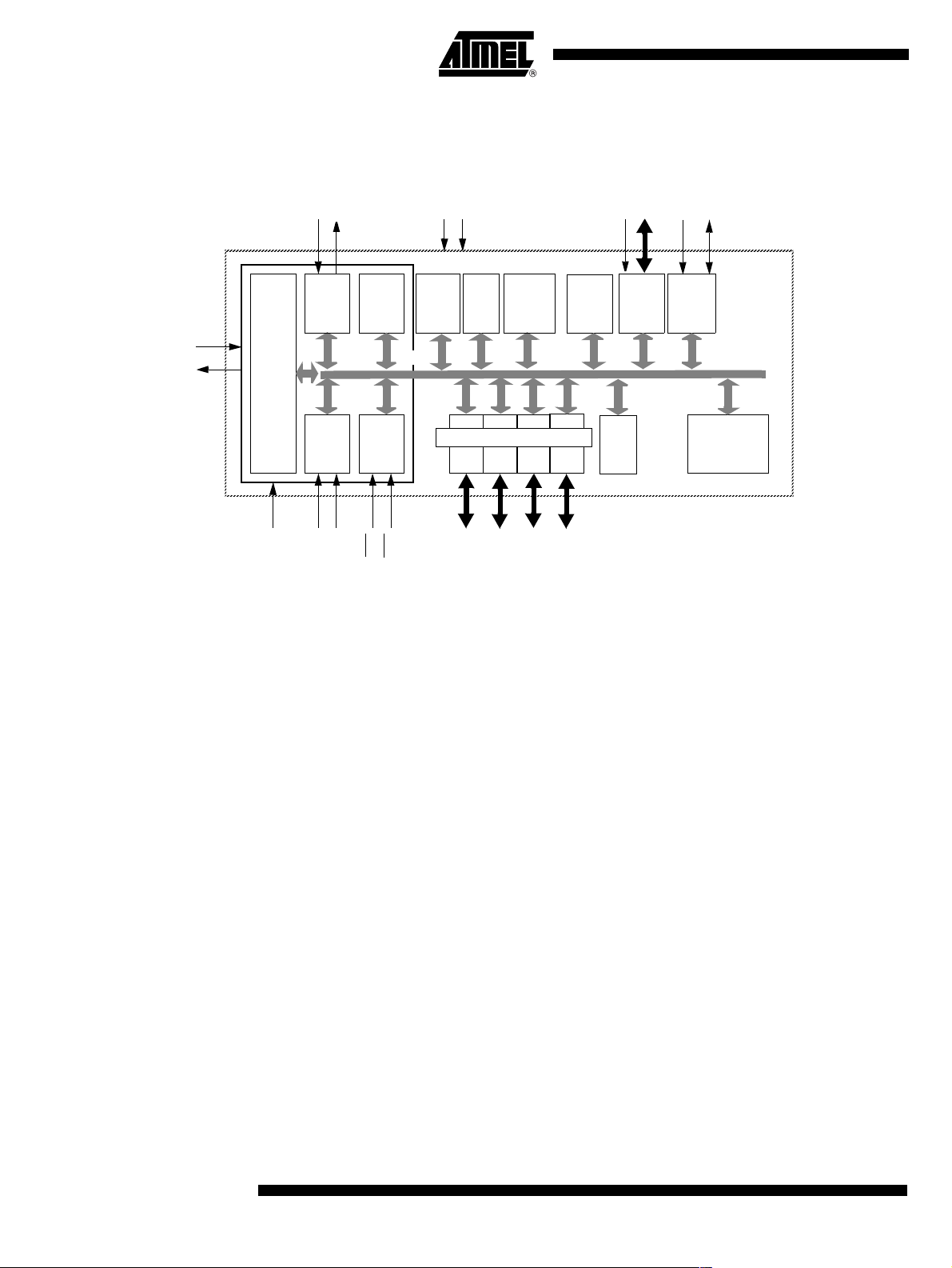
Block Diagram
In X2 mode a m aximum external clock rate of 20 MHz reaches a 300 ns cycle time.
PCA
Vss
RxD
TxD
Vcc
ECI
T2EX
T2
XTAL1
XTAL2
CPU
RESET
Notes: 1. 8 analog Inputs/8 Digital I/O
2. 2-Bit I/O Port
UART
Timer 0
Timer 1
T0
C51
CORE
T1
RAM
256x8
INT
Ctrl
INT0
INT1
Flash
Boot
16kx8
loader
2kx8
IB-bus
Parallel I/O Ports & Ext. Bus
Port 1
Port 2
(2)
(1)
P1
P2
EEPROM
2kx8
Port 3
P3
Port 4
ERAM
256x8
P4(2)
Watch
Dog
PCA
Timer2
10-bit
ADC
2
T89C5115
4128A–8051–04/02
Page 3
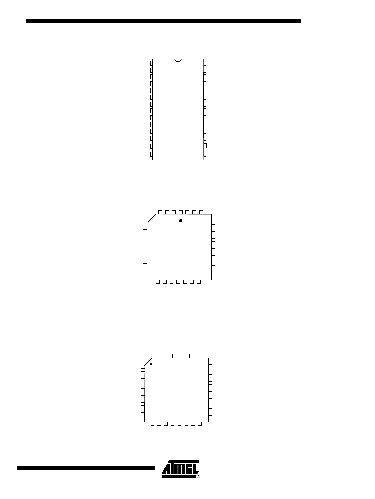
Pin Configuration
T89C5115
VAREF
VAGND
VAVCC
P3.5/T1
P3.4/T0
P3.3/INT1
P3.2/INT0
P3.1/TxD
P3.0/RxD
P4.0
P2.1
P3.7
P3.6
P3.5/T1
P3.4/T0
P3.3/INT1
P4.1
P4.0
P2.1
P3.7
P3.6
1
2
3
4
5
6
7
SO28
8
9
10
11
12
13
14
VAGND
VAVCC
P4.1
432
5
6
7
PLCC-28
8
9
10
11
12131415161718
P1.0 /AN0/T2
VAREF
1
282726
28
P1.0/
27
P1.1/AN1/T2EX
26
P1.2/AN2/ECI
25
P1.3/AN3/CEX0
P1.4/AN4/CE X1
24
P1.5/AN5
23
P1.6/AN6
22
P1.7/AN7
21
P2.0
20
RESE
19
18
VSS
VCC
17
XT AL1
16
XTAL2
15
P1.2 /AN2/ECI
P1.1 /AN1/T2E X
25
24
23
22
21
20
19
AN0/T2
T
P1.3/AN3/CEX0
P1.4/AN4/CEX1
P1.5/AN5
P1.6/AN6
P1.7/AN7
P2.0
RESET
4128A–8051–04/02
P4.0
P2.1
P3.7
P3.6
P3.5/T1
P3.4/T0
NC
P3.3/INT1
VSS
VCC
XTAL1
XTAL2
P3.1/TxD
P3.0/RxD
P3.2/INT0
P4.1
NC
VAREF
VAGND
VAVCC
30
31
32
1
2
3
4
5
6
7
8
9
101112
P3.1/TxD
P3.2/INT0
28
29
QFP-32
131415
NC
XTAL2
P3.0/RxD
P1.0/AN 0/T2
27
XTAL1
P1.2/AN2/ECI
P1.1/AN1/T2EX
25
26
P1.3/AN3/CEX0
24
P1.4/AN4/CEX1
23
P1.5/AN5/CEX2
22
P1.6/AN6/CEX3
21
P1.7/AN7/CEX4
20
P2.0
19
NC
18
RESET
17
16
VSS
VCC
3
Page 4

Table 1. Pin Description
Pin Name Type Description
VSS GND Circuit ground
VCC Supply Voltage
VAREF Reference Voltage for ADC
VAVCC Supply Voltage for ADC
VAGND Reference Ground for ADC
P1.0:7 I/O Port 1:
Is an 8-bit bi-directional I/O port with internalpull-ups. Port 1 pins can be used for
digital input/output or as analoginputs for the AnalogDigital Converter(ADC). Port 1
pins that have 1’s written to them are pulled high by the internal pull-up transistors
and can be used as inputs in this state. As inputs, Port 1 pins that are being pulled
lowexternallywillbethesourceof current(I
becauseof the internal pull-ups.Port 1 pins are assigned to be used as analog
inputs via the ADCCF register (in this case the internal pull-ups are disconnected).
As a secondary digitalfunction, port 1 containsthe Timer2 externalt rigger and clock
input; the PCA external clock input and the PCA module I/O.
P1.0/AN0/T2
Analoginput channel 0,
External clock input for Timer/counter2.
P1.1/AN1/T2EX
Analoginput channel 1,
Trigger input f or Timer/counter2.
P1.2/AN2/ECI
Analoginput channel 2,
PCA external clock input.
P1.3/AN3/CEX0
Analoginput channel 3,
PCA module 0 Entry of input/PWM output.
P1.4/AN4/CEX1
Analoginput channel 4,
PCA module 1 Entry of input/PWM output.
P1.5/AN5
Analoginput channel 5,
P1.6/AN6
Analoginput channel 6,
P1.7/AN7
Analoginput channel 7,
It can drive CMOS inputs without external pull-ups.
, see section"Electrical Characteristic")
IL
Port 2:
Is an 2-bit bi-directional I/O port with internalpull-ups. Port2 pins that have 1’s
writtento them are pulled high by the internalpull-ups andcan be used as inputsin
P2.0:7 I/O
4
T89C5115
this state. As inputs, Port 2 pins that are being pulled low externally will be a source
of current (IIL, on the datasheet) because of the internal pull-ups.
IntheT89C51CC02Port2cansinkorsource5mA.ItcandriveCMOSinputs
without external pull-ups.
4128A–8051–04/02
Page 5

Table 1. Pin Description (Continued)
Pin Name Type Description
P3.0:7 I/O Port 3:
Is an 8-bit bi-directional I/O port with internalpull-ups. Port3 pins that have 1’s
writtento them are pulledhigh by the internalpull-uptransistorsand can be used as
inputs in thisstate.As inputs, Port 3 pinsthatare beingpulledlowexternally will be a
sourceof current(I
pull-ups.
The outputlatchcorrespondingto a secondaryfunction must be programmedto one
for that function to operate (except for TxD ). The secondary functions are assigned
to the pins of port 3 as follows:
P3.0/RxD:
Receiver data input (asynchronous) or data input/output (synchronous) of the serial
interface
P3.1/TxD:
Transmitter data output (asynchronous) or clock output (synchronous) of the serial
interface
P3.2/INT0
External interrupt 0 input/timer 0 gate control input
P3.3/INT1
External interrupt 1 input/timer 1 gate control input
P3.4/T0:
Timer 0 counter input
P3.5/T1:
Timer 1 counter input
It can drive CMOS inputs without external pull-ups.
:
:
, see section "Electrical Characteristic") becauseof the internal
IL
T89C5115
P4.0:1 I/O
RESET I/O
XTAL1 I
XTAL2 O
Port 4:
Is an 2-bit bi-directional I/O port with internalpull-ups. Port4 pins that have 1’s
writtento them are pulled high by the internalpull-upsand can be used as inputsin
this state. As inputs, Port 4 pins that are being pulled low externally will be a source
of current (IIL, on the datasheet) because of the internal pull-up transistor.
It can drive CMOS inputs without external pull-ups.
Reset:
A high level on this pin during two machine cycles while the oscillator is running
resetsthe device. An internal pull-downresistorto VSS permitspower-onreset
using only an external capacitor to VCC.
XTAL1:
Input of the invertingoscillator amplifier and input of the internalclock generator
circuits. To drive the device from an external clock source, XTAL1 should be driven,
while XTAL2 is left unconnected. To operate above a frequency of 16 MHz, a duty
cycle of 50% should be maintained.
XTAL2:
Output from the inverting oscillator amplifier.
4128A–8051–04/02
5
Page 6

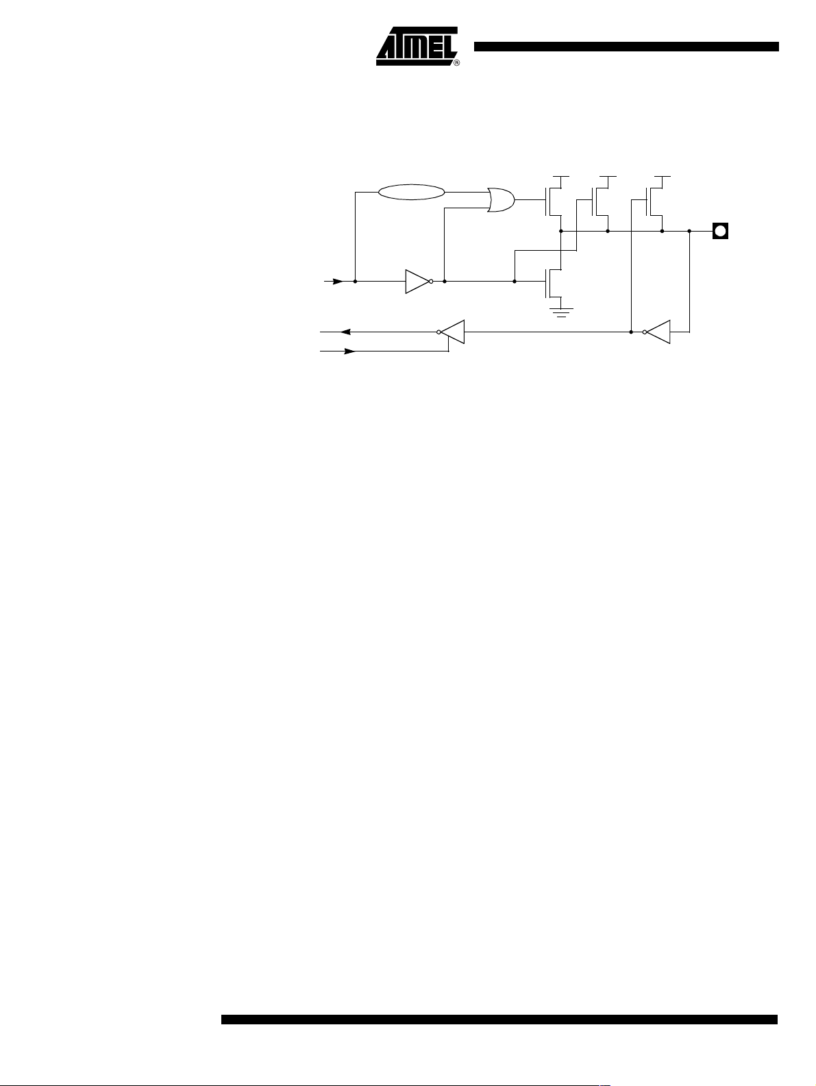
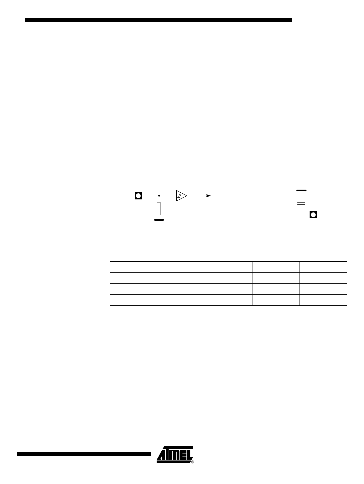
I/O Configurations Each Port SFR operates v ia type-D latches, as illustrated in Figure 1 f or Ports 3 and 4. A
CPU "write to latch" signal initiates transfer of internal bus data into t he type-D latch. A
CPU "read latch" signal transfers the latched Q output on to the internal b us. Sim ilarly, a
"read pin" signal transfers the logical level of the Port pin. Some Port data instructio ns
activate the "read latch" signal while others activate the "read pin" signal. Latch instructions are referre d to as R ead -Modif y-Writ e instructio ns. Each I/O line may be
independently programmed as input or output.
Port Structure Figure 1 shows the st ruc t ure of Ports, which have internal pull-ups. An external source
can pull the pin low. Each Port pin can be configured e ither for general-purpose I/O or
for its alternate input output function.
To use a pin for general-purpose output, set or clear the corresponding bit in the Px register (x = 1 to 4). T o use a pin for general-purpose input, se t the bit in the Px register.
This turns off the output FET drive.
To configure a pin for its alternate function, set the bit in the Px register. When the latch
is set, the "alternate output f unc tion" signal controls the outp ut level (see Figure 1). The
operation of Ports is discussed further in "quasi-Bidirectional Port Operation" p aragraph.
Figure 1. Ports Structure
VCC
READ
LATCH
INTERNAL
BUS
WRITE
TO
LATCH
READ
PIN
D
CL
LATCH
ALTERNATE
OUTPUT
FUNCTION
Q
ALTERNATE
INPUT
FUNCTION
INTERNAL
PULL-UP (1)
Note: The internal pull-up can be disabled on P1 when analog function is selected.
P1.x
P2.x
P3.x
P4.x
6
T89C5115
4128A–8051–04/02
Page 7

T89C5115
Read-Modify-Write Instructions
Some instruction s read the latch da ta rather than the pin data. The latch based instructions read the data, modify the data and then rewrite the latch. These are called "ReadModify-Write" instructions. B elow is a complete list of these special instructions (see
Table ). When the destination operand is a Port or a Port bit, t hes e instructions read the
latch rather than the pin:
Table 2. Read-Modify-Write Instructions
Instruction Description Example
ANL logical A ND ANL P1, A
ORL logical OR ORL P2, A
XRL logical E X-OR XRL P3, A
JBC jump if bit = 1 and clear bit JBC P1.1, LABEL
CPL complement bit CPL P3.0
INC increment INC P2
DEC decrement DEC P2
DJNZ decrement and jump if not zero DJNZ P3, LABEL
MOV Px.y, C move carry bit to bit y of Port x MOV P1.5, C
CLR Px.y clear bit y of Port x CLR P2.4
SET Px.y set bit y of Port x SET P3.3
Quasi-bidirectional Port Operation
It is not obvious the last three instructions in this l ist are Read-Modify-Write instructions.
These instructions read the port (all 8 bits), modify the specifically addressed bit and
write the new byte back to the la tch. These Read-Modify-Write inst ruc tions are directed
to the latch rather than the pin in order to av oid possible misinterpretation of voltage
(and therefore, logic) levels at the pin. For example, a Port bit used to drive the base of
an external bipolar transistor can not rise above the transistor’s base-emitter junction
voltage (a value lower than VIL). With a lo gic one written to the bit, attempts by the CPU
to read the Port at the pin are misinterpreted as logic zero. A read of the latch rather
than the pins r eturns the correct logic-one v alue.
Port 1, Port 3 and Port 4 have fixed internal pull-ups and are referred to as "quasi-bidirectional" Ports. When c onfigured as an input, the pin impedance appears as logic one
and sources current in response to an external logic zero condition. Resets write logic
one to all Port latches. If logical zero is subsequently written to a Port latch, it can be
returned to input conditions by a logical one written to the latch.
Note: Port latch values change near the end of Read-Modify-Write insruction cycles. Output
buffers (and therefore t he pin state) update early in the instruction after Read-ModifyWrite instruction cycle.
Logical zero-to-one transitions in Port 1, Port 3 and Port 4 use an additional pull-up (p1)
to aid this logic transition see Figure 2. This increases s witch speed. This extra pull-up
sources 100 times normal internal ci rc uit cu rrent du ring 2 oscillator clo c k periods. The
internal pull-ups are fi eld-effect tr ans istors rather than linear resistors. Pull-ups consist
of t hree p-channel FET (pFET) devices. A pFET is on when the gate senses logical zero
and off when the gat e senses logical one. pFET #1 is turned on for two oscillator periods
immediately after a z ero-to-one transition in the Port l atch. A logic al one at the Port pin
turns on pFET #3 (a weak pull-up) through the inverter. This inverter and pFET pair form
a latch to drive logical one. pFET #2 is a very weak pull-up switched on whene ver the
4128A–8051–04/02
7
Page 8
associated nFET is switched off. This is traditional CMOS switch convention. Current
strengths are 1/10 that of pFET #3
Figure 2. Internal Pull-Up Configurations
2 Osc. PERIODS
VCCVCCVCC
OUTPUT DATA
INPUTDATA
READ PIN
p1(1)
n
p2
p3
P1.x
P2.x
P3.x
P4.x
8
T89C5115
4128A–8051–04/02
Page 9

T89C5115
SFR Mapping The Special Function Registers (SFRs) o f the T8 9C5115 fall into t he following
categories:
Table 3. C51CoreSFRs
MnemonicAddName 76543210
ACCE0hAccumulator ––––––––
B F0hBRegister ––––––––
PSW D0h Program Status Word CY AC F0 RS1 RS0 OV F1 P
SP81hStackPointer ––––––––
Data Po inter Low
DPL 82h
DPH 83h
byte
LSB of DPTR
Data Pointer High
byte
MSB of DPTR
––––––––
––––––––
Table 4. I/O Port SFRs
MnemonicAddName 76543210
P190hPort1 ––––––––
P2A0hPort2(x2) ––––––––
P3B0hPort3 ––––––––
P4C0hPort4(x2) ––––––––
Table 5. Timers SFRs
MnemonicAddName 76543210
TH0 8Ch
TL0 8Ah
TH1 8Dh
TL1 8Bh
TH2 CDh
Timer/Counter0High
byte
Timer/Counter 0 Low
byte
Timer/Counter1High
byte
Timer/Counter 1 Low
byte
Timer/Counter2High
byte
––––––––
––––––––
––––––––
––––––––
––––––––
TL2 CCh
TCON 88h
TMOD 89h
4128A–8051–04/02
Timer/Counter 2 Low
byte
Timer/Counter 0 and
1 control
Timer/Counter 0 and
1 Modes
––––––––
TF1 TR1 TF0 TR0 IE1 IT1 IE0 IT0
GATE1 C/T1# M11 M01 GATE0 C/T0# M10 M00
9
Page 10

Table 5. Timers SFRs (Continued)
MnemonicAddName 76543210
T2CON C8h
T2MOD C9h
RCAP2H CBh
RCAP2L CAh
WDTRST A6h
WDTPRG A7h
Timer/Counter 2
control
Timer/Counter 2
Mode
Timer/Counter 2
Reload/Capture High
byte
Timer/Counter 2
Reload/Capture Low
byte
WatchDog Timer
Reset
WatchDog Timer
Program
TF2 EXF2 RCLK TCLK EXEN2 TR2 C/T2# CP/RL2#
––––––T2OEDCEN
––––––––
––––––––
––––––––
–––––S2S1S0
Table 6. Serial I/O Port SFRs
MnemonicAddName 76543210
SCON 98h Serial Control FE/SM0 SM1 SM2 REN TB8 RB8 TI RI
SBUF99hSerialDataBuffer––––––––
SADENB9hSlaveAddressMask––––––––
SADDRA9hSlaveAddress ––––––––
Table 7. PCA SFRs
Mnemo
-nicAddName 76543210
CCON D8h PCA Timer/Counter Control CF CR – CCF4 CCF3 CCF2 CCF1 CCF0
CMOD D9h PCA Timer/Counter Mode CIDL WDTE – – – CPS1 CPS0 ECF
CLE9hPCATimer/CounterLowbyte ––––––––
CH F9h PCA Timer/Counter High byte – – – – – – – –
CCAPM0
CCAPM1
CCAP0H
CCAP1H
CCAP0L
CCAP1L
DAh
PCA Timer/Counter Mode 0
DBh
PCA Timer/Counter Mode 1
FAh
PCA Compare Capture Module 0 H
FBh
PCA Compare Capture Module 1 H
EAh
PCA Compare Capture Module 0 L
EBh
PCA Compare Capture Module 1 L
–
CCAP0H7
CCAP1H7
CCAP0L7
CCAP1L7
ECOM0
ECOM1
CCAP0H6
CCAP1H6
CCAP0L6
CCAP1L6
CAPP0
CAPP1
CCAP0H5
CCAP1H5
CCAP0L5
CCAP1L5
CAPN0
CAPN1
CCAP0H4
CCAP1H4
CCAP0L4
CCAP1L4
MAT0
MAT1
CCAP0H3
CCAP1H3
CCAP0L3
CCAP1L3
TOG0
TOG1
CCAP0H2
CCAP1H2
CCAP0L2
CCAP1L2
PWM0
PWM1
CCAP0H1
CCAP1H1
CCAP0L1
CCAP1L1
ECCF0
ECCF1
CCAP0H0
CCAP1H0
CCAP0L0
CCAP1L0
10
T89C5115
4128A–8051–04/02
Page 11

T89C5115
Table 8. Interrupt SFRs
MnemonicAddName 76543210
IEN0 A8h
IEN1 E8h
IPL0 B8h
IPH0 B7h
IPL1 F8h
IPH1 F7h
Interrupt Enable
Control 0
Interrupt Enable
Control 1
Interrupt Priority
Control Low 0
Interrupt Priority
Control High 0
Interrupt Priority
Control Low 1
Interrupt Priority
Control High1
EA EC ET2 ES ET1 EX1 ET0 EX0
––––––EADC–
– PPC PT2 PS PT1 PX1 PT0 PX0
– PPCH PT2H PSH PT1H PX1H PT0H PX0H
––––––PADCL–
––––––PADCH–
Table 9. ADC SFRs
MnemonicAddName 76543210
ADCON F3h ADC Control – PSIDLE ADEN ADEOC ADSST SCH2 SCH1 SCH0
ADCF F6h ADC Configuration CH7 CH6 CH5 CH4 CH3 CH2 CH1 CH0
ADCLK F2h ADC Clock – – – PRS4 PRS3 PRS2 PRS1 PRS0
ADDH F5h ADC Data High byte ADAT9 ADAT8 ADAT7 ADAT6 ADAT5 ADAT4 ADAT3 ADAT2
ADDLF4hADCDataLowbyte––––––ADAT1ADAT0
Table 10. Other SFRs
MnemonicAddName 76543210
PCON 87h PowerControl SMOD1 SMOD0 – POF GF1 GF0 PD IDL
AUXR1 A2h Auxiliary Register 1 – – ENBOOT – GF3 0 – DPS
CKCON 8Fh Clock Control – WDX2 PCAX2 SIX2 T2X2 T1X 2 T0X2 X2
FCON D1h Flash Control FPL3 FPL2 FPL1 FPL0 FPS FMOD1 FMOD0 FBUSY
EECON D2h EEPROM Contol EEPL3 EEPL2 EEPL1 EEPL0 – – EEE EEBUSY
4128A–8051–04/02
11
Page 12

Table 11. SFR Mapping
(1)
0/8
1/9 2/A 3/B 4/C 5/D 6/E 7/F
F8h
F0h
E8h
E0h
D8h
D0h
C8h
C0h
B8h
B0h
A8h
IPL1
xxxx x000
B
0000 0000
IEN1
xxxx x000
ACC
0000 0000
CCON
0000 0000
PSW
0000 0000
T2CON
0000 0000
P4
xxxx xx11
IPL0
x000 0000
P3
1111 1111
IEN0
0000 0000
CH
0000 0000
CL
0000 0000
CMOD
00xx x000
FCON
0000 0000
T2MOD
xxxx xx00
SADEN
0000 0000
SADDR
0000 0000
CCAP0H
0000 0000
ADCLK
xxx0 0000
CCAP0L
0000 0000
CCAPM0
x000 0000
EECON
xxxx xx00
RCAP2L
0000 0000
CCAP1H
0000 0000
ADCON
x000 0000
CCAP1L
0000 0000
CCAPM1
x000 0000
RCAP2H
0000 0000
ADDL
0000 0000
TL2
0000 0000
ADDH
0000 0000
TH2
0000 0000
ADCF
0000 0000
IPH1
xxxx x000
IPH0
x000 0000
FFh
F7h
EFh
E7h
DF
h
D7h
CF
h
C7h
BFh
B7h
AFh
A0h
98h
90h
88h
80h
P2
1111 1111
SCON
0000 0000
P1
1111 1111
TCON
0000 0000
P0
1111 1111
(1)
0/8
SBUF
0000 0000
TMOD
0000 0000
SP
0000 0111
1/9 2/A 3/B 4/C 5/D 6/E 7/F
AUXR1
xxxx 00x0
TL0
0000 0000
DPL
0000 0000
Reserved
Note: 1. These registers are bit-addressable.
Sixteen addresses in the SFR space are both byte-addressable and bit-addressable. The bit-addressable SFR’s are those
whose address ends in 0 and 8. The bit addresses, in this area, are 0x80 through to 0xFF.
TL1
0000 0000
DPH
0000 0000
TH0
0000 0000
TH1
0000 0000
WDTRST
1111 1111
WDTPRG
xxxx x000
CKCON
0000 0000
PCON
00x1 0000
A7h
9Fh
97h
8Fh
87h
12
T89C5115
4128A–8051–04/02
Page 13

T89C5115
Clock The T89C5115 core needs only 6 clock periods per machine cycle. This feature, called
‘X2’, provides the following advantages:
• Divides frequency crystals by 2 (cheaper crystals) while keeping the same CPU
power.
• Saves power consumption while keepi ng the same CPU power (os cillator power
saving).
• Saves power consumption by dividing dynam ic operat ing frequenc y by 2 in
operating and idle modes.
• Increases CPU power by 2 while keeping the same crystal frequency.
In order to keep the original C51 compatibility, a divider-by-2 is inserted between the
XTAL1 signal and the main cloc k input of the core (phase generator). This divider may
be disabled by the software.
An extra feature is available to start after Reset in the X2 mode. This feature can be
enabled by a bit X2B in the Hardware Security Byte. This bit is desc ribed in the section
"In-System Programming".
Description The X2 bit in the CKCON register (see Table 12) allows switching from 12 clock cycles
per i ns truct ion to 6 clock cycles and vice vers a. At reset, the stan dard speed is activated
(STD mode).
Setting this bit activates the X2 feature (X2 mode) for the C PU Clock only (see Figure
3.).
The Timers 0, 1 and 2, Uart, PCA or WatchDog switch in X2 mode only if the corresponding bit is cleared in the CKCON register.
The clock for the whole circuit and peripheral is f irst divided by two bef ore being used by
the CPU core and peripherals. This allows any cyclic ratio to be accepted on the XTAL1
input. In X2 mode, as this divider is bypassed, the signals on XTAL1 must have a cyclic
ratio b et ween 40 to 60%. Fi gure 3. shows the cloc k generation block diagram. The X2
bit is validated on the XTAL1÷2 rising edge to avoid glitches when switching from the X2
to the S TD m ode. Figure 4 shows the mode switching waveforms.
4128A–8051–04/02
13
Page 14
Figure 3. Clock CPU Generation Diagram
XTAL1
XTAL2
PD
PCON.1
÷ 2
X2B
Hardware byte
X2
CKCON.0
÷ 2
1
0
On RESET
÷ 2
÷ 2
1
0
0
1
÷ 2
1
0
PCON.0
IDL
÷ 2
1
0
÷ 2
1
0
CPU Core
Clock
CLOCK
CPU Core Clock Symbol
and ADC
1
0
FT0 Clock
FT1 Clock
FT2 Clock
FUart Clock
FPca Clock
FWd Clock
CPU
14
X2
CKCON.0
T89C5115
WDX2
CKCON.6
PCAX2
CKCON.5
SIX2
CKCON.4
T2X2
CKCON.3
T1X2
CKCON.2
PERIPH
CLOCK
Peripheral Clock Symbol
T0X2
CKCON.1
4128A–8051–04/02
Page 15
T89C5115
Figure 4. Mode Switching Waveforms
XTAL1
XTAL2
X2 bit
CPU
clock
STD
Mode
Note: In order to prevent any incorrect operation while operating in the X2 mode, users must be aware that all peripherals using the
clock frequency as a time reference (UART, timers...) will have their time reference divided by two. For example a free running
timer generating an interrupt every 20 ms will then generate an i nterrupt every 10 ms. A UART with a 4800 baud rate will have
a 9600 baud rate.
X2
Mode
STD
Mode
4128A–8051–04/02
15
Page 16

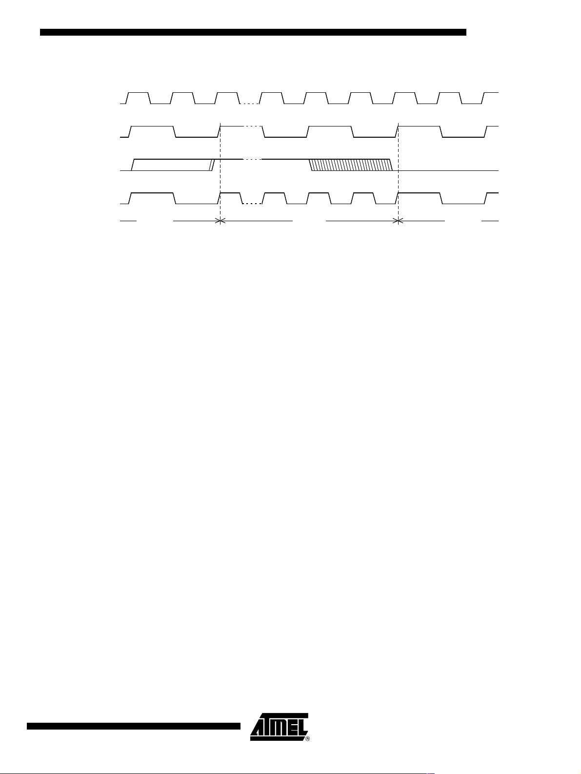
Register Table 12. CKCON Register
CKCON (S:8Fh)
Clock Control Register
76543210
– WDX2 PCAX2 SIX2 T2X2 T1X2 T0X2 X2
Bit
Number
7-
6WDX2
5 PCAX2
4SIX2
3T2X2
2T1X2
1T0X2
0X2
Bit
Mnemonic Description
Reserved
The value readfrom this bit is indeterminate. Do not set this bit.
WatchDog clock
Clear to select6 clock periods per peripheral clock cycle.
Set to select 12 clock periods per peripheral clock cycle.
Programmable Counter Array clock
Clear to select6 clock periods per peripheral clock cycle.
Set to select 12 clock periods per peripheral clock cycle.
Enhanced UART clock (MODE 0 an d 2 )
Clear to select6 clock periods per peripheral clock cycle.
Set to select 12 clock periods per peripheral clock cycle.
Timer2 clock
Clear to select6 clock periods per peripheral clock cycle.
Set to select 12 clock periods per peripheral clock cycle.
Timer1 clock
Clear to select6 clock periods per peripheral clock cycle.
Set to select 12 clock periods per peripheral clock cycle.
Timer0 clock
Clear to select6 clock periods per peripheral clock cycle.
Set to select 12 clock periods per peripheral clock cycle.
CPU clock
Clear to select 12 clock periods per machine cycle (STD mode) for CPU and all
the peripherals.
Set to select 6 clock periods per machine cycle(X2 mode) and to enable the
individual peripherals "X2"bits.
(1)
(1)
(1)
(1)
(1)
(1)
16
Notes: 1. This control bit is validated when the CPU clock bit X2 is set; when X2 is l ow, this bit
has no effect.
Reset Value = x000 0000b
T89C5115
4128A–8051–04/02
Page 17
T89C5115
Power Management
Introduction Two po w er reduction modes are implemented in the T89C5115: the Idle mode an d the
Power-down mode. T hese modes are detailed in the following sections. In addition to
these power reduction modes, t he clocks of the core and peripherals can be dynamically
divided by 2 using the X2 mode detailed in Section “Clock”.
Reset A reset i s required after app lying power at turn-on. T o achieve a valid reset, the reset
signal mus t be maintained for a t least 2 m achine cycles (24 o scillat or clock periods)
while the oscillator is running and stabilized and VCC established within the specified
operating ranges. A device reset initializes the T89C5115 and vectors the CPU to
address 0000h. RST input has a pull-down resistor allowing power-on reset by simply
connecting an external capacitor to V
characteristics are discussed in the Section “DC Characteristics” of the T89C5115
datasheet. The status of the Port pins during res et is detailed in Table 13.
Figure 5. Reset Circuitry and Power-On Reset
as shown in Figure 5. Resistor value and input
DD
Reset Recommendation to Prevent Flash Corruption
VDD
+
RST
b. Power-on Reseta. RST i nput circuitry
RST
VSS
To CPU core
and peripherals
RST
R
Table 13. Pi n Co nditions in Sp ec ial Operating Modes
Mode Port 1 Port 2 Port 3 Port 4
Reset High High High High
Idle Data Data Data Data
Power-downDataDataDataData
A bad reset sequence will lead to bad micr oco ntrol ler initialization and system registers
like SFR’s, Pr ogram Counter, etc. will not be correctly initialized. A bad initialization may
lead to unpredictable behaviour of the C51 microcontroller.
An example of this s ituat ion m ay occur in an instance where the bit ENBOOT in AUXR1
register is initialized fr om the hardware bit BLJB upon reset. Since this bit allow s mapping of the bootloader in the code area, a r es et fail ure can be critical.
4128A–8051–04/02
If one wants the ENBOOT cleared inorder to unmap the boot from the code area (yet
due to a bad reset) the bit ENBOOT in SFR’s may be set. If the value of Program
Counter is accidently in the range of the boot memory addresses then a flash access
(write or erase) m ay corrupt the Flash on-chip memory .
It is recommended to use an external reset circuitry featuring power sup ply monitoring to
prevent system malfunction during periods of insufficient power supply voltage(power
supply failure, power supply switched off).
17
Page 18

Idle Mode Idle mode is a power reduction mode that reduces the power consumption. In this mode,
program execution halts. Idle mode freezes the clock to the CPU at known states while
the peripherals continue to be clocked. The CPU status before entering Idle mode is
preserved, i.e., the program counter and program status word regis t er retain their data
for the duration of Idle mode. The contents of the
status of the Port pins during I dle mo de is detailed in Table 13.
Entering Idle Mode To enter Idle mode, s et the IDL bit in PCON register (see Table 14). The T89C5115
enters Idle mode upon execution of the instruction that sets IDL bit. The in struction that
sets IDL bit is the l as t instruction executed.
Note: If IDL bit and PD bit are set simultaneously, the T89C5115 enters Power-down mode.
Then it does not go in Idle mode when exitingPower-down mode.
Exiting Idle Mode There are two ways to exit Idle mode:
1. Generate an enabled interrupt.
– Hardware clears IDL bit in PCON register which restores the clock to the
CPU. Execution resumes with the interrupt service routine. Upo n completion
of t he interrupt service routine, program execution resum es with the
instruction immediately following the instruction that activated Idle mode.
The gene ral-purpose flags (GF1 and GF0 in PCON register) may be used to
indicate whether an interrupt occurred during normal operation or during Idle
mode. When Idle mode is exited by an interrupt, the interrupt service routine
may examine GF1 and GF0.
2. Generate a reset.
– A logic high on the RST pin clears IDL bit in P CON r egister directly and
asynchronously. This restores the clock to the CPU. Program execution
momentarily resumes with the instruction im mediately following the
instruction that ac tivated the Idle m ode and may continue for a number of
clock cycles before the internal reset algorithm takes control. Reset
initializes the T89C5115 and vectors t he CPU t o addres s C:0000h.
SFRs and RA M are also retained. The
Note: During the time that execution resumes, the internal RAM cannot be accessed; however,
it is possible for the Port pins to be accessed. To avoid unexpected outputs at the Port
pins, the instruction immediately following the instruction that activatedIdle m ode should
notwritetoaPortpinortotheexternalRAM.
Power-down Mode The Power-down mode places the T89C5115 in a very low power state. Power-down
mode stops the os cillator, freezes all clock at known states. The CPU status pr ior t o
entering Power-down mode is preserv ed, i.e., the program counter, program status
word register retain their data for the duration of Power-down mode. In addition, the
SFRs and RAM contents are preserved. The status of the Port pins during Power-down
mode is detailed in Table 13.
Note: VDDmaybereducedtoaslowasV
power dissipation. Take care, however, that VDD is not reduced until Power-down mode
is invoked.
Entering Power-down Mo de To enter Power-down mode, set PD bit in PCON register. The T89C5115 enters the
Power-down mode upon execution of the instruction that sets PD bit. The instruction
that sets PD bit is the last instruction executed.
18
T89C5115
during Power-down mode to further reduce
RET
4128A–8051–04/02
Page 19
T89C5115
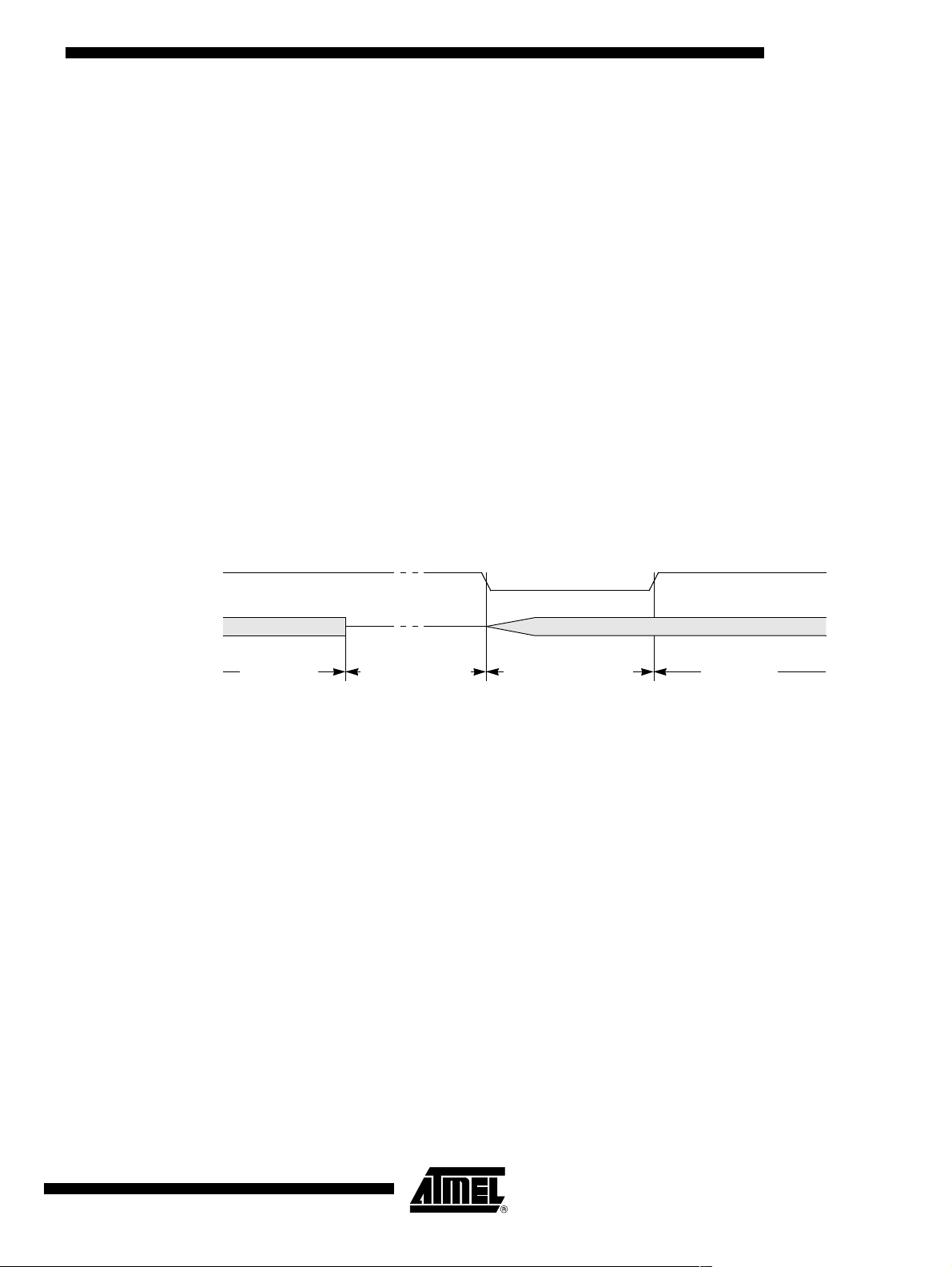
Exiting Power-down Mode Note: If VDD was reduced during the Power-down mode, do not exit Power-down mode until
VDD is r estored to the normal operating level.
There are t w o way s to exit the Power-down mode:
1. Generate an enabled external interrupt.
– The T89C5115 provides capability to exit from Power-down using INT0#,
INT1#.
Hardware clears PD bit in PCON register which starts the os c il lator and
restores the clocks to the CPU and peripherals. Usin g
resumes when the input is released (s ee Fi gure 6). Execution resumes with
the interrupt service routine. Upon completion of the interrupt service
routine, program execution resumes with the instruction immedia tely
following the instruction that activated Power-do w n mode.
Notes: 1. The external interrupt used to exit Power-down mode m ust be configured as level
sensitive (INT0# and INT1#) and m ust be assigned the highest priority. In addition,
the duration of the interrupt must be long enough to allow the oscillator to stabilize.
The execution will only resume when the interrupt is deasserted.
2. Exit from power-down by external interrupt does not affect t he
RAM content.
INTx# input, execution
SFRs nor the internal
Figure 6. Power-down Exit Waveform Using INT1:0#
INT1:0#
OSC
Power-down phase Oscillatorrestartphase Active phaseActive phase
2. Generate a reset.
– A logic hi gh on the RST pin clears PD bit in PCON register directly and
asynchronously. This starts the oscillator and restores the clock to the CPU
and peripherals. Program execution momentarily resumes with the
instruction im mediately following the instruction that ac t ivate d Powe r-do wn
mode and may continue for a number of clock cycles before the internal
reset algorithm takes control. Reset initializes the T89C5115and vectors the
CPU to address 0000h.
Notes: 1. During t he time that execution resumes, the internal RAM cannot be accessed; how-
ever, it is possible for the Port pins to be accessed. To avoid unexpected outputs at
the Port pins, the instruction immediately following the instruction that activated the
Power-down mode should not write to a Port pin or t o the external RAM.
2. Exit from power-down by reset redefines all the
RAM content.
SFRs, but does not affect t he internal
4128A–8051–04/02
19
Page 20

Registers PCON (S:87h)
Table 14. PCON Register
Power Configuration Register
76543210
––––GF1GF0PDIDL
Bit
Number
7-4
3GF1
2GF0
1PD
0IDL
Bit
Mnemonic Description
Reserved
–
The value readfrom these bits is indeterminate.Do not set these bits.
General-purpose flag 1
One use is t o indicate whetheran interrupt occurred duringnormal operation or
during Idle mode.
General-purpose flag 0
One use is t o indicate whetheran interrupt occurred duringnormal operation or
during Idle mode.
Power-down Mode bit
Cleared by hardware when an interrupt or reset occurs.
Set to activate the Power-down mode.
If IDL and PD are both set, PD takes precedence.
Idle Mode bit
Cleared by hardware when an interrupt or reset occurs.
Set to activate the Idle mode.
If IDL and PD are both set, PD takes precedence.
Reset Value = XXXX 0000b
20
T89C5115
4128A–8051–04/02
Page 21

Data Memory The T89C5115 provides data memory access in two different spaces:
The internal space mapped in three separate segments:
• the lower 128 bytes RAM segment.
• the upper 128 bytes RAM segmen t.
• the expanded 256 bytes RAM segment (ERAM) .
A f ourth internal seg ment is availabl e but dedicated to Speci al Function Regi sters,
SFRs, (addresses 80h to FFh) ac c es sible by direct addressing mode.
Figure 7 shows the internal data memory spaces organization.
Figure 7. Internal Memory – RAM
T89C5115
FFh
00h
256 bytes
Internal ERAM
FFh
80h 80h
7Fh
00h
Upper
128 bytes
Internal RAM
indirect addressing
Lower
128 bytes
Internal RAM
director indirect
addressing
FFh
directaddressing
Special
Function
Registers
Internal Space
Lower 128 Bytes RAM The lower 128 bytes of RAM (see Figure 7) are accessible from address 00h to 7Fh
using direct or indirect addressing modes . The lowest 32 bytes are grouped into 4 banks
of 8 registers (R0 to R7). Two bits RS0 and RS1 in PSW register (see Figure 16) select
which bank is in use according to T able . This allows more ef fic ient use of code space,
since register instructions are shorter t han inst r uc tions that use direct addressing, and
can be used for c ont ex t switching in interrupt service routines.
Table 15. Register B ank Selection
RS1 RS0 De scription
0 0 Register bank 0 from 00h to 07h
0 1 Register bank 0 from 08h to 0Fh
4128A–8051–04/02
1 0 Register bank 0 from 10h to 17h
1 1 Register bank 0 from 18h to 1Fh
The next 16 bytes above the register banks form a block of bit-addressable memory
space. The C51 instruction set includes a wide s election of single-bit instructions , and
the 128 bits in this area can be directly addressed by these instructions. The bit
addresses in this area are 00h to 7Fh.
21
Page 22

Figure 8. Lower 128 bytes Internal RAM Organization
7Fh
30h
20h
18h
10h
08h
00h
2Fh
Bit-Addressable Space
(Bit Addresses 0-7Fh)
1Fh
17h
4Banksof
8Registers
0Fh
R0-R7
07h
Upper 128 Bytes RAM The upper 128 bytes of RAM are accessible from address 80h to FFh using only indirect
addressing mode.
Expanded RAM The on-chip 256 bytes of expanded RAM (E R AM) are accessible from address 0000h to
00FFh using indirect addressing mode thro ugh MOVX instructions. In this addres s
range.
Note: Lower 128 bytes RAM, Upper 128 bytes RAM, and expanded RAM are made of volatile
memory cells. This m eans that the RAM content is indeterminate after power-up and
must then be i nitialized properly.
22
T89C5115
4128A–8051–04/02
Page 23
T89C5115
Dual Data Pointer
Description The T89 C5115 implements a second data pointer for s peeding up code execution and
reducing code size in case of intensive usage of external memory accesses.
DPTR0 and DPTR1 are seen by the CPU as DPTR and are accessed using the SFR
addresses 83h and 84h that are t he DPH and DPL addresses. The DPS bit i n AUXR1
register (see Figure 17) is used to select whether DPTR is the data pointer 0 or the data
pointer 1 (see Figure 9).
Figure 9. Dual Data Pointer Implementation
DPL0
DPL1
DPTR0
DPTR1
DPH0
DPH1
0
1
DPS
0
1
DPL
AUXR1.0
DPH
DPTR
Application Software can take advant age of the additional data pointers to both increase speed and
reduce code size, for example, block operations (cop y , compare…) are well served by
using one data pointer as a “source” pointer and the other one as a “destination” pointer.
Hereafter is an example of block mov e implementation using t he two pointers and coded
in assem bler. The latest C compiler tak es also adv antage of this feature by providin g
enhanced algorithm libraries.
The INC instruction is a short (2 bytes) an d fast (6 machine cycle) way to manipulate t he
DPS bit in the AUXR1 register. However, note that the INC instruction does not directly
force the DPS bit to a particular state, but simply toggles it. In simple routines, such as
the block move example, only the fact that DPS is toggled in the proper sequence matters, not its actual value. In other words, the block move rout ine works the same whether
DPS is '0' or '1' on entry.
4128A–8051–04/02
; ASCII block move using dual data pointers
; Modifies DPTR0, DPTR1, A and PSW
; Ends when encountering NULL character
; Note: DPS exits opposite to the entry state unless an extra INC AUXR1 is
added
AUXR1EQU0A2h
move:movDPTR,#SOURCE ; address of SOURCE
incAUXR1 ; switch data pointers
movDPTR,#DEST ; address of DEST
mv_loop:incAUXR1; switch data pointers
movxA,@DPTR; get a byte from SOURCE
incDPTR; increment SOURCE address
incAUXR1; switch data pointers
movx@DPTR,A; write the byte to DEST
incDPTR; increment DEST address
jnzmv_loop; check for NULL terminator
end_move:
23
Page 24

Registers Table 16. PSW Register
PSW (S:8Eh)
Program Status Word Register
76543210
CY AC F0 RS1 RS0 OV F1 P
Bit
Number
7CY
6AC
5F0User De finable Flag 0
4-3 RS1:0
2OV
1F1User De finable Flag 1
0P
Bit
Mnemonic Description
Carry Flag
Carry out from bit 1 of ALU operands.
Auxiliary Carry Flag
Carry out from bit 1 of addition operands.
Register Bank Select Bits
Refer to Table for bits description.
Overflow Flag
Overflow set by arithmetic operations.
Parity Bit
Set when ACC contains an odd numberof 1’s.
Cleared when ACC contains an even number of 1’s.
Reset Value = 0000 0000b
24
T89C5115
4128A–8051–04/02
Page 25

T89C5115
Table 17. AUX R 1 R egister
AUXR1 (S:A2h)
Auxiliary Control Register 1
76543210
– – ENBOOT – GF3 0 – DPS
Bit
Number
7-6
5 ENBOOT
4
3GF3General-purpose Flag 3.
20
1 – Reserved for Data Pointer Extension.
0DPS
Bit
Mnemonic Description
Reserved
–
The value readfrom these bits is indeterminate.Do not set these bits.
Enable Boot Flash
Set this bit for map the boot flash between F800h -FFFFh
Clearthis bit for disable boot flash.
Reserved
–
The value readfrom this bit is indeterminate. Do not set this bit.
Always Zero
This bit is stuck to logic 0 to allow INC AUXR1 instruction without affecting GF3
flag.
Data Pointer Select Bit
Set to select second dual data pointer: DPTR1.
Clear to selectfirst dual data pointer:DPTR0.
Reset Value = xxxx 00x0b
4128A–8051–04/02
25
Page 26

EEPROM Data Memory
The 2-kbyte on-c hip EEPROM memory block is located at addres se s 0000h to 07FFh of
the XRAM /ERAM memory space and is selected by setting control bits i n the EECON
register. A read in the EE PRO M m emory is done with a MOVX ins truction.
A physical write in the EEPROM memory i s done in two steps: write data in the column
latches and transfer of all data latches into an EEPROM memory row (programming).
The number of data written on the page may vary from 1 up to 128 bytes (the page
size). When programming, only the data writt en in the column latch is programmed and
a ninth bit is used to obtain t his feature. This provides the capability to program the
whole memory by bytes, by pa ge or by a number of bytes in a page. Indeed, each ninth
bit is set when the writing the corresponding byte in a row and all these ninth bits are
reset after t he w riting of the complete EEPROM row.
Write Data in the Column Latches
Data i s written by byte to the column latches as for an external RAM memory. Out of the
11 address bits of the data pointer, the 4 MSBs are used for page selection (row) and 7
are used for byte selection. Between two EEPROM programming sessions, all the
addresses in the column latches must stay on the same page , meaning th at the 4 MSB
must no be changed.
The following procedure is used to write to the column latches:
• Save and disable interrupt.
• Set bit EEE of EECON register
• Load DPTR with the address to write
• Store A register with the data to be written
• Execute a MOVX @DPTR, A
• If needed loop the three last instructions until the end of a 128 byt es page
• Restore interrupt.
Note: The last page address used when loading the column latch is the one used to select the
page programming address.
Programming The EEPROM programming co ns ists of the following actions:
• writing one or more bytes of one page in the column latc hes . Norm ally, all bytes
must belong to the same page; if not, th e first page address will be latched and the
others disc arded.
• launching programming by writing the control seque nc e (50h followed by A0h) to the
EECON register.
• EEBUSY flag in EECON is then set by hardware to indicate that programming is in
progress and that t he EEPROM segment is not available for reading.
• The end of programming is indicated by a hardware clear of the E EBUSY flag.
Note: The sequence 5xh and Axh must be executed without instructions between them, other-
wise the programming is aborted.
Read Data The following procedure is used to read t he data stored in the EEPROM m emory:
• Save and disable interrupt
• Set bit EEE of EECON register
• Load DPTR with the address to read
• Execute a MOVX A, @DPTR
• Restore interrupt
26
T89C5115
4128A–8051–04/02
Page 27

T89C5115
Examples ;*F*************************************************************************
;* NAME: api_rd_eeprom_byte
;* DPTR contain address to read.
;* Acc contain the reading value
;* NOTE: before execute this function, be sure the EEPROM is not BUSY
;***************************************************************************
api_rd_eeprom_byte:
MOV EECON, #02h; map EEPROM in XRAM space
MOVX A, @DPTR
MOV EECON, #00h; unmap EEPROM
ret
;*F*************************************************************************
;* NAME: api_ld_eeprom_cl
;* DPTR contain address to load
;* Acc contain value to load
;* NOTE: in this example we load only 1 byte, but it is possible upto
;* 128 bytes.
;* before execute this function, be sure the EEPROM is not BUSY
;***************************************************************************
api_ld_eeprom_cl:
MOV EECON, #02h ; map EEPROM in XRAM space
MOVX @DPTR, A
MOVEECON, #00h; unmap EEPROM
ret
;*F*************************************************************************
;* NAME: api_wr_eeprom
;* NOTE: before execute this function, be sure the EEPROM is not BUSY
;***************************************************************************
api_wr_eeprom:
MOV EECON, #050h
MOV EECON, #0A0h
ret
4128A–8051–04/02
27
Page 28

Registers Table 18. EECON Register
EECON (S:0D2h)
EEPROM Control Register
76543210
EEPL3 EEPL2 EEPL1 EEPL0 - - EEE EEBUSY
Bit
Bit Number
Mnemonic Description
7-4 EEPL3-0
3-
2-
1 EEE
0 EEBUSY
Programming Launch Command bits
Write 5Xh followed by AXh to EEPL to launch the programming.
Reserved
The value read from this bit is indeterminate. Do not set this bit.
Reserved
The value read from this bit is indeterminate. Do not set this bit.
Enable EEPROM Space bit
SettomaptheEEPROMspaceduringMOVXinstructions(Writeinthecolumn
latches).
Clear to map the XRAM space during MOVX.
Programming Busy flag
Set by hardware when programming is in progress.
Cleared by hardware when programming is done.
Can not be set or cleared by software.
Reset Value = XXXX XX00b
Not bit addressable
28
T89C5115
4128A–8051–04/02
Page 29
T89C5115
Program/Code Memory
Flash Memory Architecture
The T89C5115 implement 16-KB of on-chip program/code memory .
The Flash memory increases EPROM and ROM functionality by in-circuit electrical era-
sure and programming. Thanks to t he internal charge pump, the high voltage needed for
programming or erasing Flash cells is generated on-chi p using the s tandard VDD voltage. Thus, the Flash Memory can be programmed using only one voltage and allows InSystem Programming c ommonly known as ISP. Hardware programming mode is also
available using specific programming tool.
Figure 10. Program/Code Memory Organization
3FFFh
16-KB
internal
Flash
0000h
T89C5115 features two on-chip flash memories:
• Flash memory FM0:
containing 1 6-KB of program me mory (use r space) organized into pages 128 bytes
• Flash memory FM1:
2K B y tes for boot loader and Application Programming Interfaces (API).
The FM0 can b e program by bot h parallel programming and S erial In-System Program ming (ISP) whereas FM1 supports only parallel programmi ng by p rogramm ers . The ISP
mode is detailed in the "In-System Programming" section.
All Read/Write access operations on Fl as h Memo ry by user application are managed by
a set of AP I described in t he "In-Sy s tem Programming" section.
Figure 11. Flash Memory Architecture
Hardware Security (1 byte)
Extra Row (128 bytes)
Column Latches (128 bytes)
3FFFh
0000h
16-KB
Flash memory
user space
FM0
2K Bytes
Flash memory
boot space
FM1
FM1 mapped between FFFFh and
F800h when bit ENBOOT is set in
AUXR1 register
FFFFh
F800h
4128A–8051–04/02
29
Page 30

FM0 Memory Architecture The Flash memory is made up of 4 blocks (see Figure 11):
1. The memory array (user space) 16-KB.
2. The Extra Row.
3. The Hardware security bits.
4. The column latch registers.
User S pac e This space is composed of a 16-KB Flash memory organized in 128 pages of 128 bytes.
It contains the user’s application c ode.
Extra Row (XROW) This row is a part of FM0 and has a size of 128 bytes. The extra row may contain infor-
mation for boot loader usage.
Hardware security Byte The Hardware Security Byte space is a part of FM0 an d has a size of 1 byte.
The 4 MSB can be read/written by softw are, the 4 LSB can only be read by software and
written by hardware in parallel m ode.
Column Latches The column latches, also part of FM0, have a size of f ull page (128 bytes).
The column latches are the entrance buffers of the three previous memory locations
(user array, XROW and Hardware security byte).
Cross Flash Memory Access
Description
The FM0 memory can be program only from FM1. Programm ing FM0 from FM0 or from
external memory is impossible.
The FM1 memory can be program only by parallel programming.
The Table 19 show all software flash access allowed.
Table 19. Cross Flash Memory Access
Codeexecutingfrom
FM0
(user Flash)
FM1
(boot flash)
Action
Read ok -
Load column latch ok -
Write - Read ok ok
Load column latch ok -
Write ok -
FM0
(user Flash)
FM1
(boot Flash)
30
T89C5115
4128A–8051–04/02
Page 31

T89C5115
Overview of FM0 Operations
The CPU interfaces to the Flash memory through the FCON register and AUXR1
register.
These registers are used to:
• Map the memory spaces in the adressable space
• Launch the programming of the memo ry spaces
• Get the status of the flash memory (busy/not busy)
Mapping of the Memory Space By default, the user space is accessed by MO VC instruction for read only. The colum n
latches space is m ade accessible by setting the FPS bit in FCON register. W riting is
possible from 0000h to 3FFFh, address bits 6 to 0 are used to s elect an address w ithin a
page while bits 14 t o 7 are used to select the programming address of the page.
Setting FPS bit takes precedence on the EEE bit in EECON register.
The oth er memory spaces (user, extra row, hardware security) are made acces s ible in
the code segment by programming bits FMOD0 and F MOD1 in FCON register in accordance with Table 20. A MOVC instruction is then used for reading these spaces.
Table 20. FM0 B locks Select Bits
FMOD1 FMOD0 FM0 Adressable space
0 0 User (0000h-3FFFh)
0 1 Extra Row(FF80h-FFFFh)
1 0 Hardware Security Byte (0000h)
11reserved
Launching Programming FPL3:0 bits in F CON register are used to secure the launch of programming. A specific
sequence must be written in these bits to unlock the write protection and to launch the
programming. This s equence is 5xh followed by Axh. Table 21 summarizes the memory
spaces to program according to FMOD1:0 bits.
Table 21. Programming Spaces
Write to FCON
OperationFPL3:0 FPS FMOD1 FMOD0
5 X 0 0 No action
User
Extra Row
Hardware
Security
Byte
Reserved
AX00
5 X 0 1 No action
AX01
5 X 1 0 No action
A X 1 0 Write the fuse bits space
5 X 1 1 No action
A X 1 1 No action
Write the column latches in user
space
Write the column latches in extra row
space
4128A–8051–04/02
Note: The sequence 5xh and Axh must be executing without instructions between them other-
wise the programming is aborted.
31
Page 32

Interrupts that may occur during programming time must be disabled to avoid any spurious exit of the programming mode.
Status of the Flash Memory T he bit FBUSY in FCON register is used to indicate the status of programming.
FBUSY is set when programming is in progres s .
Selecting FM1 The bit ENBOOT in AUXR1 register is used to map FM1 from F800h to FFFFh.
Loading the Column Latches Any number of data from 1 byte to 128 bytes can be loaded in the c olumn latches. This
provides the capability to program the whole memory by byte, by page or by any num ber
of bytes in a page.
When programming is launched, an automatic erase of the locations loaded in the column latches is fi rs t performed, then programming is effectively d one. Thus no page or
block erase is needed and only the loa ded data are programmed in the corresponding
page.
The following proced ur e is us ed to load th e column latches and is sum ma ri zed in
Figure 12:
• Disable interrupt and map the column latch space by setting FPS bit.
• Load the DPTR with the address to load.
• Load Accumulator register with the data to load.
• Execute the MOVX @DPTR, A instruction.
• If needed loop the three last instructions until the page is completely loaded.
• unmap the column latch and Enable Interrupt
32
T89C5115
4128A–8051–04/02
Page 33

Figure 12. Column Latches Loading Procedu re
Column Latches
Loading
Save & Disable IT
EA= 0
Column Latches Mapping
FCON = 08h (FPS=1)
Data Load
DPTR= Address
ACC= Data
Exec:MOVX@DPTR,A
Last Byte
to load?
T89C5115
Data memory Mapping
FCON = 00h (FPS = 0)
Restore IT
Note: The last page address used when loading the column latch is the one used to select the
page programming address.
Programming the Flash Spaces
User The following procedure is used to program the User space a nd is sum mar ize d in
Figure 13:
• Load up to one page of data in the column latches from address 0000h to 3FFFh.
• Disable the interrupts.
• Launch the programming by writing the data sequence 50h followed by A0h in
FCON register (only f rom F M1).
The end of the program ming indicated by the FBUSY flag cleared.
• Enable the interrupts.
Extra Row The following procedure is used to program the Extra Row space and is summ arized i n
Figure 13:
• Load data in the column latches from address FF80h to FFFFh.
• Disable the interrupts.
• Launch the programming by writing the data sequence 52h followed by A2h in
FCON register (only f rom F M1).
The end of the program ming indicated by the FBUSY flag cleared.
• Enable the interrupts.
4128A–8051–04/02
33
Page 34

Figure 13. Flash and Extra row Programming Procedure
Flash Spaces
Programming
Column Latches Loading
see Figure 12
Save & Disable IT
EA= 0
Launch Programming
FCON= 5xh
FCON= Axh
FBusy
Cleared?
Clear Mode
FCON = 00h
Hardware Security Byte
End Programming
Restore IT
The following procedure is used to program the Hardware Secur ity Byte space
and is summarized in Figure 14:
• Set FPS and map Hardware byte (FCON = 0x0C)
• Save and disable the interrupts.
• Load DPTR at address 0000h.
• Load Accumulator register with the data to load.
• Execute the MOVX @DPTR, A instruction.
• Launch the programming by writing the data sequence 54h followed by A4h in
FCON register (only f rom F M1).
The end of the programming indicated by the FBusy flag cleared.
• Restore the interrupts
34
T89C5115
4128A–8051–04/02
Page 35

Figure 14. Hardware Programming Procedure
Flash Spaces
Programming
Save & Disable IT
EA= 0
FCON = 0Ch
T89C5115
Save & Disable IT
EA= 0
Launch Programming
FCON= 54h
FCON= A4h
Data Load
DPTR= 00h
ACC= Data
Exec:MOVX@DPTR,A
End Loading
Restore IT
FBusy
Cleared?
Clear Mode
FCON = 00h
End Programming
RestoreIT
Reading the Flash Spaces
User The following procedure is used to r ead t he U se r space:
• Read one byte in Accumulator by executing MOVC A,@A+DPTR with
A+DPTR=read@.
Note: FCON is s upposed to be reset when not needed.
Extra Row The following procedure is used to read the Extra Row space and is summarized in
Figure 15:
• Map the Extra Row space by writing 02h in FCO N reg ister.
• Read one byte in Accumulator by executing MOVC A,@A+DPTR with A= 0 &
DPTR= F F80h to FFFFh.
• Clear FCON to unmap the Extra Row.
Hardware Security Byte
4128A–8051–04/02
The following proc ed ur e is used to re ad the Hardwar e Security space and is
summarized in Figure 15:
• Map the Hardware Security space by writing 04h in FCON register.
• Read the byte i n Accumulator by executing MOVC A,@A+DPTR with A= 0 &
DPTR= 0000h.
• Clear FCON to unmap the Hardware Security Byte.
35
Page 36

Figure 15. Reading Procedure
FlashSpaces Reading
Flash Spaces Mapping
FCON= 00000xx0b
Data Read
DPTR= Address
ACC= 0
Exec:MOVCA,@A+DPTR
Clear Mode
FCON = 00h
Flash Protection from P arallel
Programming
The t hree lock bits in Hardware Security Byte (see "In-System Programming" section)
are programmed according to Tabl e 22 provide different level of protection for the o nchip code and data located in FM0 and FM1.
The only way to write this bits are the parallel mode. They are set by default to level 3.
Table 22. Program Lock bit
Program Lock Bits
Security
level
1UUU
2 P U U Parallelprogramming of the Flash is disabled.
3UPU
LB0 LB1 LB2
Protection Description
No program lock features enabled. MOVC instruction executed from
external program memory returns non encrypted data.
Same as 2, also verify through parallel programminginterface is
disabled.
Program Lock bits
U: unprogrammed
P: programmed
WARNING: Security level 2 and 3 should only be programmed after F lash and Core
verification.
Preventing Flash Corruption See paragraph in the "Power Management" section, page 17.
36
T89C5115
4128A–8051–04/02
Page 37

Registers FCON Register
FCON (S:D1h)
Flash Control Register
76543210
FPL3 FPL2 FPL1 FPL0 FPS FMOD1 FMOD0 FBUSY
T89C5115
Bit
Number
7-4 FPL3:0
3FPS
2-1 FMOD1:0
0 FBUSY
Bit
Mnemonic Description
Programming Launch Command Bits
Write 5Xh followed by AXh to launch the programming according to FMOD1:0.
(see Table 21.)
FlashMap Program Space
Set to map the column latch space in the data memory space.
Clear to re-map the data memory space.
Flash Mode
See Table 20 or Table 21.
Flash Busy
Set by hardware when programming is in progress.
Clearby hardwarewhen programming is done.
Can not be changedby software.
Reset Value = 0000 0000b
4128A–8051–04/02
37
Page 38

In-System Programming (ISP)
With the implementation of the User Space (FM0) and the Boot Space (FM1) in Flash
technology the T89C5115 allows the system engineer the development of applications
with a very high level of flexibility. This flexibility is based on the possibility to alter the
customer program at any stages of a product’s life:
• Before assembly the 1st personalization of the product by programming in the FM0
and if needed also a customized Boot loader in the FM1.
Atmel provide also a standard Boot loader by default UART
• After assembling on the PCB in its final embedded position by serial mode via the
UART.
This In-System Programming (ISP) allows code modification over the total lifetime of the
product.
Besides the default Boot loader Atmel provide to the customer also all the needed Application-Programming-Interfaces (API) which are needed for the ISP. The API are located
also in the Boot memory.
This allow the c us tomer to have a f ull use of the 16-Kbyte user memory.
Flash Programming and Erasure
There are three methods of programming the Flash memory:
• The Atmel bootloader located in FM1 is activated by the application. Low level API
routines (located in FM1)wil l be used to program FM0. The interface used for serial
downloading to FM0 is the UA RT. API can be called also by user’s bootloader
locatedin FM0 at [SBV]00h.
• A further method exist in activating the Atmel boot loader by hardware activation.
• The FM0 can be programmed also by the parallel mode using a programmer.
Figure 16. Flash Memory Mapping
FFFFh
2K Bytes IAP
bootloader
F800h
3FFFh
Custom
Boot Loader
[SBV]00h
16-KB
FM1
FM1 mapped between F800h and FFFFh
when API called
38
Flash memory
FM0
0000h
T89C5115
4128A–8051–04/02
Page 39

Boot Process
T89C5115
Software Boot P rocess
Example
Many algorithms can be used for the software boot process. Before describing them,
The description of the different flags and bytes is given below:
Boot Loader Jump Bit (BLJB):
- This bit indicates if on RESET the user wants to jump to this application at address
@0000h on FM0 or execute the boot loader at address @F800h on FM1.
- BLJB = 0 on p arts delivered with bootloade r programm ed.
- To read or m odify this bit, the APIs are used.
Boot Vector Address (SBV):
- This byte c ontains the MSB of the user boot loader address in FM0.
- The default value of SBV is FFh (no user boot loader in FM0).
- To read or m odify this byte, the APIs are used.
Extra Byte (EB) & Boot Status Byte (BSB):
- These bytes are res erv ed for customer use.
- To read or m odify these bytes, the APIs are used.
Figure 17. Hardware Boot Process Algorithm
RESET
bit ENB OOT in AUXR1 register
is initialized with BLJB.
Hardware
ENBOOT = 0
PC = 0000h
BLJB == 0
?
ENBOOT = 1
PC = F800h
Application
Software
in FM0
Boot Loader
in FM1
4128A–8051–04/02
39
Page 40

Application Programming Interface
Several Application Program Interface (API) calls are av ailable for use by an application
program to permit selective erasing and programming of Flash pages . All calls are made
by functions.
All APIs are descr ibe in: "In-System Programing: Flash Library for T89C5115", available
on the Atmel web site at www.atmel.com.
Table 23. List of API
API Call Description
PROGRAM DATABYTE Write a byte in flash memory
PROGRAM DATA PAGE Write a page (128 bytes) in flash memory
PROGRAM EEPROM BYTE Write a byte in Eeprom memory
ERASE BLOCK Erase all flash memory
ERASE BOOT VECTOR (SBV) Erase the boot vector
PROGRAM BOOT VECTOR (SBV) Write the boot vector
PROGRAM EXTRA BYTE (EB) Write the extra byte
READ DATA BYTE –
READ EEPROM BYTE –
READ FAMILY CODE –
READ MANUFACTURER CODE –
READ PRODUCT NAME –
READ REVISION NUMBER –
READ STATUS BIT (BSB) Read the status bit
READ BOOT VECTOR (SBV) Read the boot vector
READ EXTRA BYTE (EB) Read the extra byte
PROGRAM X2 Write the hardware flag for X2 mode
READ X2 Read the hardware flag for X2 mode
START BOOTLOADER T o start the bootloader from the application
XROW Bytes Table 24. XROW Mapping
Mnemonic Description Defaultvalue Address
– Copy of the Manufacturer Code 58h 30h
– Copy of the Device ID#1: Family code D7h 31h
– Copy of the Device ID#2: Memoriessize and type BBh 60h
– Copy of the Device ID#3: Name and Revision FFh 61h
40
T89C5115
4128A–8051–04/02
Page 41

Hardware Security Byte Table 25. Hardware Security byte
76543210
X2B BLJB - - - LB2 LB1 LB0
T89C5115
Bit
Number
7X2B
6BLJB
5-3 -
2-0 LB2:0 Lock Bits
Bit
Mnemonic Description
X2 Bit
Set this bit to start in standard mode
Clearthis bit to start in X2 mode.
Boot Loader Jump Bit
- 1: To start the user’s application on next RESET (@0000h) located in FM0,
- 0: Tostartthe boot loader(@F800h) located in FM1.
Reserved
The value readfrom these bits are indeterminate.
Default value after erasing chip: FFh
Notes: 1. Onlythe 4 MSB bits can be accessed by software.
2. The 4 LSB bits can only be accessed by parallel mode.
4128A–8051–04/02
41
Page 42

Serial I/O Port The T89C5115 I/O serial port is compatible with the I/O serial port in the 80C52.
It provid es both synchronous and asynchronous communication modes. It operates as a
Universal Asynchronous Receiver and Transmitter (UART) in three full-duplex modes
(Modes 1, 2 and 3). Asynchronous transmission and recept ion can oc c ur simultaneously
and at different baud rates
Serial I/O port includes the following enhancements:
• Framing error detection
• Automatic address recognition
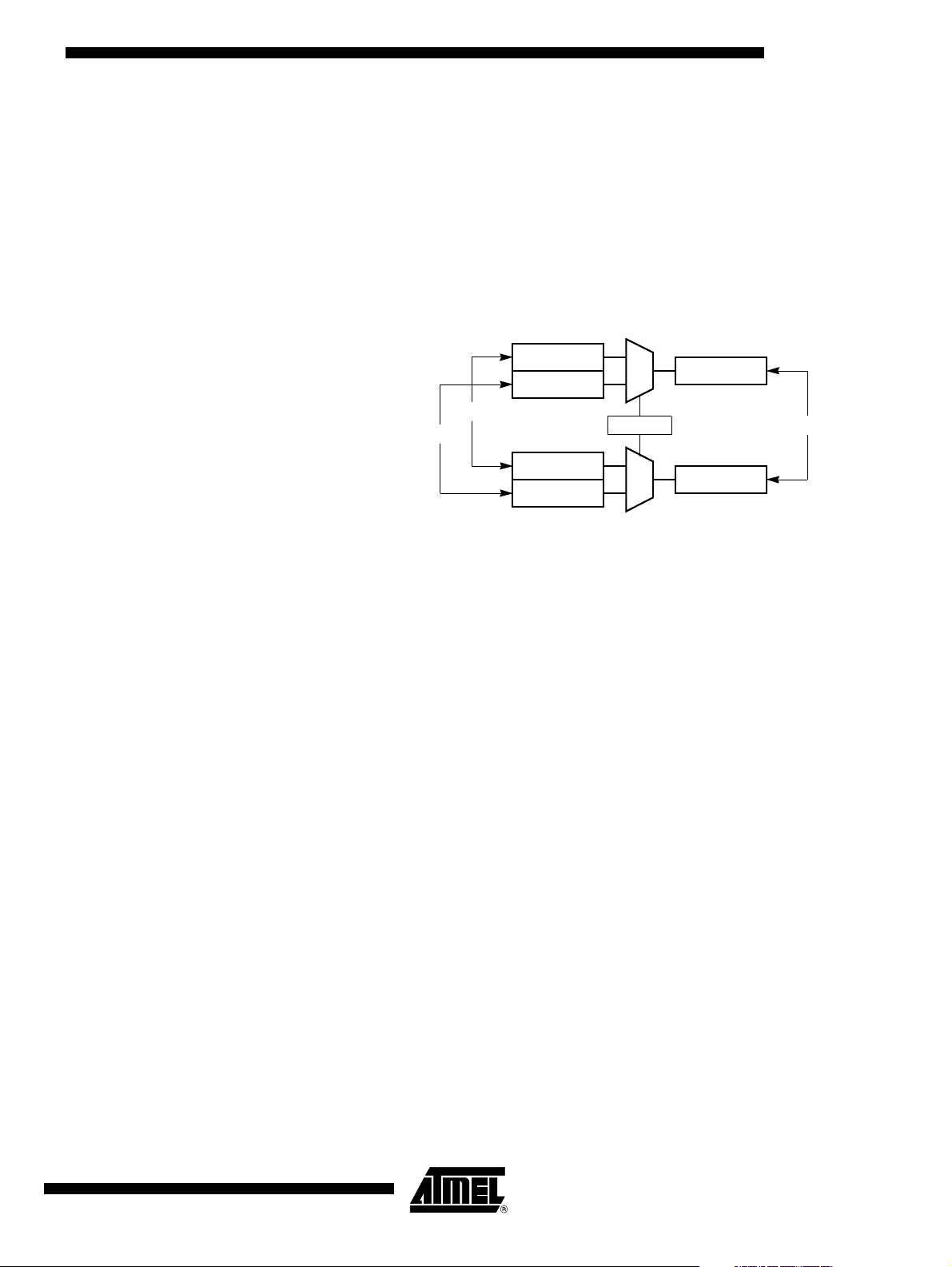
Figure 18. Serial I/O Port Block Diagram
IB Bus
TXD
RXD
SBUF
Transmitter
Write SBUF
Mode 0 Transmit
RI
TI
SBUF
Receiver
Receive
Shift register
Read SBUF
Load SBUF
Serial Port
Interrupt Request
Framing Error Detection Framing bit error detection is provided for the three asynchronous modes. To enable t he
framing bit error detection feature, s et SM OD0 bit in PCON register.
Figure 19. Framing Error Block Diagram
RITIRB8TB8RENSM2SM1SM0/FE
Set FE bit if stop bit is 0 (framing error)
42
SM0toUARTmodecontrol
IDLPDGF0GF1POF-SMOD0SMOD1
To UARTframingerror control
When this feature is enabled, the receiver checks each incoming data frame for a valid
stop bit. An invalid stop bit may result from noise on the serial lines or from simultaneous
transmission by t wo CPUs. If a valid stop bit is not found, the Framing Error bit (FE) in
SCON register bit is set.
The software may examine the F E bit af ter each reception to check for data errors.
Once set, only software or a reset clears the F E bit. Subsequently received f rames with
T89C5115
4128A–8051–04/02
Page 43

T89C5115
valid stop bits cannot clear the FE bit. Wh en the FE feature is enabled, RI rises on the
stop bit instead of t he last data bit (See Figure 20 and Figure 21).
Figure 20. UART Timing in Mode 1
Automatic Address Recognition
RXD
RI
SMOD0=X
FE
SMOD0=1
Start
bit
Data byte
D7D6D5D4D3D2D1D0
Stop
bit
Figure 21. UART Timing in Modes 2 and 3
RXD
RI
SMOD0=0
RI
SMOD0=1
FE
SMOD0=1
Start
bit
Data byte Ninth
D8D7D6D5D4D3D2D1D0
Stop
bit
bit
The automatic address recognition feature is enabled when the mul tipro ce ssor communication feature is enabled (SM2 bit in SCO N register is set).
Implemented in t he hardw are, automatic address recognition enhances the multiprocessor c ommunication feature by allowing the serial port to examine the address of each
incoming command frame. Only when the serial port rec ognizes its own address will t he
receiver set the RI bit in the SCON register to generate an interrupt. This ensures that
the CPU is not interrupted by command frames addressed to other devices.
4128A–8051–04/02
If necessary, you can enable the automatic address recognition feature in mode 1. In
this configurati on, the stop bit takes the place of the ninth dat a bit. Bit RI is set only when
the received command frame address matches the device’s address and is terminated
by a valid stop bit.
To support automatic address recognition, a device is identified b y a given address and
a broadcast address.
Note: The multiprocessor communication and automatic address recognition features cannot
be enabled in mode 0 (i.e. setting SM2 bit in SCON register in mode 0 has no effect).
43
Page 44

Given Address Each d evice has a n individual address that is specified in the SADD R register; the
SADEN register is a mask byte that contains don’t-care bits (defined by zeros) to form
the device’s given address . The don’t-care bits provide the flexibility to address one or
more slaves at a t im e. T he following example illustrates how a given addres s is formed.
To address a device by its individual address, the SADEN mask by te must be 1111
1111b.
For example:
SADDR0101 0110b
SADEN
1111 1100b
Given0101 01XXb
Here is an example of how to use given addresses to address different slaves:
Slave A:SADDR1111 0001b
SADEN
1111 1010b
Given1111 0X0Xb
Slave B:SADDR1111 0011b
SADEN
1111 1001b
Given1111 0XX1b
Slave C:SADDR1111 0010b
SADEN
1111 1101b
Given1111 00X1b
The SADEN byte is selected so that each slave may be addressed separately.
For slave A, bit 0 (the LSB) is a don’t-care bit; for slaves B and C, bit 0 is a 1. To c om-
municate with slave A only, the mastermust send an address where bit 0 is clear (e.g.
1111 0000b).
For slav e A, bit 1 is a 0; for slaves B and C, bit 1 is a don’t care bit. To communicate with
slaves A and B, but not slave C, the master m us t send an address with bits 0 and 1 both
set (e.g. 1111 0011b).
To communicate with slaves A, B and C, the master must send an address with bit 0 s et,
bit 1 clear, and bit 2 clear (e.g. 1111 0001b).
Broadcast Address A broadcast address is formed from the logical OR of the SADDR an d SADE N registers
with zeros defined as don’t-care bits, e.g.:
SADDR 0101 0110b
SADEN 1111 1100b
SADDR OR SADEN1111 111Xb
The use of don’t-care bits provides flexibility in defining the broadcast address, however
in most applications, a broadcast address is FFh. The following is an example of using
broadcast addresses:
Slave A:SADDR1111 0001b
SADEN
1111 1010b
Given1111 1X11b,
Slave B:SADDR1111 0011b
SADEN
1111 1001b
Given1111 1X11B,
44
T89C5115
Slave C:SADDR=1111 0010b
SADEN
1111 1101b
Given1111 1111b
4128A–8051–04/02
Page 45

For slaves A and B, bit 2 is a don’t care bit; for slave C, bit 2 is set. T o communicate with
all of the slaves, the master must send an address FFh. To c ommunicate with slaves A
and B, but not slave C, the master can send and address FBh.
Registers Table 26. SCON Register
SCON (S:98h)
Serial Control Register
76543210
FE/SM0 SM1 SM2 REN TB8 RB8 TI RI
T89C5115
Bit
Number
7FE
–SM0
6SM1
5SM2
4REN
3TB8
2RB8
Bit
Mnemonic Description
Framing Error bit (SMOD0 = 1)
Cleartoresettheerrorstate,notclearedbyavalidstopbit.
Set by hardware when an invalid stop bit is detected.
Serial port Mode bit 0 (SMOD0 = 0)
Refer to SM1 for serial port mode selection.
Serial port Mode bit 1
SM0
SM1 Mode Baud Rate
0 0 ShiftRegister F
0 1 8-bit UART Variable
1 0 9-bit UART F
1 1 9-bit UART Variable
Serial port Mode 2 bit/Multiprocessor Communication Enable bit
Clearto disablemultiprocessorcommunication feature.
Set to enable multiprocessor communication feature in mode 2 and 3.
Reception Enablebit
Clearto disable serial reception.
Set to enable serial reception.
Transmitter Bit 8/Ninth bit to transmit in modes 2 and 3
Clearto transmit a logic0 in the 9th bit.
Set to transmit a logic 1 in the 9th bit.
Receiver Bit 8/Ninth bit received in modes 2 and 3
Cleared by hardware if 9th bit received is a logic 0.
Set by hardware if 9th bit receivedis a logic 1.
XTAL
XTAL
/12 (or F
/64 or F
/6 in mode X2)
XTAL
/32
XTAL
4128A–8051–04/02
Transmit Interrupt flag
1TI
0RI
Clear to acknowledge interrupt.
Set by hardware at the end of the 8th bit time in mode 0 or at the beginning of the
stop bit in the other modes.
Receive Interrupt flag
Clear to acknowledge interrupt.
Set by hardware at the end of the 8th bit time in mode 0, see Figure 20 and
Figure21 in the other modes.
Reset Value = 0000 0000b
Bit addressable
45
Page 46

Table 27. SADE N Register
SADEN (S:B9h)
Slave Address Mask Register
76543210
Bit
Number
7-0 – Mask Data for Slave Individual Address
Bit
Mnemonic Description
Reset Value = 0000 0000b
Not bit addressable
Table 28. SADDR Register
SADDR (S:A9h)
Slave Address Register
76543210
Bit
Number
7-0 – Slave I ndividualAddress
Bit
Mnemonic Description
Reset Value = 0000 0000b
Not bit addressable
Table 29. SBUF Reg ister
46
T89C5115
SBUF (S:99h)
Serial Data Buffer
76543210
––––––––
Bit
Number
7-0 – Data sent/received by Serial I/O Port
Bit
Mnemonic Description
Reset Value = 0000 0000b
Not bit addressable
4128A–8051–04/02
Page 47

T89C5115
Table 30. PCON Register
PCON (S:87h)
Power Control Register
76543210
SMOD1 SMOD0 - POF GF1 GF0 PD IDL
Bit
Number
7SMOD1
6SMOD0
5-
4POF
3GF1
2GF0
1PD
0IDL
Bit
Mnemonic Description
Serial port Mode bit 1
Settoselectdoublebaudrateinmode1,2or3.
Serial port Mode bit 0
Clear to selectSM0 bit in SCON register.
Set to select FE bit in SCON register.
Reserved
The value readfrom this bit is indeterminate. Do not set this bit.
Power-Off Flag
Clear to recognize next reset type.
Set by hardwarewhen VCC rises from 0 to its nominal voltage.Can also be set
by software.
General-purpose Flag
Cleared by user for general-purpose usage.
Set by user for general-purpose usage.
General-purpose Flag
Cleared by user for general-purpose usage.
Set by user for general-purpose usage.
Power-downmode bit
Cleared by hardwarewhen reset occurs.
Set to enter power-down mode.
Idle mode bit
Clear by hardwarewhen interruptor reset occurs.
Set to enter idle mode.
4128A–8051–04/02
Reset Value = 00x1 0000b
Not bit addressable
47
Page 48

Timers/Counters T he T89C5115 implements two g eneral-purpose, 16-bit Timers/Counters. Such are
identified a s Timer 0 and Timer 1, and can be independently configured t o operate in a
variety of mode s as a Timer or an eve nt Counter. When opera ting as a Timer, the
Timer/Counter runs for a programmed length of time, then issues an i nt errupt req uest.
When operating as a Counter, the Timer/Count er counts negative transit ions on an
external pin. After a pres et number of counts, the Counter issues an interrupt request.
The v arious operating mod es of each T imer/Coun ter are described in the fol lowing
sections.
Timer/Counter Operations
A bas ic operation is Timer r egist ers THx and TLx (x= 0, 1) co nnected in cascade to form
a 16-b it Timer. Setting the run control bit (TRx) in TCON register (see Figure 31) turns
the Timer on by allowing the selected input to increment TLx. When TLx overflows it
increments THx; when THx overflows it sets the Timer overflow flag (TFx) in TCON register. S etting the TRx d oes not clear the THx and TLx Timer registers. Tim er reg isters
can be accessed to obtain the current count or to enter preset values. They can be read
at any time but TRx bit must be cleared to preset their values, otherwise the behavior of
the Timer/Counter is unpredictable.
The C/Tx# control bi t selects T imer operation or Counter operation by selecting the
divided-down peripheral clock or external pin Tx as the source for the counted signal.
TRx bit must be cleared when changing the mode of operation, otherwise the behavior
of the Timer/Counter is unpredictable.
For Timer operation (C /T x #= 0), the Timer register counts the div ided-down peripheral
clock. The Timer register is incremented once every peripheral cycle (6 peripheral clock
periods). T he Timer clock rate is F
/6, i.e. F
PER
/12 in standard mode or F
OSC
OSC
/6 in X2
mode.
For Counter operation (C/Tx#= 1), the Timer register c ount s the negat ive transitions on
the Tx externa l in put pin. The external input is sampl ed every pe ripheral cycles. When
the sample is high in one cycle and low in the next one, the Counter is incremented.
Since it takes 2 cycles (12 peripheral clock periods) to recognize a negative transition,
the maximum count rate is F
/12, i.e. F
PER
/24 in standard mode or F
OSC
/12 in X2
OSC
mode. There are no restrictions on the duty cycle of the external input signal, but to
ensure t hat a given level is sampled at leas t once before it changes, it should be held for
at least one full peripheral cycle.
Timer 0 Timer 0 functions as either a Timer or event Counter in four modes of operation.
Figure 22 to Figure 25 show t he logical configuration of each mode.
Timer 0 is controlle d by the four lower bits of TMOD register (see Figure 32) and bits 0,
1, 4 and 5 of TCON r egister (see Figure 31). TMOD register selects the method of Timer
gating (GATE0), Timer or Counter operation (T/C0#) and mode of operation (M10 and
M00). TCON register provides Timer 0 control functions: overflow flag (TF0), r un c ont ro l
bit (TR0), i nte rrupt flag (IE0) and interrupt type control bit (IT0).
For no r mal Timer operation (GATE 0= 0), setting TR0 allows TL0 to be incremented by
the selected input. Setting GATE0 and TR0 allows external pin INT0# to c ontrol Timer
operation.
Timer 0 overflow (count rolls over f r om all 1s to all 0s) sets TF0 flag generating an interrupt request.
It is important to stop Timer/Co unter before c hanging mode.
48
T89C5115
4128A–8051–04/02
Page 49

T89C5115
Mode 0 (13-bit Ti mer) Mode 0 configures Timer 0 as an 13-bit Timer which is set up as an 8-bit Timer (TH0
register) with a modulo 32 prescaler implemented with the lower five bits of TL0 register
(see Figure 22). The upper three bits of TL0 register are indeterminate and sho uld be
ignored. Prescaler overflow increments TH0 register.
Figure 22. Timer/Count er x (x= 0 or 1) in Mode 0
see the “Clock” section
FTx
CLOCK
Tx
÷ 6
0
1
THx
(8 bits)
TLx
(5 bits)
Overflow
TFx
TCON reg
Timer x
Interrupt
Request
C/Tx#
TMOD reg
INTx#
GATEx
TMOD reg
TRx
TCON reg
Mode 1 (16-bit Ti mer) Mode 1 configures Timer 0 as a 16 - bit Timer with TH0 and TL0 registers connected i n
cascade (see Figure 23). The selected input increments TL0 register.
Figure 23. Timer/Count er x (x= 0 or 1) in Mode 1
see the “Clock” section
FTx
CLOCK
Tx
INTx#
÷ 6
0
1
C/Tx#
TMOD reg
THx
(8 bits)
TLx
(8 bits)
Overflow
TFx
TCON reg
Timer x
Interrupt
Request
4128A–8051–04/02
GATEx
TMOD reg
TRx
TCON reg
49
Page 50

Mode 2 (8-bit Timer with AutoReload)
Mode 2 configures Timer 0 as an 8-bit Timer (TL0 register) that automatically reloads
from TH0 register (see Figure24). T L0 overflow sets TF0 flag in TCON register and
reloads TL0 with the contents of TH0, which is preset by software. When the interrupt
request is se rvice d, hardware clea rs TF0. The reload leaves TH0 unchanged. The next
reload value may be changed at any time by writing it to TH0 register.
Figure 24. Timer/Count er x (x= 0 or 1) in Mode 2
see section “Clock”
FTx
CLOCK
Tx
÷ 6
0
1
TLx
(8 bits)
Overflow
TFx
TCON reg
Timer x
Interrupt
Request
C/Tx#
TMOD reg
INTx#
GATEx
TMOD reg
TRx
TCON reg
THx
(8 bits)
Mode3(Two8-bitTimers) Mode 3 configures Ti mer 0 such that registers TL0 and TH0 operate as separat e 8-bit
Timers (see Figure 25). This mode is provided f or ap plications requiring an additional 8bit Timer or C ounter. TL0 uses the Timer 0 control bits C /T0# and GATE0 in TMOD register, and TR0 and TF0 in TCON register in the normal manner. TH0 is locked into a
Timer function (c ounting F
/6) and tak es over use of the Timer 1 interrupt (TF1) and
PER
run control (TR1) bits. Thus, operation of Timer 1 is restricted w hen Timer 0 is in mode
3.
Figure 25. Timer/Count er 0 in Mode 3: Two 8-bit Counters
FTx
CLOCK
T0
÷ 6
0
1
TL0
(8 bits)
Overflow
TF0
TCON.5
Timer 0
Interrupt
Request
50
INT0#
GATE0
TMOD.3
FTx
CLOCK
÷ 6
see section “Clock”
T89C5115
C/T0#
TMOD.2
TR0
TCON.4
TR1
TCON.6
TH0
(8 bits)
Overflow
TF1
TCON.7
Timer 1
Interrupt
Request
4128A–8051–04/02
Page 51

T89C5115
Timer 1 Timer 1 is identical to Timer 0 excepted for Mode 3 which is a hold-count mode. Follow-
ing comments help to understand the differences:
• Timer 1 fu nc tions as either a Timer or event Counter in three modes of operation.
Figure 22 to Figure 24 show the logical configuration for modes 0, 1, and 2. Timer
1’s mode 3 is a hold-count mode.
• Timer 1 is controlled by the four high-order bits of TMOD register (see Figure 32)
and bits 2, 3, 6 and 7 of TCON register (see Figure 31). TMOD register selects the
method of Timer gating (GATE1), Timer or Counter operation (C/T1#) and mode of
operation (M11 and M01). TCON register provides Timer 1 cont rol func tions :
overflow f lag (TF1), run control bit (TR1), interrupt flag (I E1) and in terrupt type
control bit (IT1).
• Timer 1 can serve as the Baud Rate Generator for the Serial Port. Mode 2 is best
suited f or this purpose.
• For normal Timer operation (GATE1= 0), setting TR1 allows TL1 to be incremented
by t he se lecte d input. Setting GATE1 and TR1 allows external pin I NT1# to control
Timer operation.
• Timer 1 overflow (count rolls ov er from all 1s to all 0s) sets the TF1 flag generating
an interrupt reques t .
• When Timer 0 is in mode 3, it uses Timer 1’s overflow flag (TF1) and run control bit
(TR1). For t his situa tion, use Timer 1 only for applications that do not require an
interrupt (s uch as a Baud Rate Generator for the Serial Port) and switch Timer 1 in
and out of mode 3 to turn it off and on.
• It is important to stop Timer/Counter before changing mode.
Mode 0 (13-bit Ti mer) Mode 0 configures Timer 1 as a 13-bit Timer, which is set up as an 8-bit Timer (TH1 reg-
ister) with a modulo-32 prescaler implemented with the lower 5 bits of the TL1 register
(see Figure 22). The upper 3 bits of TL1 register are ignored. Prescaler overf low increments TH1 register.
Mode 1 (16-bit Ti mer) Mode 1 configures Timer 1 as a 16 - bit Timer with TH1 and TL1 registers connected i n
cascade (see Figure 23). The selected input increments TL1 register.
Mode 2 (8-bit Timer with AutoReload)
Mode3(Halt) Placing Timer 1 in mode 3 causes it to halt and hold its count. This can be used to halt
Mode 2 configures Timer 1 as an 8-bit Timer (TL1 register) with automatic reload from
TH1 regist er on overflow (s ee Figure 24). TL1 ov erf low sets TF1 f lag in TCON register
and reloads TL1 with the contents of TH1, which is pres et by software. The reloa d
leaves TH1 unchanged.
Timer 1 when TR1 run control bit is not a vailable i .e. when Timer 0 is in mode 3.
4128A–8051–04/02
51
Page 52

Interrupt Each Timer handles one interrupt source that is the timer overflow flag TF0 or TF1. This
flag is set every time an overflow occurs. Flags are cleared when vectoring to the Timer
interrupt routine. Interrupt s are enabled by setting
interrupts are globally enabled by setting EA bit in IE N 0 register.
Figure 26. Timer Interrupt System
TF0
TCON.5
ET0
IEN0.1
ETx bit in IEN0 register. This assumes
Timer 0
Interrupt Request
TF1
TCON.7
ET1
IEN0.3
Timer 1
Interrupt Request
52
T89C5115
4128A–8051–04/02
Page 53

Registers Table 31. TCON Register
TCON (S:88h)
Timer/Counter Control Register
76543210
TF1 TR1 TF0 TR0 IE1 IT1 IE0 IT0
T89C5115
Bit
Number
7TF1
6TR1
5TF0
4TR0
3IE1
2IT1
1IE0
Bit
Mnemonic Description
Timer 1 Overflow Flag
Cleared by hardware when processor vectorsto interrupt routine.
Set by hardwareon Timer/Counter overflow,when Timer 1 registeroverflows.
Timer 1 Run Control Bit
Clear to turn off Timer/Counter 1.
SettoturnonTimer/Counter1.
Timer 0 Overflow Flag
Cleared by hardware when processor vectorsto interrupt routine.
Set by hardwareon Timer/Counter overflow,when Timer 0 registeroverflows.
Timer 0 Run Control Bit
Clear to turn off Timer/Counter 0.
SettoturnonTimer/Counter0.
Interrupt1 Edge Flag
Cleared by hardware when interrupt is processed if edge-triggered (see IT1).
Set by hardware when external interruptis detectedon INT1# pin.
Interrupt 1 Type Control Bit
Clear to selectlow level active(level triggered) for external interrupt1 (INT1#).
Set to select falling edge active (edge triggered) for external interrupt 1.
Interrupt0 Edge Flag
Cleared by hardware when interrupt is processed if edge-triggered (see IT0).
Set by hardware when external interruptis detectedon INT0# pin.
4128A–8051–04/02
Interrupt 0 Type Control Bit
0IT0
Clear to selectlow level active(level triggered) for external interrupt0 (INT0#).
Set to select falling edge active (edge triggered) for external interrupt 0.
Reset Value = 0000 0000b
53
Page 54

Table 32. TMOD Register
TMOD (S:89h)
Timer/Counter Mode Control Register
76543210
GATE1 C/T1# M11 M01 GATE0 C/T0# M10 M00
Bit
Number
7GATE1
6C/T1#
5M11Timer 1 Mode Select Bits
4M01
3GATE0
2C/T0#
1M10
0M00
Bit
Mnemonic Description
Timer 1 Gating Control Bit
Clearto enableTimer1 whenever TR1 bit is set.
Set to enable Timer 1 only while INT1# pin is high and TR1 bit is set.
Timer 1 Counter/Timer Select Bit
Clear for Timer operation: Timer 1 countsthe divided-downsystemclock.
Set for Counter operation: Timer1 counts negative transitions on externalpinT1.
M11
M01 Operatingmode
0 0 Mode 0: 8-bit Timer/Counter (TH1) with 5-bit prescaler (TL1).
0 1 Mode 1: 16-bit Timer/Counter.
1 1 Mode 3: Timer 1 halted. Retains count.
1 0 Mode 2: 8-bit auto-reloadTimer/Counter(TL1).
Timer 0 Gating Control Bit
Clearto enableTimer0 whenever TR0 bit is set.
Set to enable Timer/Counter 0 only while INT0# pin is high and TR0 bit is set.
Timer 0 Counter/Timer Select Bit
Clear for Timer operation: Timer 0 countsthe divided-downsystemclock.
Set for Counter operation: Timer0 counts negative transitions on externalpinT0.
Timer 0 Mode Select Bit
M10
M00 Operatingmode
0 0 Mode 0: 8-bit Timer/Counter (TH0) with 5-bit prescaler (TL0).
0 1 Mode 1: 16-bit Timer/Counter.
1 0 Mode 2: 8-bit auto-reloadTimer/Counter(TL0).
1 1 Mode3:TL0isan8-bitTimer/Counter.
TH0isan8-bitTimerusingTimer1’sTR0andTF0bits.
(1)
(2)
54
Notes: 1. Reloaded from TH1 at overflow.
2. Reloaded from TH0 at overflow.
Reset Value = 0000 0000b
T89C5115
4128A–8051–04/02
Page 55

T89C5115
Table 33. TH0 R egister
TH0 (S:8Ch)
Timer 0 High Byte Register
76543210
Bit
Number
7:0 High Byte of Timer 0.
Bit
Mnemonic Description
Reset Value = 0000 0000b
Table 34. TL0 Register
TL0 (S:8Ah)
Timer 0 Low Byte Register
76543210
Bit
Number
7:0 Low Byte of Timer 0.
Bit
Mnemonic Description
Reset Value = 0000 0000b
Table 35. TH1 R egister
TH1 (S:8Dh)
Timer 1 High Byte Register
4128A–8051–04/02
76543210
Bit
Number
7:0 High Byte of Timer 1.
Bit
Mnemonic Description
Reset Value = 0000 0000b
55
Page 56

Table 36. TL1 Register
TL1 (S:8Bh)
Timer 1 Low Byte Register
76543210
Bit
Number
7:0 Low Byte of Timer 1.
Bit
Mnemonic Description
Reset Value = 0000 0000b
56
T89C5115
4128A–8051–04/02
Page 57

T89C5115
Timer 2 T he T89C5115 Timer 2 i s compatible with Timer 2 in the 80C52.
It is a 16-bit timer/cou nt er: the count is maintained by t wo eight-bit timer registers , TH2
and TL2 that are cascade- connected. It is control led by T2CON register (See Table )
and T2MOD register (See Table 39). Timer 2 operation is s imilar to Timer 0 and Timer
1. C/T2
timer clock. Setting TR2 allows TL2 to be incremented by the selected input.
Timer 2 includes the following enhancements:
• Auto-reload mode (up or down counter)
• Programmable clock-output
Auto-reload Mode The auto-reload mode configures Timer 2 as a 16-bit timer or event counter with auto-
matic reload. This feature is controlled by the DCEN bit in T2MOD register (See
Table 39). Setting the DCEN bit enables Timer 2 to cou nt up or down as shown in
Figure 27. In this mode the T2EX pin controls the counting direction.
When T2EX is high, Timer 2 counts up. Timer overflow occurs at FFFFh which s ets the
TF2 flag and generat es an interrupt request. T he overflow also causes the 16-bit value
in RCAP2H and RCAP2L registers to be loaded into the timer registers TH2 an d TL2.
When T2EX is low, Timer 2 c ounts down. Timer underflow occurs when the count in the
timer r egister s TH2 and TL2 equals the value sto red in RCAP2H and RCAP 2L registers.
The underflow sets TF2 flag and reloads FFFFh into the timer registers.
selects F
/6 (timer operation) or external pin T2 (counter operation) as
T2 c lock
The EXF2 bit toggles when Timer 2 overflow or underflow, depending on the direction of
the count. EXF2 do es not generate an interrupt. Th is bit can be used to provide 17-bit
resolution.
Figure 27. Auto-reload Mod e Up/Down Coun ter
see section “Clock”
FT2
CLOCK
T2
:6
0
1
CT/2
T2CON.1
(DOWN COUNTING RELOAD VALUE)
FFh
(8-bit)
TL2
(
8-bit)
FFh
(8-bit)
TH2
(8-bit)
TR2
T2CON.2
T2EX:
1=UP
2=DOWN
TOGGLE
TF2
T2CONreg
T2CONreg
EXF2
Timer 2
INTERRUPT
4128A–8051–04/02
RCAP2L
(8-bit)
(UP COUNTING RELOAD VALUE)
RCAP2H
(8-bit)
57
Page 58

Programmable ClockOutput
In clock-out mode, Timer 2 operates as a 50%-duty-cycle, programmable clock generator (See Figure 28). The input clock increments TL2 at frequency F
/2. The timer
OSC
repeatedly counts to overflow from a loaded value. A t overflow, the conten ts of RCAP2H
and RCAP2L registers are loaded into TH2 and TL 2. In this mode, Timer 2 overflows do
not generate interrupts. The formula gives the clock-out frequency depending on the
system oscillator frequency and the value in the RCAP2H and RCAP2L registers:
Figure 28. Clock-out Mode
Clock OutFrequency–
------------------------------------------------------------------------------------------- -
=
4 65536 RCAP2H– RCAP2L⁄()×
FT2clock
For a 16 MHz system clock in x1 mode, Timer 2 has a programmable frequency range
of 61 Hz (F
OSC
16)
/2
to 4 MHz (F
/4). The generated cl oc k signal is brought out t o T2
OSC
pin (P1.0).
Timer 2 is programmed for the clock-out mode as follows:
• Set T2OE bit in T2MOD register.
• Clear C/T2
bit in T2C ON register.
• Determine the 16-bit reload value from the formula and enter it in RCAP2H/RCAP2L
registers.
• Enter a 16-bit initial value in timer registers TH2/TL2. It can be the same as the
reload value or different depending on the application.
• To s tart the timer, set TR2 run control bit in T2CON register.
It is possible to use Timer 2 as a baud rate generator and a clock generator simultaneously. For this configuration, the baud rates and clock frequencies are not
independent since both functions use the values in the RCAP2H and RCAP2L registers.
FT2
CLOCK
0
1
58
T89C5115
T2
T2EX
1
0
C/T2
T2CONreg
CT/2
T2CON.1
TR2
T2CON.2
:2
EXEN2
T2CON reg
TL2
(8-bit)
RCAP2L
(8-bit)
T2OE
T2MOD reg
EXF2
T2CON reg
TH2
(8-bit)
RCAP2H
(8-bit)
OVERFLOW
Timer 2
INTERRUPT
4128A–8051–04/02
Page 59

Registers Table 37. T2CON Register
T2CON (S:C8h)
Timer 2 Control Register
76543210
TF2 EXF2 RCLK TCLK EXEN2 TR2 C/T2# CP/RL2#
T89C5115
Bit
Number
7TF2
6EXF2
5RCLK
4TCLK
3 EXEN2
2TR2
Bit
Mnemonic Description
Timer 2 overflow Flag
TF2 is not set if RCLK=1 or TCLK = 1.
Must be cleared by software.
Set by hardwareon Timer 2 overflow.
Timer 2 External Flag
Set when a capture or a reloadis causedby a negative transition on T2EX pin if
EXEN2=1.
Set to cause the CPU to vector to Timer 2 interrupt routine when Timer 2
interrupt is enabled.
Must be cleared by software.
Receive Clock bit
Clear to use timer 1 overflowas receiveclock for serialport in mode 1 or 3.
Set to use Timer2 overflow as receive clockfor serial portin mode 1 or 3.
Transmit Clock bit
Clear to use timer 1 overflowas transmit clock for serial port in mode 1 or 3.
Set to use Timer2 overflow as transmit clock for serial port in mode 1 or 3.
Timer 2 External Enable bit
Clearto ignoreeventson T2EX pin for Timer 2 operation.
SettocauseacaptureorreloadwhenanegativetransitiononT2EXpinis
detected, if Timer2 is not used to clock the serial port.
Timer 2 Run control bit
Clear to turn off Timer 2.
SettoturnonTimer2.
4128A–8051–04/02
Timer/Counter 2 select bit
1C/T2#
0CP/RL2#
Clear for timeroperation( input from internalclock system: F
Set for counteroperation (inputfrom T2 input pin).
Timer 2 Capture/Reload bit
If RCLK=1 or TCLK=1, CP/RL2# is ignoredand timer is forced to auto-reload on
Timer2 overflow.
Clearto auto-reload on Timer2 overflows or negative transitions on T2EX pin if
EXEN2=1.
Set to capture on negative transitions on T2EX pin if EXEN2=1.
Reset Value = 0000 0000b
Bit addressable
OSC
).
59
Page 60

Table 38. T2MOD Register
T2MOD (S:C9h)
Timer 2 Mode Control Register
76543210
------T2OEDCEN
Bit
Number
7-
6-
5-
4-
3-
2-
1T2OE
0 DCEN
Bit
Mnemonic Description
Reserved
The value readfrom this bit is indeterminate. Do not set this bit.
Reserved
The value readfrom this bit is indeterminate. Do not set this bit.
Reserved
The value readfrom this bit is indeterminate. Do not set this bit.
Reserved
The value readfrom this bit is indeterminate. Do not set this bit.
Reserved
The value readfrom this bit is indeterminate. Do not set this bit.
Reserved
The value readfrom this bit is indeterminate. Do not set this bit.
Timer 2 Output Enable bit
Clear to program P1.0/T2 as clock input or I/O port.
Set to program P1.0/T2 as clockoutput.
Down Counter Enable bit
Clear to disable Timer 2 as up/down counter.
Set to enable Timer 2 as up/down counter.
Reset Value = XXXX XX00b
Not bit addressable
60
T89C5115
Table 39. TH2 R egister
TH2 (S:CDh)
Timer 2 High Byte Register
76543210
--------
Bit
Number
7-0 HighByteofTimer2.
Bit
Mnemonic Description
Reset Value = 0000 0000b
Not bit addressable
4128A–8051–04/02
Page 61

T89C5115
Table 40. TL2 Register
TL2 (S:CCh)
Timer 2 Low Byte Register
76543210
--------
Bit
Number
7-0 LowByte of Timer 2.
Bit
Mnemonic Description
Reset Value = 0000 0000b
Not bit addressable
Table 41. RCAP2H Register
RCAP2H (S:CBh)
Timer 2 Reload/Capture High Byte Register
76543210
--------
Bit
Number
7-0 High Byte of Timer 2 Reload/Capture.
Bit
Mnemonic Description
Reset Value = 0000 0000b
Not bit addressable
Table 42. RCAP2L Register
4128A–8051–04/02
RCAP2L (S:CA
H)
Timer 2 Reload/Capture Low Byte Register
76543210
--------
Bit
Number
7-0 LowByte of Timer 2 Reload/Capture.
Bit
Mnemonic Description
Reset Value = 0000 0000b
Not bit addressable
61
Page 62

WatchDog Timer T89C5115 contains a powerful programmable hardware WatchDog Timer (WDT) that
automatically resets the chip if it sof tware fails to reset the WDT before the selected time
interval has elapsed. It permits large Time-Out ranking from 16ms to 2s
@Fosc = 12 MHz in X1 mode.
This WDT consists of a 14-bit counter plus a 7-bit programmable counter, a WatchDog
Timer reset regist er (WDTRS T) and a WatchDog Timer programming (WDTPRG) register. When exiting reset, the WDT is -by default- d isable.
To enable the WDT, the user has to write the sequence 1EH and E1H into WDTRST
register no instruction in between. When the WatchDog Timer is enabled, it will increment every machine cycle while the oscillator is running and there is no way to d isable
the WDT except through reset (either hardware reset or WDT overflow reset). When
WDT overflows, it will generate an output RESET pulse at the RST pin. The RESET
pulse duration is 96xT
should be serviced in those s ec tions of c ode that will periodically be executed within the
time required to preven t a WDT reset.
Note: When the WatchDog is enable it is impossible to change its period.
Figure 29. Watc hDog Timer
,whereT
OSC
OSC
=1/F
. To make the best use of the WDT, it
OSC
Fwd Clock
RESET
WDTRST
WDTPRG
Fwd
CLOCK
Enable
14-bit COUNTER
WR
÷ PS
Decoder
Control
7-bitCOUNTER
÷ 6
Outputs
CPU and Peripheral
Clock
62
T89C5115
-
-
-
-
-
2
0
1
RESET
4128A–8051–04/02
Page 63

T89C5115
WatchDog Programming The thre e lower bits (S0, S1, S2) located into WDTPRG register permit t o program the
WDT duration.
Table 43. Machine Cycle Count
S2 S1 S0 Machine Cycle Count
000 2
001 2
010 2
011 2
100 2
101 2
110 2
111 2
To compute WD Time-Out, the following formula is applied:
14
-1
15
-1
16
-1
17
-1
18
-1
19
-1
20
-1
21
-1
F
×()1–()×
wd
Svalue
FTime Out
------------------------------------------------------------------ -
=–
12 2142
Note: Svalue represents the decimal value of (S2 S1 S0)
The following table i ndicat es the computed Time-Out value for Fosc
=12MHzinX1
XTAL
mode
Table 44. Time-Out Computation
S2 S1 S0 Fosc = 12 MHz Fosc = 16 MHz Fosc = 20 MHz
0 0 0 16.38 ms 12.28 ms 9.82 ms
0 0 1 32.77 ms 24.57 ms 19.66 ms
0 1 0 65.54 ms 49.14 ms 39.32 ms
0 1 1 131.07 ms 98.28 ms 78.64 ms
1 0 0 262.14ms 196.56ms 157.28ms
1 0 1 524.29ms 393.12ms 314.56ms
1 1 0 1.05sec 786.24ms 629.12ms
1 1 1 2.10 sec 1.57 s 1.25 ms
4128A–8051–04/02
63
Page 64

WatchDog Timer during Power-down Mode and Idle
In Power-down mode the oscillator s tops, which means the WDT also stops. While in
Power-down mode, the user does not need to service the WDT. There are 2 methods of
exiting Power-down m ode: by a hardware reset or vi a a level activated external interrupt
which is enabled prior to entering Power-down mode. When Power-down is exited with
hardware rese t, the WatchDog is disabled. Exiting Power-down with an i nt errupt is significantly different. The interru pt shall be held l ow long e nough for th e oscillator to
stabilize. When the interrupt is brought high, the in terrupt is s erviced. To prevent the
WDT from resetting the device while the interrupt pin is held low, the WDT is not started
until th e interrupt is pull ed high. It is suggested that the WDT be reset during the interrupt service for t he interrupt used to exit Power-down.
To ensure that the WDT does not overflow within a few states of exiting powerdown, it is
best to reset t he WDT just before entering powerdown.
In the Idle m ode, the oscillator continues to r un. To prev ent the WDT from resetting
T89C5115 while in Idle mode, the user s hould always set up a timer that will periodically
exit Idle, s erv ice the WDT, and re-enter Idle mode.
Register Table 45. WDTPRG Register
WDTPRG (S:A7h)
WatchDog Timer Duration Programming Register
76543210
- - - - - S2 S1 S0
Bit
Number
7-
6-
5-
4-
3-
2S2
1S1
0S0
Bit
Mnemonic Description
Reserved
The value readfrom this bit is indeterminate. Do not set this bit.
Reserved
The value readfrom this bit is indeterminate. Do not set this bit.
Reserved
The value readfrom this bit is indeterminate. Do not set this bit.
Reserved
The value readfrom this bit is indeterminate. Do not set this bit.
Reserved
The value readfrom this bit is indeterminate. Do not set this bit.
WatchDog Timer Duration selection bit 2
Work in conjunction with bit 1 and bit 0.
WatchDog Timer Duration selection bit 1
Work in conjunction with bit 2 and bit 0.
WatchDog Timer Duration selection bit 0
Work in conjunction with bit 1 and bit 2.
Reset Value = xxxx x000b
64
T89C5115
4128A–8051–04/02
Page 65

T89C5115
Table 46. WDTRST Register
WDTRST (S:A6h Write only)
WatchDog Timer Enable Register
76543210
--------
Bit
Number
7 - WatchDog ControlValue
Bit
Mnemonic Description
Reset Value = 1111 1111b
Note: The WDRST register is used to reset/enable the WDT by writing 1EH then E1H in
sequence without instructionbetween these t wo sequences.
4128A–8051–04/02
65
Page 66

Programmable Counter Array (PCA)
The PCA prov ides more timing capabilities with less CPU intervention than the standard
timer/counters. Its advantages in c lude reduced software overhead and improved accuracy. The PCA c onsists of a dedic ated timer/counter which serves as the time base for
an array of f ive compare/capture m odules. Its clock i nput can be programmed to count
any of the following signals:
• PCA clock frequency/6 (see “clock” section)
• PCA clock frequency/2
•Timer0overflow
• External input on ECI (P1.2)
Each compare/capture modules can be programmed in any one of the following modes:
• rising and/or falling edge capture,
• software timer,
• high-speed output,
• pulse width modulator.
When the compare/capture modules are programmed in capture mode, software timer,
or hig h speed output mode, a n interrupt can be generated when the module executes its
function. All five modules plus t he P CA timer overflow share one interrupt vector.
The PCA timer/counter and compare/capture modules s hare Port 1 for external I/Os.
Thesepinsarelistedbelow.IftheportisnotusedforthePCA,itcanstillbeusedfor
standard I/O.
PCA Component External I/O Pin
16-bitCounter P1.2/ECI
16-bit Module 0 P1.3/CEX0
16-bit Module 1 P1.4/CEX1
PCA Timer The PCA timer is a common time base f or all five modules (see Figure 9). The timer
count source is det ermined from the CPS1 and CPS0 bits in the CMOD SFR (see Table
8) and can be programmed to run at:
• 1/6 the PCA clock frequency.
• 1/2 the PCA clock frequency.
• the Timer 0 overflow.
• the input on the E CI pin (P1.2).
66
T89C5115
4128A–8051–04/02
Page 67

Figure 30. PC A Timer/Count er
FPca/6
FPca/2
T0 OVF
P1.2
CH CL
16 bit up/down counter
overflow
T89C5115
To PCA
modules
It
Idle
WDTE
CIDL CPS1 CPS0 E CF
CF CR
CCF1 CCF0
CMOD
0xD9
CCON
0xD8
The CMOD register includes three additional bits associated with the PCA.
• The CIDL bit which allows t he PC A to stop during idle mode.
• The WDTE bit which enables or disables the WatchDog function on module 4.
• The ECF bit which when set causes an interrupt and t he P C A overflow flag CF in
CCON register t o be set when the PCA timer overflows.
The CCON register contains the run c ontrol bit for the PCA and the flags for the PCA
timer and each module.
• The CR bit must be set to run the PCA. The PCA is sh ut off by clearing this bit.
• The CF bit is set when the PCA counter overflows and an interrupt will be generated
if the ECF bit in CMOD register is set. The CF bit can only be cleared by software.
• The CCF0:1 bits are the flags for the modul es (CCF0 for module0...) and are set by
hardware when either a match or a capt ure occurs. These flags also can be cleared
by software.
4128A–8051–04/02
67
Page 68

PCA Modules Each one of the five c ompare/capture modules has six possible f unctions. It can
perform:
• 16-bit Capture, positive-edge triggered
• 16-bit Capture, negative-edge triggered
• 16-bit Capture, both positive and negative-edge triggered
• 16-bit Software Timer
• 16-bit High Speed Output
• 8-bit Pulse Width Modulator.
Each module in the PCA has a special function register ass oc iated with it (CCAPM0 for
module 0 ...). The CCA PM0:1 registers contain the bits that control the mode that each
module will operate in.
• The ECCF bit enables the CCF flag in the CCON r egist er to generate an interrupt
when a match or compare oc c urs in the associated module.
• The PWM bit enables the pulse width modulation mode.
• The TOG bit when set causes the CEX output associated with the module to toggle
when there is a match between the PCA counter and the module’s capture/compare
register.
• The match bit MAT when set will cause the CCFn bit in t he CCON register to be set
when there is a match between the PCA counter and the module’s capture/compare
register.
• The two bits CAPN and CAPP in CCAPMn register determine the edge that a
capture input will be active on. The CAPN bit en ables the neg ative edg e, and the
CAPP bit enables the positive edge. If both bits are set both edges will be enabled.
• The bit ECOM in CCAPM register when set enables the comparator function.
68
T89C5115
4128A–8051–04/02
Page 69

PCA Interrupt
Figure 31. PCA Interrupt System
PCA Timer/Counter
Module0
CF CR
CCF1 CCF0
T89C5115
CCON
0xD8
Module1
ECF
CMOD.0
ECCFn
CCAPMn.0
EC
IEN0.6
EA
IEN0.7
To Interrupt
PCA Capture Mode To use one of the PCA m odules in capture mode either one or both of the CCAPM bits
CAPN and CAPP for that module must be set. The ext ernal CEX input for the module
(on port 1) is sampled for a transition. When a valid transition occurs the PCA hardware
loads the value of the PCA counter registers (CH and C L) into the module’s capture registers (CCAPnL and CCAPnH). If the CCFn bit for the module in the CCO N SFR and the
ECCFn bit in t he CC APMn SFR are s et then an interrupt will be generated.
Figure 32. PC A Capture Mode
PCACounter
CH
(8bits)CL(8bits)
CEXn
n=0,1
4128A–8051–04/02
CCAPnH
CCAPnL
PCA
CCFn
-
7
CCON Reg
ECCFnCAPNn0000CAPPn
0
Interrupt
Request
CCAPMn Register (n = 0, 1)
69
Page 70

16-bit Software Timer Mode
The PCA modules can be used as software tim ers by set ti ng both the ECOM and MAT
bits in the modules CCAPMn register. The P CA timer will be compared to the module’s
capture registers and when a match oc c urs an interrupt will occur if t he CC Fn (CCON
SFR) and the ECCFn (CCAPMn SFR) bits for the modu le are both set.
Figure 33. PC A 16-bit Software Timer and High Speed Out put Mode
PCA Counter
CH
(8 bits)CL(8 bits)
Compare/Capture Module
CCAPnH
(8 bits)
CCAPnL
(8 bits)
Reset
Write to
CCAPnL
WritetoCCAPnH
“0”
“1”
16-Bit Comparator
Enable
Match
- ECOMn0 0M ATn TOGn0 ECCFn
70
CCAPMn Register
(n = 0, 1)
For software Timer mode, set ECOMn and MATn.
For high speed output mode, set ECOMn, MATn and TOGn.
Toggle
CCFn
CCON reg
CEXn
PCA
Interrupt
Request
70
T89C5115
4128A–8051–04/02
Page 71

T89C5115
High Speed Output Mode In this mode the CEX output (on port 1) associated with the PCA module will toggle
each tim e a match occurs between the PCA counter and the module’s capture registers.
To activate this mode the TOG, MAT, and ECOM bits in the module’s C C APMn SFR
must be set.
Figure 34. PC A High Speed Output Mode
CCON
0xD8
Write to
CCAPnH
Reset
CF CR
CCF1 CCF0
Writeto
CCAPnL
“1”“0”
Pulse Width Modulator Mode
PCA IT
CCAPnH CCAPnL
Enable
16 bit comparator
CH CL
PCA counter/timer
ECOMn
Match
CAPNn MATn TOGn PWMn ECCFnCAPPn
CEXn
CCAPMn,n=0to1
0xDA to 0xDE
All the PCA modules can be used as PWM outputs. The output frequency depends on
the sou rce for the PCA timer. All the m odules will have the same output frequ ency
because they all s hare the PCA timer. The duty cycle of each module is independently
variab le using the mo dule’s capture register CCAPLn. When the value of the PCA CL
SFR is less than the value in the module’s CCAPLn S FR the output will be low, when it
is equal to or grea ter than it, the out put will be high. When CL overflows from FF to 00,
CCAPLn is reloaded with the value in CCA PHn. the allows the PWM to be updated without glitches. The PWM and ECOM bits in the module’s CCAPMn register must be set to
enable the PWM mode.
4128A–8051–04/02
71
Page 72

Figure 35. PCA PWM M ode
CL rolls over from FFh TO 00h loads
CCAPnH contents into CCAPnL
CCAPnH
CCAPnL
“0”
CL (8 bits)
8-Bit
Comparator
ECOMn
CCAPMn.6
CL < CCA PnL
CEX
CL >= CCAPnL
“1”
PWMn
CCAPMn.1
72
T89C5115
4128A–8051–04/02
Page 73

PCA Registers Table 47. CMOD Register
CMOD (S:D9h)
PCA Counter Mode Register
76543210
CIDL WDTE - - - CPS1 CPS0 ECF
T89C5115
Bit
Number
7CIDL
6WDTE
5-
4-
3-
2CPS1
1CPS0
0ECF
Bit
Mnemonic Description
PCA Counter Idle Control bit
CleartoletthePCArunduringIdlemode.
SettostopthePCAwhenIdlemodeisinvoked.
WatchDog TimerEnable
Clearto disable WatchDog Timer function on PCA Module 4,
Set to enable it.
Reserved
The value readfrom this bit is indeterminate. Do not set this bit.
Reserved
The value readfrom this bit is indeterminate. Do not set this bit.
Reserved
The value readfrom this bit is indeterminate. Do not set this bit.
EWC Count Pulse Select bits
CPS1
CPS0 Clock Source
0 0 Internal Clock, FPca/6
0 1 Internal Clock, FPca/2
1 0 Timer 0 overflow
1 1 External clock at ECI/P1.2 pin (Max. Rate = FPca/4)
Enable PCA Counter Overflow Interrupt bit
Clearto disable CF bit in CCON register to generatean interrupt.
Set to enable CF bit in CCON register to generate an interrupt.
4128A–8051–04/02
Reset Value = 00XX X000b
73
Page 74

Table 48. CCON Register
CCON (S:D8h)
PCA Counter Control Register
76543210
CF CR - - - - CCF1 CCF0
Bit
Number
7CF
6CR
5-2 -
1CCF1
0CCF0
Bit
Mnemonic Description
PCA Timer/Counter Overflow flag
Set by hardwarewhen the PCA Timer/Counter rolls over. This generatesa PCA
interrupt request if the ECF bit in CMOD register is set.
Must be cleared by software.
PCA Timer/Counter Run Control bit
Clearto turn the PCA Timer/Counter off.
Set to turn the PCA Timer/Counteron.
Reserved
The value readfrom these bist are indeterminate. Do not set these bits.
PCA Module 1 Compare/Capture flag
Set by hardware when a match or capture occurs. This generates a PCA
interrupt request if the E CCF 1 bit in CCAPM 1 register is set.
Must be cleared by software.
PCA Module 0 Compare/Capture flag
Set by hardware when a match or capture occurs. This generates a PCA
interrupt request if the E CCF 0 bit in CCAPM 0 register is set.
Must be cleared by software.
Reset Value = 00xx xx00b
74
T89C5115
4128A–8051–04/02
Page 75

T89C5115
Table 49. CCA PnH Reg isters
CCAP0H (S:FAh)
CCAP1H (S:FBh)
PCA High Byte Compare/Capture Module n Register (n=0..1)
76543210
CCAPnH 7 CCAPnH 6 CCAPnH 5 CCAPnH 4 CCAPnH 3 CCAPnH 2 CCAPnH 1 CCAPnH 0
Bit
Number
7:0
Bit
Mnemonic Description
CCAPnH
7:0
High byte of EWC-PCA comparisonor capture values
Reset Value = 0000 0000b
Table 50. CCA PnL Reg isters
CCAP0L (S:EAh)
CCAP1L (S:EBh)
PCA Low Byte Compare/Capture Module n Register (n=0..1)
76543210
CCAPnL 7 CCAPnL 6 CCAPnL 5 CCAPnL 4 CCAPnL 3 CCAPnL 2 CCAPnL 1 CCAPnL 0
Bit
Number
7:0
Bit
Mnemonic Description
CCAPnL
7:0
Low byte of EWC-PCAcomparison or capture values
Reset Value = 0000 0000b
4128A–8051–04/02
75
Page 76

Table 51. CCAPMn Registers
CCAPM0 (S:DAh)
CCAPM1 (S:DBh)
PCA Compare/Capture Module n Mode registers (n=0..1)
76543210
- ECOMn CAPPn CAPNn MATn TOGn PWMn ECCFn
Bit
Number
7-
6ECOMn
5 CAPPn
4CAPNn
3MATn
2TOGn
1PWMn
Bit
Mnemonic Description
Reserved
The Valueread from t his bit is indeterminate. Do not set this bit.
Enable Compare Mode Module x bit
Clearto disable the Compare function.
Set to enable the Compare function.
The Comparefunctionis used to implementthe softwareTimer, the high-speed
output,the Pulse Width Modulator (PWM)and the WatchDogTimer(WDT).
Capture Mode (Positive) Module x bit
Clearto disable the Capture function triggeredby a positive edge on CEXx pin.
Set to enable the Capture function triggered by a positive edge on CEXx pin
Capture Mode (Negative) Module x bit
Clearto disable the Capture function triggered by a negative edge on CEXxpin.
Set to enable the Capture function triggered by a negative edge on CEXx pin.
Match Module x bit
Set when a match of the PCA Counter with the Compare/Capture register sets
CCFx bit in CCON register, flagging an interrupt.
Toggle Module x bit
The toggle mode is configured by setting ECOMx, MATx and TOGx bits.
Set when a match of the PCA Counter with the Compare/Capture register
toggles the CEXx pin.
Pulse Width Modulation Module x Mode bit
Set to configure the module x as an 8-bit Pulse Width Modulator with output
waveform on CEXx pin.
76
T89C5115
Enable CCFx Interrupt bit
0 ECCFn
Clear to disable CCFx bit in CCON register to generate an interrupt request.
Set to enable CCFx bit in CCON register to generate an interrupt request.
Reset Value = X000 0000b
4128A–8051–04/02
Page 77

T89C5115
Table 52. CH Register
CH (S:F9h)
PCA Counter Register High Value
76543210
CH 7 CH 6 CH 5 CH 4 CH 3 CH 2 CH 1 CH 0
Bit
Number
7:0 CH 7:0 High byte of Timer/Counter
Bit
Mnemonic Description
Reset Value = 0000 00000b
Table 53. CL Register
CL (S:E9h)
PCA counter Register Low Value
76543210
CL 7 CL 6 CL 5 CL 4 CL 3 CL 2 CL 1 CL 0
Bit
Number
7:0 CL07:0 Low byte of Timer/Counter
Bit
Mnemonic Description
Reset Value = 0000 00000b
4128A–8051–04/02
77
Page 78

Analog-to-Digital Converter (ADC)
This section describes the on-chip 10-bit analog-to-digital c onverter of the T89C5115.
Eight ADC channels are available for sampling of the external sources AN0 to AN7. An
analog multiplexer allows the single ADC c onv erter to select one from the 8 ADC channels as ADC input v oltage (ADCIN). ADCIN is converted by the 10 bit-cascaded
potentiometric ADC.
Two kind of conversion are available:
- Standard conversion (8 bits).
- Precision conversion (10 bits).
For the pre c ision conversion, set bit PSIDLE in ADCON register and st art conversion.
The dev ice i s in a pseudo-idle mode, the C PU does not run but the peripherals are
always running. This mode allows digital noise to be as low as possible, to ensure high
precision conversion.
For this mode it is neces s ary to work with end of conversion interrupt, which is the only
way to wak e t he device up.
If another interrupt occurs during the precision conversion, it will be treated only after
this conversion is ended.
Features • 8 channels with multiplexed inputs
• 10-bit cascaded potentiometric ADC
• Conversion time 16 micro-seconds (typ.)
• Zero Error (offset) ± 2 LSB max
• Positive External Reference Voltage Range (VREF) 2.4V to 3.0V (typ.)
• ADCIN Range 0V to 3V
• Integral non-linearity typical 1 LSB, max. 2 LSB
• Differential non-linearity typical 0.5 LSB, max. 1 LSB
• Conversion Complete Flag or Conversion Complete Interrupt
• Selectable ADC Clock
ADC Port1 I/O Functions Port 1 pins are general I/O that are shared with the ADC c hannels. The channel select
bit in ADCF register define which ADC channel/port1 pin will be used as ADCIN. The
remaining ADC channels/port1 pins can be used as general-purpose I/O or as the alternate function that is available.
A conversio n launched on a channel which are not selected on ADCF register will not
have any effect.
78
T89C5115
4128A–8051–04/02
Page 79

Figure 36. ADC Description
T89C5115
CLOCK
AN0/P1.0
AN1/P1.1
AN2/P1.2
AN3/P1.3
AN4/P1.4
AN5/P1.5
AN6/P1.6
AN7/P1.7
ADC
000
001
010
011
100
101
110
111
SCH2
ADCON.2
ADCON.5
ADEN
ADCON.3
ADSST
CONTROL
ADCON.4
ADEOC
ADC
Interrupt
Request
EADC
IEN1.1
8
2
10
ADDH
ADDL
Sample and Hold
SCH1
ADCON.1
AVSS
SCH0
ADCON.0
ADCIN
+
SAR
-
R/2R DAC
VAREF
VAGND
Figure 37 shows the timing diagram of a complete conversion. For simplicity, the figure
depicts t he waveforms in idealized form and do not pro v ide precise timing information.
For ADC characteristics and timing parameters refer to the S ec tion “AC Characte ristics”
of the T89C5115 datasheet.
Figure 37. Timing Diagram
CLK
ADEN
ADSST
ADEOC
Note: Tsetup min = 4 us
Tconv=11 clock ADC = 1sample and hold + 10 bit conversion
The user must ensure that 4 us minimum time between setting ADEN and the start of the first conversion.
ADC Converter Operation
T
SETUP
T
CONV
A start of single A/D conversion is triggered by setting bit ADSST (ADCON.3).
After completion of the A/D conversion, the ADSST bit is clea re d by hardware.
The end-of-conversion flag ADE OC (ADCON.4) is set when the value of conversion is
available i n ADDH and ADDL, it must be c leared by software. If the bit EA DC (IEN1.1) is
set, an inte rrupt occur w hen flag ADEOC is se t (see Figure 3 9). Clear this flag for re arming the interrupt.
ThebitsSCH0toSCH2inADCONregisterareusedfortheanaloginputchannel
selection.
4128A–8051–04/02
79
Page 80

Table 54. Selected Analog Input
SCH2 SCH1 SCH0 Selected Analog input
000AN0
001AN1
010AN2
011AN3
100AN4
101AN5
110AN6
111AN7
Voltage Conversion When the ADCIN is equals to VAREF the ADC converts the si gnal to 3FFh (full scale). If
the input voltage equals VAGND, the ADC converts it to 000h. Input voltage between
VAREF and VAGND a re a straight-line linea r conversion. All ot her voltages will result in
3FFh if greater than VAREF and 000h if less t han V AG ND.
Note that ADCIN should not exceed VAREF absolute maximum range! (see section
“AC-DC”)
Clock Selection The ADC clock is t he same as CPU.
The maximum clock frequency for ADC is 700 KHz. A prescaler is featured (ADCC LK)
to generate the ADC clock from the oscillator frequency.
Figure 38. A/D Converte r Clock
CPU
CLOCK
CPU Core Clock Symbol
÷ 2
Prescaler ADCLK
ADC Clock
A/D
Converter
ADC Standby Mode W hen the ADC is not u se d, it is possible to set it in standby mode by clearing bit AD EN
in ADCON register. In this mode its power diss ipation is about 1 uW.
80
T89C5115
4128A–8051–04/02
Page 81

T89C5115
IT ADC Management An i nt errupt end-o f-conversion will occurs when the bit ADEOC is activated and the bit
EADC is set. For re-arming the in terrupt the bit ADEOC must be cleared by software.
Figure 39. ADC interrupt structure
ADEOC
ADCON.2
Routine Examples 1. Configure P1.2 and P1.3 in ADC channels
// configure channel P1.2 and P1.3 for ADC
ADCF = 0Ch
// Enable the ADC
ADCON = 20h
2. Start a standard conversion
// The variable "channel" contains the channel to convert
// The variable "value_converted" is an unsigned int
// Clear the field SCH[2:0]
ADCON &= F8h
// Select channel
ADCON |= channel
// Start conversion in standard mode
ADCON |= 08h
// Wait flag End of conversion
while((ADCON & 01h)!= 01h)
// Clear the End of conversion flag
ADCON &= EFh
// read the value
value_converted = (ADDH << 2)+(ADDL)
ADCI
EADC
IEN1.1
4128A–8051–04/02
3. Start a precision conversion (need interrupt ADC)
// The variable "channel" contains the channel to convert
// Enable ADC
EADC = 1
// clear the field SCH[2:0]
ADCON &= F8h
// Select the channel
ADCON |= channel
// Start conversion in precision mode
ADCON |= 48h
Note: to enable the ADC interrupt:
EA = 1
81
Page 82

Registers Table 55. ADCF Register
ADCF (S:F6h)
ADC Configuration
76543210
CH 7 CH 6 CH 5 CH 4 CH 3 CH 2 CH 1 CH 0
Bit
Number
7-0 CH 0:7
Bit
Mnemonic Description
Channel Configuration
Set to use P1.x as ADC input.
Clear to use P1.x as standart I/O port.
Reset Value = 0000 0000b
Table 56. ADCON Register
ADCON (S:F3h)
ADC Control Register
76543210
- PSIDLE ADEN ADEOC ADSST SCH2 SCH1 SCH0
Bit
Number
7-
6 PSIDLE
5ADEN
Bit
Mnemonic Description
Pseudo Idle mode (best precision)
Set to put in idle mode during conversion
Clearto convertwithout idle mode.
Enable/Standby Mode
Set to enable ADC
Clearfor Standby mode (power dissipation 1 uW).
82
T89C5115
End Of Conversion
4ADEOC
3 ADSST
2-0 SCH2:0
Set by hardware when ADC result is ready to be read.This flag can generatean
interrupt.
Must be cleared by software.
Start and Status
Set to start an A/D conversion.
Cleared by hardwareafter completion of the conversion
Selection of channel to convert
see Table 54
Reset Value = X000 0000b
4128A–8051–04/02
Page 83

T89C5115
Table 57. ADCLK Register
ADCLK (S:F2h)
ADC Clock Prescaler
76543210
- - - PRS 4 PRS 3 PRS 2 PRS 1 PRS 0
Bit
Number
7-5 -
4-0 PRS4:0
Bit
Mnemonic Description
Reserved
The value readfrom these bits are indeterminate.Do not set these bits.
Clock Prescaler
f
= fcpu clock/ (4 (or 2 in X2 mode)* (PRS +1))
ADC
Reset Value = XXX0 0000b
Table 58. ADDH Register
ADDH (S:F5h Read Only)
ADC Data High byte register
76543210
ADAT 9 ADAT 8 ADAT 7 ADAT6 ADAT 5 ADAT 4 ADAT 3 ADAT2
Bit
Number
7-0 ADAT9:2
Bit
Mnemonic Description
ADC result
bits 9-2
Reset Value = 00h
Table 59. ADDL Register
ADDL (S:F4h Read Only)
ADC Data Low byte register
76543210
- - - - - - ADAT 1 ADAT 0
Bit
Number
7-2 -
1-0 ADAT1:0
Bit
Mnemonic Description
Reserved
The value readfrom these bits are indeterminate.Do not set these bits.
ADC result
bits 1-0
Reset Value = 00h
4128A–8051–04/02
83
Page 84

Interrupt System
Introduction The T 89 C5115 has a total of 8 interrupt vectors: t wo external int errupts (INT0 and
INT1
), three timer interrupts (timers 0, 1 and 2), a serial port interrupt, a PCAand an
ADC. These interrupts are shown below.
Figure 40. Interrupt Control System
INT0#
INT1#
CEX0:1
TxD
RxD
AIN1:0
External
Interrupt 0
Timer 0
External
Interrupt 1
Timer 1
PCA
UART
Timer 2
ADC
EX0
IEN0.0
ET0
IEN0.1
EX1
IEN0.2
ET1
IEN0.3
EC
IEN0.6
ES
IEN0.4
ET2
IEN0.5
EADC
IEN1.1
EA
IEN0.7
00
01
10
11
00
01
10
11
00
01
10
11
00
01
10
11
00
01
10
11
00
01
10
11
00
01
10
11
00
01
10
11
IPH/L
Highest
Priority
Interrupts
84
T89C5115
Interrupt Enable
Priority Enable
Lowest Priority Interrupts
Each of the interrupt sources can be individually enabled or disabled by setting or clearing a bit in t he Interrupt Enable regis ter. This register a lso contains a global disable bit
which must be cleared to disable all the interrupts at the same time.
Each interrupt source can also be individually programmed to one of four priority levels
by setting or clearing a bit in the Interrupt P riority registers. The Table below shows the
bit values and priority l ev els associated with eac h combination.
4128A–8051–04/02
Page 85

T89C5115
Table 60. Pri ority Level Bit Values
IPH.x IPL.x Interrupt Level Priority
0 0 0 (Lowest)
011
102
1 1 3 (Highest)
A low-p riori ty interrupt can be interrupt ed by a high priority interrupt but not by another
low-priority interrupt. A high-priority interrupt cannot be i nte rrupted by any other interrupt
source.
If two interrupt reque sts of different priority levels are received simultaneously, the
request of the h igher priority level is serviced. If interrupt requests of the same priority
level are received simultaneously, an internal polling sequence determines which
request is serviced. Thus within each priority level there is a second priority structure
determined by the polling s equence, see Table 61.
Table 61. Interrupt Priority Within Level
Interrupt Name Interrupt Address Vector Priority Number
external interrupt (INT0) 0003h 1
Timer0 (TF0) 000Bh 2
external interrupt (INT1) 0013h 3
Timer1 (TF1) 001Bh 4
PCA (CF or CCFn) 0033h 5
UART (RI or TI) 0023h 6
Timer2 (TF2) 002Bh 7
ADC (ADCI) 0043h 8
4128A–8051–04/02
85
Page 86

Registers Table 62. IEN0 Register
IEN0 (S:A8h)
Interrupt Enable Register
76543210
EA EC ET2 ES ET1 EX1 ET0 EX0
Bit
Number
7EA
6EC
5ET2
4ES
3ET1
2EX1
1ET0
Bit
Mnemonic Description
Enable All interrupt bit
Clear to disable all interrupts.
Set to enable all interrupts.
If EA=1, each interruptsource is individuallyenabledor disabledby setting or
clearing its interruptenable bit.
PCA Interrupt Enable
Clearto disable the PCA interrupt.
Set to enable the PCA interrupt.
Timer 2 overflow interrupt Enable bit
Clearto disable Timer 2 overflowinterrupt.
Set to enable Timer 2 overflow interrupt.
Serial port Enable bit
Clear to disable serial port interrupt.
Set to enable serial port interrupt.
Timer 1 overflow interrupt Enable bit
Clearto disable timer 1 overflowinterrupt.
Set to enable timer 1 overflow interrupt.
External interrupt 1 Enable bit
Clearto disable external interrupt 1.
Set to enable external interrupt 1.
Timer 0 overflow interrupt Enable bit
Clearto disable timer 0 overflowinterrupt.
Set to enable timer 0 overflow interrupt.
86
T89C5115
0EX0
External interrupt 0 Enable bit
Clearto disable external interrupt 0.
Set to enable external interrupt 0.
Reset Value = 0000 0000b
bit addressable
4128A–8051–04/02
Page 87

T89C5115
Table 63. IEN1 Register
IEN1 (S:E8h)
Interrupt Enable Register
76543210
------EADC-
Bit
Number
7-
6-
5-
4-
3-
2-
1 EADC
0-
Bit
Mnemonic Description
Reserved
The value readfrom this bit is indeterminate. Do not set this bit.
Reserved
The value readfrom this bit is indeterminate. Do not set this bit.
Reserved
The value readfrom this bit is indeterminate. Do not set this bit.
Reserved
The value readfrom this bit is indeterminate. Do not set this bit.
Reserved
The value readfrom this bit is indeterminate. Do not set this bit.
Reserved
The value readfrom this bit is indeterminate. Do not set this bit.
ADC Interrupt Enable bit
Clearto disable the ADC interrupt.
Set to enable the ADC interrupt.
Reserved
The value readfrom this bit is indeterminate. Do not set this bit.
Reset Value = xxxx xx0xb
bit addressable
4128A–8051–04/02
87
Page 88

Table 64. IPL0 Regist er
IPL0 (S:B8h)
Interrupt Enable Register
76543210
- PPC PT2 PS PT1 PX1 PT0 PX0
Bit
Number
7-
6 PPC
5PT2
4PS
3PT1
2PX1
1PT0
0PX0
Bit
Mnemonic Description
Reserved
The value readfrom this bit is indeterminate. Do not set this bit.
PCA Interrupt Priority bit
Refer to PPCH for priority level.
Timer 2 overflow interrupt Priority bit
Refer to PT2H for priority level.
Serial port Priority bit
RefertoPSHforprioritylevel.
Timer 1 overflow interrupt Priority bit
Refer to PT1H for priority level.
External interrupt 1 Priority bit
Refer to PX1H for priority level.
Timer 0 overflow interrupt Priority bit
Refer to PT0H for priority level.
External interrupt 0 Priority bit
Refer to PX0H for priority level.
Reset Value = X000 0000b
bit addressable
88
T89C5115
4128A–8051–04/02
Page 89

T89C5115
Table 65. IPL1 Regist er
IPL1 (S:F8h)
Interrupt Priority Low Register 1
76543210
- - - - - - PADCL -
Bit
Number
7-
6-
5-
4-
3-
2-
1 PADCL
0-
Bit
Mnemonic Description
Reserved
The value readfrom this bit is indeterminate. Do not set this bit.
Reserved
The value readfrom this bit is indeterminate. Do not set this bit.
Reserved
The value readfrom this bit is indeterminate. Do not set this bit.
Reserved
The value readfrom this bit is indeterminate. Do not set this bit.
Reserved
The value readfrom this bit is indeterminate. Do not set this bit.
Reserved
The value readfrom this bit is indeterminate. Do not set this bit.
ADC Interrupt Priority level less significant bit.
Refer to PSPIH for priority level.
Reserved
The value readfrom this bit is indeterminate. Do not set this bit.
Reset Value = xxxx xx0xb
bit addressable
4128A–8051–04/02
89
Page 90

Table 66. IPL0 Regist er
IPH0 (B 7h)
Interrupt High P riority Register
76543210
- PPCH PT2H PSH PT1H PX1H PT0H PX0H
Bit
Number
7-
6 PPCH
5PT2H
4 PSH
3PT1H
Bit
Mnemonic Description
Reserved
The value readfrom this bit is indeterminate. Do not set this bit.
PCA Interrupt Priority level most significant bit
PPCH
PPC Priority level
00 Lowest
01
10
1 1 Highest priority
Timer 2 overflow interrupt High Priority bit
PT2H
PT2 Priority Level
00 Lowest
01
10
1 1 Highest
Serial port High Priority bit
PSH
PS Priority Level
00 Lowest
01
10
1 1 Highest
Timer 1 overflow interrupt High Priority bit
PT1H
PT1 Priority Level
00 Lowest
01
10
1 1 Highest
90
T89C5115
External interrupt 1 High Priority bit
PX1H
2PX1H
1PT0H
0PX0H
00 Lowest
01
10
1 1 Highest
Timer 0 overflow interrupt High Priority bit
PT0H
00 Lowest
01
10
1 1 Highest
External interrupt 0 high priority bit
PX0H
00 Lowest
01
10
1 1 Highest
Reset Value = X000 0000b
PX1 Priority Level
PT0 Priority Level
PX0 Priority Level
4128A–8051–04/02
Page 91

T89C5115
Table 67. IPH1 Register
IPH1 (S:F7h)
Interrupt high priority Regist er 1
76543210
- - - - - - PADCH -
Bit
Number
7-
6-
5-
4-
3-
2-
1 PADCH
0-
Bit
Mnemonic Description
Reserved
The value readfrom this bit is indeterminate. Do not set this bit.
Reserved
The value readfrom this bit is indeterminate. Do not set this bit.
Reserved
The value readfrom this bit is indeterminate. Do not set this bit.
Reserved
The value readfrom this bit is indeterminate. Do not set this bit.
Reserved
The value readfrom this bit is indeterminate. Do not set this bit.
Reserved
The value readfrom this bit is indeterminate. Do not set this bit.
ADC Interrupt Priority level most significant bit
PADCH
Reserved
The value readfrom this bit is indeterminate. Do not set this bit.
PADCL Priority level
00 Lowest
01
10
1 1 Highest
4128A–8051–04/02
Reset Value = xxxx xx0xb
91
Page 92

Electrical Characteristics
Absolute Maximum Ratings
Ambiant Temperature Under Bias:
I = industrial ....................................................... -40°Cto85°C
Storage Temperature ................................... -65°Cto+150°C
VoltageonV
VoltageonAnyPinfromV
from VSS......................................-0.5V to + 6V
CC
....................-0.5V to VCC+0.2V
SS
Power Dissipation ............................................................. 1 W
DC Parameters for Standard Voltage
TA =-40°Cto+85°C; VSS=0V; VCC=5V± 10%; F = 0 to 40 MHz
Table 68. DC Parameters in Standard Voltage
Symbol Parameter Min Typ
Note: Stresses at or above those listed under “Absolute
Maximum Ratings” may cause permanent damage to
the device. This is a stress rating only and functional
operation of the device at these or any other conditions above those indicated in the operational
sections of this specification is not implied. Exposure
to absolute maximum rating conditions may affect
device reliability.
The power dissipation is based on the maximum
allowable die temperature and the thermal resistance
of the package.
(5)
Max Unit Test Conditions
V
V
V
V
V
R
I
I
I
C
I
I
CC
Input Low Voltage -0.5 0.2 Vcc - 0.1 V
IL
InputHigh Voltage exceptXTAL1, RST 0.2 VCC+0.9 VCC+0.5 V
IH
InputHigh Voltage, XTAL1, RST 0.7 V
IH1
OutputLow Voltage, ports1, 2, 3 and 4
OL
Output High Voltage, ports 1, 2, 3, 4
OH
RST Pulldown Resistor 50 90 200 kΩ
RST
Logical 0 Input Current ports 1, 2, 3 and 4 -50 µAVin=0.45V
IL
Input Leakage Current ±10 µA0.45V<Vin<V
LI
Logical 1 to 0 Transition Current, ports 1, 2, 3
TL
and 4
Capacitance of I/O Buffer 10 pF
IO
Power-down Current 160 350 µA4.5V<VCC<5.5V
PD
(6)
Power Supply Current I
CC
V
-0.3
CC
-0.7
V
CC
-1.5
V
CC
=0.7Freq(MHz)+3mA
CCOP
=0.6Freq(MHz)+2mA
I
CCIDLE
VCC+0.5 V
Notes: 1. Operating ICCis measured with all output pins disconnected; XTAL1 driven with T
V
+0.5V,VIH=VCC- 0.5V;XTAL2 N.C.; R ST = VCC.ICCwould be slightly higher i f a crystaloscillatorused (see Figure 41.).
SS
2. Idle I
0.5V; XTAL2 N.C; Port 0 = V
3. Power-down I
is measured with all output pins disconnected; XTAL1 driven with T
CC
is measured with al l output pins disconnected; XTAL2 NC.; RST = VSS(see Figure 43.). In addition, the
CC
;RST=VSS(see Figure 42.).
CC
CLCH,TCHCL
WDT must be inactive and the POF flag must be set.
4. Typicals are based on a limited number of samples and are not guaranteed. The values listed are at room temperature.
0.3
0.45
1.0
I
V
V
V
V
V
V
=100µA
OL
I
=1.6mA
OL
=3.5mA
I
OL
=-10µA
I
OH
=-30µA
I
OH
=-60µA
I
OH
=5V± 10%
V
CC
-650 µAVin=2.0V
Fc = 1 MHz
T
A =25°C
(1) (2)
CLCH,TCHCL
Vcc = SS
= 5 ns (see Fi gure 44.), VIL=
=5ns,VIL=VSS+0.5V,VIH=VCC-
CC
(3)
92
T89C5115
4128A–8051–04/02
Page 93

5. Under steady state (non-transient) conditions, IOLmust be externally limited as follows:
Maximum I
Maximum I
per port pin: 10 mA
OL
per 8-bit port:
OL
Ports 1, 2 and 3: 15 mA
Maximum total I
If I
exceeds the test condition, VOLmay exceed the related specification. Pins are
OL
for all output pins: 71 mA
OL
not guaranteed to sink current greater than the listed test conditions.
Figure 41. ICCTest Condition, Active Mode
I
CC
V
CC
V
CC
RST
T89C5115
V
CC
Figure 42. I
Figure 43. I
(NC)
CLOCK
SIGNAL
Test Condition, Idle Mode
CC
XTAL2
XTAL1
V
SS
V
CC
I
CC
V
CC
RST
V
CC
V
I
CC
XTAL2
XTAL1
SS
V
CC
(NC)
CLOCK
SIGNAL
Test Condition, Power-down Mode
CC
All other pins are disconnected.
All other pins are disconnected.
4128A–8051–04/02
(NC)
RST
XTAL2
XTAL1
V
SS
All other pins are disconnected
93
Page 94

Figure 44. Clock Signal Waveform for ICCTests in Active and Idle Modes
VCC-0.5V
0.45V
T
CHCL
T
CLCH=TCHCL
=5ns.
T
CLCH
0.7V
CC
0.2VCC-0.1
DC Parameters for A/D Converter
Table 69. DC Param et ers for AD Converter in Precision conversion
Symbol Pa rameter Min Typ
AVin Analoginputvoltage Vss - 0.2 Vref + 0.6 V
Rref Resistance betweenVrefand V ss 12 16 24 kΩ
Vref Referencevoltage 2.40 3.00 V
Cai Analog input Capacitance 60 pF During sampling
INL Integral non linearity 1 2 lsb
DNL Differentialnon linearity 0.5 1 lsb
OE Offset error -2 2 lsb
Note: 1. Typicals are based on a limitednumber of samples and are not guaranteed.
(1)
Max Unit Test Conditions
94
T89C5115
4128A–8051–04/02
Page 95

AC Parameters
T89C5115
Explanation of the AC
Symbols
Serial Port Timing – Shift
Register Mode
Each timing symbol has 5 characters. The first character is always a “T” (stands for
time). The other charac ters, d epending on t heir positions , stand for the name of a s ignal
or the logical status of that signal. The following is a list of all the characters and what
they stand for.
Example: T
T
= Time for ALE Low to PSEN Low.
LLPL
A =-40°Cto+85°C; V
T
A =-40°Cto+85°C; V
T
= Time for A ddres s Valid to ALE Low.
AVLL
=0V; VCC=5V± 10%;F=0to40MHz.
SS
=0V; VCC=5V± 10%.
SS
( Load Capacitance for all outputs = 60 pF.)
Table 70 and Table 74 give the description of each AC symbols.
Table 71, Table 72 and Table 73 give for each range the AC parameter.
Table 72 gives the frequency derating formula of the AC param eter for each speed
range description. To calculate each AC symbols. Take the x value and use this value in
the formula.
Example: T
and 20 MHz, Standard clock.
LLIV
x = 30 ns
T = 50 ns
T
= 4T - x = 170 ns
CCIV
Table 70. Sym bol Description (F = 40 MHz)
Symbol Parameter
T
T
T
T
T
XLXL
QVHX
XHQX
XHDX
XHDV
Serial port clock cycle time
Output data set-up to clock rising edge
Outputdata hold after clock rising edge
Input data hold after clock rising edge
Clock rising edge to input data valid
Table 71. AC Parameters for a Fix Clock (F = 40 MHz)
Symbol Min Max Units
T
T
T
T
T
XLXL
QVHX
XHQX
XHDX
XHDV
300 ns
200 ns
30 ns
0ns
117 ns
4128A–8051–04/02
95
Page 96

Table 72. AC Parameters for a Variable Clock
Shift Register Timing Waveforms
INSTRUCTION
ALE
CLOCK
T
OUTPUT DATA
WRITE to SBUF
INPUT DATA
CLEAR RI
Symbol Type
T
T
T
T
T
XLXL
QVHX
XHQX
XHDX
XHDV
Min 12T 6T ns
Min 10T-x 5T-x 50 ns
Min 2 T - x T - x 20 ns
Min x x 0 ns
Max 10 T - x 5 T- x 133 ns
Clock X2 Clo ck
0123456 87
T
XLXL
T
Standard
VALID
XHQX
VALID
T
XHDX
VALID
VALID
VALID
VALID VALID
QVXH
01234567
T
XHDV
X parameter
for -M range Units
SET TI
VALID
SET RI
External Clock Drive
Characteristics (XTAL1)
External Clock Drive
Waveforms
AC Testing Input/Output
Waveforms
Table 73. AC Parameters
Symbol Parameter Min Max Units
T
CLCL
T
CHCX
T
CLCX
T
CLCH
T
CHCL
T
CHCX/TCLCX
INPUT/OUTPUT
Oscillator Period 25 ns
High Time 5 ns
Low Time 5 ns
Rise Time 5 ns
Fall Time 5 ns
CyclicratioinX2mode 40 60 %
VCC-0.5V
0.45V
0.7V
CC
0.2VCC-0.1
T
CHCL
V
-0.5V
CC
0.45 V
T
CLCX
T
CLCL
0.2 VCC+0.9
0.2 VCC-0.1
T
T
CLCH
CHCX
96
T89C5115
AC inputs during testing are driven at V
Timing measurement are made at V
IH
- 0.5 fo r a logic “1” and 0.45V for a logic “0”.
CC
min for a logic “ 1” and VILmax for a logic “0”.
4128A–8051–04/02
Page 97

Float Waveforms
VOH-0.1V
VOL+0.1V
For timing purposes as port pin is no longer floating when a 100 mV change from load
voltage occurs and begins t o float when a 100 m V change from the loaded V
occurs. I
OL/IOH
≥±20 mA.
Flash Memory Table 74. Memory AC Timing
VDD = 5V ± 10% , TA = -40 to +85°C
Symbol Parameter Min Typ Max Unit
FLOAT
V
LOAD
V
V
LOAD
LOAD
+0.1V
-0.1V
T89C5115
OH/VOL
level
T
BHBL
Flash InternalBusy (Programming) Time 10 ms
Figure 45. Flash Memory - Internal B usy Waveforms
FBUSY bit
T
BHBL
4128A–8051–04/02
97
Page 98

Ordering Information
Table 75. Possible Order Entries
Temperature
Part-Number
T89C5115-SISIM 16K 5V Industrial 40 MHz PLCC28 Stick
T89C5115-TISIM 16K 5V Industrial 40 MHz SOIC28 Stick
T89C5115-RATIM 16K 5V Industrial 40 MHz VQFP32 Tray
Memory Size Supply Voltage
Range
Max
Frequency Package Packing
98
T89C5115
4128A–8051–04/02
Page 99

Package Drawing
PLCC28
T89C5115
4128A–8051–04/02
99
Page 100

Package Drawing
SOIC28
100
T89C5115
4128A–8051–04/02
 Loading...