

Page 1
Features
• Integrated PLL Loop Filter
• ESD Protection (4 kV HBM/ 200 V MM; Except Pin 2: 4 kV HBM/ 100 V MM) also at
ANT1/ANT2
• High Output Power (7.5 dBm) with Low Supply Current (9.0 mA)
• Modulation Scheme ASK/ FSK
– FSK Modulation is Achieved by Connecting an Additional Capacitor Between the
XT AL Load Capacito r and the Open Drain Out put of the Modul ating Micr oco ntro ller
• Easy to Design-in Due to Excellent Isolation of the PLL from the PA and Power Supply
• Single Li-cell for Power Supply
• Supply Voltage 2.0 V to 4.0 V in the Temperature Range of -40°C to 85°C/125°C
• Package TSSOP8L
• Single-ended Antenna Output with High Efficient Power Amplifier
• CLK Output for Clocking the Microcontroller
• One-chip Solution with Minimum External Cir cuit ry
• 125°C Operation for Tire Pressure Systems
UHF ASK/FSK
Transmitter
T5754
Description
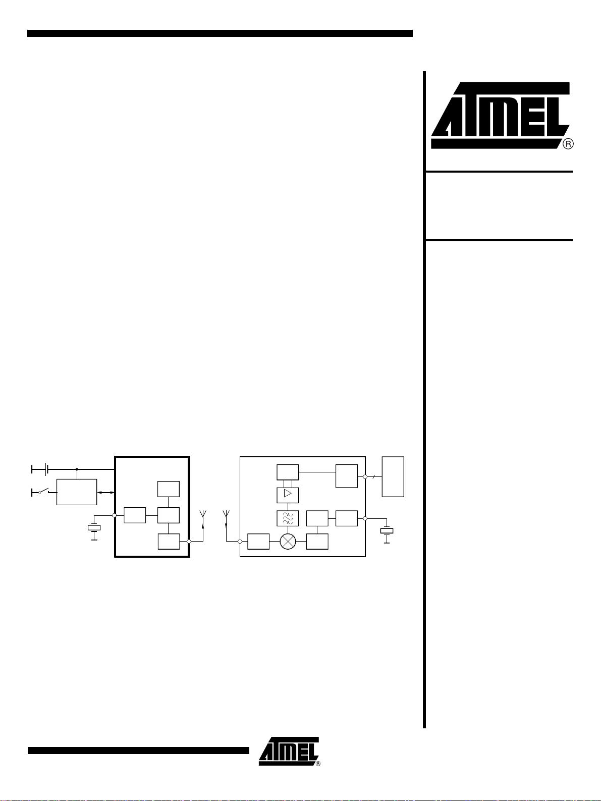
The T5754 is a PLL t ransmitte r IC whic h has been developed for the demands of R F
low-cost transmission systems at data rates up to 32 kBaud. The transmitting
frequency range is 429 MHz to 439 MHz. It can be used in both FSK and ASK
systems.
Figure 1. System Block Diagram
1 Li cell
Keys
Encoder
M44Cx9x
UHF ASK/FSK
Remote control transmitter
T5754
PLL
XTO
VCO
Power
amp.
Antenna Antenna
U3741B/
U3745B/
T5743/
T5744
LNA VCO
UHF ASK/FSK
Remote control receiver
Demod.
IF Amp
PLL XTO
Control
1...3
µC
Preliminary
Rev. 4511D–RKE–08/02
1
Page 2
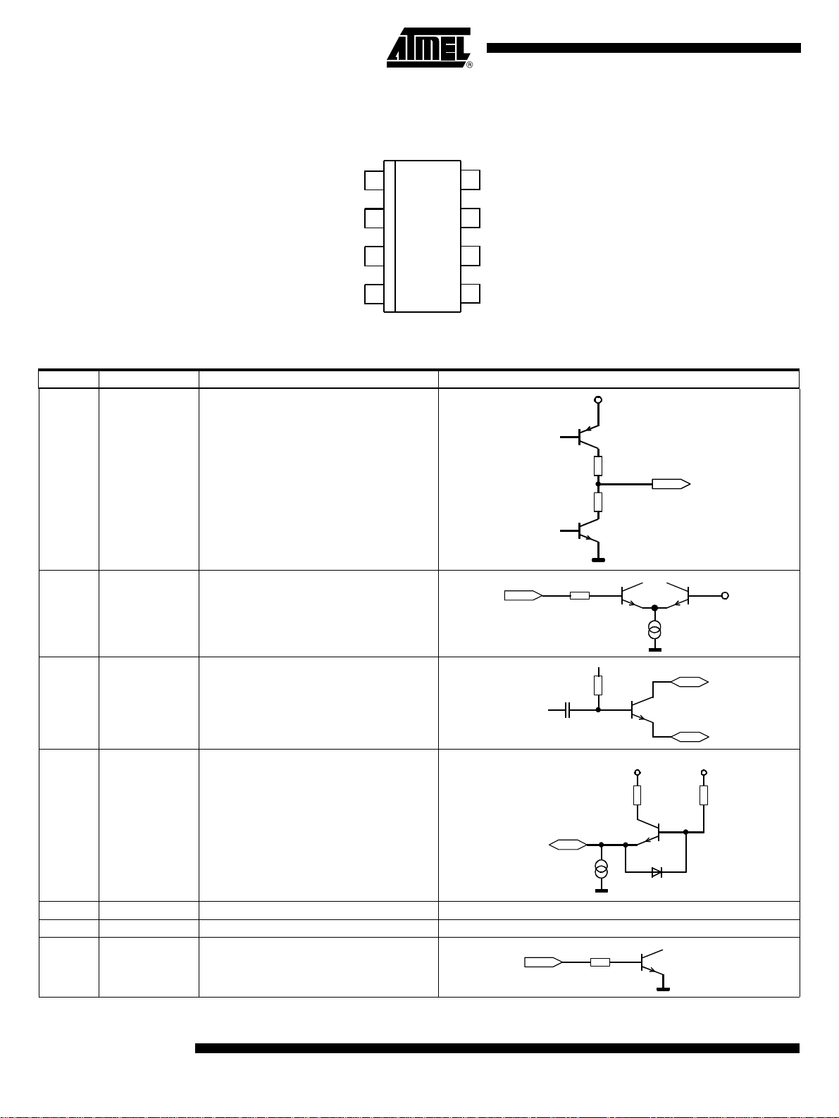
Pin Configuration
Figure 2. Pinning TSSOP8L
CLK
PA_ENABLE
ANT2
ANT1
1
2
T5754
3
4
8
7
6
5
ENABLE
GND
VS
XTAL
Pin Description
Pin Symbol Function Configuration
1 CLK Clock output signal for microconroller
The clock output fre quency is set by the
crystal to f
XTAL
/ 4
2 PA_ENABLE Switches on power amplifier, used for
ASK modulation
PA_ENABLE
VS
100
100
50k
CLK
Uref=1.1V
20 mA
3
4
5 XTAL Connection for crystal
ANT2
ANT1
Emitter of antenna output stage
Open collector antenna output
XTAL
182 mA
1.5k
ANT1
ANT2
VS
1.2k
6 VS Supply voltage See ESD protection circuitry (see Figure 8)
7 GND Ground See ESD protection circuitry (see Figure 8)
8 ENABLE Enable input
ENABLE
200k
VS
2
T5754
4511D–RKE–08/02
Page 3
Figure 3. Block Diagram
CLK
1
T5754
T5754
Power up / down
f
4
f
32
ENABLE
8
PA_ENABLE
ANT2
ANT1
2
3
4 5
PA
PLL
PFD
CP
LF
VCO
XTO
GND
7
VS
6
XTAL
General Desc ription This fully integr ated PLL tran smitter allows particu larly simp le, low-cos t RF miniature
transmitters to be assembled. The VCO is locked to 32 f
is needed for a 433.92 MHz transmitter. All other PLL and VCO peripheral elements are
integrated.
hence a 13.56 MHz crysta l
XTAL
4511D–RKE–08/02
The XTO is a series res onance oscillator so that only one capac itor together with a
crystal connected in series to GND are needed as external elements.
The crystal oscillator together with the PLL needs typically <1 ms until the PLL is locked
and the CLK output is stable. There is a wait time of ³ 1 ms until the CLK is used for the
microcontroller and the PA is switched on.
The power amplifier is an open-collector output delivering a current pulse which is nearly
independent from the load impedance. The delivered output power is hence controllable
via the connected load impedance.
This output configuration enables a simple matching to any kind of antenna or to 50 W. A
high power effici ency of h =P
an optimized load impedance of Z
out
/(I
S,PA VS
Load
) of 36% for the power amplifier results when
= (166 + j223) W is used at 3 V supply voltage.
3
Page 4
Functional
Description
If ENABLE = L and the PA _EN AB LE = L, the circuit is i n s tand by mo de c on su min g o nly
a very small amount of current so that a lithium c ell used as pow er supply can work for
several years.
With ENABLE = H the XTO, PLL and the CLK driver ar e switche d on. If PA _ENABLE
remains L only the PLL and the XTO is running and the CLK signal is delivered to the
microcontroller. The VCO locks to 32 times the XTO frequency.
With ENABLE = H and PA_ENABLE = H the PLL, XT O, CLK driver and the power
amplifier are on. With PA_ENABLE the power amplifier can be switched on and off,
which is used to perform the ASK modulation.
ASK Transmission The T5754 is activated by ENABLE= H. PA_ENABLE must remain L for t ³1ms, then
the CLK signal can be taken to clock the microcontroller and the output power can be
modulated by means of Pin PA_ENABLE. After transmission PA_ENABLE is switched
to L and the microcontroller switches back to internal clocking. The T5754 is switched
back to standby mode with ENABLE = L.
FSK Transmission The T5754 is activated by ENABLE = H. PA_ENABLE must remain L for t ³1ms, then
the CLK signal can be taken to clo ck the microcontroll er and the power amplifie r is
switched on with PA_ENABLE = H. The chip is then ready for FSK modulation. The
microcontroller sta rts to switch on and off the capacit or between the XT AL load cap acitor and GND with an open-drain output port, thus changing the reference frequency of
the PLL. If the switc h is closed , the ou tput frequ ency is lower than if the switc h is ope n.
After transmission PA_ENABLE is switched to L and the microcontroller switches back
to internal clocking. The T5754 is switched back to standby mode with ENABLE = L.
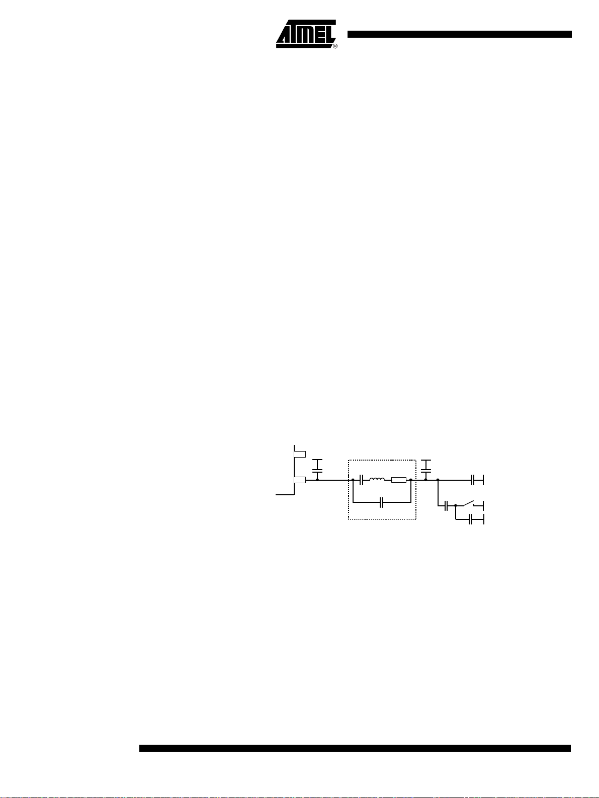
The accuracy of the freq uency dev ia tio n with XT A L pulli ng me tho d is abo ut ±25% when
the following tolerances are considered.
Figure 4. Tolerances of Frequency Modulation
~
V
S
C
Stray1
CMLMR
Crystal equivalent circuit
C
0
Using C
XTAL
~
=9.2pF ±2%, C5=6.8pF ±5%, a switch port with CS
4
capacitances on each side of the crystal of C
capacitance of the crystal of C
=3.2pF ±10% and a crystal with CM=13fF ±10%, an
0
S
Stray1=CStray2
C
Stray2
C
4
C
5
C
Switch
=3pF ±10%, stray
witch
=1pF ±10%, a parallel
FSK deviatio n of ±21 kHz typical with worst case tolerances of ±16.3 kHz to ±28.8 kHz
results.
CLK Output An output CLK signal is provided for a connected microcontroller, the delivered signal is
CMOS compatible if the load capacitance is lower than 10 pF.
Clock Pulse Take-over The clock of the crystal oscillator can be used for clocking the microcontroller. Atmel’s
M4xCx9x has the special feature of starting with an integrated RC-oscillator to switch on
the T5754 with ENABLE = H, and after 1 ms to assume the clock signal of the transmission IC, so that the message can be sent with crystal accuracy.
4
T5754
4511D–RKE–08/02
Page 5

T5754
Output Matching and Power
Setting
The output power is set by the l oad impe dance o f the ante nna. Th e maximum output
power is achieved with a load impeda nce of Z
low resistive path to V
to deliver the DC current.
S
=(166+j223)W. There must be a
Load,opt
The delivered current pulse of the power amplifier is 9 mA and the maximum output
power is del ivered t o a re sistiv e load of 4 65 W if the 1.0 pF ou tput cap acitance of the
power amplifier is compensated by the load impedance.
An optimum load impedance of:
Z
= 465 W || j/(2 ´p1.0 pF) = (166 + j223) W thus r esults for the maximum output
Load
power of 7.5 dBm.
The load impedance is defined as the impedance seen from the T5754’s ANT1, ANT2
into the matching network. Do not confuse this large signal load impedance with a small
signal input impedan ce deliver ed as in put charac teristi c of RF amplifi ers and mea sured
from the application into the IC instead of from the IC into the application for a power
amplifier.
Less output power is achieved by lowering the real parallel part of 465 W where the
parallel imaginary part should be kept constant.
Output power measurement can be do ne wi th the circ uit of F i gure 5. Note tha t the c omponent values mus t be chan ged to com pensat e the indi vidual bo ard par asitics until the
T5754 has the right load impedance Z
=(166+j223)W. Also the damping of the
Load,opt
cable used to measure the output power must be calibrated out.
Figure 5. Output Power Measurement
V
S
C1 = 1n
L
= 33n
~
ANT1
Z
ANT2
~
1
C2 = 2.2p
Lopt
Application Circuit For the supply-voltage blocking capacitor C
(see Figure 6 and Figure 7). C
amplifier where C
for C
two capacitors in series should be used to achieve a better tolerance value and to
2
typically is 8.2 pF/NP0 and C2 is 6 pF/NP0 (10 pF + 15 pF in series);
1
have the possibility to realize the Z
C
forms together with the pins of T5754 and the PCB board wires a series resonance
1
loop that suppresses the 1
Normally the best sup re ssio n is a ch ie ved when C
Pins ANT1 and ANT2.
The loop antenna should not exceed a width of 1.5 mm, otherwise the Q-factor of the
loop antenna is too high.
L
([50 nH to 100 nH) can be pri nted on PCB. C4 should be selec ted tha t the X TO r uns
1
on the load resonance fr equency of the crysta l. Normal ly, a valu e of 12 pF resu lts for a
15 pF load-capacitance crystal.
and C2 are used to match the loop antenna to the power
1
by using standard valued capacitors.
Load,opt
st
harmonic, hence the position of C1 on the PC B i s i mp o rt a nt .
Power
meter
Z = 50 W
R
in
50 W
a value of 68 nF/X7R is recommended
3
is placed as cl os e a s po ss ib le to th e
1
4511D–RKE–08/02
5
Page 6

Figure 6. ASK Application Circuit
S1
S2
PA_ENABLE
BPXY
BPXY
BPXY
OSC1
CLK
7
1
2
M4xCx9x
T5754
VDD
1
VSS
20
BPXY
Power up / down
f
4
ENABLE
8
VS
f
32
GND
7
PFD
C3
C2
ANT2
3
Loop
Antenna
6
T5754
C1
VS
L1
ANT1
4 5
PA
PLL
CP
LF
VCO
XTO
VS
6
XTAL
VS
XTAL
C4
4511D–RKE–08/02
Page 7

Figure 7. FSK Application Circuit
S1
BPXY
M4xCx9x
VDD
1
T5754
VS
S2
PA_ENABLE
BPXY
BPXY
OSC1
CLK
VSS
20
BP42/T2O
18
BPXY
7
T5754
Power up / down
1
f
4
ENABLE
8
f
32
GND
2
PFD
7
4511D–RKE–08/02
Loop
Antenna
C2
C1
VS
L1
ANT2
CP
3
LF
ANT1
4 5
PA
PLL
VCO
XTO
VS
6
XTAL
C3
VS
XTAL
C5
C4
7
Page 8

Figure 8. ESD Protection Circuit
VS
ANT1
CLK PA_ENABLE
GND
ANT2
XTAL ENABLE
Absolute Maximum Ratings
Parameters Symbol Minimum Maximum Unit
Supply voltage V
Power dissipation P
Junction temperature T
Storage temperature T
Ambient temperature T
tot
stg
amb
S
j
-55 125 °C
-55 125 °C
5V
100 mW
150 °C
Thermal Resistance
Parameters Symbol Value Unit
Junction ambient R
thJA
170 K/W
Electrical Characteristics
VS = 2.0 V to 4.0 V, T
Typical values are given at V
Parameters Test Conditions Symbol Min. Typ. Max. Unit
Supply current Power down,
Supply current Power up, PA off, V
Supply current Power up, VS= 3.0 V,
Output power V
8
T5754
= -40°C to 125°C unless otherwise specified.
amb
= 3.0 V and T
S
V
ENABLE
V
PA-ENABLE
V
PA-ENABLE
= 25°C. All parameters are refered to GND (Pin 7).
amb
< 0.25 V, -40°C to 85°C
< 0.25 V, -85°C to +125°C
< 0.25 V, 25°C
(100% correlation tested)
= 3 V,
amb
S
PA-ENABL E
PA-ENABL E
=25°C,
= (166 + j233) W
Load
<0.25V
>1.7V
ENABLE
ENABLE
= 3.0 V, T
S
> 1.7 V, V
> 1.7 V, V
V
V
f = 433.92 MHz, Z
I
S_Off
I
S
I
S_T r ansmit
P
Ref
350
7
<10
3.7 4.8 mA
911.6mA
5.5 7.5 10 dBm
4511D–RKE–08/02
nA
µA
nA
Page 9

Electrical Characteristics (Continued)
T5754
VS = 2.0 V to 4.0 V, T
Typical values are given at V
= -40°C to 125°C unless otherwise specified.
amb
= 3.0 V and T
S
= 25°C. All parameters are refered to GND (Pin 7).
amb
Parameters Test Conditions Symbol Min. Typ. Max. Unit
Output power v ariation for the full
temperature range
Output power v ariation for the full
temperature range
Achievable output-power range Selectable by load impedance P
Spurious emission f
T
= -40°C to +85°C,
amb
V
= 3.0 V
S
= 2.0 V
V
S
= -40°C to +125°C,
T
amb
V
= 3.0 V
S
= 2.0 V,
V
S
= P
P
Out
CLK
Ref
= f0/128
+ DP
Ref
DP
Ref
DP
Ref
DP
Ref
DP
Ref
Out_typ
-1.5
-4.0
-2.0
-4.5
dB
dB
dB
dB
07.5dBm
Load capacitance at Pin CLK = 10 pF
fO ± 1´ f
± 4 ´ f
f
O
CLK
CLK
-55
-52
dBc
dBc
other spurious are lower
Oscillator frequency XTO
(= phase comparator frequency)
= f0/32
f
XTO
= resonant frequency of the
f
XTAL
XTAL, C
£ 10 fF, load capacitance
M
selected accordingly
T
= -40°C to +85°C,
amb
= -40°C to +125°C
T
amb
f
XTO
-30
-40
f
XTAL
+30
+40
ppm
ppm
PLL loop bandwidth 250 kHz
Phase noise of phase
comparator
Referred to f
25 kHz distance to carrier
PC
= f
XT0,
-116 -110 dBc/Hz
In loop phase noise PLL 25 kHz distance to carrier -86 -80 dBc/Hz
Phase noise VCO at 1 MHz
at 36 MHz
Frequency range of VCO f
Clock output frequen cy (CMOS
microcontroller compatible)
Voltage swing at Pin CLK C
£ 10 pF V
Load
VCO
0h
V
429 439 MHz
VS´ 0.8
0l
-94
-125
/128 MHz
f
0
V
-90
-121
´ 0.2
S
dBc/Hz
dBc/Hz
V
V
Series resonance R of the c rystal Rs 110 W
Capaictive load at Pin XT0 7pF
FSK modulation frequency rate Duty cycle of the modulation signal =
50%
ASK modulation frequency rate Duty cycle of the modulation signal =
50%
ENABLE input Low level input voltage
High level input voltage
Input current high
PA_E NABLE input Low level input voltage
High level input voltage
Input current high
V
Il
V
Ih
I
In
V
Il
V
Ih
I
In
032kHz
032kHz
0.25
1.7
20
0.25
1.7
5
V
V
mA
V
V
mA
4511D–RKE–08/02
9
Page 10

Ordering Information
Extended Type Numb er Package Remarks
T5754-6AQ TSSOP8L Taped and reeled
Package Information
10
T5754
4511D–RKE–08/02
Page 11

Atmel Headquar ters Atmel Operations
Corporate Headquarters
2325 Orchard Parkway
San Jose, CA 95131
TEL 1(408) 441-0311
FAX 1(408) 487-2600
Europe
Atmel Sarl
Route des Arsenaux 41
Case Postale 80
CH-1705 Fribourg
Switzerland
TEL (41) 26-426-5555
FAX (41) 26-426-5500
Asia
Room 1219
Chinachem Gol den P laza
77 Mody Road Tsimhatsui
East Kowloon
Hong Kong
TEL (852) 2721-9778
FAX (852) 2722-1369
Japan
9F, Tonetsu Shinkawa Bldg.
1-24-8 Shin kawa
Chuo-ku, Tokyo 104-0033
Japan
TEL (81) 3- 3523-3 551
FAX (81) 3-3523-7581
Memory
2325 Orchard Parkway
San Jose, CA 95131
TEL 1(408) 441-0311
FAX 1(408) 436-4314
Microcontrollers
2325 Orchard Parkway
San Jose, CA 95131
TEL 1(408) 441-0311
FAX 1(408) 436-4314
La Chantrerie
BP 70602
44306 Nantes Cedex 3, France
TEL (33) 2-40-18-18-18
FAX (33) 2- 40-18- 19-6 0
ASIC/ASSP/Smart Cards
Zone Industrielle
13106 Rousset Cedex, France
TEL (33) 4-42-53-60-00
FAX (33) 4- 42-53- 60-0 1
1150 East Cheyenne Mtn. Blvd.
Colorado Springs, CO 80906
TEL 1(719) 576-3300
FAX 1(719) 540-1759
Scottish Enterprise Technology Park
Maxwell Building
East Kilbride G75 0QR, Scotland
TEL (44) 1355-803-000
FAX (44) 1355-242-743
RF/Automotive
Theresienstrasse 2
Postfach 3535
74025 Heilbro nn, Ge rmany
TEL (49) 71-31-67-0
FAX (49) 71-31-67-2340
1150 East Cheyenne Mtn. Blvd.
Colorado Springs, CO 80906
TEL 1(719) 576-3300
FAX 1(719) 540-1759
Biometrics/Imaging/Hi-Rel MPU/
High Speed Converters/RF Datacom
Avenue de Rochepleine
BP 123
38521 Saint-Egreve Cedex, France
TEL (33) 4-76-58-30-00
FAX (33) 4- 76-58- 34-8 0
e-mail
literature@atmel.com
Web Site
http://www.atmel.com
© Atmel Corporation 2002.
Atmel Corporation makes no warranty for the use of its products, other than those expressly contained in the Company’s standard warranty
which is detailed in Atmel’s Terms and Conditions located on the Company’s web site. The Company assumes no responsibility for any errors
which may appear in this document, reserves the right to change devices or specifications det ailed herein at any time without notice, and does
not make any commitment to update the information contained herein. No licenses to patents or other intellectual property of Atmel are granted
by the Company in connection with the sale of Atmel products, expressly or by implication. Atmel’s products are not authorized for use as critical
components in life support devices or systems.
Atmel® is the registered trademark of Atmel.
Other terms and product names may be the trademarks of others.
Printed on recycled paper.
4511D–RKE–08/02
xM
 Loading...