

Page 1
Features
• Minimal External Circuitry Requirements, no RF Components on the PC Board Except
Matching to the Receiver Antenna
• High Sensitivity, Especially at Low Data Rates
• SSO20 and SO20 package
• Fully Integrated VCO
• Supply Voltage 4.5 V to 5.5 V, Operating Temperature Range -40°C to 105°C
• Single-ended RF Input for Easy Adaptation to l/4 Antenna or Printed Antenna on PCB
• Low-cost Solution Due to High Integration Level
• Various Types of Protocols Supported (i.e., PWM, Manchester and Biphase)
• Distinguishes the Signal Strength of Several Transmitters via RSSI (Received Signal
Strength Indicator)
• ESD Protection According to MIL-STD. 883 (4KV HBM)
• High Image Frequency Suppression Due to 1 MHz IF in Conjunction with a SAW Front-
end Filter, up to 40 dB is thereby Achievable with Newer SAWs
• Power Management (Polling) is Possible by Means of a Separate Pin via the
Microcontroller
• Receiving Bandwidth BIF = 600 kHz
UHF ASK
Receiver
T5744
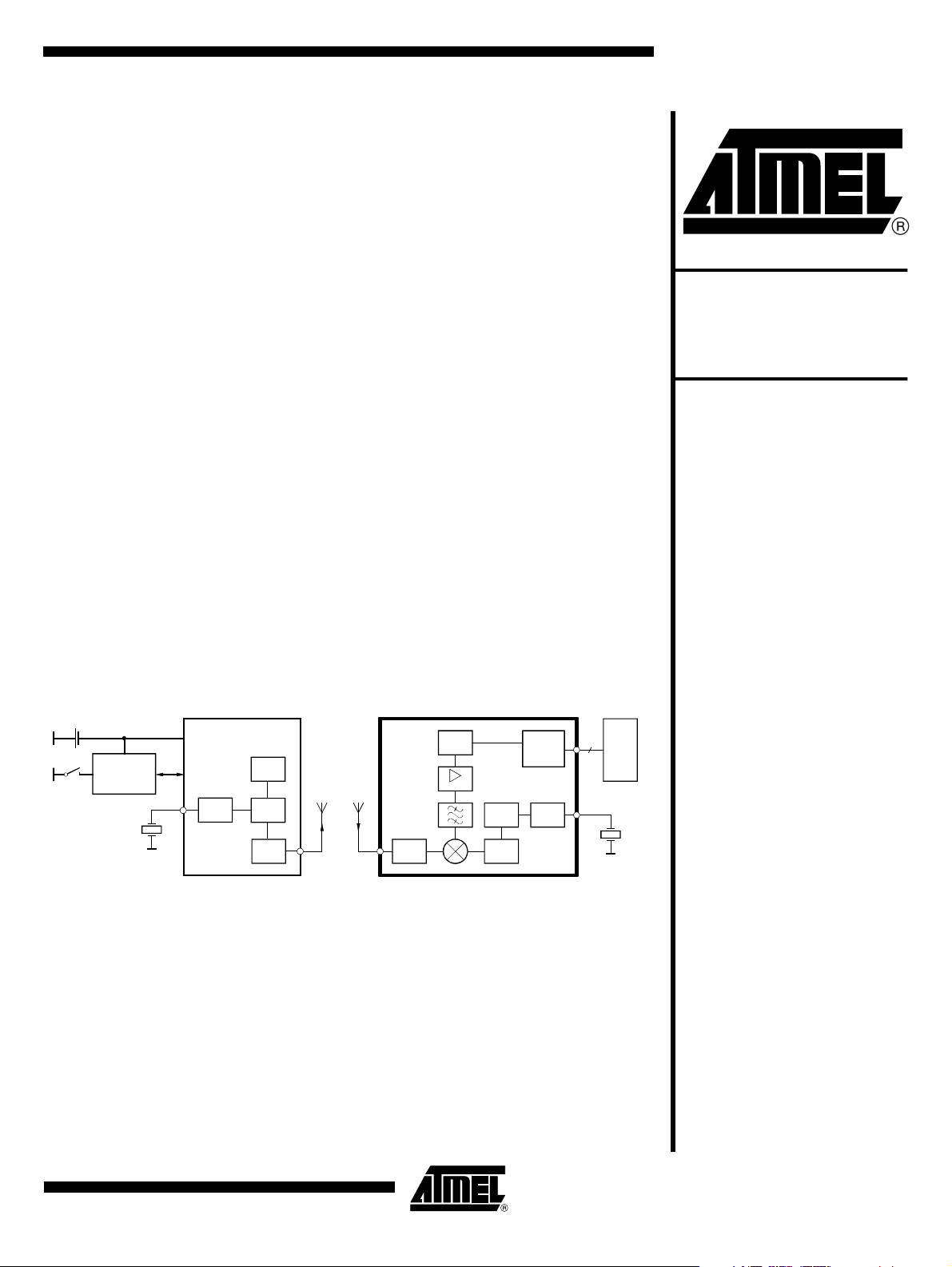
Description
The T5744 is a PLL receiver device for the receiving range of f0= 300 MHz to
450 MHz. It is developed for the demands of RF low-cost data communication systems with low data rates and fits for most types of modulation schemes including
Manchester, Biphase and most PWM protocols. Its main applications are in the areas
of telemetering, security technology and keyless-entry systems.
Figure 1. System Block Diagram
1 Li cell
Keys
Encoder
M44Cx9x
UHF ASK/FSK
Remote control transmitter
U2741B
PLL
XTO
VCO
Power
amp.
T5744
Antenna Antenna
LNA VCO
UHF ASK
Remote control receiver
Demod.
IF Amp
PLL XTO
Data
interface
1...3
µC
Preliminary
Rev. 4521A–RKE–02/02
1
Page 2
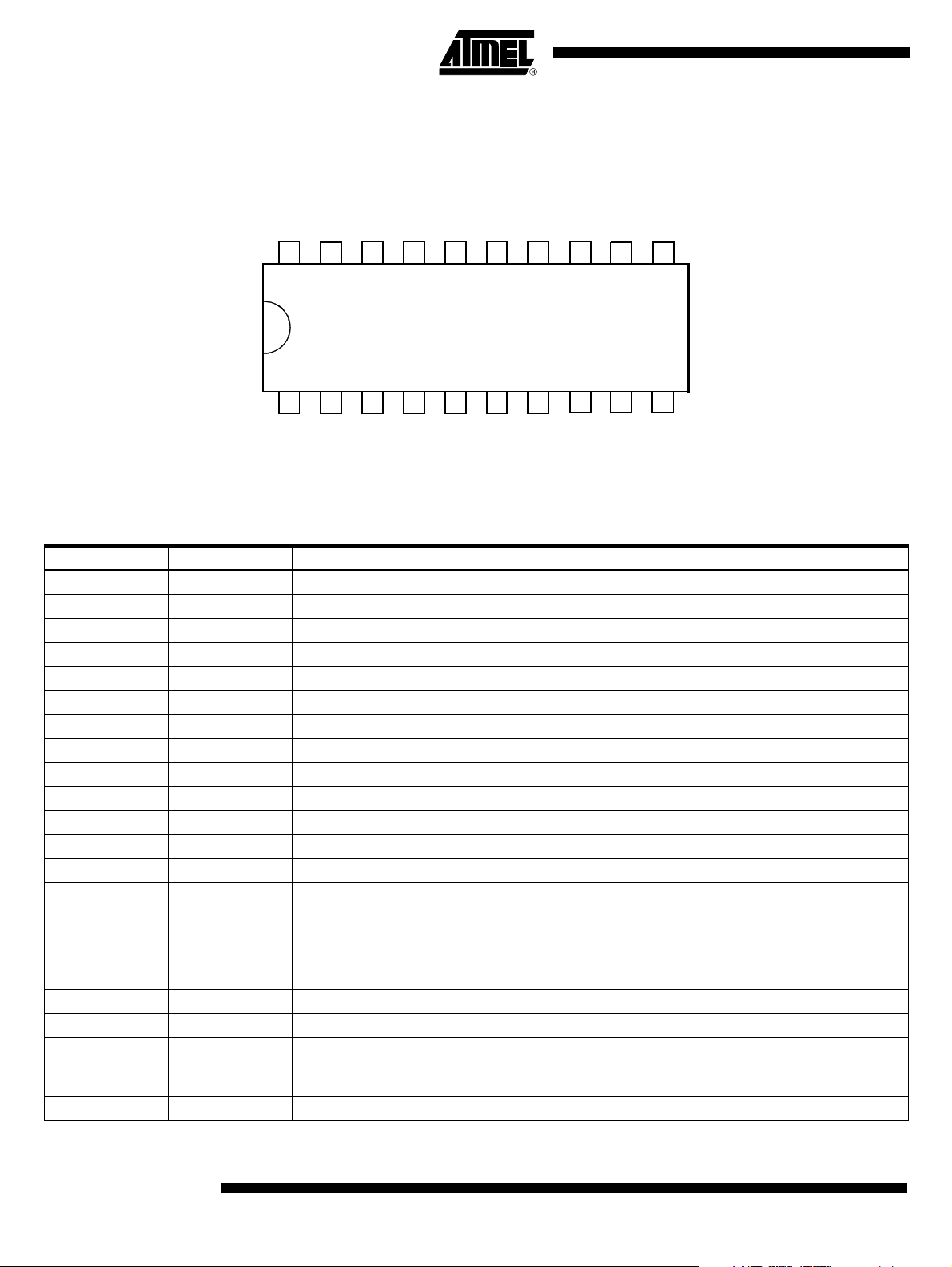
Pin Configuration
Figure 2. Pinning SO20 and SSO20
Pin Description
Pin Symbol Function
1 BR_0 Baud rate select LSB
2 BR_1 Baud rate select MSB
3 CDEM Lower cut-off frequency data filter
4 AVCC Analog power supply
5 AGND Analog ground
6 DGND Digital ground
7 MIXVCC Power supply mixer
8 LNAGND High-frequency ground LNA and mixer
9LNA_INRF input
10 n.c. Not connected
11 LFVCC Power supply VCO
12 LF Loop filter
13 LFGND Ground VCO
14 XTO Crystal oscillator
15 DVCC Digital power supply
16 MODE
17 RSSI Output of the RSSI amplifier
18 TEST Test pin, during operation at GND
19 ENABLE
20 DATA Data output
DATA
20
19
2
1
BR_1
BR_0
RSSI
MODE
18
3
CDEM
16
17
4
5
AVCC
AGND
TEST
ENABLE
Selecting 433.92 MHz /315 MHz
Low: 315 MHz (USA)
High: 433.92 MHz (Europe)
Selecting operation mode
Low: sleep mode
High: receiving mode
DVCC
T5744
6
DGND
XTO
141513
7
MIXVCC
LF
LFGND
8
LNAGND
LFVCC
12
11
9
10
n.c.
LNA_IN
2
T5744
4521A–RKE–02/02
Page 3
Figure 3. Block Diagram
T5744
BR_0 BR_1
CDEM
RSSI
AVCC
AGND
DGND
MIXVCC
LNAGND
LNA_IN
LNA
ASK-
Demodulator
and data filter
RSSI
RSSI IF Amp
4. Order
LPF
3 MHz
IF Amp
LPF
3 MHz
Dem_out
Data interface
Test
Standby logic
VCO XTO
f
64
DATA
TEST
MODE
DVCC
ENABLE
LFGND
LFVCC
XTO
LF
RF Front End The RF front end of the receiver is a heterodyne configuration that converts the input
signal into a 1-MHz IF signal. According to Figure 3, the front end consists of an LNA
(Low-Noise Amplifier), LO (Local Oscillator), a mixer and RF amplifier.
The LO generates the carrier frequency for the mixer via a PLL synthesizer. The XTO
. The VCO (Voltage-Controlled
XTO
for the mixer. fLO is dependent on
LO
LO
XTO
/64 is
and
4521A–RKE–02/02
(crystal oscillator) generates the reference frequency f
Oscillator) generates the drive voltage frequency f
the voltage at Pin LF. f
by the phase frequency detector. The current output of the phase frequency detec-
f
XTO
is divided by factor 64. The divided frequency is compared to
LO
tor is connected to a passive loop filter and thereby generates the control voltage VLF
for the VCO. By means of that configuration, VLF is controlled in a way that f
equal to f
f
XTO
. If fLO is determined, f
XTO
= fLO/64
can be calculated using the following formula:
XTO
The XTO is a one-pin oscillator that operates at the series resonance of the quartz crystal. According to Figure 4, the crystal should be connected to GND via a capacitor CL.
The value of that capacitor is recommended by the crystal supplier. The value of CL
should be optimized for the individual board layout to achieve the exact value of f
hereby of f
. When designing the system in terms of receiving bandwidth, the accuracy
LO
of the crystal and the XTO must be considered.
3
Page 4
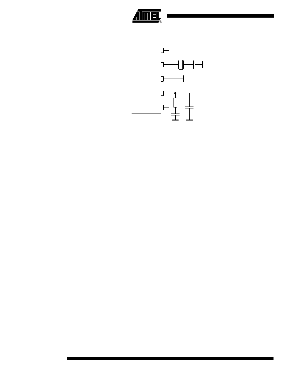
Figure 4. PLL Peripherals
DVCC
XTO
V
S
C
L
LFGND
R1 = 820 Ω
C9 = 4.7 nF
LF
LFVCC
R1
V
S
C9
C10 = 1 nF
C10
The passive loop filter connected to Pin LF is designed for a loop bandwidth of BLoop =
100 kHz. This value for BLoop exhibits the best possible noise performance of the LO.
Figure 4 shows the appropriate loop filter components to achieve the desired loop
bandwidth
is determined by the RF input frequency fRF and the IF frequency fIF using the follow-
f
LO
ing formula:
= fRF - f
f
LO
IF
To determine fLO, the construction of the IF filter must be considered at this point. The
nominal IF frequency is f
quencies, the filter is tuned by the crystal frequency f
fixed relation between f
= 1 MHz. To achieve a good accuracy of the filter’s corner fre-
IF
and fLO that depends on the logic level at pin mode. This is
IF
. This means that there is a
XTO
described by the following formulas:
MODE = 0 USA f
MODE = 1 Europe f
The relation is designed to achieve the nominal IF frequency of f
applications. For applications where f
case of f
= 433.92 MHz, MODE must be set to ’1’. For other RF frequencies, fIF is
RF
not equal to 1 MHz. f
= fLO/314
IF
= fLO/432.92
IF
= 1 MHz for most
= 315 MHz, MODE must be set to ’0’. In the
RF
is then dependent on the logical level at Pin MODE and on fRF.
IF
IF
Table 1 summarizes the different conditions.
The RF input either from an antenna or from a generator must be transformed to the RF
input Pin LNA_IN. The input impedance of that pin is provided in the electrical parameters. The parasitic board inductances and capacitances also influence the input
matching. The RF receiver T5744 exhibits its highest sensitivity at the best signal-tonoise ratio in the LNA. Hence, noise matching is the best choice for designing the transformation network.
A good practice when designing the network, is to start with power matching. From that
starting point, the values of the components can be varied to some extent to achieve the
best sensitivity.
If a SAW is implemented into the input network a mirror frequency suppression of
∆P
= 40 dB can be achieved. There are SAWs available that exhibit a notch at
Ref
∆f = 2 MHz. These SAWs work best for an intermediate frequency of IF = 1 MHz. The
selectivity of the receiver is also improved by using a SAW. In typical automotive applications, a SAW is used.
4
T5744
4521A–RKE–02/02
Page 5
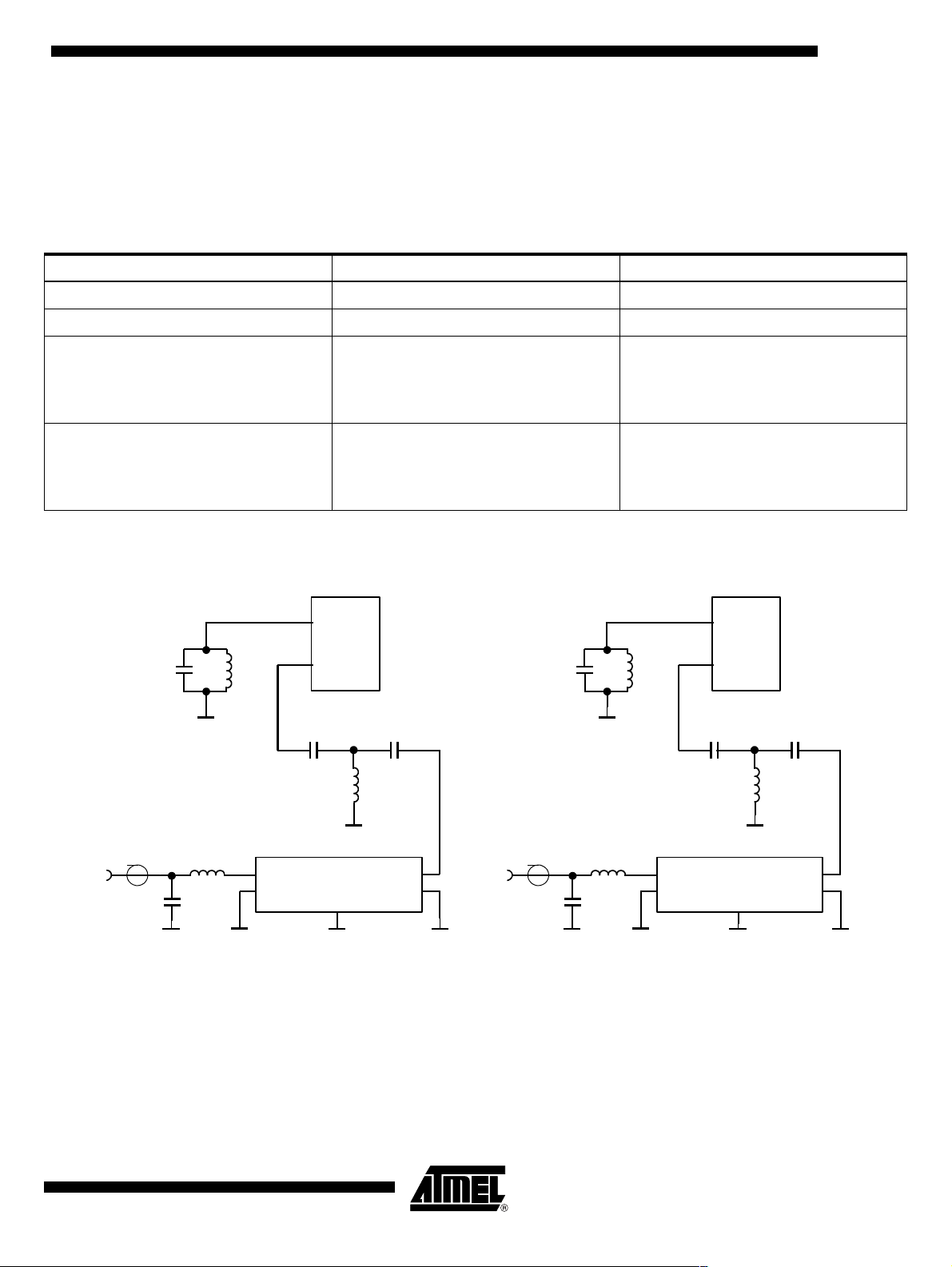
Figure 5 shows a typical input matching network for fRF = 315 MHz and fRF =
433.92 MHz using a SAW. Figure 6 illustrates the input matching to 50
SAW. The input matching networks shown in Figure 6 are the reference networks for the
parameters given in the electrical characteristics.
Table 1. Calculation of LO and IF Frequency
Conditions Local Oscillator Frequency Intermediate Frequency
= 315 MHz, MODE = 0 fLO = 314 MHz fIF = 1 MHz
f
RF
f
= 433.92 MHz, MODE = 1 fLO = 432.92 MHz fIF = 1 MHz
RF
T5744
Ω without a
300 MHz < f
365 MHz < f
< 365 MHz, MODE = 0
RF
< 450 MHz, MODE = 1
RF
f
LO
f
LO
Figure 5. Input Matching Network with SAW Filter
8
LNAGND
T5744
C3
22p
fRF = 433.92 MHz
L
25n
9
C16
100p
LNA_IN
L3
27n
C17
8.2p
TOKO LL2012
F27NJ
f
RF
-------------------= f
1
1
--------- -+
314
f
RF
--------------------------- -= f
1
1
----------------- -+
432.92
C3
47p
L
25n
fRF = 315 MHz
f
RF
--------- -=
IF
314
f
RF
----------------- -=
IF
432.92
8
LNAGND
T5744
9
LNA_IN
C16
100p
L3
47n
C17
22p
TOKO LL2012
F47NJ
RF
IN
4521A–RKE–02/02
C2
8.2p
L2
TOKO LL2012
F33NJ
33n
1
2
IN
IN_GND
B3555
CASE_GND
3,4 7,8
OUT
OUT_GND
L2
C2
10p
TOKO LL2012
F82NJ
82n
1
2
IN
IN_GND
B3551
CASE_GND
3,4 7,8
OUT
OUT_GND
5
6
RF
5
6
IN
5
Page 6
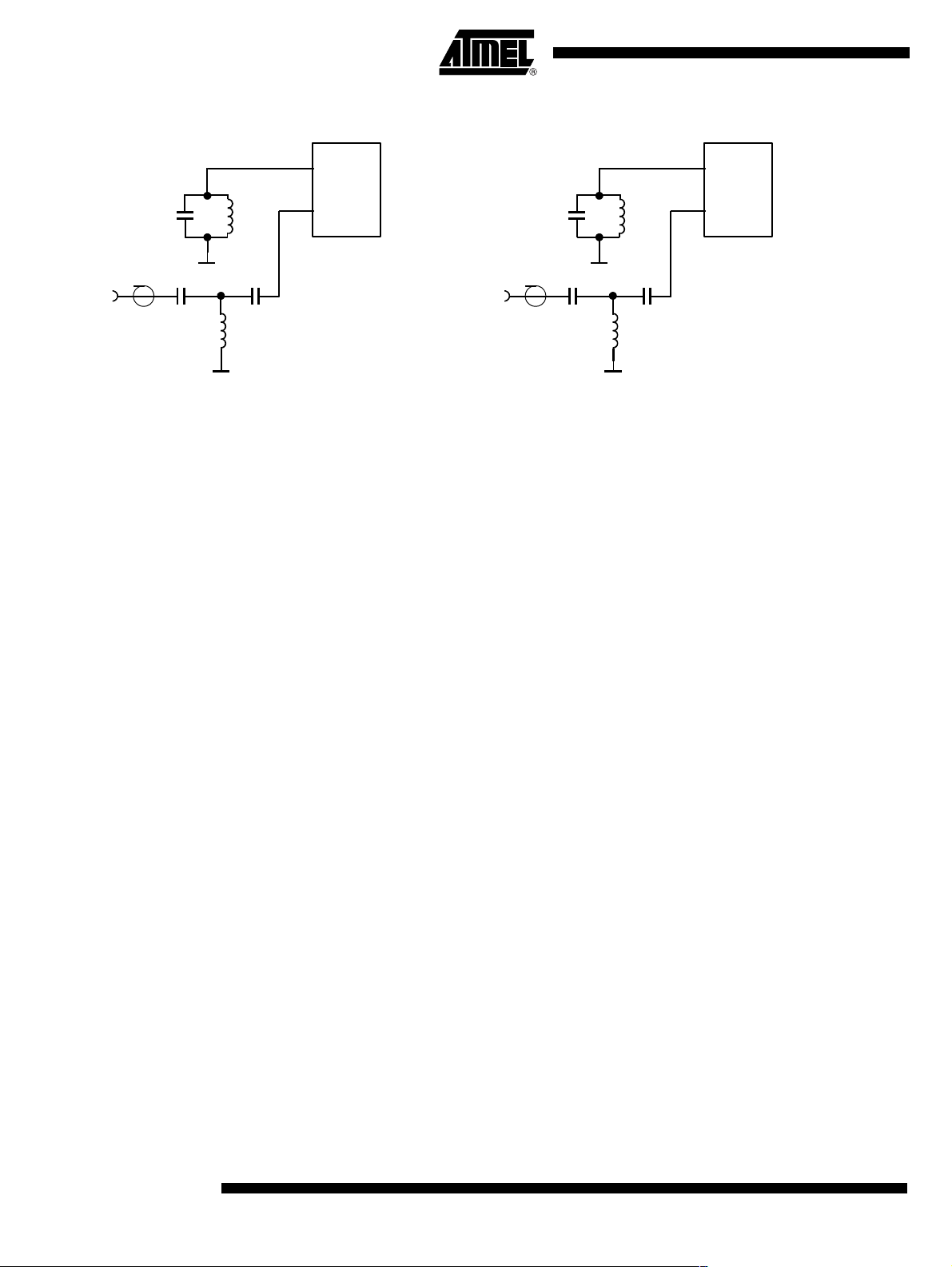
Figure 6. Input Matching Network without SAW Filter
fRF = 433.92 MHz
C3
15p
RF
IN
3.3p
22n
25n
100p
TOKO LL2012
F22NJ
8
9
Please note that for all coupling conditions (see Figure 5 and Figure 6), the bond wire
inductivity of the LNA ground is compensated. C3 forms a series resonance circuit
together with the bond wire. L = 25 nH is a feed inductor to establish a DC path. Its value
is not critical but must be large enough not to detune the series resonance circuit. For
cost reduction, this inductor can be easily printed on the PCB. This configuration
improves the sensitivity of the receiver by about 1 dB to 2 dB.
Analog Signal Processing
LNAGND
T5744
LNA_IN
fRF = 315 MHz
C3
33p
RF
IN
3.3p
39n
25n
100p
TOKO LL2012
F39NJ
8
9
LNAGND
T5744
LNA_IN
IF Amplifier The signals coming from the RF front end are filtered by the fully integrated 4th-order IF
filter. The IF center frequency is f
= 433.92 MHz is used. For other RF input frequencies, refer to Table 1 to determine
f
RF
the center frequency.
The receiver T5744 employs an IF bandwidth of B
together with the U2741B in ASK mode.
= 1 MHz for applications where fRF = 315 MHz or
IF
= 600 kHz and can be used
IF
RSSI Amplifier The subsequent RSSI amplifier enhances the output signal of the IF amplifier before it is
fed into the demodulator. The dynamic range of this amplifier is DRRSSI = 60 dB. If the
RSSI amplifier is operated within its linear range, the best S/N ratio is maintained. If the
dynamic range is exceeded by the transmitter signal, the S/N ratio is defined by the ratio
of the maximum RSSI output voltage and the RSSI output voltage due to a disturber.
The dynamic range of the RSSI amplifier is exceeded if the RF input signal is about
60 dB higher compared to the RF input signal at full sensitivity.
Pin RSSI The output voltage of the RSSI amplifier (VRSSI) is available at Pin RSSI. Using the
RSSI output signal, the signal strength of different transmitters can be distinguished.
The usable input power range P
Since different RF input networks may exhibit slightly different values for the LNA gain,
the sensitivity values given in the electrical characteristics refer to a specific input
matching. This matching is illustrated in Figure 6 and exhibits the best possible
sensitivity.
is -100 dBm to -55 dBm.
Ref
6
T5744
4521A–RKE–02/02
Page 7

Figure 7. RSSI Characteristics
3.0
2.8
2.6
2.4
2.2
(V)
2.0
RRSI
1.8
V
1.6
1.4
1.2
1.0
-130.0 -110.0 -90.0 -70.0 -50.0 -30.0
105°C
25°C
T5744
max.
T
= 40°C
amb
min.
P
(dBm)
Ref
ASK Demodulator and
Data Filter
The signal coming from the RSSI amplifier is converted into the raw data signal by the
ASK demodulator.
An automatic threshold control circuit (ATC) is employed to set the detection reference
voltage to a value where a good signal-to-noise ratio is achieved. This circuit also
implies the effective suppression of any kind of inband noise signals or competing transmitters. If the S/N ratio exceeds 10 dB, the data signal can be detected properly.
The output signal of the demodulator is filtered by the data filter before it is fed into the
digital signal processing circuit. The data filter improves the S/N ratio as its passband
can be adopted to the characteristics of the data signal. The data filter consists of a 1storder highpass and a 1st-order lowpass filter.
The highpass filter cut-off frequency is defined by an external capacitor connected to Pin
CDEM. The cut-off frequency of the highpass filter is defined by the following formula:
fcu_DF
--------------------------------------------------=
2
1
π R1× CDEM××
Recommended values for CDEM are given in the electrical characteristics.
The cut-off frequency of the lowpass filter is defined by the selected baudrate range
(BR_Range). BR_Range is defined by the Pins BR_0 and BR_1. BR_Range must be
set in accordance to the used baudrate.
BR_1 BR_0 BR_Range
000
4521A–RKE–02/02
011
102
112
Each BR_Range is defined by a minimum and a maximum edge-to-edge time (tee_sig).
These limits are defined in the electrical characteristics. They should not be exceeded to
maintain full sensitivity of the receiver.
7
Page 8

Receiving
Characteristics
The RF receiver T5744 can be operated with and without a SAW front-end filter. In a
typical automotive application, a SAW filter is used to achieve better selectivity. The
selectivity with and without a SAW front-end filter is illustrated in Figure 7. Note that the
mirror frequency is reduced by 40 dB. The plots are printed relatively to the maximum
sensitivity. If a SAW filter is used, an insertion loss of about 4 dB must be considered.
When designing the system in terms of receiving bandwidth, the LO deviation must be
considered as it also determines the IF center frequency. The total LO deviation is calculated to be the sum of the deviation of the crystal and the XTO deviation of the T5744.
Low-cost crystals are specified to be within ±100 ppm. The XTO deviation of the T5744
is an additional deviation due to the XTO circuit. This deviation is specified to be
±30 ppm. If a crystal of ±100 ppm is used, the total deviation is ±130 ppm in that case.
Note that the receiving bandwidth and the IF-filter bandwidth are equivalent.
Figure 8. Receiving Frequency Response
Basic Clock Cycle of the
Digital Circuitry
0.0
-20.0
-40.0
-60.0
dP (dB)
-80.0
-100.0
-6.0 -5.0 -4.0 -3.0 -2.0 -1.0 0.0 1.0 2.0 3.0 4.0 5.0 6.0
df (MHz)
without SAW
with SAW
The complete timing of the digital circuitry and the analog filtering is derived from one
clock. According to Figure 9, this clock cycle TClk is derived from the crystal oscillator
(XTO) in combination with a divider. The division factor is controlled by the logical state
at Pin MODE. According to chapter 'RF Front End', the frequency of the crystal oscillator
) is defined by the RF input signal (f
(f
XTO
of the local oscillator (f
LO
).
) which also defines the operating frequency
RFin
Figure 9. Generation of the Basic Clock Cycle
T
Clk
Divider
:14/:10
MODE
16
L : USA(:10)
H: Europe(:14)
f
XTO
XTO
8
T5744
DVCC
15
XTO
14
4521A–RKE–02/02
Page 9

T5744
Pin MODE can now be set in accordance with the desired clock cycle T
Clk
. T
controls
Clk
the following application-relevant parameters:
Timing of the analog and digital signal processing
IF filter center frequency (f
Most applications are dominated by two transmission frequencies: f
mainly used in USA, f
Send
)
IF0
= 315 MHz is
Send
= 433.92 MHz in Europe. In order to ease the usage of all T
Clk
dependent parameters, the electrical characteristics display three conditions for each
parameter.
• Application USA
= 4.90625 MHz, MODE = L, T
(f
XTO
= 2.0383 µs)
Clk
• Application Europe
= 6.76438 MHz, MODE = H, T
(f
XTO
= 2.0697 µs)
Clk
• Other applications
is dependent on f
(T
Clk
characteristic is given as a function of T
and on the logical state of Pin MODE. The electrical
XTO
Clk
).
The clock cycle of some function blocks depends on the selected baud rate range
(BR_Range) which is defined by the Pins BR_0 and BR_1. This clock cycle T
XClk
is
defined by the following formulas for further reference:
BR_Range = BR_Range0: T
BR_Range1: T
BR_Range2: T
BR_Range3: T
XClk
XClk
XClk
XClk
= 8 × T
= 4 × T
= 2 × T
= 1 × T
Clk
Clk
Clk
Clk
-
Pin ENABLE Via the Pin ENABLE the operating mode of the receiver can be selected (see Figure 10
and Figure 11).
If the Pin ENABLE is held to Low, the receiver remains in sleep mode. All circuits for sig-
nal processing are disabled and only the XTO is running in that case. The current
= I
consumption is I
S
to a transmitter signal.
To activate the receiver, the Pin ENABLE must be held to High. During the start-up
period, T
, all signal processing circuits are enabled and settled. The duration of the
Startup
start-up period depends on the selected baud-rate range (BR_Range).
After the start-up period, all circuits are in a stable condition and the receiver is in the
receiving mode.
In receiving mode, the internal data signal (Dem_out) is switched to Pin DATA. To avoid
incorrect timing at the begin of the data stream, the begin is synchronized to a falling
edge of the incoming data signal. The receiver stays in the receiving mode until it is
switched back to sleep mode via Pin ENABLE.
During start-up and receiving mode, the current consumption is I
in that case. During the sleep mode the receiver is not sensitive
Soff
= I
Son
.
S
4521A–RKE–02/02
9
Page 10

Figure 10. Enable Timing (1)
Dem_out
ENABLE
DATA
Figure 11. Enable Timing (2)
Dem_out
ENABLE
Sleep mode Start-up mode Receiving mode
I
S
= I
Soff
I
S
T
= I
Start-up
Son
I
= I
S
Son
t
ee_sig
t
ee_sig
DATA
Digital Signal
Processing
Sleep mode Start-up mode Receiving mode
I
= I
S
Soff
I
S
T
= I
Son
Start-up
I
= I
S
Son
The data from the ASK demodulator (Dem_out) is digitally processed in different ways
and as a result converted into the output signal DATA. This processing depends on the
selected baudrate range (BR_Range). Figure 12 illustrates how Dem_out is synchronized by the extended basic clock cycle T
. Data can change its state only after T
XClk
has elapsed. The edge-to-edge time period tee_sig of the DATA signal as a result is
always an integral multiple of T
XClk
.
The minimum time period between two edges of the data signal is limited to tee_sig
TDATA_min. This implies an efficient suppression of spikes at the DATA output. At the
same time it limits the maximum frequency of edges at DATA. This eases the interrupt
handling of a connected microcontroller.
XClk
≥
10
T5744
4521A–RKE–02/02
Page 11

Figure 12. Synchronization of the Demodulator Output
T
XClk
Dem_out
T5744
Data_out (DATA)
t
ee_sig
Figure 13. Debouncing of the Demodulator Output
Dem_out
DATA
t
DATA_min
t
ee
t
DATA_min
t
DATA_min
t
ee
t
ee
Absolute Maximum Ratings
Parameters Symbol Min. Max. Unit
Supply voltage V
Power dissipation P
Juntion temperature T
Storage temperature T
Ambient temperature T
Maximum input level, input matched to 50 Ω P
in_max
tot
stg
amb
S
j
-55 +125 °C
-40 +105 °C
6V
450 mW
150 °C
10 dBm
Thermal Resistance
Parameters Symbol Value Unit
Junction ambient SO20 package R
Junction ambient SSO20 package R
4521A–RKE–02/02
thJA
thJA
100 K/W
100 K/W
11
Page 12

Electrical Characteristics
All parameters refer to GND, T
wise specified. (V
Parameters
= 5 V, T
S
Test Conditions
amb
= 25°C)
amb
Basic Clock Cycle of the Digital Circuitry
Basic clock
cycle
Extended basic
clock cycle
MODE = 0 (USA)
MODE = 1 (Europe)
BR_Range0
BR_Range1
BR_Range2
BR_Range3
Start-up time
(see Figure 10
and Figure 11)
BR_Range0
BR_Range1
BR_Range2
BR_Range3
Receiving Mode
Intermediate
frequency
Minimum time
period between
edges at
Pin DATA
MODE=0 (USA)
MODE=1 (Europe)
BR_Range0
BR_Range1
BR_Range2
BR_Range3
(Figure 13)
Edge to edge
time period of
the data signal
for full
sensitivity
BR_Range0
BR_Range1
BR_Range2
BR_Range3
(Figure 10)
= -40°C to +105°C, VS = 4.5 V to 5.5 V, f0 = 433.92 MHz and f0 = 315 MHz, unless other-
Symbol
T
Clk
T
XClk
T
Startup
f
IF
T
DATA_min
t
ee_sig
6.76438 MHz Osc.
(MODE:1)
Min. Typ. Max. Min. Typ. Max. Min. Typ. Max.
2.0697 2.0697
16.6
8.3
4.1
2.1
1855
1061
1061
663
1.0
165
83
41.4
20.7
400
200
100
50
16.6
8.3
4.1
2.1
1855
1061
1061
663
165
83
41.4
20.7
8479
8479
8479
8479
4.90625 MHz Osc.
(MODE:0)
2.0383 2.0383 1/(f
1/(f
16.3
8.2
4.1
2.0
1827
1045
1045
653
1.0
163
81
40.7
20.4
400
200
100
50
16.3
8.2
4.1
2.0
1827
1045
1045
653
163
81
40.7
20.4
8350
8350
8350
8350
BR_Range
×
2 µs/T
Variable Oscillator
/10)
xto
/14)
xto
× T
8
Clk
4 × T
Clk
2 × T
Clk
1 × T
Clk
896.5
512.5
512.5
320.5
× T
Clk
f
XTO
× 64 / 432.92
f
XTO
10 ´ T
XClk
10 ´ T
XCl
10´ T
XClk
10 ´ T
XClk
CLK
× 64 / 314
1/(f
1/(f
8 × T
4 × T
2 × T
1 × T
10 ´ T
10 ´ T
10´ T
10 ´ T
4097 ×
xto
xto
896.5
512.5
512.5
320.5
× T
T
/10)
/14)µsµs
Clk
Clk
Clk
Clk
Clk
XClk
XCl
XClk
XClk
CLK
Unit
µs
µs
µs
µs
µs
µs
µs
µs
µs
MHz
MHz
µs
µs
µs
µs
µs
µs
µs
µs
Electrical Characteristics (continued)
Parameters Test Conditions Symbol Min. Typ. Max. Unit
Current consumption Sleep mode (XTO active) IS
IC active (startup-, receiving
mode) Pin DATA = H
LNA Mixer
Third-order intercept point LNA/ mixer/ IF amplifier
input matched according to
Figure 6
LO spurious emission
at RF
In
Input matched according to
Figure 6, required according to
I-ETS 300220
Noise figure LNA and mixer
(DSB)
Input matching according to
Figure 6
LNA_IN input impedance at 433.92 MHz
at 315 MHz
1 dB compression point
(LNA, mixer, IF amplifier)
12
T5744
Input matched according to
Figure 6, referred to RF
in
off
IS
on
IIP3 -28 dBm
IS
LORF
NF 7 dB
Zi
LNA_IN
IP
1db
190 276 µA
7.1 8.7 mA
-73 -57 dBm
1.0 || 1.56
1.3 || 1.0
-40 dBm
4521A–RKE–02/02
kW || pF
kW || pF
Page 13

T5744
Electrical Characteristics (continued)
Parameters Test Conditions Symbol Min. Typ. Max. Unit
Maximum input level Input matched according to
Figure 6, BER ≤ 10
-3
Local Oscillator
Operating frequency range
VCO
Phase noise VCO / LO f
= 432.92 MHz
osc
at 1 MHz
at 10 MHz
Spurious of the VCO at ± f
XTO
VCO gain K
Loop bandwidth of the PLL For best LO noise
(design parameter)
R1 = 820 Ω
C9 = 4.7 nF
C10 = 1 nF
Capacitive load at Pin LF C
XTO operating frequency XTO crystal frequency,
appropriate load capacitance
must be connected to XTAL
= 6.764375 MHz (EU)
f
XTAL
f
= 4.90625 MHz (US)
XTAL
Series resonance resistor of
the crystal
f
= 6.764 MHz
XTO
4.906 MHz
Static capacitance of the
crystal
Analog Signal Processing
Input sensitivity Input matched according to
Figure 6
ASK (level of carrier)
BER ≤ 10
= 433.92 MHz/ 315 MHz
f
in
T = 25°C, V
-3
(Manchester),
= 5 V, fIF = 1 MHz
S
BR_Range0 (1 kBd) -107 -110 -112 dBm
BR_Range1 (2 kBd) -105 -108 -110 dBm
BR_Range2 (4kBd) -103 -106 -108 dBm
BR_Range3 (8 kBd) -101 -104 -106 dBm
f
Sensitivity variation for the
full operating range
compared to
= 25°C, VS=5V
T
amb
Sensitivity variation for full
operating range including IF
filter compared to
=25°C, VS = 5 V
T
amb
= 433.92 MHz/ 315 MHz
in
= 1 MHz
f
IF
= P
P
ASK
f
= 433.92 MHz/ 315 MHz
in
= 0.79 MHz to 1.21 MHz
f
IF
= 0.73 MHz to 1.27 MHz
f
IF
P
= P
ASK
Ref_ASK
Ref_ASK
+ DP
+ DP
Ref
Ref
S/N ratio to suppress inband
noise signals
P
in_max
f
VCO
299 449 MHz
L (fm) -93
-113
-20 dBm
-90
-110
-55 -47 dBC
190 MHz/V
100 kHz
10 nF
6.764375
6.764375
+30 ppm
4.90625
4.90625
+30 ppm
150
220
6.5 pF
B
LF_tot
f
XTO
R
C
P
Ref_ASK
∆P
VCO
Loop
6.764375
-30 ppm
4.90625
-30 ppm
S
o
Ref
+2.5 -1.5 dB
∆P
Ref
+5.5
+7.5
-1.5
-1.5
SNR 10 12 dB
dBC/Hz
dBC/Hz
MHz
MHz
Ω
Ω
dB
dB
4521A–RKE–02/02
13
Page 14

Electrical Characteristics (continued)
Parameters Test Conditions Symbol Min. Typ. Max. Unit
Dynamic range RSSI
amplifier
DR
RSSI output voltage range V
RSSI gain G
RI of Pin CDEM for cut-off
frequency calculation
fcu_DF
--------------------------------------------------=
2
1
π R1× CDEM××
RSSI
RSSI
RSSI
R
I
1.0 3.0 V
28 40 55 kΩ
60 dB
20 mV/dB
Recommended CDEM for
best performance
Upper cut-off frequency data
filter
Digital Ports
Data output
- Saturation voltage LOW
- Internal pull-up resistor
ENABLE input
- Low-level input voltage
- High-level input voltage
MODE input
- Low-level input voltage
- High-level input voltage
BR_0 input
- Low-level input voltage
- High-level input voltage
BR_1 input
- Low-level input voltage
- High-level input voltage
TEST input
- Low-level input voltage
BR_Range0
BR_Range1
BR_Range2
CDEM
BR_Range3
Upper cut-off frequency
BR_Range0
BR_Range1
BR_Range2
BR_Range3
= 1 mA V
I
ol
R
Sleep mode
Receiving mode
Division factor = 10
Division factor = 14
Test input must always be set to
LOW V
V
V
V
V
V
V
V
V
f
Pup
33
18
10
6.8
1.75
u
3.5
7.0
14.0
OI
39
Il
Ih
Il
Ih
Il
Ih
Il
Ih
Il
0.8 × V
0.8 × V
0.8 × V
0.8 × V
S
S
S
S
2.2
4.4
8.8
17.6
0.08
50
2.65
5.3
10.6
21.2
0.3
65
0.2 × V
0.2 × V
0.2 × V
0.2 × V
0.2 × V
S
S
S
S
S
nF
nF
nF
nF
kHz
kHz
kHz
kHz
V
kΩ
V
V
V
V
V
V
V
V
V
14
T5744
4521A–RKE–02/02
Page 15

Figure 14. Application Circuit: fRF = 433.92 MHz, without SAW Filter
VS
GND
C7
2.2uF
10%
C6
10nF
10%
C13
10nF 10%
C3 15pF
5% np0
C14
39nF 5%
1
2
3
4
5
6
7
8
9
10
BR_0
BR_1
CDEM
AVCC
AGND
DGND
MIXVCC
LNAGND
LNA_IN
NC
T5744
DATA
ENABLE
TEST
RSSI
MODE
DVCC
XTO
LFGND
LFVCC
T5744
20
19
18
17
16
15
14
13
12
LF
11
Q1
6.76438MHz
C11
12pF
2%
np0
DATA
ENABLE
RSSI
KOAX
Figure 15. Application Circuit: f
VS
C6
10nF
10%
GND
C7
2.2uF
10%
C15
150pF
10%
C16
C17
3.3pF
5% np0
= 315 MHz, without SAW Filter
RF
C3 33pF
5% np0
100pF
5% np0
L2 TOKO LL2012 F22NJ
22nH
5%
C14
39nF 5%
C13
10nF 10%
1
2
3
4
5
6
7
8
9
10
BR_0
BR_1
CDEM
AVCC
AGND
DGND
MIXVCC
LNAGND
LNA_IN
NC
T5744
C12
10nF 10%
DATA
ENABLE
TEST
RSSI
MODE
DVCC
XTO
LFGND
LF
LFVCC
C8
150pF
10%
R1
820
5%
C9
4.7nF
5%
20
19
18
17
16
15
14
13
12
11
Q1
4.90625MHz
C11
15pF
2%
C10
1nF
5%
np0
DATA
ENABLE
RSSI
KOAX
4521A–RKE–02/02
C17
3.3pF
5% np0
C15
150pF
10%
C16
100pF
np0
5%
L2 TOKO LL2012 F39NJ
39nH
5%
C12
10nF 10%
R1
820
5%
C9
4.7nF
5%
C8
150pF
10%
C10
1nF
5%
15
Page 16

Figure 16. Application Circuit: fRF = 433.92 MHz, with SAW Filter
5
VS
GND
KOAX
C7
2.2uF
10%
L2 TOKO LL2012
F33NJ
33nH
5%
C2
8.2pF
5% np0
C6
10nF
10%
1
2
3
4
C14
39nF 5%
C13
10nF 10%
C3 22pF
5% np0
IN
IN_GND
CASE_GND
CASE_GND
C15
150pF
10%
B355
1
2
3
4
5
6
7
8
9
10
C16
100pF
5%
np0
OUT
OUT_GND
CASE_GND
CASE_GND
T5744
BR_0
BR_1
CDEM
AVCC
AGND
DGND
MIXVCC
LNAGND
LNA_IN
NC
C17
8,2pF
np0
5%
L3 TOKO LL2012
F27 NJ
27nH
5%
5
6
7
8
DATA
ENABLE
TEST
RSSI
MODE
DVCC
LFGND
LFVCC
C12
10nF 10%
XTO
20
19
18
17
16
15
14
13
12
LF
11
Q1
6.76438MHz
R1
820
5%
C9
4.7nF
5%
C11
12pF
2%
C10
1nF
5%
np0
C8
150pF
10%
DATA
ENABLE
RSSI
Figure 17. Application Circuit: f
VS
GND
KOAX
C7
2.2uF
10%
L2 TOKO LL2012
F82NJ
82nH
C2
5%
10pF
5%
np0
C6
10nF
10%
= 315 MHz, witht SAW Filter
RF
1
2
3
4
C13
10nF 10%
C3 47pF
5% np0
IN
IN_GND
CASE_GND
CASE_GND
C14
39n F 5%
C15
150pF
10%
1
2
3
4
5
6
7
8
9
10
C16
100pF
5%
np0
OUT
OUT_GND
CASE_GND
CASE_GND
BR_0
BR_1
CDEM
AVCC
AGND
DGND
MIXVCC
LNAGND
LNA_IN
NC
B3551
T5744
C17
22pF
np0
5%
L3 TOKO LL2012
F47NJ
47nH
5%
5
6
7
8
DATA
ENABLE
TEST
RSSI
MODE
DVCC
XTO
LFGND
LFVCC
C12
10nF 10%
20
19
18
17
16
15
14
13
12
LF
11
Q1
4.90625MHz
R1
820
5%
C9
4.7nF
5%
C11
15pF
2%
C10
1nF
5%
np0
C8
150pF
10%
DATA
ENABLE
RSSI
16
T5744
4521A–RKE–02/02
Page 17

Ordering Information
Extended Type Number Package Remarks
T5744-TKS SSO20 Tube
T5744-TKQ SSO20 Taped and reeled
T5744-TGS SO20 Tube
T5744-TGQ SO20 Taped and reeled
Package Information
T5744
Package SO20
Dimensions in mm
0.4
1.27
20 11
12.95
12.70
11.43
0.25
0.10
2.35
technical drawings
according to DIN
specifications
9.15
8.65
7.5
7.3
0.25
10.50
10.20
4521A–RKE–02/02
110
17
Page 18

Package SSO20
5
Dimensions in mm
0.25
0.65
20 11
110
6.75
6.50
5.85
1.30
0.15
0.05
technical drawings
according to DIN
specifications
5.7
5.3
4.5
4.3
0.1
6.6
6.3
18
T5744
4521A–RKE–02/02
Page 19

Atmel Headquarters Atmel Operations
Corporate Headquarters
2325 Orchard Parkway
San Jose, CA 95131
TEL 1(408) 441-0311
FAX 1(408) 487-2600
Europe
Atmel SarL
Route des Arsenaux 41
Casa Postale 80
CH-1705 Fribourg
Switzerland
TEL (41) 26-426-5555
FAX (41) 26-426-5500
Asia
Atmel Asia, Ltd.
Room 1219
Chinachem Golden Plaza
77 Mody Road Tsimhatsui
East Kowloon
Hong Kong
TEL (852) 2721-9778
FAX (852) 2722-1369
Japan
Atmel Japan K.K.
9F, Tonetsu Shinkawa Bldg.
1-24-8 Shinkawa
Chuo-ku, Tokyo 104-0033
Japan
TEL (81) 3-3523-3551
FAX (81) 3-3523-7581
Memory
Atmel Corporate
2325 Orchard Parkway
San Jose, CA 95131
TEL 1(408) 436-4270
FAX 1(408) 436-4314
Microcontrollers
Atmel Corporate
2325 Orchard Parkway
San Jose, CA 95131
TEL 1(408) 436-4270
FAX 1(408) 436-4314
Atmel Nantes
La Chantrerie
BP 70602
44306 Nantes Cedex 3, France
TEL (33) 2-40-18-18-18
FAX (33) 2-40-18-19-60
ASIC/ASSP/Smart Cards
Atmel Rousset
Zone Industrielle
13106 Rousset Cedex, France
TEL (33) 4-42-53-60-00
FAX (33) 4-42-53-60-01
Atmel Colorado Springs
1150 East Cheyenne Mtn. Blvd.
Colorado Springs, CO 80906
TEL 1(719) 576-3300
FAX 1(719) 540-1759
RF/Automotive
Atmel Heilbronn
Theresienstrasse 2
Postfach 3535
74025 Heilbronn, Germany
TEL (49) 71-31-67-0
FAX (49) 71-31-67-2340
Atmel Colorado Springs
1150 East Cheyenne Mtn. Blvd.
Colorado Springs, CO 80906
TEL 1(719) 576-3300
FAX 1(719) 540-1759
Biometrics/Imaging/Hi-Rel MPU/
High Speed Converters/RF Datacom
Atmel Grenoble
Avenue de Rochepleine
BP 123
38521 Saint-Egreve Cedex, France
TEL (33) 4-76-58-30-00
FAX (33) 4-76-58-34-80
Atmel Smart Card ICs
Scottish Enterprise Technology Park
Maxwell Building
East Kilbride G75 0QR, Scotland
TEL (44) 1355-803-000
FAX (44) 1355-242-743
e-mail
literature@atmel.com
Web Site
http://www.atmel.com
© Atmel Corporation 2002.
Atmel Corporation makes no warranty for the use of its products, other than those expressly contained in the Company’s standard warranty
which is detailed in Atmel’s Terms and Conditions located on the Company’s web site. The Company assumes no responsibility for any errors
which may appear in this document, reserves the right to change devices or specifications detailed herein at any time without notice, and does
not make any commitment to update the information contained herein. No licenses to patents or other intellectual property of Atmel are granted
by the Company in connection with the sale of Atmel products, expressly or by implication. Atmel’s products are not authorized for use as critical
components in life support devices or systems.
Atmel® is the registered trademark of Atmel.
Other terms and product names may be the trademarks of others.
Printed on recycled paper.
4521A–RKE–02/02
xM
 Loading...