

Page 1
February 2005
SCAN92LV090
9 Channel Bus LVDS Transceiver w/ Boundary SCAN
General Description
The SCAN92LV090A is one in a series of Bus LVDS transceivers designed specifically for the high speed, low power
proprietary backplane or cable interfaces. The device operates from a single 3.3V power supply and includes nine
differential line drivers and nine receivers. To minimize bus
loading, the driver outputs and receiver inputs are internally
connected. The separate I/O of the logic side allows for loop
back support. The device also features a flow through pin out
which allows easy PCB routing for short stubs between its
pins and the connector.
The driver translates 3V TTL levels (single-ended) to differential Bus LVDS (BLVDS) output levels. This allows for high
speed operation, while consuming minimal power with reduced EMI. In addition, the differential signaling provides
common mode noise rejection of
The receiver threshold is less than
common mode range and translates the differential Bus
LVDS to standard (TTL/CMOS) levels.
This device is compliant with IEEE 1149.1 Standard Test
Access Port and Boundary Scan Architecture with the incorporation of the defined boundary-scan test logic and test
±
1V.
±
100 mV over a±1V
access port consisting of Test Data Input (TDI), Test Data
Out (TDO), Test Mode Select (TMS), Test Clock (TCK), and
the optional Test Reset (TRST).
Features
n IEEE 1149.1 (JTAG) Compliant
n Bus LVDS Signaling
n Low power CMOS design
n High Signaling Rate Capability (above 100 Mbps)
n 0.1V to 2.3V Common Mode Range for V
±
n
100 mV Receiver Sensitivity
n Supports open and terminated failsafe on port pins
n 3.3V operation
n Glitch free power up/down (Driver & Receiver disabled)
n Light Bus Loading (5 pF typical) per Bus LVDS load
n Designed for Double Termination Applications
n Balanced Output Impedance
n Product offered in 64 pin LQFP package and BGA
package
n High impedance Bus pins on power off (V
= 200mV
ID
= 0V)
CC
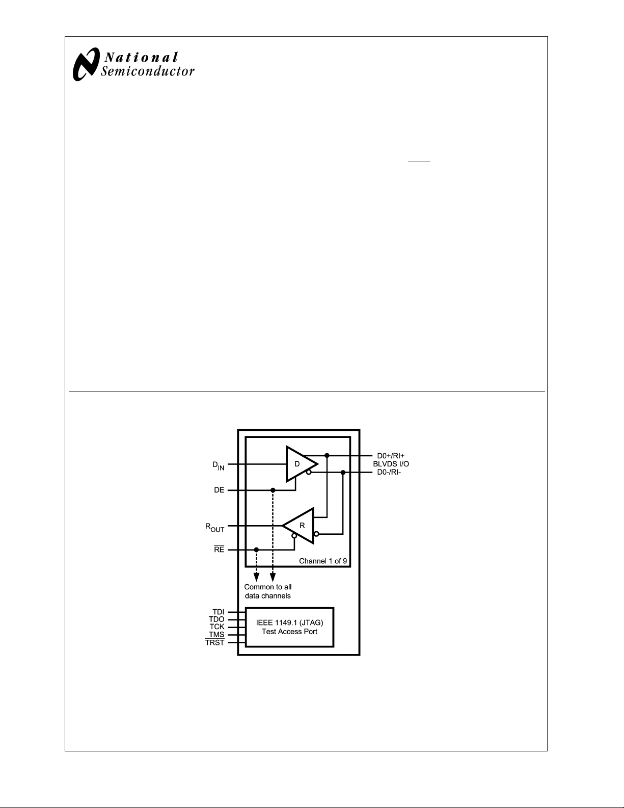
SCAN92LV090 9 Channel Bus LVDS Transceiver w/ Boundary SCAN
Simplified Functional Diagram
10124201
TRI-STATE®is a registered trademark of National Semiconductor Corporation.
© 2005 National Semiconductor Corporation DS101242 www.national.com
Page 2
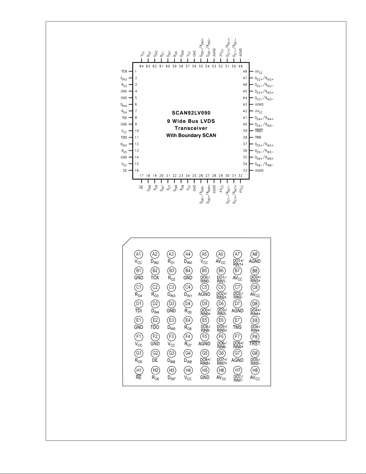
Connection Diagrams
SCAN92LV090
Top View
Order Number SCAN92LV090VEH
See NS Package Number VEH064DB
10124202
Top View
Order Number SCAN92LV090SLC
See NS Package Number SLC64A
www.national.com 2
10124216
Page 3
Pinout Description
Pin Name TQFP Pin # BGA Pin # Input/Output Descriptions
DO+/RI+ 27, 31, 35, 37, 41,
45, 47, 51, 55
DO−/RI− 26, 30, 34, 36, 40,
44, 46, 50, 54
D
IN
2, 6, 12, 18, 20, 22,
58, 60, 62
RO 3, 7, 13, 19, 21, 23,
59, 61, 63
RE
17 H1 I Receiver Enable TTL Input (Active Low).
DE 16 G2 I Driver Enable TTL Input (Active High).
GND 4, 5, 9, 14, 25, 56 B1, B4, D3, E1, F2,
V
CC
10, 15, 24, 57, 64 A1, A5, F1, F3, H4 Power VCCfor digital circuitry (must connect to VCCon PC
AGND 28, 33, 43, 49, 53 A8, C5, D7, F5, G7 Power Ground for analog circuitry (must connect to GND
AV
CC
TRST
29, 32, 42, 48, 52 A6, B7, C8, H6, H8 Power Analog VCC(must connect to VCCon PC board).
39 F8 I Test Reset Input to support IEEE 1149.1 (Active
TMS 38 E7 I Test Mode Select Input to support IEEE 1149.1
TCK 1 B2 I Test Clock Input to support IEEE 1149.1
TDI 8 D1 I Test Data Input to support IEEE 1149.1
TDO 11 E2 O Test Data Output to support IEEE 1149.1
A7, B8, C6, D5, D8,
E6, F7, G5, G6
B5, B6, C7, D6, E5,
E8, F6, G8, H7
A2, A4, C3, C4, D2,
E3, G3, G4, H3
A3, B3, C1, C2, D4,
E4, F4, G1, H2
H5
I/O True Bus LVDS Driver Outputs and Receiver Inputs.
I/O Complimentary Bus LVDS Driver Outputs and
Receiver Inputs.
I TTL Driver Input.
O TTL Receiver Output.
Power Ground for digital circuitry (must connect to GND on
PC board). These pins connected internally.
board). These pins connected internally.
on PC board). These pins connected internally.
These pins connected internally.
Low)
SCAN92LV090
www.national.com3
Page 4
Absolute Maximum Ratings
(Notes 2, 1)
If Military/Aerospace specified devices are required,
please contact the National Semiconductor Sales Office/
SCAN92LV090
Distributors for availability and specifications.
Supply Voltage (V
) 4.0V
CC
θ
ja
θ
jc
Junction Temperature +150˚C
Storage Temperature Range −65˚C to +150˚C
Lead Temperature
(Soldering, 4 sec.) 260˚C
Enable Input Voltage
(DE, RE)
Driver Input Voltage (D
) −0.3V to (VCC+0.3V)
IN
−0.3V to (VCC+0.3V)
Recommended Operating Conditions
Receiver Output Voltage
(R
) −0.3V to (VCC+0.3V)
OUT
Bus Pin Voltage (DO/RI
ESD (HBM 1.5 kΩ, 100 pF)
±
) −0.3V to +3.9V
>
4.5 kV
Driver Short Circuit Duration momentary
Receiver Short Circuit
Duration momentary
Maximum Package Power Dissipation at 25˚C
LQFP 1.74 W
Supply Voltage (V
) 3.0 3.6 V
CC
Receiver Input Voltage 0.0 2.4 V
Operating Free Air Temperature −40 +85 ˚C
Maximum Input Edge Rate
(Note 6)(20% to 80%) ∆t/∆V
Data 1.0 ns/V
Control 3.0 ns/V
Min Max Units
Derate LQFP Package 13.9 mW/˚C
DC Electrical Characteristics
Over recommended operating supply voltage and temperature ranges unless otherwise specified (Notes 2, 3)
Symbol Parameter Conditions Pin Min Typ Max Units
V
∆V
V
∆V
V
V
I
OSD
V
V
I
OD
V
V
V
I
IN
OD
OD
OS
OS
OH
OL
OH
OL
TH
TL
CMR
Output Differential
Voltage
RL=27Ω, Figure 1 DO+/RI+,
DO−/RI−
240 300 460 mV
VODMagnitude Change 27 mV
Offset Voltage 1.1 1.3 1.5 V
Offset Magnitude
Change
Driver Output High
Voltage
Driver Output Low
Voltage
Output Short Circuit
Current (Note 10)
Voltage Output High
(Note 11)
RL=27Ω
RL=27Ω
VOD= 0V, DE = VCC, Driver outputs
shorted together
VID= +300 mV IOH= −400 µA R
OUT
Inputs Open V
Inputs Terminated,
=27Ω
R
L
0.95 1.1 V
VCC−0.2 V
−0.2 V
CC
V
−0.2 V
CC
510mV
1.4 1.65 V
|36| |65| mA
Voltage Output Low IOL= 2.0 mA, VID= −300 mV 0.05 0.075 V
Receiver Output
Dynamic Current (Note
10)
Input Threshold High DE = 0V, VCM= 1.5V DO+/RI+,
Input Threshold Low −100 mV
Receiver Common Mode
Range
Input Current DE = 0V, RE = 2.4V,
= 300mV, V
V
ID
= −300mV, V
V
ID
OUT=VCC
OUT
−1.0V −110 |75|
= 1.0V |75|
DO−/RI−
VIN= +2.4V or 0V
V
= 0V, VIN= +2.4V or 0V −20
CC
110 mA
+100 mV
|VID|/2 2.4 −
|V
ID
−25
±
1 +25 µA
±
1 +20 µA
71.7˚C/W
10.9˚C/W
|/2
mA
V
www.national.com 4
Page 5

DC Electrical Characteristics (Continued)
Over recommended operating supply voltage and temperature ranges unless otherwise specified (Notes 2, 3)
Symbol Parameter Conditions Pin Min Typ Max Units
V
IH
V
IL
I
IH
I
IL
V
CL
I
IH
I
ILR
I
IL
I
CCD
I
CCR
I
CCZ
I
CC
I
CCS
I
OFF
C
OUTPUT
C
OUTPUT
Minimum Input High
Voltage
Maximum Input Low
Voltage
Input High Current VIN=VCCor 2.4V DIN, DE,
Input Low Current VIN= GND or 0.4V −20
Input Diode Clamp
I
CLAMP
= −18 mA
Voltage
Input High Current VIN=V
CC
DIN, DE,
RE, TCK,
TRST,
TMS, TDI
RE
TDI, TMS,
2.0 V
CC
GND 0.8 V
−20
±
10 +20 µA
±
10 +20 µA
−1.5 −0.8 V
-20 +20 µA
TCK,
TRST
Input Low Current VIN= GND, VCC= 3.6v TDI, TMS,
-25 -115 µA
TRST
Input Low Current VIN = GND TCK -20 +20 µA
Power Supply Current
Drivers Enabled,
No Load, DE = RE = V
DIN=VCCor GND
,
CC
V
CC
50 80 mA
Receivers Disabled
Power Supply Current
Drivers Disabled,
DE=RE=0V,V
=±300mV
ID
50 80 mA
Receivers Enabled
Power Supply Current,
Drivers and Receivers
TRI-STATE
®
Power Supply Current,
Drivers and Receivers
Enabled
Power Supply Current
(SCAN Test Mode),
Drivers and Receivers
Enabled
Power Off Leakage
Current
Capacitance@Bus Pins DO+/RI+,
Capacitance@R
OUT
DE = 0V; RE = VCC,
DIN=VCCor GND 50 80 mA
DE=V
DIN=VCCor GND,
R
L
DE=V
DIN=VCCor GND,
R
L
;RE=0V,
CC
=27Ω
;RE=0V,
CC
=27Ω, TAP in any state other
160 210 mA
180 230 mA
than Test-Logic-Reset
VCC= 0V or OPEN,
, DE, RE = 0V or OPEN,
D
IN
V
APPLIED
= 3.6V (Port Pins)
DO+/RI+,
DO−/RI− −20 +20 µA
DO−/RI−
R
OUT
5pF
7pF
V
SCAN92LV090
AC Electrical Characteristics
Over recommended operating supply voltage and temperature ranges unless otherwise specified (Note 6)
Symbol Parameter Conditions Min Typ Max Units
DIFFERENTIAL DRIVER TIMING REQUIREMENTS
t
PHLD
t
PLHD
t
SKD1
t
SKD2
t
SKD3
t
TLH
t
THL
Differential Prop. Delay High to Low (Note 8) RL=27Ω,
Differential Prop. Delay Low to High (Note 8) 1.0 1.8 2.6 ns
Differential Skew |t
PHLD–tPLHD
| (Note 9) 120 ps
Figure 2, Figure 3
=10pF
C
L
1.0 1.8 2.6 ns
Chip to Chip Skew (Note 12) 1.6 ns
Channel to Channel Skew (Note 13) 0.25 0.55 ns
Transition Time Low to High 0.5 1.2 ns
Transition Time High to Low 0.5 1.2 ns
www.national.com5
Page 6

AC Electrical Characteristics (Continued)
Over recommended operating supply voltage and temperature ranges unless otherwise specified (Note 6)
Symbol Parameter Conditions Min Typ Max Units
t
PHZ
SCAN92LV090
t
PLZ
t
PZH
t
PZL
DIFFERENTIAL RECEIVER TIMING REQUIREMENTS
t
PHLD
t
PLHD
t
SDK1
t
SDK2
t
SDK3
t
TLH
t
THL
t
PHZ
t
PLZ
t
PZH
t
PZL
SCAN CIRCUITRY TIMING REQUIREMENTS
f
MAX
t
S
t
H
t
S
t
H
t
W
t
W
t
REC
Note 1: “Absolute Maximum Ratings” are those values beyond which the safety of the device cannot be guaranteed. They are not meant to imply that the devices
should be operated at these limits. The table of “Electrical Characteristics” provides conditions for actual device operation.
Note 2: All currents into device pins are positive; all currents out of device pins are negative.All voltages are referenced to ground unless otherwise specified except
V
OD
Note 3: All typicals are given for V
Note 4: ESD Rating: HBM (1.5 kΩ, 100 pF)
Note 5: C
Note 6: Generator waveforms for all tests unless otherwise specified:f=25MHz, Z
minimum skew, data input edge rates should be equal to or faster than 1ns/V; control signals equal to or faster than 3ns/V. In general, the faster the input edge rate,
the better the AC performance.
Note 7: The DS92LV090A functions within datasheet specification when a resistive load is applied to the driver outputs.
Note 8: Propagation delays are guaranteed by design and characterization.
Note 9: t
Note 10: Only one output at a time should be shorted, do not exceed maximum package power dissipation capacity.
Note 11: V
Note 12: Chip to Chip skew is the difference in differential propagation delay between any channels of any devices, either edge.
Note 13: Channel to Channel skew is the difference in driver output or receiver output propagation delay between any channels within a device, common edge.
Disable Time High to Z RL=27Ω,
Disable Time Low to Z 38ns
Enable Time Z to High 38ns
Figure 4, Figure 5
=10pF
C
L
38ns
Enable Time Z to Low 38ns
Differential Prop. Delay High to Low (Note 8) Figure 6, Figure 7
=35pF
Differential Prop Delay Low to High (Note 8) 2.0 2.4 3.9 ns
Differential Skew |t
PHLD–tPLHD
| (Note 9) 210 ps
C
L
2.0 2.4 3.9 ns
Chip to Chip Skew (Note 12) 1.9 ns
Channel to Channel skew (Note 13) 0.35 0.7 ns
Transition Time Low to High 1.5 2.5 ns
Transition Time High to Low 1.5 2.5 ns
Disable Time High to Z RL= 500Ω,
Disable Time Low to Z 3.5 8 ns
Enable Time Z to High 3.5 8 ns
Figure 8, Figure 9
=35pF
C
L
4.5 10 ns
Enable Time Z to Low 3.5 8 ns
Maximum TCK Clock Frequency RL= 500Ω,CL=35pF25.0 75.0 MHz
TDI to TCK, H or L 1.5 ns
TDI to TCK, H or L 1.5 ns
TMS to TCK, H or L 2.5 ns
TMS to TCK, H or L 1.5 ns
TCK Pulse Width, H or L 10.0 ns
TRST Pulse Width, L 2.5 ns
Recovery Time, TRST to TCK 2.0 ns
, ∆VODand VID.
= +3.3V and TA= +25˚C, unless otherwise stated.
CC
includes probe and fixture capacitance.
L
SKD1|tPHLD–tPLHD
failsafe terminated test performed with 27Ω connected between RI+ and RI− inputs. No external voltage is applied.
OH
| is the worse case skew between any channel and any device over recommended operation conditions.
>
4.5 kV EIAJ (0Ω, 200 pF)>300V.
=50Ω,tr,tf=<1.0 ns (0%–100%). To ensure fastest propagation delay and
O
www.national.com 6
Page 7

SCAN92LV090
Applications Information
General application guidelines and hints may be found in the
following application notes: AN-808, AN-1108, AN-977,
AN-971, and AN-903.
There are a few common practices which should be implied
when designing PCB for Bus LVDS signaling. Recommended practices are:
Use at least 4 PCB board layer (Bus LVDS signals,
•
ground, power and TTL signals).
Keep drivers and receivers as close to the (Bus LVDS
•
port side) connector as possible.
Bypass each Bus LVDS device and also use distributed
•
bulk capacitance between power planes. Surface mount
capacitors placed close to power and ground pins work
best. Two or three high frequency, multi-layer ceramic
(MLC) surface mount (0.1 µF, 0.01 µF, 0.001 µF) in
parallel should be used between each V
The capacitors should be as close as possible to the V
pin.
Multiple vias should be used to connect V
planes to the pads of the by-pass capacitors.
In addition, randomly distributed by-pass capacitors
should be used.
Use the termination resistor which best matches the dif-
•
ferential impedance of your transmission line.
Leave unused Bus LVDS receiver inputs open (floating).
•
Limit traces on unused inputs to
Isolate TTL signals from Bus LVDS signals
•
<
0.5 inches.
MEDIA (CONNECTOR or BACKPLANE) SELECTION:
Use controlled impedance media. The backplane and
•
connectors should have a matched differential impedance.
and ground.
CC
and Ground
CC
CC
TABLE 1. Functional Table
MODE SELECTED DE RE
DRIVER MODE H H
RECEIVER MODE L L
TRI-STATE MODE L H
LOOP BACK MODE H L
TABLE 2. Transmitter Mode
INPUTS OUTPUTS
DE D
IN
DO+ DO−
HL LH
HH HL
<
H 0.8V
<
D
2.0V X X
IN
LXZZ
TABLE 3. Receiver Mode
INPUTS OUTPUT
RE
LL(
LH(
L −100 mV
(RI+) – (RI−)
<
−100 mV) L
>
+100 mV) H
<
V
ID
<
X
+100 mV
HX Z
X = High or Low logic state
L = Low state
Z = High impedance state
H = High state
Test Circuits and Timing Waveforms
FIGURE 1. Differential Driver DC Test Circuit
10124203
www.national.com7
Page 8

Test Circuits and Timing Waveforms (Continued)
SCAN92LV090
FIGURE 2. Differential Driver Propagation Delay and Transition Time Test Circuit
10124204
10124205
FIGURE 3. Differential Driver Propagation Delay and Transition Time Waveforms
10124206
FIGURE 4. Driver TRI-STATE Delay Test Circuit
www.national.com 8
Page 9

Test Circuits and Timing Waveforms (Continued)
FIGURE 5. Driver TRI-STATE Delay Waveforms
SCAN92LV090
10124207
10124208
FIGURE 6. Receiver Propagation Delay and Transition Time Test Circuit
FIGURE 7. Receiver Propagation Delay and Transition Time Waveforms
10124214
10124215
FIGURE 8. Receiver TRI-STATE Delay Test Circuit
www.national.com9
Page 10

Test Circuits and Timing Waveforms (Continued)
SCAN92LV090
FIGURE 9. Receiver TRI-STATE Delay Waveforms
Typical Bus Application Configurations
10124211
Bi-Directional Half-Duplex Point-to-Point Applications
Multi-Point Bus Applications
10124212
10124213
www.national.com 10
Page 11

SCAN92LV090
Description of Boundary-Scan Circuitry
The SCAN92LV090 features two unique Scan test modes,
each which requires a unique BSDL model depending on the
level of test access and fault coverage goals. In the first
mode (Mode0), only the TTL Inputs and Outputs of each
transceiver are accessible via a 1149.1 compliant protocol.
In the second mode (Mode1), the TTL Inputs and Outputs
are accessible by a 1149.1 compliant method while the
Differential I/O pins are accessible by a 1149.1 compatible
technique which evaluates the signal integrity and modifies
the data in the differential BSR as appropriate.
All test modes are handled by theATPG software, and BSDL
selection should be invisible to the user.
The BYPASS register is a single bit shift register stage
identical to scan cell TYPE1. It captures a fixed logic low.
Bypass Register Scan Chain Definition
Logic 0
10124209
The INSTRUCTION register is an eight-bit register which
captures the value 00111101.
Instruction Register Scan Chain Definition
10124210
MSB→LSB (Mode0)
Instruction Code Instruction
00000000 EXTEST
10000010 SAMPLE/PRELOAD
10000111 CLAMP
00000110 HIGHZ
All Others BYPASS
MSB→LSB (Mode1)
Instruction Code Instruction
10011001 EXTEST
10010010 SAMPLE/PRELOAD
10001111 CLAMP
00000110 HIGHZ
All Others BYPASS
Mode 0 Boundary Scan Register Configuration
10124220
Mode 1 Boundary Scan Register Configuration
10124221
www.national.com11
Page 12

Physical Dimensions inches (millimeters)
unless otherwise noted
SCAN92LV090
64-Lead Molded LQFP Package
Order Number SCAN92LV090VEH
NS Package Number VEH064DB
64-Lead Ball Grid Array Package
Order Number SCAN92LV090SLC
NS Package Number SLC64A
www.national.com 12
Page 13

Notes
SCAN92LV090 9 Channel Bus LVDS Transceiver w/ Boundary SCAN
National does not assume any responsibility for use of any circuitry described, no circuit patent licenses are implied and National reserves
the right at any time without notice to change said circuitry and specifications.
For the most current product information visit us at www.national.com.
LIFE SUPPORT POLICY
NATIONAL’S PRODUCTS ARE NOT AUTHORIZED FOR USE AS CRITICAL COMPONENTS IN LIFE SUPPORT DEVICES OR SYSTEMS
WITHOUT THE EXPRESS WRITTEN APPROVAL OF THE PRESIDENT AND GENERAL COUNSEL OF NATIONAL SEMICONDUCTOR
CORPORATION. As used herein:
1. Life support devices or systems are devices or systems
which, (a) are intended for surgical implant into the body, or
(b) support or sustain life, and whose failure to perform when
properly used in accordance with instructions for use
2. A critical component is any component of a life support
device or system whose failure to perform can be reasonably
expected to cause the failure of the life support device or
system, or to affect its safety or effectiveness.
provided in the labeling, can be reasonably expected to result
in a significant injury to the user.
BANNED SUBSTANCE COMPLIANCE
National Semiconductor manufactures products and uses packing materials that meet the provisions of the Customer Products
Stewardship Specification (CSP-9-111C2) and the Banned Substances and Materials of Interest Specification (CSP-9-111S2) and contain
no ‘‘Banned Substances’’ as defined in CSP-9-111S2.
National Semiconductor
Americas Customer
Support Center
Email: new.feedback@nsc.com
Tel: 1-800-272-9959
www.national.com
National Semiconductor
Europe Customer Support Center
Fax: +49 (0) 180-530 85 86
Email: europe.support@nsc.com
Deutsch Tel: +49 (0) 69 9508 6208
English Tel: +44 (0) 870 24 0 2171
Français Tel: +33 (0) 1 41 91 8790
National Semiconductor
Asia Pacific Customer
Support Center
Email: ap.support@nsc.com
National Semiconductor
Japan Customer Support Center
Fax: 81-3-5639-7507
Email: jpn.feedback@nsc.com
Tel: 81-3-5639-7560
 Loading...