

Page 1
EMBEDDED AND NETWORK COMPUTING TECHNOLOGIES
USERS GUIDE
SBC35-A9260-B01
Calao Systems
334 rue des Vingt Toises
Le Magistère II
38950 Saint Martin Le Vinoux
France
Phone = +33 (0)4 76 56 38 05
Fax = +33 (0)4 76 56 38 06
E-mail = sales@calao-systems.com
= support@calao-systems.com
Datasheet USG-00001-B01 1/28
Page 2
TABLE OF CONTENTS
Section 1...............................................................................................................................................3
1.Overview.......................................................................................................................................3
1.1.Scope.....................................................................................................................................3
1.2.Synoptic................................................................................................................................3
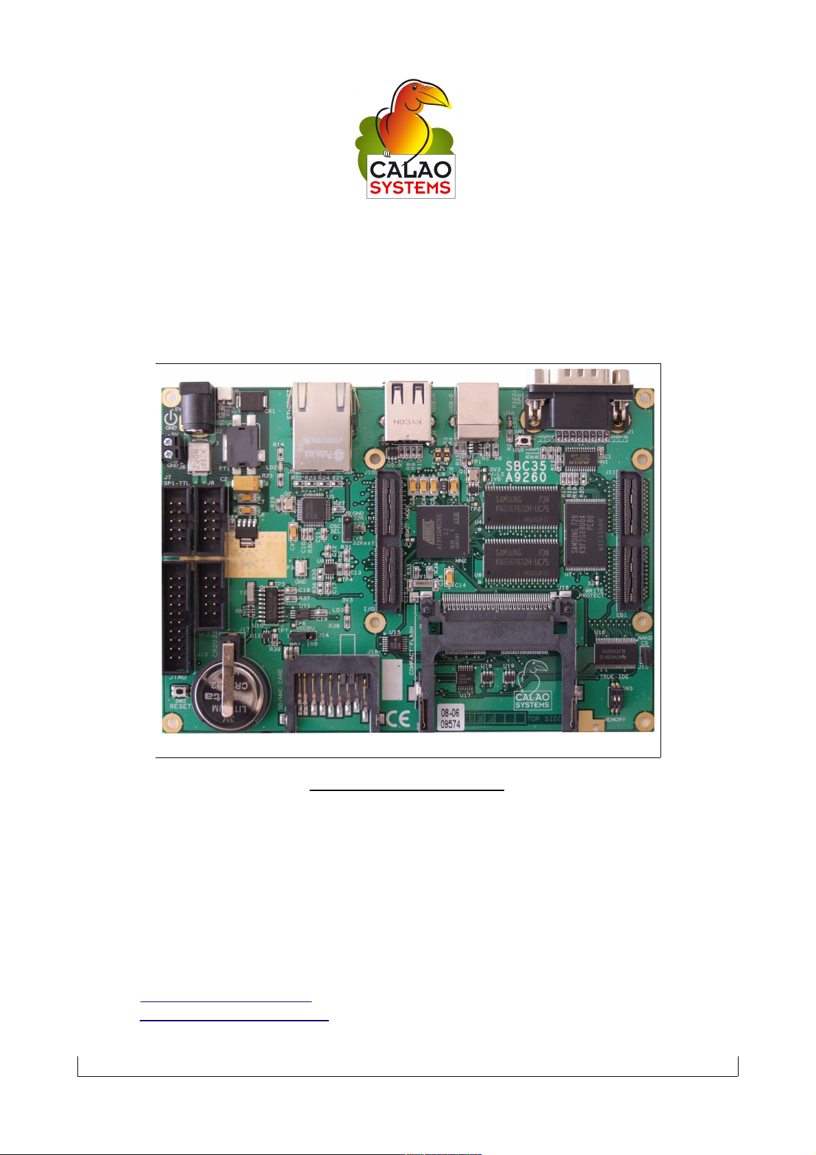
1.3.SBC35-A9260 Single Board Computer................................................................................4
Section 2 ..............................................................................................................................................5
1.Setting Up the SBC35-A9260 Board............................................................................................5
1.1.Electrostatic Warning............................................................................................................5
1.2.Requirements........................................................................................................................5
1.3.Layout...................................................................................................................................5
1.4.Powering Up the Board.........................................................................................................6
1.5.Getting Started......................................................................................................................6
Section 3...............................................................................................................................................7
1.Board Description.........................................................................................................................7
1.1.Microcontroller....................................................................................................................11
1.2.Memory...............................................................................................................................11
1.3.Clock Circuitry....................................................................................................................11
1.4.Reset Circuitry.....................................................................................................................11
1.5.Power Circuitry...................................................................................................................11
1.6.Remote Communication ....................................................................................................12
1.7.User Interface......................................................................................................................12
1.8.Debug Interface ..................................................................................................................12
1.9.Expansion slot.....................................................................................................................12
Section 4.............................................................................................................................................13
1.Configuration..............................................................................................................................13
1.1.Solder pads & switch configuration....................................................................................13
1.2.Memory...............................................................................................................................14
1.3.Ethernet...............................................................................................................................14
1.4.Miscellaneous......................................................................................................................14
1.5.Expansion connectors J10 & J11........................................................................................15
1.6.TTL serial port pinout J7, J8, J12........................................................................................18
Section 5.............................................................................................................................................19
1.Schematics..................................................................................................................................19
1.1.Schematics..........................................................................................................................19
Section 6.............................................................................................................................................28
1.Errata...........................................................................................................................................28
Section 7.............................................................................................................................................28
1.Revision History.........................................................................................................................28
1.1.Revision History.................................................................................................................28
Section 8.............................................................................................................................................28
1.COPYRIGHT..............................................................................................................................28
Datasheet USG-00001-B01 2/28
Page 3
SECTION 1
1. Overview
1.1. Scope
The
SBC35-A9260
SBC35-A9260 is a single board computer which runs a full linux environment. It allows
to develop applications on a host computer using cross-compilation toolchain and install the
results on the
SBC35-A9260
SBC35-A9260. This guide focuses on the SBC35-A9260 board as an
industrial board.
The board is equiped with an AT91SAM9260 processor in an LFBGA217 package.
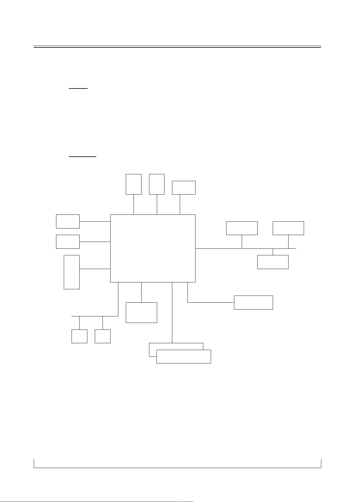
1.2. Synoptic
Datasheet USG-00001-B01 3/28
UHP
x2
UDP
AT91SAM9260
SDRAM
64Mb
Nand Flas h
256Mb
CF-Slot
Port
COM-0
JTAG
SD/MMC
Slot
Expans ion connector
x2
Ethernet
RTC E2P
Port
COM-1
Port
COM-2
Page 4

1.3. SBC35-A9260 Single Board Computer
The board is equipped with an AT91SAM9260 (217-ball LFBGA package) together with the
following:
● 64Mbytes of SDRAM memory
● 256Mbytes of NANDFlash memory
● 1x 64Kbytes SPI serial eeprom
● 1x M41T94 SPI real-time clock with 44bytes NVRAM
● 1x USB device port interface
● 2x USB Host port interfaces
● 1x RS232 serial port with full handshacking
● 2x serial ports TTL level signals
● 1x DBGU serial port TTL level signals
● 1x JTAG/ICE debug interface (20pins JTAG port)
● 1x 10/100baseTx port
● 1x power led and one general purpose LED
● 1x user push button
● 1x reset button
● 1x SD/MMC socket
● 1x Compact flash socket
● 2x Expansion connectors
Datasheet USG-00001-B01 4/28
Page 5
SECTION 2
1. Setting Up the SBC35-A9260 Board
1.1. Electrostatic Warning
The SBC35-A9260 board is shipped in protective anti-static packaging. The board must not
be subjected to high electrostatic potentials. A grounding strap or similar protective device
should be worn when handling the board. Avoid touching the component pins or any other
metallic element.
1.2. Requirements
In order to set up the SBC35-A9260 board, the following items are needed:
● the SBC35-A9260 board itself.
● AC/DC power adapter (5V at 2A), 2.1 mm by 5.5 mm
1.3. Layout
Datasheet USG-00001-B01 5/28
Page 6
1.4. Powering Up the Board
The SBC35-A9260 requires 5V DC (±5%). DC power is supplied to the board via J3.
Coaxial plug center positive standard.
1.5. Getting Started
The SBC35-A9260 board is delivered with a pre-installed U-Boot boot loader and an
Embedded Linux operating system. These two components are stored in the NAND Flash.
You can update your board by downloading all the available sources and tools on the calao website
www.calao-systems.com in order to adapt your system to your needs.
Datasheet USG-00001-B01 6/28
Page 7

SECTION 3
1. Board Description
AT91SAM9260 Microcontroller:
Incorporates the ARM926EJ-S™ ARM® Thumb® Processor
✔ DSP Instruction Extensions, ARM Jazelle® Technology for Java®Acceleration
✔ 8-KByte Data Cache, 8-KByte Instruction Cache, Write Buffer
✔ 200 MIPS at 180 Mhz
✔ Memory Management Unit
✔ EmbeddedICE™, Debug Communication Channel Support
Additional Embedded Memories
✔ One 32-KByte Internal ROM, Single-cycle Access At Maximum Matrix Speed
✔ Two 4-KByte Internal SRAM, Single-cycle Access At Maximum Matrix Speed
External Bus Interface (EBI)
✔ Supports SDRAM, Static Memory, ECC-enabled NANDFlash and CompactFlash®
USB 2.0 Full Speed (12 Mbits per second) Device Port
✔ On-chip Transceiver, 2,432-byte Configurable Integrated DPRAM
USB 2.0 Full Speed (12 Mbits per second) Host Single Port in the 208-lead PQFP Package
and Double Port in 217-ball LFBGA Package
✔ Single or Dual On-chip Transceivers
✔ Integrated FIFOs and Dedicated DMA Channels
Ethernet MAC 10/100 Base T
✔ Media Independant Interface or Reduced Media Independant Interface
✔ 28-byte FIFOs and Dedicated DMA Channels for Receive and Transmit
Image Sensor Interface
✔ ITU-R BT. 601/656 External Interface, Programmable Frame Capture Rate
✔ 12-bit Data Interface for Support of High Sensibility Sensors
✔ SAV and EAV Synchronization, Preview Path with Scaler, YCbCr Format
■ Bus Matrix
✔ Six 32-bit-layer Matrix
✔ Boot Mode Select Option, Remap Command
Fully-featured System Controller, including
✔ Reset Controller, Shutdown Controller
✔ Four 32-bit Battery Backup Registers for a Total of 16 Bytes
✔ Clock Generator and Power Management Controller
✔ Advanced Interrupt Controller and Debug Unit
✔ Periodic Interval Timer, Watchdog Timer and Real-time Timer
Datasheet USG-00001-B01 7/28
Page 8

Reset Controller (RSTC)
✔ Based on a Power-on Reset Cell, Reset Source Identification and Reset Output Control
Clock Generator (CKGR)
✔ Selectable 32768Hz Low-power Oscillator or Internal Low Power RC Oscillator on
Battery Backup Power Supply, Providing a Permanent Slow Clock
✔ 3 to 20 MHz On-chip Oscillator, One up to 240 MHz PLL and One up to 130 MHz PLL
Power Management Controller (PMC)
✔ Very Slow Clock Operating Mode, Software Programmable Power Optimization
Capabilities
✔ Two Programmable External Clock Signals
Advanced Interrupt Controller (AIC)
✔ Individually Maskable, Eight-level Priority, Vectored Interrupt Sources
✔ Three External Interrupt Sources and One Fast Interrupt Source, Spurious Interrupt
Protected
Debug Unit (DBGU)
✔ 2-wire UART and Support for Debug Communication Channel, Programmable ICE
Access Prevention
Periodic Interval Timer (PIT)
✔ 20-bit Interval Timer plus 12-bit Interval Counter
Watchdog Timer (WDT)
✔ Key-protected, Programmable Only Once, Windowed 16-bit Counter Running at Slow
Clock
Real-time Timer (RTT)
✔ 32-bit Free-running Backup Counter Running at Slow Clock with 16-bit Prescaler
✔ One 4-channel 10-bit Analog-to-Digital Converter
✔ Three 32-bit Parallel Input/Output Controllers (PIOA, PIOB, PIOC)
✔ 96 Programmable I/O Lines Multiplexed with up to Two Peripheral I/Os
✔ Input Change Interrupt Capability on Each I/O Line
✔ Individually Programmable Open-drain, Pull-up Resistor and Synchronous Output
✔ High-current Drive I/O Lines, Up to 16 mA Each
Peripheral DMA Controller Channels (PDC)
One Two-slot MultiMedia Card Interface (MCI)
✔ SDCard/SDIO and MultiMediaCard™ Compliant
✔ Automatic Protocol Control and Fast Automatic Data Transfers with PDC
One Synchronous Serial Controller (SSC)
✔ Independent Clock and Frame Sync Signals for Each Receiver and Transmitter
✔ I²S Analog Interface Support, Time Division Multiplex Support
✔ High-speed Continuous Data Stream Capabilities with 32-bit Data Transfer
Datasheet USG-00001-B01 8/28
Page 9

Four Universal Synchronous/Asynchronous Receiver Transmitters (USART)
✔ Individual Baud Rate Generator, IrDA® Infrared Modulation/Demodulation,
Manchester Encoding/Decoding
✔ Support for ISO7816 T0/T1 Smart Card, Hardware Handshaking, RS485 Support
✔ Full Modem Signal Control on USART0
Two 2-wire UARTs
Two Master/Slave Serial Peripheral Interfaces (SPI)
✔ 8- to 16-bit Programmable Data Length, Four External Peripheral Chip Selects
✔ Synchronous Communications
Two Three-channel 16-bit Timer/Counters (TC)
✔ Three External Clock Inputs, Two Multi-purpose I/O Pins per Channel
✔ Double PWM Generation, Capture/Waveform Mode, Up/Down Capability
✔ High-Drive Capability on Ouputs TIOA0, TIOA1, TIOA2
One Two-wire Interface (TWI)
✔ Master, Multi-master and Slave Mode Operation
✔ General Call Supported in Slave Mode
✔ Connection to PDC Channel To Optimize Data Transfers in Master Mode Only
IEEE® 1149.1 JTAG Boundary Scan on All Digital Pins
Required Power Supplies:
✔ 1.65V to 1.95V for VDDBU, VDDCORE, VDDOSC and VDDPLL
✔ 3.0V to 3.6V for VDDIOP0, VDDIOP1 (Peripheral I/Os) and VDDANA (Analog to
Digital Converter)
✔ Programmable 1.65V to 1.95V or 3.0V to 3.6V for VDDIOM (Memory I/Os)
Available in a 208-lead PQFP and 217-ball LFBGA Package
Datasheet USG-00001-B01 9/28
Page 10

AT91SAM9260 Block Diagram
Datasheet USG-00001-B01 10/28
Page 11

1.1. Microcontroller
1x LFBGA 217-ball fitted on board
1.2. Memory
1x 32Kbytes of internal ROM
2x 4Kbytes of internal SRAM
1x 64Kbytes SPI EEPROM memory
1x 64Mbytes of SDRAM memory (32 bits bus width)
1x 256Mbytes of NAND Flash memory (8bits bus width)
Bank Start address Size Description
Internal memories 0x00000000 256Mbytes
EBI CS0 0x10000000 256Mbytes Expansion connectors
EBI CS1 (SDRAMC) 0x20000000 64Mbytes Soldered SDRAM
EBI CS2 0x30000000 Not available
EBI CS3 (NAND) 0x40000000 256Mbytes Soldered NAND Flash
EBI CS4 (CF slot 0) 0x50000000 - Compact Flash Interface
EBI CS5 0x60000000 256Mbytes Expansion connectors
EBI CS6 0x70000000 Not available
EBI CS7 0x80000000 256Mbytes Expansion connectors
1.3. Clock Circuitry
12Mhz standard oscillator
Selectable 32768Hz low power external standard crystal Oscillator or internal low power
RC oscillator
1.4. Reset Circuitry
Internal reset controller with bi-directional reset pin
External reset pushbutton
1.5. Power Circuitry
On board 1.8V low dropout linear regulator
On board 3.3V low dropout linear regulator
Datasheet USG-00001-B01 11/28
Page 12

1.6. Remote Communication
1x complete modem serial interface (COM Port 0) via RS232 DB9 male connector
2x additional serial interfaces with RTS/CTS handshake control via HE10-2x5 connector
(TTL level signals)
1x DBGU serial port TTL via HE10-2x5 (TTL level signals)
2x USB Host ports V2.0 full speed compliant, 12Mbits per second (UHP)
1x USB V2.0 full speed compliant, 12Mbits per second (UDP)
1x Ethernet 100-base TX with three status LED
1.7. User Interface
1x user orange led (LD1)
1x user input pushbutton (SW1)
1.8. Debug Interface
20-pin HE10-2x5 JTAG/ICE interface connector
HE10-2x5 DBGU COM Port
1.9. Expansion slot
1x SD/MMC card slot
1x Compact Flash card slot
2x Expansion connectors.
These two expansion connectors allow the developer to extend the features of the board by
adding external hardware components or boards.
Datasheet USG-00001-B01 12/28
Page 13

SECTION 4
1. Configuration
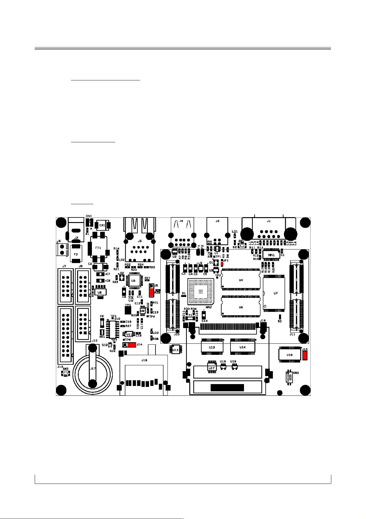
1.1. Solder pads & switch configuration
Designation Default setting Feature
JP1 2-3 Xin OSC Input level voltage
1-2 : 3.3V
2-3: 1.8V
J9 2-3 Slow Clock OSCSEL
1-2: internal RC osc.
2-3: Ext crystal osc.
J14 1-2 VDDBU
1-2: Lithium 3V Battery
2-3: 1.8V from VDDCORE
J15 1-2 NAND chipselect
opened: nand chipselect not connected
closed: nand chipselect connected
SW3 on CF mode selection
on: CF interface in true ide mode
off: CF interface in memory/io mode
S1 opened Boot configuration
opened: boot from internal ROM
closed: boot from NCS0
Datasheet USG-00001-B01 13/28
Page 14

S2
opened Nand write protect:
opened: write protection disabled
closed: write protection enabled
1.2. Memory
Memory configuration
Designation Default setting Feature
SDRAM U4 & U8
R60
R65
Soldered
Soldered
Enables U4 (D[16..31])chip select access
Enables U8 (D[0..15]) chip select access
NANDFlash U7
J15
R71
S2
closed
Soldered
Opened
Enables the use of NANDFlash
Enables the use of Ready/busy signal
Disables write protect
1.3. Miscellaneous
Designation Default setting Feature
R15 soldered USB device: Enables the use of USBCNX signal.
R46
R47
R45
R19
R18
R52
R16
R17
R53
soldered
soldered
soldered
soldered
soldered
soldered
soldered
soldered
soldered
RTS0
TXD0
DTR0
DCD0
DSR0
RXD0
CTS0
RI0
Receiver outputs enabled.
Datasheet USG-00001-B01 14/28
Page 15

1.4. Ethernet
The Ethernet PHY DP83848 is wired in RMII mode.
1.5. Expansion connectors J10 & J11
● EBI expansion connector (J11)
Pin Description Pin Description
1 D31 2 D30
3 A9 4 A6
5 D29 6 D28
7 A8 8 A7
9 D27 10 D26
11 A11 12 A10
13 D25 14 D24
15 A13 16 A14
17 D23 18 D22
19 D11 20 D10
21 D21 22 D20
23 CFIOW_NBS3_NWR3 24 A1
25 D19 26 D18
27 D13 28 D15
29 D17 30 D16
31 D14 32 D12
33 GND 34 GND
35 CFIOR_NBS1_NWR1 36 D9
37 GND 38 GND
39 D8 40 A2
41 GND 42 GND
43 A3 44 A4
45 GND 46 GND
47 A5 48 A16
49 GND 50 GND
51 A17 52 PC4/A23
53 GND 54 GND
55 D7 56 D6
Datasheet USG-00001-B01 15/28
Page 16

57 GND 58 GND
59 D5 60 D4
61 GND 62 GND
63 D3 64 D2
65 GND 66 GND
67 D1 68 D0
69 GND 70 GND
71 A12 72 A15
73 GND 74 GND
75 A20 76 A18
77 GND 78 GND
79 A19 80 A21
81 GND 82 GND
83 PC9/NCS5/CFCS1 84 A22
85 GND 86 GND
87 PC12/IRQ0/NCS7 88 CFWE_NWE_NWR0
89 +3.3V 90 +3.3V
91 CFOE_NRD 92 NCS0
93 +3.3V 94 +3.3V
95 NRST 96 PC15/NWAIT/IRQ1
97 +3.3V 98 +3.3V
99 A0 100 NC
Datasheet USG-00001-B01 16/28
Page 17

● GPIO expansion connector (J10)
Pin Description Pin Description
1 GND 2 GND
3 +3.3V 4 +3.3V
5 GND 6 GND
7 +3.3V 8 +3.3V
9 GND 10 GND
11 PB0/SPI1_MISO/TIOA3 12 PA23/TWD
13 GND 14 GND
15 PB1/SPI1_MOSI/TIOB3 16 PA24/TWCK
17 GND 18 GND
19 PB2/SPI1_SPCK/TIOA4 20 PA25/TCLK0
21 GND 22 GND
23 PB3/SPI1_NPCS0/TIOA5 24 PA26/TIOA0
25 GND 26 GND
27 PB16/TK0/TCLK3 28 PA27/TIOA1
29 GND 30 GND
31 PB17/TF0/TCLK4 32 PA28/TIOA2
33 GND 34 GND
35 PB18/TD0/TIOB4 36 PA29/SCK1
37 GND 38 GND
39 PB19/RD0/TIOB5 40 PA22/ADTRG
41 GND 42 GND
43 PB20/RK0 44 NC
45 GND 46 GND
47 PB30/PCK0 48 NC
49 GND 50 GND
51 GND 52 GND
53 +3.3V 54 +3.3V
55 GND 56 GND
57 +3.3V 58 +3.3V
59 GND 60 GND
61 PC0/SCK3/AD0 62 NC
63 GND 64 GND
65 PC1/PCK0/AD1 66 NC
Datasheet USG-00001-B01 17/28
Page 18

67 GND 68 GND
69 PC2/PCK1/AD2 70 NC
71 GND 72 GND
73 NC 74 NC
75 GND 76 GND
77 WKUP 78 NC
79 GND 80 GND
81 SHDN 82 NC
83 GND 84 GND
85 PB11 86 NC
87 GND 88 GND
89 PB31/PCK1 90 NC
91 GND 92 GND
93 NC 94 NC
95 GND 96 GND
97 NC 98 NC
99 GND 100 GND
1.6. TTL serial port pinout J7, J8, J12
● Debug Port: J12
Pin Description Pin Description
1 NC 2 NC
3 DRXD 4 NC
5 DTXD 6 NC
7 NC 8 NC
9 GND 10 +3.3V
● COM1 Port: J7
Pin Description Pin Description
1 NC 2 NC
3 RXD1 4 RTS1
5 TXD1 6 CTS1
7 NC 8 NC
9 GND 10 +3.3V
Datasheet USG-00001-B01 18/28
Page 19

● COM2 Port: J8
Pin Description Pin Description
1 NC 2 NC
3 RXD2 4 RTS2
5 TXD2 6 CTS2
7 NC 8 NC
9 GND 10 +3V3
Datasheet USG-00001-B01 19/28
Page 20

SECTION 5
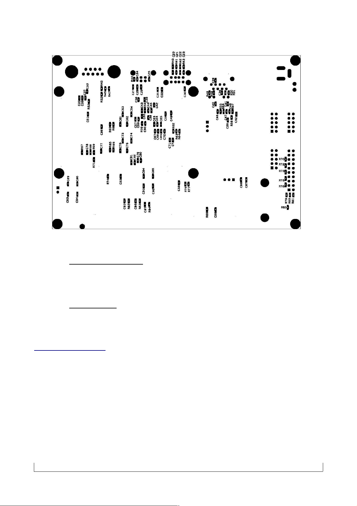
1. Schematics
1.1. Schematics
Datasheet USG-00001-B01 20/28
Page 21

Datasheet USG-00001-B01 21/28
Page 22

Datasheet USG-00001-B01 22/28
Page 23

Datasheet USG-00001-B01 23/28
Page 24

Datasheet USG-00001-B01 24/28
Page 25

Datasheet USG-00001-B01 25/28
Page 26

Datasheet USG-00001-B01 26/28
Page 27

Datasheet USG-00001-B01 27/28
Page 28

SECTION 6
1. Errata
SECTION 7
1. Revision History
1.1. Revision History
Date Version Remarks
2008-10-10 B01 first version
SECTION 8
1. COPYRIGHT
Notice: The products specifications provided in this datasheet are subject to change
without notice.
©2007 CALAO SYSTEMS-All Rights Reserved.
The CALAO SYSTEMS logo is a registered trademark of CALAO SYSTEMS.
All other names are the property of their respective owners.
Datasheet USG-00001-B01 28/28
 Loading...