

Page 1

G
M
6
S
a
3
s
a
_
w
_
r
D
s
c
B
LTE
Rev.
Date:
Statu
odule
BG96_H
2019-0
s: Relea
9
H
eries
rdware
-13
ed
rd
Design
a
V1.4
e
e
ig
n
www.que
tel.com
Page 2
LTE Module Series
BG96 Hardware Design
Our aim is to provide customers with timely and comprehensive service. For any
assistance, please contact our company headquarters:
Quectel Wireless Solutions Co., Ltd.
7th Floor, Hongye Building, No.1801 Hongmei Road, Xuhui District, Shanghai 200233, China
Tel: +86 21 5108 6236
Email:info@quectel.com
Or our local office. For more information, please visit:
http://quectel.com/support/sales.htm
For technical support, or to report documentation errors, please visit:
http://quectel.com/support/technical.htm
Or email to: support@quectel.com
GENERAL NOTES
QUECTEL OFFERS THE INFORMATION AS A SERVICE TO ITS CUSTOMERS. THE INFORMATION
PROVIDED IS BASED UPON CUSTOMERS’ REQUIREMENTS. QUECTEL MAKES EVERY EFFORT
TO ENSURE THE QUALITY OF THE INFORMATION IT MAKES AVAILABLE. QUECTEL DOES NOT
MAKE ANY WARRANTY AS TO THE INFORMATION CONTAINED HEREIN, AND DOES NOT ACCEPT
ANY LIABILITY FOR ANY INJURY, LOSS OR DAMAGE OF ANY KIND INCURRED BY USE OF OR
RELIANCE UPON THE INFORMATION. ALL INFORMATION SUPPLIED HEREIN IS SUBJECT TO
CHANGE WITHOUT PRIOR NOTICE.
COPYRIGHT
THE INFORMATION CONTAINED HERE IS PROPRIETARY TECHNICAL INFORMATION OF
QUECTEL WIRELESS SOLUTIONS CO., LTD. TRANSMITTING, REPRODUCTION, DISSEMINATION
AND EDITING OF THIS DOCUMENT AS WELL AS UTILIZATION OF THE CONTENT ARE
FORBIDDEN WITHOUT PERMISSION. OFFENDERS WILL BE HELD LIABLE FOR PAYMENT OF
DAMAGES. ALL RIGHTS ARE RESERVED IN THE EVENT OF A PATENT GRANT OR
REGISTRATION OF A UTILITY MODEL OR DESIGN.
Copyright © Quectel Wireless Solutions Co., Ltd. 2019. All rights reserved.
BG96_Hardware_Design 1 / 81
Page 3
BG96 Hardware Design
About the Document
History
Revision Date Author Description
Lyndon LIU/
1.0 2017-08-04
Daryl DU
Initial
LTE Module Series
1.1 2017-08-31 Daryl DU
1.2 2017-12-22
Lyndon LIU/
Daryl DU
1. Modified GSM features in Table 2.
2. Added a note for e-I-DRX in Chapter 3.3.
3. Elaborated the description of e-I-DRX in Chapter 3.4.3.
4. Updated RF receiving sensitivity in Chapter 6.6.
1. Added the storage temperature of the module in Table
2 and Chapter 6.3.
2. Updated transmitting power values in Table 2.
3. Added the description of sleep mode in Table 5 and
Chapter 3.4.4.
4. Added the description of ADC interfaces in Chapter
3.16.
5. Updated the GNSS performance in Table 21.
6. Updated the peak supply current values in Table 28.
7. Updated the current consumption valuesin Chapter
6.4.
8. Updated RF output power values inTable 34.
9. Updated LTE Cat NB1 RF receiving sensitivityvalues
(without repetitions) in Table 35.
10. Updated the recommended footprintin Chapter 7.2.
Lyndon LIU/
Daryl DU/
1.3 2018-07-12
Hyman
DING
BG96_Hardware_Design 2 / 81
1. Updated the timing of turning on module in Figure 8.
2. Updated theUSB interfacereference design(Figure 15).
3. Added the description of GPIO interfaces (Chapter
3.17).
4. Updated GNSS performance parameters in Table 25.
5. Updated the GNSS antenna interface reference design
(Figure 27).
Page 4

BG96 Hardware Design
Lyndon LIU/
1.4 2019-03-13
Rex WANG
LTE Module Series
6. Updated GNSS current consumption parameters in
Table 35.
7. Updated the module’s baking temperatureand baking
hours in Chapter 8.1.
1. Updated the general description in Chapter 2.1.
2. Updated and added the BG96-M module in Table 1.
3. Updated the internal protocol features and USB
interface in Table 2.
4. Updated the functional diagram in Figure 1.
5. Opened the W_DISABLE# pin function in the related
Chapters.
6. Updated the DC characteristics of PWRKEY pin in
Table 4.
7. Updated the description and star structure of the
power supply figure in Chapter 3.5.2
8. Updated the timing of turning on module in Figure 8.
9. Updated the Characteristics of ADC interfaces in Table
22.
10. Updated BG96 module info and added BG96-M
module in Chapter 5.1.2.
11. Updated the GNSS frequency in Table 29.
12. Updated theantenna requirements in Table 30.
13. Updated the current consumption in Table 34.
14. Added B25 output power in Table 36.
15. Updated BG96 and added BG96-Mconducted RF
receiving sensitivity in Chapter 6.6.
16. Updated the reel packaging info in Table 40.
BG96_Hardware_Design 3 / 81
Page 5

LTE Module Series
BG96 Hardware Design
Contents
About the Document ................................................................................................................................ 2
Contents .................................................................................................................................................... 4
Table Index ............................................................................................................................................... 6
Figure Index .............................................................................................................................................. 8
1 Introduction ....................................................................................................................................... 9
1.1. Safety Information .................................................................................................................. 10
1.2. FCC/ISED Regulatory notices ................................................................................................ 12
2 Product Concept ............................................................................................................................. 14
2.1. General Description ................................................................................................................ 14
2.2. Key Features .......................................................................................................................... 15
2.3. Functional Diagram ................................................................................................................ 17
2.4. Evaluation Board .................................................................................................................... 18
3 Application Interfaces ..................................................................................................................... 20
3.1. Pin Assignment ....................................................................................................................... 21
3.2. Pin Description ....................................................................................................................... 23
3.3. Operating Modes .................................................................................................................... 30
3.4. Power Saving ......................................................................................................................... 31
3.4.1. Airplane Mode
.............................................................................................................. 31
3.4.2. Power Saving Mode(PSM)........................................................................................... 31
3.4.3. Extended Idle Mode DRX(e-I-DRX) ............................................................................. 32
3.4.4. Sleep Mode.................................................................................................................. 34
3.4.4.1. UART Application ............................................................................................... 34
3.5. Power Supply ......................................................................................................................... 35
3.5.1. Power Supply Pins ....................................................................................................... 35
3.5.2. Decrease Voltage Drop ................................................................................................ 35
3.5.3. Monitor the Power Supply ............................................................................................ 37
3.6. Turn on and off Scenarios ...................................................................................................... 37
3.6.1. Turn on Module Using the PWRKEY Pin ..................................................................... 37
3.6.2. Turn off Module ............................................................................................................ 39
3.6.2.1. Turn off Module Using the PWRKEY Pin ........................................................... 39
3.6.2.2. Turn off Module Using AT Command ................................................................. 40
3.7. Reset the Module ................................................................................................................... 40
3.8. (U)SIM Interface ..................................................................................................................... 42
3.9. USB Interface ......................................................................................................................... 45
3.10.
UART Interfaces ..................................................................................................................... 46
3.11. PCM* and I2C* Interfaces ...................................................................................................... 49
3.12. Network Status Indication ....................................................................................................... 50
3.13. STATUS .................................................................................................................................. 52
BG96_Hardware_Design 4 / 81
Page 6

LTE Module Series
BG96 Hardware Design
3.14. Behaviors of RI ....................................................................................................................... 52
3.15. USB_BOOT Interface ............................................................................................................. 53
3.16. ADC Interfaces ....................................................................................................................... 54
3.17. GPIOInterfaces ....................................................................................................................... 55
4 GNSS Receiver ................................................................................................................................ 57
4.1. General Description ................................................................................................................ 57
4.2. GNSS Performance ................................................................................................................ 57
4.3. Layout Guidelines ................................................................................................................... 58
5 Antenna Interfaces .......................................................................................................................... 59
5.1. MainAntenna Interface ........................................................................................................... 59
5.1.1. Pin Definition ................................................................................................................ 59
5.1.2. Operating Frequency ................................................................................................... 59
5.1.3. Reference Design of RF Antenna Interface ................................................................. 61
5.1.4. Reference Design of RF Layout ................................................................................... 61
5.2. GNSS Antenna Interface ........................................................................................................ 64
5.3. Antenna Installation ................................................................................................................ 65
5.3.1. Antenna Requirements ................................................................................................ 65
5.3.2. Recommended RF Connector for Antenna Installation ................................................ 66
6 Electrical, Reliability and RadioCharacteristics ........................................................................... 69
6.1. Absolute Maximum Ratings .................................................................................................... 69
6.2. Power Supply Ratings ............................................................................................................ 69
6.3. Operation and StorageTemperatures ..................................................................................... 70
6.4. Current Consumption ............................................................................................................. 71
6.5. RF Output Power .................................................................................................................... 75
6.6. RF Receiving Sensitivity ......................................................................................................... 76
6.7. Electrostatic Discharge ........................................................................................................... 78
7 Mechanical Dimensions.................................................................................................................. 79
7.1. Mechanical Dimensions of the Module ................................................................................... 79
7.2. Recommended Footprint ........................................................................................................ 81
7.3. Design Effect Drawings of the Module .................................................................................... 82
8 Storage, Manufacturing and Packaging ........................................................................................ 84
8.1. Storage ................................................................................................................................... 84
8.2.
Manufacturing and Soldering .................................................................................................. 85
8.3. Packaging ............................................................................................................................... 86
9 Appendix A References .................................................................................................................. 88
10 Appendix B GPRS Coding Schemes ............................................................................................. 91
11 Appendix C GPRS Multi-slot Classes ............................................................................................ 92
12 Appendix D EDGE Modulationand Coding Schemes ................................................................... 94
BG96_Hardware_Design 5 / 81
Page 7

LTE Module Series
BG96 Hardware Design
Table Index
TABLE 1: FREQUENCY BANDS OF BG96 MODULE ...................................................................................... 14
TABLE 2: KEY FEATURES OF BG96 MODULE ............................................................................................... 15
TABLE 3: DEFINITION OF I/O PARAMETERS ................................................................................................. 23
TABLE 4: PIN DESCRIPTION ........................................................................................................................... 23
TABLE 5: OVERVIEW OF OPERATING MODES ............................................................................................. 30
TABLE 6: VBAT AND GND PINS ....................................................................................................................... 35
TABLE 7: PIN DEFINITION OF PWRKEY ........................................................................................................ 37
TABLE 8: RESET_N PIN DESCRIPTION ......................................................................................................... 40
TABLE 9: PIN DEFINITION OF (U)SIM INTERFACE ....................................................................................... 42
TABLE 10: PIN DEFINITION OF USB INTERFACE ......................................................................................... 45
TABLE 11: PIN DEFINITION OF UART1 INTERFACE ..................................................................................... 47
TABLE 12: PIN DEFINITION OF UART2 INTERFACE ..................................................................................... 47
TABLE 13: PIN DEFINITION OF UART3 INTERFACE ..................................................................................... 47
TABLE 14:LOGIC LEVELS OF DIGITAL I/O ..................................................................................................... 48
TABLE 15: PIN DEFINITION OF PCM AND I2C INTERFACES ....................................................................... 49
TABLE 16: PIN DEFINITION OF NETLIGHT .................................................................................................... 51
TABLE 17: WORKING STATE OF NETLIGHT .................................................................................................. 51
TABLE 18: PIN DEFINITION OF STATUS ........................................................................................................ 52
TABLE 19: DEFAULT BEHAVIORS OF RI ........................................................................................................ 53
TABLE 20: PIN DEFINITION OF USB_BOOT INTERFACE ............................................................................. 54
TABLE 21: PIN DEFINITION OF ADC INTERFACES ....................................................................................... 55
TABLE 22: CHARACTERISTICS OF ADC INTERFACES ................................................................................ 55
TABLE 23: PIN DEFINITION OF GPIO INTERFACES ..................................................................................... 56
TABLE 24:LOGIC LEVELS OF GPIO INTERFACES ........................................................................................ 56
TABLE 25: GNSS PERFORMANCE ................................................................................................................. 57
TABLE 26: PIN DEFINITION OF MAIN ANTENNA INTERFACE ...................................................................... 59
TABLE 27: BG96 OPERATING FREQUENCY .................................................................................................. 59
TABLE 28: PIN DEFINITION OF GNSS ANTENNA INTERFACE ..................................................................... 64
TABLE 29: GNSS FREQUENCY ....................................................................................................................... 64
TABLE 30: ANTENNA REQUIREMENTS .......................................................................................................... 66
TABLE 31: ABSOLUTE MAXIMUM RATINGS .................................................................................................. 69
TABLE 32: POWER SUPPLY RATINGS ........................................................................................................... 70
TABLE 33: OPERATION AND STORAGE TEMPERATURES .......................................................................... 70
TABLE 34: BG96 CURRENT CONSUMPTION ................................................................................................. 71
TABLE 35: GNSS CURRENT CONSUMPTION ................................................................................................ 75
TABLE 36: RF OUTPUT POWER ..................................................................................................................... 75
TABLE 37: BG96 CONDUCTED RF RECEIVING SENSITIVITY ..................................................................... 76
TABLE 38: ELECTROSTATIC DISCHARGE CHARACTERISTICS ................................................................. 78
TABLE 39: RECOMMENDED THERMAL PROFILE PARAMETERS ............................................................... 85
TABLE 40: REEL PACKAGING ......................................................................................................................... 87
TABLE 41: RELATED DOCUMENTS ................................................................................................................ 88
BG96_Hardware_Design 6 / 81
Page 8

LTE Module Series
BG96 Hardware Design
TABLE 42: TERMS AND ABBREVIATIONS ...................................................................................................... 88
TABLE 43: DESCRIPTION OF DIFFERENT CODING SCHEMES .................................................................. 91
TABLE 44: GPRS MULTI-SLOT CLASSES ...................................................................................................... 92
TABLE 45: EDGE MODULATION AND CODING SCHEMES ........................................................................... 94
BG96_Hardware_Design 7 / 81
Page 9

LTE Module Series
BG96 Hardware Design
Figure Index
FIGURE 1: FUNCTIONAL DIAGRAM ............................................................................................................... 18
FIGURE 2: PIN ASSIGNMENT (TOP VIEW) .................................................................................................... 22
FIGURE 3: SLEEP MODE APPLICATION VIA UART ....................................................................................... 34
FIGURE 4: POWER SUPPLY LIMITS DURING BURST TRANSMISSION ...................................................... 36
FIGURE 5: STAR STRUCTURE OF THE POWER SUPPLY ............................................................................ 37
FIGURE 6: TURN ON THE MODULE USING DRIVING CIRCUIT ................................................................... 38
FIGURE 7: TURN ON THE MODULE USING KEYSTROKE ........................................................................... 38
FIGURE 8: TIMING OF TURNING ON MODULE ............................................................................................. 39
FIGURE 9: TIMING OF TURNING OFF MODULE ........................................................................................... 40
FIGURE 10: REFERENCE CIRCUIT OF RESET_N BY USING DRIVING CIRCUIT ...................................... 41
FIGURE 11: REFERENCE CIRCUIT OF RESET_N BY USING BUTTON ....................................................... 41
FIGURE 12: TIMING OF RESETTING MODULE ............................................................................................. 42
FIGURE 13: REFERENCE CIRCUIT OF (U)SIM INTERFACE WITH AN 8-PIN (U)SIM CARD CONNECTOR
................................................................................................................................................................... 43
FIGURE 14: REFERENCE CIRCUIT OF (U)SIM INTERFACE WITH A 6-PIN (U)SIM CARD CONNECTOR . 44
FIGURE 15: REFERENCE CIRCUIT OF USB INTERFACE ............................................................................ 45
FIGURE 16: REFERENCE CIRCUIT WITH TRANSLATOR CHIP ................................................................... 48
FIGURE 17: REFERENCE CIRCUIT WITH TRANSISTOR CIRCUIT .............................................................. 49
FIGURE 18: REFERENCE CIRCUIT OF PCM APPLICATION WITH AUDIO CODEC .................................... 50
FIGURE 19: REFERENCE CIRCUIT OF THE NETWORK STATUS INDICATOR ........................................... 51
FIGURE 20: REFERENCE CIRCUIT OF STATUS ........................................................................................... 52
FIGURE 21: REFERENCE CIRCUIT OF USB_BOOT INTERFACE ................................................................ 54
FIGURE 22: REFERENCE CIRCUIT OF RF ANTENNA INTERFACE ............................................................. 61
FIGURE 23: MICROSTRIP LINE DESIGN ON A 2-LAYER PCB ...................................................................... 62
FIGURE 24: COPLANAR WAVEGUIDE LINE DESIGN ON A 2-LAYER PCB .................................................. 62
FIGURE 25: COPLANAR WAVEGUIDE LINE DESIGN ON A 4-LAYER PCB (LAYER 3 AS REFERENCE
GROUND) .................................................................................................................................................. 63
FIGURE 26: COPLANAR WAVEGUIDE LINE DESIGN ON A 4-LAYER PCB (LAYER 4 AS REFERENCE
GROUND) .................................................................................................................................................. 63
FIGURE 27: REFERENCE CIRCUIT OF GNSS ANTENNA INTERFACE ........................................................ 65
FIGURE 28: DIMENSIONS OF THE U.FL-R-SMT CONNECTOR (UNIT: MM) ................................................ 67
FIGURE 29: MECHANICALS OF U.FL-LP CONNECTORS ............................................................................. 67
FIGURE 30: SPACE FACTOR OF MATED CONNECTOR (UNIT: MM) ........................................................... 68
FIGURE 31: MODULE TOP AND SIDE DIMENSIONS ..................................................................................... 79
FIGURE 32: MODULE BOTTOM DIMENSIONS (BOTTOM VIEW) ................................................................. 80
FIGURE 33: RECOMMENDED FOOTPRINT (TOP VIEW) .............................................................................. 81
FIGURE 34: TOP VIEW OF THE MODULE ...................................................................................................... 82
FIGURE 35: BOTTOM VIEW OF THE MODULE .............................................................................................. 82
FIGURE 36: RECOMMENDED REFLOW SOLDERING THERMAL PROFILE ................................................ 85
FIGURE 37: TAPE DIMENSIONS ..................................................................................................................... 87
FIGURE 38: REEL DIMENSIONS ..................................................................................................................... 87
BG96_Hardware_Design 8 / 81
Page 10

LTE Module Series
BG96 Hardware Design
1 Introduction
This document defines BG96module and describes its air interface and hardware interfaces which are
connected with customers’ applications.
This document can help customers quickly understand the interface
specifications, electrical and mechanical details, as well as other related
information of BG96.To facilitate its application in different fields, reference
design is also provided for customers’ reference. Associated with application
notes and user guides, customers can use the module to design and set up
mobile applications easily.
Model: BG96, BG96 MINIPCIE
FCC ID:XMR201707BG96
IC: 10224A-201709BG96
Model: BG96-M
FCC ID:XMR201901BG96M
BG96_Hardware_Design 9 / 81
Page 11

LTE Module Series
BG96 Hardware Design
1.1. Safety Information
The following safety precautions must be observed during all phases of the operation, such as usage,
service or repair of any cellular terminal or mobile incorporating BG96. Manufacturers of the cellular
terminal should send the following safety information to users and operating personnel, and incorporate
these guidelines into all manuals supplied with the product. If not so, Quectel assumes no liability for
customers’ failure to comply with these precautions.
Full attention must be given to driving at all times in order to reduce the risk of an
accident. Using a mobile while driving (even with a handsfree kit) causes
distraction and can lead to an accident. Please comply with laws and regulations
restricting the use of wireless devices while driving.
Switch off the cellular terminal or mobile before boarding an aircraft. The operation
of wireless appliances in an aircraft is forbidden to prevent interference with
communication systems. If the device offers an Airplane Mode, then it should be
enabled prior to boarding an aircraft. Please consult the airline staff for more
restrictions on the use of wireless devices on boarding the aircraft.
Wireless devices may cause interference on sensitive medical equipment, so
please be aware of the restrictions on the use of wireless devices when in
hospitals,clinics or other healthcare facilities.
Cellular terminals or mobiles operating over radio signals and cellular network
cannot be guaranteed to connect in all possible conditions (for example, with
unpaid bills or with an invalid (U)SIM card). When emergent help is needed in such
conditions, please remember using emergency call. In order to make or receive a
call, the cellular terminal or mobile must be switched on in a service area with
adequate cellular signal strength.
The cellular terminal or mobile contains a transmitter and receiver. When it is ON, it
receives and transmits radio frequency signals. RF interference can occur if it is
used close to TV set, radio, computer or other electric equipment.
BG96_Hardware_Design 10 / 81
Page 12

LTE Module Series
BG96 Hardware Design
In locations with potentially explosive atmospheres, obey all posted signs to turn
off wireless devices such as your phone or other cellular terminals. Areas with
potentially explosive atmospheres include fuelling areas, below decks on boats,
fuel or chemical transfer or storage facilities, areas where the air contains
chemicals or particles such as grain, dust or metal powders, etc.
BG96_Hardware_Design 11 / 81
Page 13
LTE Module Series
BG96 Hardware Design
1.2. FCC/ISED Regulatory notices
Modification statement
Quectel has not approved any changes or modifications to this device by the user. Any changes or modifications could void the user’s
authority to operate the equipment.
Quectel n’approuve aucune modification apportée à l’appareil par l’utilisateur, quelle qu’en soit la nature. Tout changement ou
modification peuvent annuler le droit d’utilisation de l’appareil par l’utilisateur.
Interference statement
This device complies with Part 15 of the FCC Rules and Industry Canada licence-exempt RSS standard(s). Operation is subject to the
following two conditions: (1) this device may not cause interference, and (2) this device must accept any interference, including
interference that may cause undesired operation of the device.
Le présent appareil est conforme aux CNR d'Industrie Canada applicables aux appareils radio exempts de licence. L'exploitation est
autorisée aux deux conditions suivantes : (1) l'appareil ne doit pas produire de brouillage, et (2) l'utilisateur de l'appareil doit
accepter tout brouillage radioélectrique subi, même si le brouillage est susceptible d'en compromettre le fonctionnement.
RF exposure
This equipment complies with FCC and ISED radiation exposure limits set forth for an uncontrolled environment. The
antenna should be installed and operated with minimum distance of 20 cm between the radiator and your body. Antenna
gain must be below:
Antenna Gain
Frequency Band FCC ID: XMR201901BG96M
Model: BG96-M
GSM850 NA 10.446dBi
GSM1900 NA 12.030dBi
LTE band2 8dBi 9.0dBi
LTE band4 5dBi 7.0dBi
LTE band5 9.42dBi 10.416dBi
LTE band12 8.73dBi 9.734dBi
LTE band13 9.17dBi 10.173dBi
LTE band25 8dBi 8.0dBi
This transmitter must not be co-located or operating in conjunction with any other antenna or transmitter.
Cet appareil est conforme aux limites d'exposition aux rayonnements de l’ISED pour un environnement non contrôlé.
L'antenne doit être installé de façon à garder une distance minimale de 20 centimètres entre la source de rayonnements et
votre corps. Gain de l'antenne doit être ci-dessous:
Gain de l‘antenne
❒ GSM850:≤7.13dBi
❒ GSM1900:≤12.03dBi
❒ LTE Band2:≤9.0dBi
❒ LTE Band4:≤7.0dBi
FCC ID: XMR201707BG96
Model: BG96,BG96MINIPCIE
BG96_Hardware_Design 12 / 81
Page 14

LTE Module Series
BG96 Hardware Design
❒ LTE Band5:≤7.1dBi
❒ LTE Band12:≤6.61dBi
❒ LTE Band13:≤6.93dBi
❒ L TE Band25:≤8.0dBi
L'émetteur ne doit pas être colocalisé ni fonctionner conjointement avec à autre antenne ou autre émetteur.
FCC Class B digital device notice
This equipment has been tested and found to comply with the limits for a Class B digital device, pursuant to part 15 of the FCC Rules.
These limits are designed to provide reasonable protection against harmful interference in a residential installation. This equipment
generates, uses and can radiate radio frequency energy and, if not installed and used in accordance with the instructions, may cause
harmful interference to radio communications. However, there is no guarantee that interference will not occur in a particular
installation. If this equipment does cause harmful interference to radio or television reception, which can be determined by turning the
equipment off and on, the user is encouraged to try to correct the interference by one or more of the following measures:
• Reorient or relocate the receiving antenna.
• Increase the separation between the equipment and receiver.
• Connect the equipment into an outlet on a circuit different from that to which the receiver is connected.
• Consult the dealer or an experienced radio/TV technician for help.
Labelling Requirements for the Host device
The host device shall be properly labelled to identify the modules within the host device. The certification label of the
module shall be clearly visible at all times when installed in the host device, otherwise the host device must be labelled to
display the FCC ID and ISED of the module, preceded by the words "Contains transmitter module", or the word "Contains",
or similar wording expressing the same meaning, as follows:
Model: BG96, BG96 MINIPCIE
Contains FCC ID:XMR201707BG96
Contains IC: 10224A-201709BG96
Model: BG96-M
Contains FCC ID:XMR201901BG96M
L'appareil hôte doit être étiqueté comme il faut pour permettre l'identification des modules qui s'y trouvent. L'étiquette de
certification du module donné doit être posée sur l'appareil hôte à un endroit bien en vue en tout temps. En l'absence
d'étiquette, l'appareil hôte doit porter une étiquette donnant le FCC ID et l’ISED du module, précédé des mots « Contient un
module d'émission », du mot « Contient » ou d'une formulation similaire exprimant le même sens, comme suit :
Model: BG96, BG96 MINIPCIE
Contient FCC ID:XMR201707BG96
Contient IC: 10224A-201709BG96
CAN ICES-3 (B) / NMB-3 (B)
This Class B digital apparatus complies with Canadian ICES-003.
Cet appareil numérique de classe B est conforme à la norme canadienne ICES-003.
BG96_Hardware_Design 13 / 81
Page 15
LTE Module Series
BG96 Hardware Design
2 Product Concept
2.1. General Description
BG96isa series ofembeddedIoT(LTE Cat.M1/LTE Cat.NB1/EGPRS) wireless communication module.It
provides data connectivity on LTE-TDD/LTE-FDD/GPRS/EGPRSnetworks, and supports half-duplex
operation in LTE networks. It also provides GNSS
application demands.BG96 contains two variants: BG96 and BG96-M. Customers can choose a
dedicated type based on the region or operator. The following table shows the frequency bands of BG96
modules.
1)
and voice2)functionalityto meet customers’specific
Table 1: Frequency Bands of BG96 Modules
Module LTE Bands GSM3) Rx-diversity GNSS1)
Cat M1& NB1:
LTE-FDD:
B1/B2/B3/B4/B5/B8/B12/
4)
/
GSM850/EGSM900/
DCS1800/PCS1900
Not Supported
GPS,
GLONASS,BeiDo
u/Compass,
Galileo, QZSS
BG96
B13/B18/B19/B20/B25
5)
B26
/B28
LTE-TDD:
B39 (for Cat M1
only)
Cat M1 only:
BG96-M
LTE-FDD:
B1/B2/B3/B4/B5/B8/B12/
B13/B18/B19/B20/B25
5)
B26
/B28
LTE-TDD:
B39 (for Cat M1 only)
4)
/
Not Supported Not Supported
GPS,
GLONASS,BeiDo
u/Compass,
Galileo, QZSS
NOTES
BG96_Hardware_Design 14 / 81
Page 16

LTE Module Series
BG96 Hardware Design
1)
1.
GNSS function is optional.
2)
2.
BG96 supports VoLTE(Voice over LTE) under LTECat M1 network.
3. 3)BG96 GSM only supports Packet Switch.
4. 4)B25 will be supported on BG96 modules with R1.2 hardware version.
5. 5)B26 is under development.
With a compact profile of 26.5mm ×22.5mm ×2.3mm, BG96 can meet almost all requirements forM2M
applications such as smart metering, tracking system, security, wireless POS, etc.
BG96 is an SMD type module which can be embedded into applications through its 102 LGA
pads.BG96supports internet service protocols like TCP, UDP and PPP. Extended AT commands have
been developed for customers to use these internet service protocols easily.
2.2. Key Features
The following table describes the detailed features of BG96 modules.
Table 2: Key Features of BG96Modules
Features Details
Power Supply
Transmitting Power
Supply voltage: 3.3V~4.3V
Typical supply voltage: 3.8V
Class 3 (23dBm±2dB) for LTE-FDD bands
Class 3 (23dBm±2dB) for LTE-TDD bands
Class 4 (33dBm±2dB) for GSM850
Class 4 (33dBm±2dB) for EGSM900
Class 1 (30dBm±2dB) for DCS1800
Class 1 (30dBm±2dB) for PCS1900
Class E2 (27dBm±3dB) for GSM850 8-PSK
Class E2 (27dBm±3dB) for EGSM900 8-PSK
Class E2 (26dBm±3dB) for DCS1800 8-PSK
Class E2 (26dBm±3dB) for PCS1900 8-PSK
Support LTE Cat M1 and LTE Cat NB1
LTE Features
Support 1.4MHz RF bandwidth for LTE Cat M1
Support 200KHz RF bandwidth for LTE Cat NB1
Support SISO in DL direction
BG96_Hardware_Design 15 / 81
Page 17

GSMFeatures
Internet Protocol
Features
LTE Module Series
BG96 Hardware Design
Cat M1: Max. 375Kbps (DL)/375Kbps (UL)
Cat NB1: Max. 32Kbps (DL)/70Kbps (UL)
GPRS:
Support GPRS multi-slot class 33 (33 by default)
Coding scheme: CS-1, CS-2, CS-3 and CS-4
Max. 107Kbps (DL), Max. 85.6Kbps (UL)
EDGE:
Support EDGE multi-slot class 33 (33 by default)
Support GMSK and 8-PSK for different MCS (Modulation and Coding
Scheme)
Downlink coding schemes: CS 1-4 and MCS 1-9
Uplink coding schemes: CS 1-4 and MCS 1-9
Max. 296Kbps (DL), Max. 236.8Kbps (UL)
Support
PPP/TCP/UDP/SSL/TLS/FTP(S)/HTTP(S)/NITZ/PING/MQTTprotocols
Support PAP (Password Authentication Protocol) and CHAP (Challenge
Handshake Authentication Protocol) protocols which are usually used for
PPP connections
Text and PDU mode
SMS
Point to point MO and MT
SMS cell broadcast
SMS storage: ME by default
(U)SIM Interface Support USIM/SIM card: 1.8V, 3.0V
Audio Feature* Support one digital audio interface: PCM interface
Compliant with USB 2.0 specification (slave only) and the data transfer rate
can reach up to 480Mbps
USB Interface
Used for AT command communication, data transmission, GNSS NMEA
output, software debugging and firmware upgrade
SupportUSB serial drivers forWindows 7/8/8.1/10, Windows CE
5.0/6.0/7.0, Linux 3.x(3.4 or later)/4.1~4.14, Android 4.x/5.x/6.x/7.x/8.x.
UART1:
Used for data transmission and AT command communication
115200bps by default
The default frame format is 8N1 (8 data bits, no parity, 1 stop bit)
Support RTS and CTS hardware flow control
UART Interfaces
UART2:
Used for module debugging and log output
115200bps baud rate
UART3:
Used for outputting GNSS data or NMEA sentences
115200bps baud rate
AT Commands
3GPP TS 27.007 and 3GPP TS 27.005 AT commands, as well as
Quectel enhanced AT commands
BG96_Hardware_Design 16 / 81
Page 18
LTE Module Series
BG96 Hardware Design
Network Indication OneNETLIGHT pin for network connectivity status indication
Antenna Interfaces
Physical Characteristics
Temperature Range
Including main antenna (ANT_MAIN) and GNSS antenna (ANT_GNSS)
interfaces
Size: (26.5±0.15)mm×(22.5±0.15)mm ×(2.3±0.2)mm
Weight: approx. 3.1g
2)
1)
Operation temperature range: -35°C ~ +75°C
Extended temperature range: -40°C ~ +85°C
Storage temperature range: -40°C ~ +90°C
Firmware Upgrade USB interface, DFOTA
RoHS All hardware components are fully compliant with EU RoHS directive
NOTES
1. “*” means under development.
1)
2.
Within operation temperature range, the module is 3GPP compliant.
2)
3.
Within extended temperature range, the module remains the ability to establish and maintain a
voice, SMS, data transmission, emergency call, etc. There is no unrecoverable malfunction. There
are also no effects on radio spectrum and no harm to radio network. Only one or more parameters like
P
might reduce in their value and exceed the specified tolerances. When the temperature returns to
out
the normal operating temperature levels, the module will meet 3GPP specificationsagain.
2.3. Functional Diagram
The following figure shows a block diagram of BG96 and illustrates the major functional parts.
Power management
Baseband
DDR+NAND flash
Radio frequency
Peripheral interfaces
BG96_Hardware_Design 17 / 81
Page 19
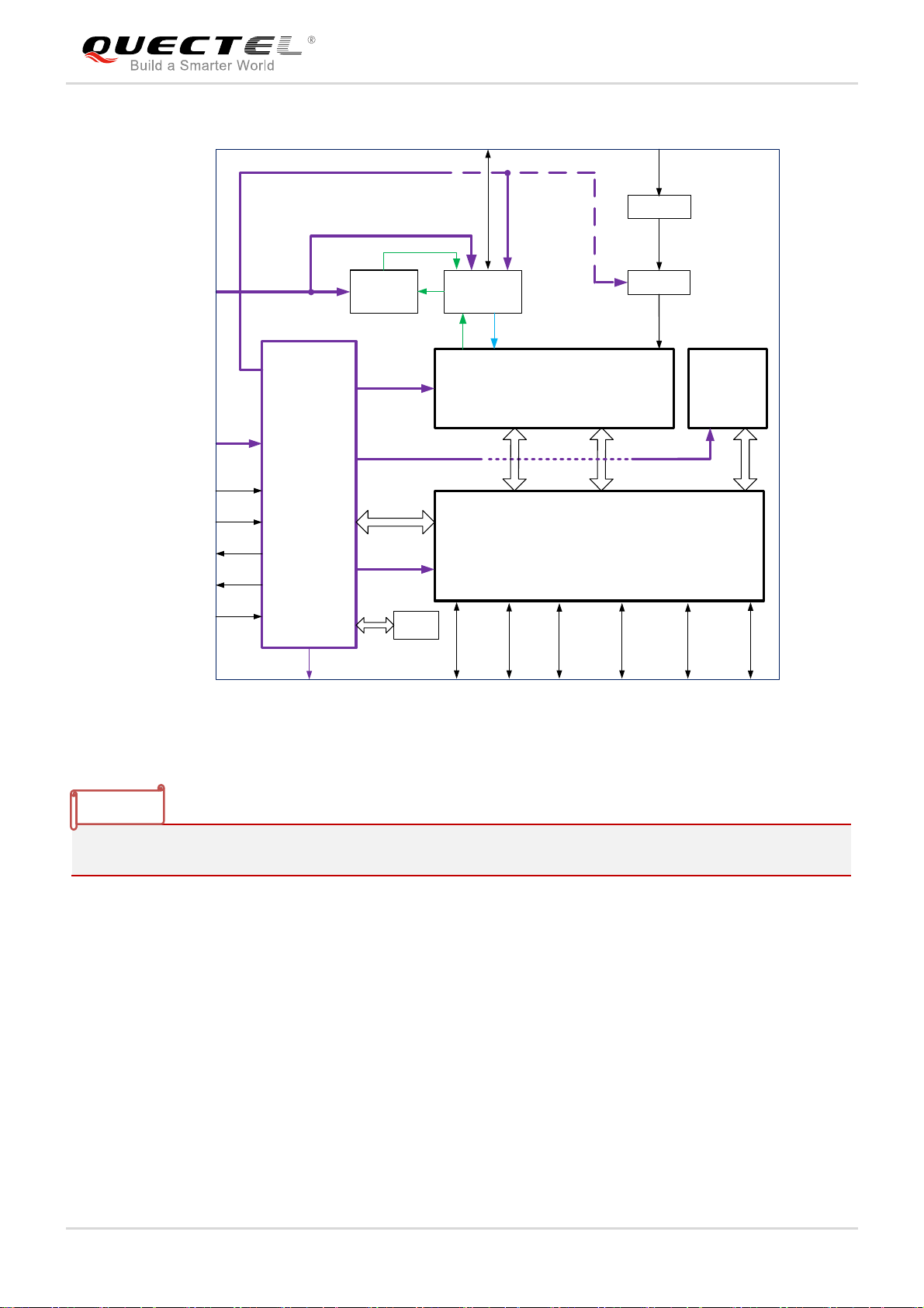
LTE Module Series
BG96 Hardware Design
VBAT_RF
VBAT_BB
PWRKEY
RESET_N
STATUS
NETLIGHT
PMIC
PA
(4G)
Control
ANT_MAIN
PA
(2G+ASM)
Tx
ANT_GNSS
Rx
GNSS
Transceiver
IQ Control
Baseband
SAW
LNA
NAND
DDR2
SDRAM
ADCs
VDD_EXT
19.2M
XO
USB
(U)SIM PCM*
UARTs
I2C*
GPIOs
Figure 1: Functional Diagram
NOTE
“*” means under development.
2.4. Evaluation Board
In order to help customers develop applications conveniently with BG96, Quectel supplies theevaluation
board (EVB), USB to RS-232converter cable, USB data cable, earphone, antenna and other peripherals
to control or test the module. For more details, please refer to document [1].
BG96_Hardware_Design 18 / 81
Page 20

LTE Module Series
BG96 Hardware Design
BG96_Hardware_Design 19 / 81
Page 21
LTE Module Series
BG96 Hardware Design
3 Application Interfaces
BG96is equipped with 102 LGA pads that can be connected to customers’ cellular application platforms.
The following sub-chapters will provide detailed description of interfaces listed below:
Power supply
(U)SIMinterface
USB interface
UART interfaces
PCM* and I2C* interfaces
Status indication
USB_BOOT interface
ADC interfaces
GPIO interfaces
NOTE
“*” means under development.
BG96_Hardware_Design 20 / 81
Page 22

LTE Module Series
BG96 Hardware Design
3.1. Pin Assignment
The following figure showsthe pin assignment of BG96.
BG96_Hardware_Design 21 / 81
Page 23
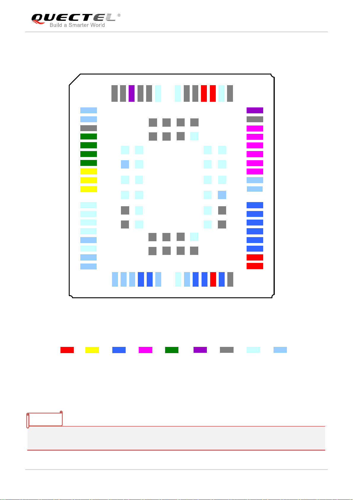
LTE Module Series
BG96 Hardware Design
PS M_I ND
ADC 1
GND
PCM _C LK*
PCM _SY N C*
PCM _I N*
PCM _OU T*
USB_VBUS
USB_DP
USB_DM
RESERVED
RESERVED
RESERVED
RESERVED
PW RKEY
RESERVED
RESET_N
W_ DI SABL E#
62
ANT _M AIN
GND
GND
59
60
61
RESERVED
GND
GND
58
57
56
RESERVED
55
GND
GND
53
54
1
2
82 81
80 79
3
4
10 2 10 1
10 0
99
5
63
6
7
GPIO64
83
64
84
98
97
8
65
9
85
96
10
66
86
95
11
12
13
87
68
88
94
93
67
14
1)
15
16
89 90
69
91 92
71
70
72
17
18
RESERVED
VB AT_ RF
VB AT_ RF
GND
50
51
52
78
77
76
USB_BOOT
75
74
73
49
48
47
46
45
44
43
42
41
40
39
38
37
36
35
34
33
32
ANT _G NSS
GND
USIM_GND
USIM_CLK
USIM_DATA
USIM_RST
USIM_VDD
USIM_PRESENCE
I2C_SDA*
I2C_SCL*
RI
DCD
RTS
CTS
TXD
RXD
VB AT_ BB
VB AT_ BB
27
19
AP _REA D Y
PO WER USB UART
20
ST ATU S
21
NETLIGHT
22
DBG_RXD
(U)SIM
23
DBG_TXD
24
ADC0
PCM
25
RESERVED
26
GPIO 26
UART3_TXD
ANT
Figure 2: Pin Assignment (Top View)
NOTES
1. Keep all RESERVEDpins and unused pins unconnected.
2. GND pads should be connected to ground in the design.
28
UART3_RXD
29
VDD _EX T
30
DTR
GND
31
GND
RESERVED
OTHE RS
BG96_Hardware_Design 22 / 81
Page 24
LTE Module Series
BG96 Hardware Design
3. 1)PWRKEY output voltage is 0.8V because of the diode drop in the Qualcomm chipset.
4. “*” means under development.
3.2. Pin Description
The following tables show the pin definition and description of BG96.
Table 3: Definition of I/O Parameters
Type Description
IO Bidirectional
DI Digital input
DO Digital output
PI Power input
PO Power output
AI Analog input
AO Analog output
OD Open drain
Table 4: Pin Description
Power Supply
Pin Name Pin No. I/O Description
Power supply
VBAT_BB 32, 33 PI
VBAT_RF 52,53 PI
BG96_Hardware_Design 23 / 81
for the
module’s
baseband part
Power supply
for the
DC
Characteristics
Vmax=4.3V
Vmin=3.3V
Vnorm=3.8V
Vmax=4.3V
Vmin=3.3V
Comment
Page 25
LTE Module Series
BG96 Hardware Design
module’s RF
part
Provide 1.8V
VDD_EXT 29 PO
for external
circuit
3, 31, 48,
50, 54, 55,
58, 59, 61,
GND
62, 67~74,
Ground
79~82,
89~91,
100~102
Turn on/off
Pin Name Pin No. I/O Description
PWRKEY 15 DI
Turnon/off the
module
Vnorm=3.8V
Vnorm=1.8V
I
max=50mA
O
DC
Characteristics
Vnorm=0.8V
V
max=0.5V
IL
Power supply for external
GPIO’s pull-up circuits.
Comment
The output voltage
is0.8V because of
thediode drop in
theQualcomm chipset.
RESET_N 17 DI
Resetthe
module
Status Indication
Pin Name Pin No. I/O Description
Indicate the
STATUS 20 DO
module’soperat
ionstatus
Indicate the
NETLIGHT 21 DO
module’snetwor
k activity status
USB Interface
Pin Name Pin No. I/O Description
USB_VBUS 8 PI USB detection
V
max=2.1V
IH
V
min=1.3V
IH
V
max=0.5V
IL
DC
Characteristics
V
min=1.35V
OH
V
max=0.45V
OL
V
min=1.35V
OH
V
max=0.45V
OL
DC
Characteristics
Vmax=5.25V
Vmin=3.0V
If unused, keep this pin
open.
Comment
1.8V power domain.
If unused, keep this pin
open.
1.8V power domain.
If unused, keep this pin
open.
Comment
USB_DP 9 IO
USB differential
data bus(+)
BG96_Hardware_Design 24 / 81
Vnorm=5.0V
Compliant with
USB 2.0 standard
specification.
Require differential
impedance of 90Ω.
Page 26

LTE Module Series
BG96 Hardware Design
USB_DM 10 IO
USB differential
data bus (-)
(U)SIM Interface
Pin Name Pin No. I/O Description
USIM_
PRESENCE
42 DI
USIM_VDD 43 PO
(U)SIM card
insertion
detection
Power supply
for (U)SIM card
Compliant with
USB 2.0 standard
specification.
DC
Characteristics
V
min=-0.3V
IL
V
max=0.6V
IL
V
min=1.2V
IH
V
max=2.0V
IH
For 1.8V(U)SIM:
Vmax=1.9V
Vmin=1.7V
For 3.0V(U)SIM:
Vmax=3.05V
Vmin=2.7V
IOmax=50mA
Require differential
impedance of 90Ω.
Comment
1.8V power domain.
If unused, keep this pin
open.
Either 1.8V or 3.0V is
supported by the module
automatically.
USIM_RST 44 DO
USIM_DATA 45 IO
USIM_CLK 46 DO
Reset signal of
(U)SIM card
Data signal of
(U)SIM card
Clock signal of
(U)SIM card
For 1.8V (U)SIM:
V
max=0.45V
OL
V
min=1.35V
OH
For 3.0V (U)SIM:
max=0.45V
V
OL
V
min=2.55V
OH
For 1.8V (U)SIM:
V
max=0.6V
IL
V
min=1.2V
IH
V
max=0.45V
OL
V
min=1.35V
OH
For 3.0V (U)SIM:
max=1.0V
V
IL
V
min=1.95V
IH
V
max=0.45V
OL
V
min=2.55V
OH
For 1.8V (U)SIM:
V
max=0.45V
OL
V
min=1.35V
OH
For 3.0V (U)SIM:
max=0.45V
V
OL
V
min=2.55V
OH
BG96_Hardware_Design 25 / 81
Page 27
BG96 Hardware Design
USIM_GND 47
UART1 Interface
Specified
ground for
(U)SIM card
LTE Module Series
Pin Name Pin No. I/O Description
Data terminal
DTR 30 DI
ready(sleepmo
de control)
RXD 34 DI Receive data
TXD 35 DO Transmit data
CTS 36 DO Clear to send
RTS 37 DI
DCD 38 DO
Request to
send
Data carrier
detection
DC
Characteristics
V
min=-0.3V
IL
V
max=0.6V
IL
V
min=1.2V
IH
V
max=2.0V
IH
V
min=-0.3V
IL
V
max=0.6V
IL
V
min=1.2V
IH
V
max=2.0V
IH
V
max=0.45V
OL
V
min=1.35V
OH
V
max=0.45V
OL
V
min=1.35V
OH
V
min=-0.3V
IL
V
max=0.6V
IL
V
min=1.2V
IH
V
max=2.0V
IH
V
max=0.45V
OL
V
min=1.35V
OH
Comment
1.8V power domain.
If unused, keep this pin
open.
1.8V power domain.
If unused, keep this pin
open.
1.8V power domain.
If unused, keep this pin
open.
1.8V power domain.
If unused, keep this pin
open.
1.8V power domain.
If unused, keep this pin
open.
1.8V power domain.
If unused, keep this pin
open.
RI 39 DO Ring indicator
UART2 Interface
Pin Name Pin No. I/O Description
DBG_RXD 22 DI Receive data
DBG_TXD 23 DO Transmit data
UART3 Interface
BG96_Hardware_Design 26 / 81
V
max=0.45V
OL
V
min=1.35V
OH
DC
Characteristics
V
min=-0.3V
IL
V
max=0.6V
IL
V
min=1.2V
IH
V
max=2.0V
IH
V
max=0.45V
OL
V
min=1.35V
OH
1.8V power domain.
If unused, keep this pin
open.
Comment
1.8V power domain.
If unused, keep this pin
open.
1.8V power domain.
If unused, keep this pin
open.
Page 28
LTE Module Series
BG96 Hardware Design
Pin Name Pin No. I/O Description
UART3_TXD
27 DO
Transmit data
UART3_RXD 28 DI Receive data
PCM* Interface
Pin Name Pin No. I/O Description
PCM_CLK* 4 DO
PCMclock
output
PCMframe
PCM_SYNC* 5 DO
synchronization
output
DC
Characteristics
V
max=0.45V
OL
V
min=1.35V
OH
V
min=-0.3V
IL
V
max=0.6V
IL
V
min=1.2V
IH
V
max=2.0V
IH
DC
Characteristics
V
max=0.45V
OL
V
min=1.35V
OH
V
max=0.45V
OL
V
min=1.35V
OH
Comment
1.8V power domain.
If unused, keep this pin
open.
1.8V power domain.
If unused, keep this pin
open.
Comment
1.8V power domain.
If unused, keep this pin
open.
1.8V power domain.
If unused, keep this pin
open.
PCM_IN* 6 DI
PCM_OUT* 7 DO
PCMdata input
PCMdata
output
I2C* Interface
Pin Name Pin No. I/O Description
I2C serial clock.
I2C_SCL* 40 OD
Used for
external codec.
V
min=-0.3V
IL
V
max=0.6V
IL
V
min=1.2V
IH
V
max=2.0V
IH
V
max=0.45V
OL
V
min=1.35V
OH
DC
Characteristics
1.8V power domain.
If unused, keep this pin
open.
1.8V power domain.
If unused, keep this pin
open.
Comment
External pull-up resistor
is required.
1.8V only.
If unused, keep
this pin open.
I2C serial data.
I2C_SDA* 41 OD
Used for
external codec.
BG96_Hardware_Design 27 / 81
External pull-up resistor
is required.
1.8V only.
If unused, keep this pin
open.
Page 29
Antenna Interfaces
LTE Module Series
BG96 Hardware Design
Pin Name Pin No. I/O Description
ANT_MAIN 60 IO
ANT_GNSS 49 AI
Main antenna
interface
GNSS antenna
interface
Other Pins
Pin Name Pin No. I/O Description
PSM_IND1) 1 DO
W_DISABLE# 18 DI
Power saving
mode indicator
Airplane mode
control
DC
Characteristics
Comment
50Ωimpedance
50Ωimpedance
DC
Characteristics
V
max=0.45V
OL
V
min=1.35V
OH
If unused, keep this pin
open.
Comment
1.8V power domain.
If unused, keep this pin
open.
1.8V power domain.
V
min=-0.3V
IL
V
max=0.6V
IL
V
min=1.2V
IH
V
max=2.0V
IH
Pull-up by default.
In low voltage level, the
module can enter into
airplane mode.
If unused, keep this pin
open.
Application
AP_READY 19 DI
processor
sleep state
detection
Force the
module to enter
USB_BOOT 75 DI
into emergency
download
mode
General-
GPIO26 26 IO
purpose input/
output interface
General-
purpose input/
GPIO64 64 IO
output
interface
V
min=-0.3V
IL
V
max=0.6V
IL
V
min=1.2V
IH
V
max=2.0V
IH
V
min=-0.3V
IL
V
max=0.6V
IL
V
min=1.2V
IH
V
max=2.0V
IH
V
max=0.45V
OL
V
min=1.35V
OH
V
min=-0.3V
IL
V
max=0.6V
IL
V
min=1.2V
IH
V
max=2.0V
IH
VOLmax=0.45V
V
min=1.35V
OH
V
min=-0.3V
IL
V
max=0.6V
IL
V
min=1.2V
IH
V
max=2.0V
IH
1.8V power domain.
If unused, keep this pin
open.
1.8V power domain.
If unused, keep this pin
open.
1.8V power domain.
If unused, keep this pin
open.
1.8V power domain.
If unused, keep this pin
open.
BG96_Hardware_Design 28 / 81
Page 30

ADC Interfaces
LTE Module Series
BG96 Hardware Design
Pin Name Pin No. I/O Description
General
purpose analog
ADC1 2 AI
ADC0 24 AI
RESERVED Pins
Pin Name Pin No. I/O Description
11~14, 16,
to digital
converter
interface
General
purpose analog
to digital
converter
interface
25, 51,
DC
Characteristics
Voltage range:
0.3V to 1.8V
Voltage range:
0.3V to 1.8V
DC
Characteristics
Comment
If unused, keep this pin
open.
If unused, keep this pin
open.
Comment
56, 57,
RESERVED
63,
Reserved
Keep these pins open.
65,66,
76~78,
83~88,
92~99
NOTES
1. “*” means under development.
1)
2.
When PSM is enabled and then reboot the module, the function of PSM_IND pin will be activated.
This pin outputs a high level voltage when the module is in normal operation state, and outputs a low
level voltage when the module enters into PSM.
3. Keep all RESERVED pins and unused pins unconnected.
BG96_Hardware_Design 29 / 81
Page 31

LTE Module Series
BG96 Hardware Design
3.3. Operating Modes
The table below briefly summarizes the various operating modes referred in the following chapters.
Table 5: Overview of Operating Modes
Mode Details
Normal
Operation
Extended Idle
Mode DRX
(e-I-DRX)
Airplane
Mode
Minimum
Functionality
Mode
Sleep Mode
Talk/Data
Idle
BG96 module and the network may negotiate over non-access stratum signaling the
use of e-I-DRX for reducing power consumption, while being available for mobile
terminating data and/or network originated procedures within a certain delay dependent
on the DRX cycle value.
AT+CFUN command or W_DISABLE# pin can set the module into airplane mode. In
this case, RF function will be invalid.
AT+CFUN command can set the module into a minimum functionality mode without
removing the power supply. In this case, both RF function and (U)SIM card will be
invalid.
In this mode, the current consumption of the module will be reduced to a lower level.
During this mode, the module can still receive paging message, SMS and TCP/UDP
data from the network normally.
Network connection is ongoing. In this mode, the power consumption is
decided by network settingand data transfer rate.
Software is active. The module hasregistered onnetwork, and it is
ready to send and receive data.
BG96 module may enter into Power Saving Mode for reducing its
Power Saving
Mode
(PSM)
power consumption. PSM is similar to power-off, but the module
remains registered on the network and there is no need to
re-attach or re-establish PDN connections.
Power OFF
Mode
In this mode, the power management unit shuts down the power supply. Software is not
active. The serial interfacesare not accessible. Butoperating voltage (connected to
VBAT_RF and VBAT_BB) remains applied.
NOTES
BG96_Hardware_Design 30 / 81
Page 32

LTE Module Series
BG96 Hardware Design
During e-I-DRX, it is recommended to use UART interface for data
communication, as the use of USB interface will increase power consumption.
3.4. Power Saving
3.4.1. Airplane Mode
When the module enters into airplane mode, the RF function does not work, and all AT commands
correlative with RF function will be inaccessible. This mode can be set via the following ways.
Hardware:
W_DISABLE# is pulled up by default.Driving it to low level will let the module enter into airplane mode.
Software:
AT+CFUN=<fun>command provides choice of the functionality level, through setting <fun> into 0, 1 or 4.
AT+CFUN=0: Minimum functionality mode. Both (U)SIM and RF functions are disabled.
AT+CFUN=1: Full functionality mode (by default).
AT+CFUN=4: Airplane mode. RF function is disabled.
NOTES
1. Airplane mode control viaW_DISABLE# is disabled in firmware by default. It can be enabled by
AT+QCFG=“airplanecontrol” command.
2. The execution of AT+CFUN command will not affect GNSS function.
3.4.2. Power Saving Mode(PSM)
BG96 module can enter into PSM for reducing its power consumption. The
BG96_Hardware_Design 31 / 81
Page 33

LTE Module Series
BG96 Hardware Design
mode is similar to power-off, but the module remains registered on the network
and there is no need to re-attach or re-establish PDN connections.So BG96 in
PSM cannot immediately respond users’ requests.
When the module wants to use the PSM it shall request an Active Time value
during every Attach and TAU procedures. If the network supports PSM and
accepts that the module uses PSM, the network confirms usage of PSM by
allocating an Active Time value to the module. If the module wants to change
the Active Time value, e.g. when the conditions are changed in the module, the
module consequently requests the value it wants in the TAU procedure.
If PSM is supported by the network, then it can be enabled via AT+CPSMScommand.
Either of the following methods will wake up the module from PSM:
Drive PWRKEY pin to low level will wake up the module.
When the T3412_Exttimer expires, the module will be automatically woken up.
NOTE
Please refer to document [2] for details about A T+CPSMScommand.
3.4.3. Extended Idle Mode DRX(e-I-DRX)
The module (UE) and the network may negotiate over non-access stratum
signalling the use of e-I-DRX for reducing its power consumption, while being
available for mobile terminating data and/or network originated procedures
BG96_Hardware_Design 32 / 81
Page 34

LTE Module Series
BG96 Hardware Design
within a certain delay dependent on the DRX cycle value.
Applications that want to use e-I-DRX need to consider specific handling of
mobile terminating services or data transfers, and in particular they need to
consider the delay tolerance of mobile terminated data.
In order to negotiate the use of e-I-DRX, the UE requests e-I-DRXparameters
during attach procedure and RAU/TAU procedure. The EPC may reject or
accept the UE request for enabling e-I-DRX. In case the EPC accepts e-I-DRX,
the EPC based on operator policies and, if available, the e-I-DRXcycle length
value in the subscription data from the HSS, may also provide different values
of the e-I-DRXparameters than what was requested by the UE. If the EPC
accepts the use of e-I-DRX, the UE applies e-I-DRX based on the received
e-I-DRXparameters. If the UE does not receive e-I-DRXparameters in the
relevant accept message because the EPC rejected its request or because the
request was received by EPC not supporting e-I-DRX, the UE shall apply its
regular discontinuous reception.
Ife-I-DRX is supported by the network, then it can be enabled by
AT+CEDRXS=1command.
NOTE
BG96_Hardware_Design 33 / 81
Page 35

LTE Module Series
BG96 Hardware Design
Please refer to document [2] for details about AT+CEDRXScommand.
3.4.4. Sleep Mode
BG96 is able to reduce its current consumption to a lower value during the sleep mode. The following
sub-chapters describe the power saving procedure of BG96 module.
3.4.4.1. UART Application
If the host communicates with module via UART interface, the following preconditions can let the module
enter into sleep mode.
Execute AT+QSCLK=1command to enable sleep mode.
Drive DTR to high level.
The following figure shows the connection between the module and the host.
Figure 3: Sleep Mode Application via UART
Driving the host DTR to low level will wake up the module.
When BG96 has URC to report, RI signal will wake up the host. Please refer to Chapter 3.14 for
details about RI behavior.
AP_READY will detect the sleep state of the host (can be configured to high level or low level
detection). Please refer to AT+QCFG=“apready” command in document [2] for details.
BG96_Hardware_Design 34 / 81
Page 36

LTE Module Series
BG96 Hardware Design
3.5. Power Supply
3.5.1. Power Supply Pins
BG96 provides the following four VBAT pins for connection with anexternal power supply. There are two
separate voltage domains for VBAT.
Two VBAT_RF pins for module’sRF part.
Two VBAT_BB pins for module’s baseband part.
The following table shows the details of VBAT pins and ground pins.
Table 6: VBAT and GND Pins
Pin Name Pin No. Description Min. Typ. Max. Unit
VBAT_RF 52,53
VBAT_BB 32,33
3, 31, 48,50, 54,
55,58, 59, 61,62,
GND
67~74,
79~82,89~91,100
~102
Power supply for the
module’s RF part
Power supply for the
module’s baseband part
Ground - - - -
3.3 3.8 4.3 V
3.3 3.8 4.3 V
3.5.2. Decrease Voltage Drop
The power supply range of the module is from 3.3Vto4.3V. Please make sure that the input voltage will
never drop below 3.3V.The following figure shows the voltage drop during burst transmission in 2G
network. The voltage drop will be less in LTE CatM1 and LTE CatNB1 networks.
BG96_Hardware_Design 35 / 81
Page 37

LTE Module Series
BG96 Hardware Design
Figure 4: Power Supply Limits during Burst Transmission
To decrease voltage drop, a bypass capacitor of about 100µF with low
ESRshould be used, and a multi-layer ceramic chip capacitor (MLCC) array
should also be reserved due to its low ESR.It is recommended to use three
ceramic capacitors (100nF, 33pF, 10pF) for composing the MLCC array, and
place these capacitors close to VBAT pins.The main power supply from an
external application has to be a single voltage source and can be expanded to
two sub paths with star structure. The width of VBAT_BB trace should be no
less than 0.5mm, and the width of VBAT_RF trace should be no less than 2mm.
In principle, the longer the VBAT trace is, the wider it will be.
In addition, in order to get a stable power source, it is suggested to use a TVS with suitable reverse
stand-off voltageand lower leakage current. and place it as close to the VBATpins as possible. The
following figure shows the star structure of the power supply.
BG96_Hardware_Design 36 / 81
Page 38

LTE Module Series
VB AT
D1
TVS
BG96 Hardware Design
VB AT_ RF
VB AT_BB
C1
100uF
+
C2
100nF
33pF
C3
C4
10pF
C5
100uF
+
C6 C7 C8
100nF
33pF
10pF
Mod ule
Figure 5: Star Structure of the Power Supply
3.5.3. Monitor the Power Supply
AT+CBC command can be usedto monitor the VBAT_BB voltage value. For more details, please refer to
document [2].
3.6. Turn on and off Scenarios
3.6.1. Turn on Module Using the PWRKEY Pin
The following table shows the pin definition of PWRKEY.
Table 7: Pin Definition of PWRKEY
Pin Name Pin No. Description DC Characteristics Comment
The output voltage is0.8V
because of thediode drop
in theQualcomm chipset.
PWRKEY 15 Turn on/off the module
Vnorm=0.8V
V
max=0.5V
IL
When BG96 is in power off mode, it can be turned on to normal mode by
driving the PWRKEY pin to a low level for at least 500ms. It is recommended to
BG96_Hardware_Design 37 / 81
Page 39

LTE Module Series
BG96 Hardware Design
use an open drain/collector driver to control the PWRKEY.After STATUS pin
outputting a high level, PWRKEY pin can be released. A simple reference
circuit is illustrated in the following figure.
PWRKEY
≥500ms
4.7K
Turn on pulse
47K
10nF
Figure 6: Turn on the Module Using Driving Circuit
Another way to control the PWRKEY is using a button directly. When pressing the key, electrostatic strike
may generate from the finger. Therefore, aTVS component is indispensable to be placed nearby the
button for ESD protection. A reference circuit is shownin the following figure.
Figure 7: Turn on the Module Using Keystroke
The turn on scenario is illustrated in the following figure.
BG96_Hardware_Design 38 / 81
Page 40

LTE Module Series
BG96 Hardware Design
NOTE
VBAT
PWRKEY
RESET _N
STATUS
(DO)
USB
URAT
≥500ms
VIL≤0.5V
Inactive
Inactive
≥ 4.8s
≥ 4.2s
Act ive
≥ 4.9s
Act ive
Figure 8: Timing of Turning on Module
NOTE
1. Make sure that VBAT is stable before pulling down PWRKEY pin. The time between them is no less
than 30ms.
2. Customers should expect to see ~0.8V on the PWRKEY pin, because of there is pulled up to an
internal voltage minus a diode drop in the Qualcomm chipset.
3.6.2. Turn off Module
Either of the following methods can be used to turn off the module:
Normal power down procedure: Turn off the module using the PWRKEY pin.
Normal power down procedure: Turn off the module using AT+QPOWDcommand.
3.6.2.1. Turn off Module Using the PWRKEY Pin
Driving the PWRKEY pin to a low level voltagefor at least 650ms, the module will execute power-down
procedure after the PWRKEY is released.
The power-down scenario is illustrated inthe following figure.
BG96_Hardware_Design 39 / 81
Page 41

LTE Module Series
BG96 Hardware Design
Figure 9: Timing of Turning off Module
3.6.2.2. Turn off Module Using AT Command
It is also a safe way to use AT+QPOWDcommandto turn off the module, which is similar to turning off the
module via PWRKEY pin.
Please refer todocument [2] for details about AT+QPOWDcommand.
3.7. Reset the Module
The RESET_N pin can be used to reset the module.The module can be reset by driving RESET_N to a
low level voltage for time between 150ms and 460ms.
Table 8: RESET_N Pin Description
Pin Name Pin No. Description DC Characteristics Comment
V
max=2.1V
IH
V
min=1.3V
IH
V
max=0.5V
IL
RESET_N 17
Resetsignal of the
module
The recommended circuit is similar to the PWRKEY control circuit. An open drain/collector driver or button
can be used to control the RESET_N.
BG96_Hardware_Design 40 / 81
Page 42

LTE Module Series
BG96 Hardware Design
Figure 10: Reference Circuit of RESET_N by Using Driving Circuit
Figure 11: Reference Circuit of RESET_N by Using Button
The reset scenario is illustrated inthe following figure.
BG96_Hardware_Design 41 / 81
Page 43

NOTES
LTE Module Series
BG96 Hardware Design
Figure 12: Timing of Resetting Module
1. Use RESET_N only when turning off the module by AT+QPOWDcommand and PWRKEY pin both
failed.
Ensure that there is no large capacitance on PWRKEY and RESET_N pins.
3.8. (U)SIM Interface
The(U)SIM interface circuitrymeets ETSI and IMT-2000 requirements. Both 1.8V and 3.0V (U)SIM cards
are supported.
Table 9: Pin Definition of (U)SIM Interface
Pin Name Pin No. I/O Description Comment
USIM_
PRESENCE
42 DI (U)SIM card insertion detection
USIM_VDD 43 PO Power supply for (U)SIM card
USIM_RST 44 DO Reset signal of (U)SIM card
USIM_DATA 45 IO Data signal of (U)SIM card
USIM_CLK 46 DO Clock signal of (U)SIM card
USIM_GND 47 Specified ground for (U)SIM card
BG96_Hardware_Design 42 / 81
Either 1.8V or 3.0V is supported
by the module automatically.
Page 44

LTE Module Series
BG96 Hardware Design
BG96 supports (U)SIM card hot-plug via the USIM_PRESENCEpin. The
function supports low level and high level detections, andisdisabled by default.
Please refer to document [2] about AT+QSIMDETcommand for details.
The following figure shows a reference design of (U)SIM interface with an 8-pin
(U)SIM cardconnector.
Figure 13: Reference Circuit of (U)SIM Interface withan 8-Pin (U)SIM Card Connector
If (U)SIM card detection function is not needed, please keep USIM_PRESENCE unconnected.
Areference circuit for (U)SIM interface with a 6-pin (U)SIM card connector is illustrated inthe following
figure.
BG96_Hardware_Design 43 / 81
Page 45

LTE Module Series
BG96 Hardware Design
Figure 14: Reference Circuit of (U)SIM Interface with a 6-Pin (U)SIM Card Connector
In order to enhance the reliability and availability of the (U)SIM card in
applications, please follow the criteria below in (U)SIM circuit design:
Keep placement of (U)SIM card connector as close to the module as possible. Keep the trace length
as less than 200mm as possible.
Keep (U)SIM card signals away from RF and VBAT traces.
Assure the ground between the module and the (U)SIM card connector short and wide. Keep the
trace width of ground and USIM_VDD no less than 0.5mm to maintain the same electric potential.
Make sure the bypass capacitor between USIM_VDD and USIM_GND less than 1uF, and place it as
close to (U)SIM card connector as possible. If the system ground plane is complete, USIM_GND can
be connected to the systemground directly.
To avoid cross-talk between USIM_DATA and USIM_CLK, keep them awayfromeach other and
shield them with surrounded ground. USIM_RST should also be ground shielded.
In order to offer good ESD protection, it is recommended to add a TVSdiode array with parasitic
capacitance not exceeding15pF. In order to facilitate debugging, it is recommended to reserve series
resistors for the (U)SIM signals of the module.The 33pFcapacitors are used for filtering interference
of GSM900MHz.Please note that the (U)SIM peripheral circuit should be close to the (U)SIM
cardconnector.
The pull-up resistor on USIM_DATA line can improve anti-jamming capability when long layout trace
and sensitive occasion areapplied, and should be placed close to the (U)SIM cardconnector.
BG96_Hardware_Design 44 / 81
Page 46

LTE Module Series
BG96 Hardware Design
3.9. USB Interface
BG96 contains one integrated Universal Serial Bus (USB) interfacewhich complies with the USB 2.0
specification and supports high-speed (480Mbps) and full-speed (12Mbps)modes. The USB interface is
used for AT command communication, data transmission, software debugging and firmware upgrade. The
following table shows the pin definition of USB interface.
Table 10: Pin Definitionof USB Interface
Pin Name Pin No. I/O Description Comment
USB_VBUS 8 PI USB connection detection Typically 5.0V
USB_DP 9 IO USB differential data bus (+)
USB_DM 10 IO USB differential data bus (-)
Require differential
impedance of 90Ω
Require differential
impedance of 90Ω
GND 3 Ground
For more details about USB 2.0 specification, please visithttp://www.usb.org/home
.
The USB interface is recommended to be reserved for firmware upgrade in customers’designs. The
following figure shows areference circuit of USB interface.
Figure 15: Reference Circuit of USB Interface
A common mode choke L1 is recommended to be added in series between the module and customer’s
MCU in order to suppress EMI spurious transmission. Meanwhile, the 0Ω resistors (R3 and R4) should be
BG96_Hardware_Design 45 / 81
Page 47

LTE Module Series
BG96 Hardware Design
added in series between the module and the test points so as to facilitate debugging, and the resistors are
not mounted by default. In order to ensure the integrity of USB data line signal, L1/R3/R4 components
must be placed close to the module, and also these resistors should be placed close to each other. The
extra stubs of trace must be as short as possible.
The following principles should be complied with when design the USB interface, so as to meet USB 2.0
specification.
It is important to route the USB signal traces as differential pairs with total grounding. The impedance
of USB differential trace is 90Ω.
Do not route signal traces under crystals, oscillators, magnetic devices and RF signal traces. It is
important to route the USB differential traces in inner-layer with ground shielding onnot only upper
and lower layers but also right and left sides.
Pay attention to the influence of junction capacitance of ESD protection components on USB data
lines. Typically, the capacitance value should be less than 2pF.
Keep the ESD protection componentsas close to the USB connector as possible.
NOTE
BG96 module can only be used as a slave device.
3.10. UART Interfaces
The module provides threeUART interfaces: UART1,UART2 and UART3interfaces. The following are
theirfeatures.
UART1 interface supports
9600bps,19200bps,38400bps,57600bps,115200bps,230400bps,460800bps and921600bpsbaud
rates, and the default is 115200bps. Itis used for data transmission and AT command
communication.
UART2 interface supports 115200bpsbaud rate, and is used formodule debugging and log output.
UART3interface supports 115200bps baud rate, and is used for outputting GNSS dataandNMEA
sentences.
The following tables show the pin definition of the three UART interfaces.
BG96_Hardware_Design 46 / 81
Page 48

BG96 Hardware Design
Table 11: Pin Definition of UART1Interface
Pin Name Pin No. I/O Description Comment
LTE Module Series
DTR 30 DI
RXD 34 DI Receive data 1.8V power domain
TXD 35 DO Transmit data 1.8V power domain
CTS 36 DO Clear to send 1.8V power domain
RTS 37 DI Request to send 1.8V power domain
DCD 38 DO Data carrier detection 1.8V power domain
RI 39 DO Ring indicator 1.8V power domain
Data terminal ready.
Sleepmode control
1.8V power domain
Table 12: Pin Definition of UART2Interface
Pin Name Pin No. I/O Description Comment
DBG_RXD 22 DI Receive data 1.8V power domain
DBG_TXD 23 DO Transmit data 1.8V power domain
Table 13: Pin Definition of UART3Interface
Pin Name Pin No. I/O Description Comment
UART3_TXD 27 DO Transmit data 1.8V power domain
UART3_RXD 28 DI Receive data 1.8V power domain
The logic levels are described in the following table.
BG96_Hardware_Design 47 / 81
Page 49

LTE Module Series
BG96 Hardware Design
Table 14:Logic Levels of Digital I/O
Parameter Min. Max. Unit
VIL -0.3 0.6 V
VIH 1.2 2.0 V
VOL 0 0.45 V
VOH 1.35 1.8 V
The module provides 1.8V UART interface. A level translator should be used if
customers’application is equipped with a 3.3V UART interface. A level
translator TXS0108EPWR provided by Texas Instrumentsis recommended.
The following figure shows a reference design.
Figure 16: Reference Circuit with Translator Chip
Please visit http://www.ti.com
formore information.
Another example with transistor translation circuit is shown as below.
Thecircuitdesign of dotted line section can refer to thatof solid line section, in
BG96_Hardware_Design 48 / 81
Page 50

LTE Module Series
BG96 Hardware Design
terms of both module input and output circuit designs, but please pay attention
to the direction of connection.
Figure 17: Reference Circuit with Transistor Circuit
NOTE
Transistor circuit solution is not suitable for applications with high baud rates exceeding 460Kbps.
3.11. PCM* and I2C* Interfaces
BG96 provides one Pulse Code Modulation (PCM)digital interface and one I2C interface. The following
table shows the pin definition of the two interfaces which can be applied on audio codec design.
Table 15: Pin Definition of PCM and I2C Interfaces
Pin Name Pin No. I/O Description Comment
PCM_CLK* 4 DO PCM clock output 1.8V power domain
PCM_SYNC* 5 DO
BG96_Hardware_Design 49 / 81
PCMframe synchronization
output
1.8V power domain
Page 51
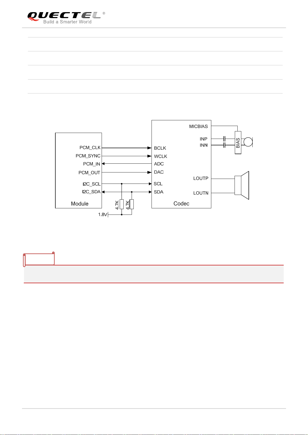
LTE Module Series
BG96 Hardware Design
PCM_IN* 6 DI PCM data input 1.8V power domain
PCM_OUT* 7 DO PCM dataoutput 1.8V power domain
I2C_SCL* 40 OD I2C serial clock Require external pull-up to 1.8V
I2C_SDA* 41 OD I2C serial data Require external pull-up to 1.8V
The following figure shows a reference design of PCM and I2Cinterfaces with an external codec IC.
Figure 18: Reference Circuit of PCM Application with Audio Codec
NOTE
“*” means under development.
3.12. Network Status Indication
BG96 provides one network status indication pin:NETLIGHT. The pin is used to
drive a network status indication LED. The following tables describe the pin
definition and logic level changes ofNETLIGHT in different network activity
status.
BG96_Hardware_Design 50 / 81
Page 52

LTE Module Series
BG96 Hardware Design
Table 16: Pin Definition of NETLIGHT
Pin Name Pin No. I/O Description Comment
NETLIGHT 21 DO
Indicate the module’snetwork activity
status
1.8V power domain
Table 17: Working State of NETLIGHT
Pin Name Logic Level Changes Network Status
Flicker slowly (200ms High/1800ms Low) Network searching
Flicker slowly (1800ms High/200ms Low) Idle
NETLIGHT
Flicker quickly (125ms High/125ms Low) Data transfer is ongoing
Always high Voice calling
A reference circuit is shown in the following figure.
Figure 19: Reference Circuit of the Network Status Indicator
BG96_Hardware_Design 51 / 81
Page 53

LTE Module Series
BG96 Hardware Design
3.13. STATUS
The STATUS pin is used to indicate the operation status of BG96 module. It will output high level when
the module is poweredon.
The following table describes the pin definition of STATUS.
Table 18: Pin Definition of STATUS
Pin Name Pin No. I/O Description Comment
Indicate the module’s
STATUS 20 DO
operation status
The following figure shows a reference circuit of STATUS.
1.8V power domain
Figure 20: Reference Circuit of STATUS
3.14. Behaviors of RI
AT+QCFG=“risignaltype”,“physical”command can be used to configure RI behavior.
BG96_Hardware_Design 52 / 81
Page 54

LTE Module Series
BG96 Hardware Design
No matter on which port URC is presented, URC will trigger the behavior of RI
pin.
NOTE
URC can be outputted from UART port, USB AT port and USB modem port, through configuration
viaAT+QURCCFGcommand. The default port is USB AT port.
The default behaviors of RI areshown as below.
Table 19:Default Behaviors of RI
State Response
Idle RI keeps in high level.
URC RI outputs 120ms low pulse when new URC returns.
The default RI behaviors can be configured flexibly by AT+QCFG=“urc/ri/ring”command.For more
details, please refer to document [2].
3.15. USB_BOOT Interface
BG96 provides a USB_BOOT pin. During development or factory production,
USB_BOOT can force the module to boot from USB port for firmware upgrade.
BG96_Hardware_Design 53 / 81
Page 55

LTE Module Series
BG96 Hardware Design
Table 20: Pin Definition of USB_BOOT Interface
Pin Name Pin No. I/O Description Comment
1.8V power domain.
USB_BOOT 75 DI
Force the module to enter into
emergency download mode
Active high.
If unused, keep it open.
The following figure shows a reference circuit of USB_BOOT interface.
Figure 21: Reference Circuit of USB_BOOT Interface
NOTE
It is recommended to reserve the above circuit design during application design.
3.16. ADC Interfaces
The module provides two analog-to-digital converter (ADC) interfaces.AT+QADC=0 command can be
used to read the voltage value on ADC0 pin. AT+QADC=1 command can be used to read the voltage
value on ADC1 pin. For more details about these AT commands, please refer todocument [2].
In order to improve the accuracy of ADCvoltage values, the trace of ADC should be surrounded by
ground.
BG96_Hardware_Design 54 / 81
Page 56

LTE Module Series
BG96 Hardware Design
Table 21: Pin Definition of ADCInterfaces
Pin Name Pin No. Description
ADC0 24 General purpose analog to digital converter interface
ADC1 2 General purpose analog to digital converter interface
The following table describes the characteristics of ADC interfaces.
Table 22: Characteristics of ADC Interfaces
Parameter Min. Typ. Max. Unit
ADC0 Voltage Range 0.3 1.8 V
ADC1 Voltage Range 0.3 1.8 V
ADC Resolution 15 bits
ADC Analog-input Bandwidth 100 kHz
ADC Sampling Rate 2.4 MHz
NOTES
1. ADC input voltage must not exceed 1.8V.
2. It is prohibited to supply any voltage to ADC pins when VBAT is removed.
3. It is recommended to use resistor divider circuit for ADC application, andthe divider resistor accuracy
should be no less than 1%.
3.17. GPIOInterfaces
The module provides two general-purpose input and output(GPIO) interfaces. AT+QFWD* command can
be used toconfigure corresponding GPIO pin’s status. For more details about the AT command, please
refer to document [2].
BG96_Hardware_Design 55 / 81
Page 57

LTE Module Series
BG96 Hardware Design
Table 23: Pin Definition of GPIOInterfaces
Pin Name Pin No. Description
GPIO26 26 General purpose input and output interface
GPIO64 64 General purpose input and output interface
The following table describes the characteristics of GPIOinterfaces.
Table 24:Logic Levels of GPIO interfaces
Parameter Min. Max. Unit
VIL -0.3 0.6 V
VIH 1.2 2.0 V
VOL 0 0.45 V
VOH 1.35 1.8 V
NOTE
“*” means under development.
BG96_Hardware_Design 56 / 81
Page 58

LTE Module Series
BG96 Hardware Design
4 GNSS Receiver
4.1. General Description
BG96 includes a fully integrated global navigation satellite system solution that supports Gen8C-Lite of
Qualcomm (GPS, GLONASS, BeiDou/Compass, Galileo and QZSS).
BG96 supports standard NMEA-0183 protocol, and outputs NMEA sentences
at 1Hz data update rate via USBinterface by default.
By default, BG96 GNSS engine is switched off. It has to be switched on via AT
command. For more details about GNSS engine technology and configurations,
please refer to document [3].
4.2. GNSS Performance
The following table shows the GNSS performance of BG96.
Table 25: GNSS Performance
Parameter Description Conditions Typ. Unit
Sensitivity
(GNSS)
BG96_Hardware_Design 57 / 81
Cold start Autonomous -146 dBm
Reacquisition Autonomous -157 dBm
Page 59

LTE Module Series
BG96 Hardware Design
Tracking Autonomous -157 dBm
Autonomous 31 s
XTRA enabled 11.54 s
Autonomous 21 s
XTRA enabled 2.52 s
Autonomous 2.7 s
XTRA enabled 1.82 s
Autonomous
@open sky
< 2.5 m
TTFF
(GNSS)
Accuracy
(GNSS)
Cold start
@open sky
Warm start
@open sky
Hot start
@open sky
CEP-50
NOTES
1. Tracking sensitivity: the lowest GNSS signal value at the antenna port on which the module can keep
on positioning for 3 minutes.
2. Reacquisition sensitivity: the lowest GNSS signal value at the antenna port on which the module can
fix position again within 3 minutes after loss of lock.
3. Cold start sensitivity: the lowest GNSS signal value at the antenna port on which the module fixes
position within 3 minutes after executing cold start command.
4.3. Layout Guidelines
The following layout guidelines should be taken into account in customers designs.
Maximize the distance between GNSS antenna and main antenna.
Digital circuits such as (U)SIM card, USB interface, camera module, display connector and SD card
should be kept away from the antennas.
Use ground vias around the GNSS trace and sensitive analog signal traces to provide coplanar
isolation and protection.
Keep 50Ωcharacteristic impedance for the ANT_GNSS trace.
Please refer to Chapter 5 for GNSS antenna reference design and antenna installation information.
BG96_Hardware_Design 58 / 81
Page 60

LTE Module Series
BG96 Hardware Design
5 Antenna Interfaces
BG96 includes a main antenna interface andaGNSS antennainterface. The antenna portshave an
impedance of 50Ω.
5.1. MainAntenna Interface
5.1.1. Pin Definition
The pin definition of main antenna interface is shown below.
Table 26: Pin Definition of Main Antenna Interface
Pin Name Pin No. I/O Description Comment
ANT_MAIN 60 IO Main antennainterface 50Ωcharacteristicimpedance
5.1.2. Operating Frequency
Table 27: BG96 Operating Frequency
3GPP Band Transmit Receive Unit
LTE-FDD B1 1920~1980 2110~2170 MHz
LTE-FDD B2,
1850~1910 1930~1990 MHz
PCS1900
LTE-FDD
1710~1785 1805~1880 MHz
B3,DCS1800
LTE-FDD B4
BG96_Hardware_Design 59 / 81
1710~1755 2110~2155 MHz
Page 61

LTE Module Series
BG96 Hardware Design
LTE-FDD
824~849 869~894 MHz
B5,GSM850
LTE-FDD
880~915 925~960 MHz
B8,EGSM900
LTE-FDD B12 699~716 729~746 MHz
LTE-FDD B13 777~787 746~756 MHz
LTE-FDD B18 815~830 860~875 MHz
LTE-FDD B19 830~845 875~890 MHz
LTE-FDD B20 832~862 791~821 MHz
LTE-FDD B25 1850~1915 1930~1995 MHz
LTE-FDD B26 814~849 859~894 MHz
LTE-FDD B28 703~748 758~803 MHz
LTE-TDD B39 1880~1920 1880~1920 MHz
Table 28: BG96-M Operating Frequency
3GPP Band Transmit Receive Unit
LTE-FDD B1 1920~1980 2110~2170 MHz
LTE-FDD B2
LTE-FDD B3
1850~1910 1930~1990 MHz
1710~1785 1805~1880 MHz
LTE-FDD B4
LTE-FDD B5
LTE-FDD B8
LTE-FDD B12 699~716 729~746 MHz
BG96_Hardware_Design 60 / 81
1710~1755 2110~2155 MHz
824~849 869~894 MHz
880~915 925~960 MHz
Page 62

LTE Module Series
BG96 Hardware Design
LTE-FDD B13 777~787 746~756 MHz
LTE-FDD B18 815~830 860~875 MHz
LTE-FDD B19 830~845 875~890 MHz
LTE-FDD B20 832~862 791~821 MHz
LTE-FDD B25 1850~1915 1930~1995 MHz
LTE-FDD B26 814~849 859~894 MHz
LTE-FDD B28 703~748 758~803 MHz
LTE-TDD B39 1880~1920 1880~1920 MHz
5.1.3. Reference Design of RF Antenna Interface
Areference design of mainantenna padis shown as below. A π-type matching circuit should be
reservedfor better RF performance, and the π-type matching components (R1/C1/C2) should be placed
as close to the antenna as possible. The capacitors are not mounted by default.
Figure 22: Reference Circuit of RF Antenna Interface
5.1.4. Reference Design of RF Layout
For user’s PCB, the characteristic impedance of all RF traces should be
controlled as 50Ω. The impedance of the RF traces is usually determined by
BG96_Hardware_Design 61 / 81
Page 63

LTE Module Series
BG96 Hardware Design
the trace width (W), the materials’ dielectric constant, the distance between
signal layer and reference ground (H), and the clearance between RF trace
and ground(S). Microstrip line or coplanar waveguide line is typically used in
RF layout for characteristic impedance control. The following are reference
designs of microstrip line or coplanar waveguide linewithdifferent PCB
structures.
Figure 23: Microstrip Line Designon a 2-layer PCB
Figure 24: Coplanar Waveguide Line Design on a 2-layer PCB
BG96_Hardware_Design 62 / 81
Page 64

LTE Module Series
BG96 Hardware Design
Figure 25: Coplanar Waveguide Line Design on a 4-layer PCB (Layer 3 as Reference Ground)
Figure 26: Coplanar Waveguide Line Designon a4-layer PCB (Layer 4 as Reference Ground)
In order to ensure RF performance and reliability, the following principles should be complied with in RF
layout design:
Use impedance simulation tool to control the characteristic impedanceof RF tracesas 50Ω.
The GND pins adjacent to RF pins should not bedesigned as thermal relief pads, and should be fully
connected to ground.
The distance between the RF pinsand the RFconnectorshould be as short as possible, and all the
right angle tracesshould be changed to curved ones.
There should be clearance area under the signal pin of the antenna connector or solder joint.
The reference ground of RF traces should be complete. Meanwhile, adding some ground viasaround
RF traces and the reference ground could help to improve RF performance. The distance between
BG96_Hardware_Design 63 / 81
Page 65

LTE Module Series
BG96 Hardware Design
theground viasand RF traces should be no less than two times the width of RF signal traces (2*W).
For more details about RF layout, please refer to document [4].
5.2. GNSS Antenna Interface
The following tables show the pin definition and frequency specification of GNSS antenna interface.
Table 28: Pin Definition of GNSS Antenna Interface
Pin Name Pin No. I/O Description Comment
ANT_GNSS 49 AI GNSS antennainterface 50Ωimpedance
Table 29: GNSS Frequency
Type Frequency Unit
GPS 1575.42±1.023 MHz
GLONASS 1597.5~1605.8 MHz
Galileo 1575.42±2.046 MHz
BeiDou 1561.098±2.046 MHz
QZSS 1575.42 MHz
A reference design of GNSS antenna interfaceis shown as below.
BG96_Hardware_Design 64 / 81
Page 66

LTE Module Series
BG96 Hardware Design
Figure 27: Reference Circuit of GNSS Antenna Interface
NOTES
1. An external LDO can be selected to supply power according to the active antenna requirement.
2. If the module is designed with a passive antenna, then the VDD circuit is not needed.
5.3. Antenna Installation
5.3.1. Antenna Requirements
The following table shows the requirements on main antennaand GNSS antenna.
BG96_Hardware_Design 65 / 81
Page 67

BG96 Hardware Design
Table 30: Antenna Requirements
Antenna Type Requirements
Frequency range: 1559MHz ~1609MHz
Polarization: RHCP or linear
VSWR: <2 (Typ.)
GNSS1)
Passive antenna gain: >0dBi
Active antenna noise figure: <1.5dB
Active antenna gain: > 0dBi
Active antenna embedded LNA gain: < 17dB
VSWR: ≤2
Efficiency: > 30%
Max Input Power (W): 50
Input Impedance (Ω): 50
Cable Insertion Loss: <1dB
LTE Module Series
LTE/ GSM
(LTE B5/B8/B12/B13/B18/B19/B20/B26/B28,
GSM850/EGSM900)
Cable Insertion Loss: <1.5dB
(LTE B1/B2/B3/B4/B25/B39,DCS1800/PCS1900)
NOTE
1)
It is recommended to use a passive GNSS antenna when LTE B13 or B14 is supported, as the use of
active antenna may generate harmonics which will affect the GNSS performance.
5.3.2. Recommended RF Connector for Antenna Installation
If RF connector is used for antenna connection, it is recommended to use the
U.FL-R-SMTconnector provided by HIROSE.
BG96_Hardware_Design 66 / 81
Page 68
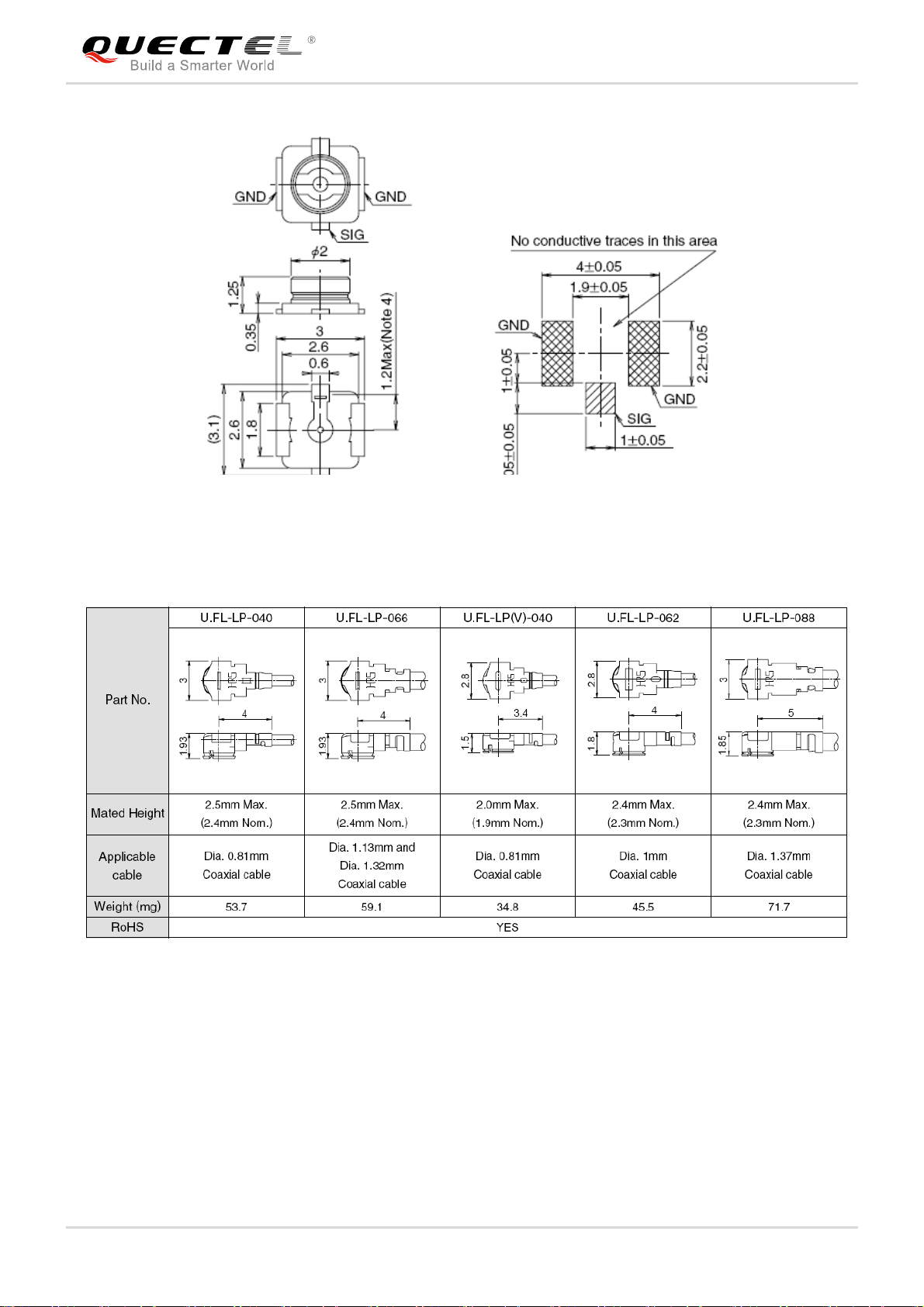
LTE Module Series
BG96 Hardware Design
Figure 28: Dimensions of the U.FL-R-SMT Connector (Unit: mm)
U.FL-LP serial connectors listed in the following figure can be used to match the U.FL-R-SMT.
Figure 29:Mechanicals of U.FL-LP Connectors
BG96_Hardware_Design 67 / 81
Page 69

d
n
e
i
s
s
S
r
o
w
d
o
r
G
d
w
s
n
B
LTE Mo
96 Hard
ule Serie
are Desig
The followi
g figure de
cribes the
pace facto
of mated c
onnector.
For mor
details,
Figure 30:
please v
pace Fact
isithttp://
r of Mate
ww.hir
Connecto
se.com.
(Unit: mm
)
BG96_Har
ware_Des
gn
68 / 81
Page 70

BG96 Hardware Design
6 Electrical, Reliability and
RadioCharacteristics
6.1. Absolute Maximum Ratings
LTE Module Series
Absolute maximum ratings for power supply and voltage on digital and analog
pins of the module are listed in the following table.
Table 31: Absolute Maximum Ratings
Parameter Min. Max. Unit
VBAT_BB
VBAT_RF
USB_VBUS
Voltage at Digital Pins
-0.5 6 V
-1.2 6 V
-0.3 5.5 V
-0.3 2.3 V
6.2. Power Supply Ratings
BG96_Hardware_Design 69 / 81
Page 71

LTE Module Series
BG96 Hardware Design
Table 32: Power Supply Ratings
Parameter Description Conditions Min. Typ. Max. Unit
The actual input voltages
VBAT VBAT_BB and VBAT_RF
must stay between the
minimum and maximum
values.
3.3 3.8 4.3 V
I
VBAT
USB_VBUS USB detection 3.0 5.0 5.25 V
Peak supply current
(during transmissionslot)
Maximum power control
level on EGSM900
1.8 2.0 A
6.3. Operation and StorageTemperatures
The operation and storagetemperatures of the modulearelisted in the following
table.
Table 33: Operation and StorageTemperatures
Parameter Min. Typ. Max. Unit
OperationTemperature Range1)
Extended Temperature Range2) -40 +85 ºC
Storage Temperature Range -40 +90 ºC
-35 +25 +75 ºC
NOTES
1. 1)Withinoperation temperature range, the module is 3GPP compliant.
2. 2)Within extended temperature range, the module remains the ability to establish and maintain a
voice, SMS, data transmission, emergency call, etc. There is no unrecoverable malfunction. There
are also no effects on radio spectrum and no harm to radio network. Only one or more parameters
like P
might reduce in their value and exceed the specified tolerances. When the temperature
out
BG96_Hardware_Design 70 / 81
Page 72

LTE Module Series
BG96 Hardware Design
returns to the normal operating temperature levels, the module will meet 3GPP specifications again.
6.4. Current Consumption
The following table shows current consumption of BG96 module.
Table 34: BG96Current Consumption
Parameter Description Conditions Typ.1) Unit
I
VBAT
Leakage
Current
PSM Power Saving Mode @Real Network 10 uA
Rock bottom
2)
Sleep
Sleep State 3)
Power off mode 8 uA
AT+CFUN=0@Sleep State
DRX=1.28s @ Instrument 1.5 mA
DRX=1.28s @ Instrument 1.96 mA
e-I-DRX=20.48s @ Instrument 1.2 mA
e-I-DRX=20.48s @ Instrument 1.1 mA
@Real 2G Network 2.0 mA
DRX=1.28s @ Instrument 15 mA
DRX=1.28s @Instrument 15 mA
0.8 mA
Idle State
LTE C at M1
data transfer
(GNSS OFF)
BG96_Hardware_Design 71 / 81
e-I-DRX=20.48s @ Instrument 15 mA
e-I-DRX=20.48s @ Instrument 15 mA
@Real 2G Network 15 mA
LTE-FDD B1 @23.31dBm
LTE-FDD B2 @23.05dBm
220 mA
208 mA
Page 73

LTE Module Series
BG96 Hardware Design
LTE-FDD B3 @23.09dBm
LTE-FDD B4 @23.19dBm
LTE-FDD B5 @23.22dBm
LTE-FDD B8 @21.83dBm
LTE-FDD B12 @21.88dBm
LTE-FDD B13 @21.96dBm
LTE-FDD B18 @23.04dBm
LTE-FDD B19 @23.13dBm
LTE-FDD B20 @23.07dBm
214 mA
214 mA
210 mA
203 mA
215 mA
197 mA
212 mA
211 mA
209 mA
LTE Cat NB1
data transfer
(GNSS OFF)
LTE-FDD B25 @23.01dBm
LTE-FDD B26 @22.81dBm
LTE-FDD B28 @22.52dBm
LTE-TDD B39 @TBD
LTE-FDD B1 @22.8dBm
LTE-FDD B2 @22.6dBm
LTE-FDD B3 @22.6dBm
LTE-FDD B4 @22.6dBm
LTE-FDD B5 @22.9dBm
211 mA
214 mA
215 mA
TBD mA
170 mA
171 mA
161 mA
161 mA
156 mA
LTE-FDD B8 @22.7dBm
LTE-FDD B12 @23dBm
LTE-FDD B13 @22.9dBm
BG96_Hardware_Design 72 / 81
170 mA
170 mA
167 mA
Page 74

LTE Module Series
BG96 Hardware Design
LTE-FDD B18 @23.1dBm
LTE-FDD B19 @22.9dBm
LTE-FDD B20 @22.7dBm
LTE-FDD B25 @23dBm
LTE-FDD B26 @22.8dBm
LTE-FDD B28 @22.5dBm
GSM850 4UL1DL @30.17dBm
GSM850 3UL2DL @32dBm
GSM850 2UL3DL @32.74dBm
159 mA
155 mA
157 mA
165 mA
162 mA
163 mA
575 mA
533 mA
402 mA
GPRS data
transfer
(GNSS OFF)
GSM850 1UL4DL @32.52dBm
EGSM900 4UL1DL @30.54dBm
EGSM900 3UL2DL @31.36dBm
EGSM9002UL3DL @32.62dBm
EGSM9001UL4DL @32.75dBm
DCS18004UL1DL @29.81dBm
DCS18003UL2DL @30.09dBm
DCS18002UL3DL @30.1dBm
DCS18001UL4DL @30.34dBm
220 mA
586 mA
556 mA
399 mA
228 mA
543 mA
426 mA
301 mA
182 mA
PCS1900 4UL1DL @29.64dBm
PCS1900 3UL2DL @29.86dBm
PCS1900 2UL3DL @29.7dBm
BG96_Hardware_Design 73 / 81
516 mA
404 mA
281 mA
Page 75

LTE Module Series
BG96 Hardware Design
EDGE data
transfer
(GNSS OFF)
PCS1900 1UL4DL @29.94dBm
GSM850 4UL1DL @26.02dBm
GSM850 3UL2DL @26.11dBm
GSM850 2UL3DL @26.57dBm
GSM850 1UL4DL @26.92dBm
EGSM900 4UL1DL @25.92dBm
EGSM900 3UL2DL @26.11dBm
EGSM9002UL3DL @26.16dBm
EGSM9001UL4DL @26.88dBm
DCS1800 4UL1DL @24.7dBm
171 mA
403 mA
312 mA
224 mA
136 mA
391 mA
301 mA
217 mA
133 mA
373 mA
NOTES
LTE Voi ce
(GNSS OFF)
DCS18003UL2DL @25.97dBm
DCS18002UL3DL @25.03dBm
DCS18001UL4DL @25.03dBm
PCS1900 4UL1DL @24.92dBm
PCS1900 3UL2DL @24.86dBm
PCS1900 2UL3DL @25.17dBm
PCS1900 1UL4DL @25.31dBm
Voice @LTE Cat M1 network
286 mA
208 mA
127 mA
375 mA
288 mA
207 mA
127 mA
108 mA
1. 1)means the average value.
2)
2.
means the operation is performed with AT+CFUN=0 and AT+QSLCK=1(DTR pin at high level).
3. 3)Sleep state with UART connected and USB disconnected. The module can enter into sleep state
BG96_Hardware_Design 74 / 81
Page 76

LTE Module Series
BG96 Hardware Design
through executing AT+QSCLK=1 command via UART interface and then controlling the module’s
DTR pin. For details, please refer to Chapter 3.4.4.
Table 35: GNSSCurrent Consumption
Description Conditions Typ. Unit
Searching
(AT+CFUN=0)
Tracking
Cold Start @Passive Antenna 41.7 mA
Lost State @Passive Antenna 42 mA
Instrument Environment 21.7 mA
Open Sky @Passive Antenna 36 mA
(AT+CFUN=0)
Open Sky @Active Antenna 35 mA
6.5. RF Output Power
The following table shows the RF output power of BG96 module.
Table 36: RF Output Power
Frequency Max. Min.
LTE-FDD
B1/B2/B3/B4/B5/B8/B12/B13/B18/B19/B20/B25/
23dBm±2dB <-39dBm
B26/B28
LTE-TDD B39 23dBm±2dB <-39dBm
GSM850/EGSM900 33dBm±2dB 5dBm±5dB
DCS1800/PCS1900 30dBm±2dB 0dBm±5dB
BG96_Hardware_Design 75 / 81
Page 77

LTE Module Series
BG96 Hardware Design
GSM850/EGSM900 (8-PSK) 27dBm±3dB 5dBm±5dB
DCS1800/PCS1900 (8-PSK) 26dBm±3dB 0dBm±5dB
6.6. RF Receiving Sensitivity
The following table shows the conducted RF receiving sensitivity of BG96
module.
Table 37: BG96 Conducted RF Receiving Sensitivity
Network Band Primary Diversity
LTE-FDD B1
LTE-FDD B2 -106.7/-100.3 -112.5/-107.5
LTE-FDD B3 -106.8/-99.3 -113/-107.5
LTE-FDD B4 -106.9/-102.3 -112.5/-107.5
LTE-FDD B5 -107.0/-100.8 -114/-107.5
LTE-FDD B8 -107.3/-99.8 -113/-107.5
Not
LTE
LTE-FDD B12 -107.7/-99.3 -113.5/-107.5
Supported
Supported
LTE-FDD B13 -106.5/-99.3 -112/-107.5
Sensitivity(dBm)
Cat M1/3GPP Cat NB11)/3GPP
-107.0/-102.7 -112.5/-107.5
LTE-FDD B18 -107.5/-102.3 -113.5/-107.5
LTE-FDD B19 -107.1/-102.3 -114/-107.5
LTE-FDD B20 -107.2/-99.8 -114/-107.5
LTE-FDD B25 -106/-100.3 -112/-107.5
LTE-FDD B26 -107.1/-100.3 -113/-107.5
BG96_Hardware_Design 76 / 81
Page 78

BG96 Hardware Design
LTE-FDD B28 -107.2/-100.8 -113/-107.5
LTE-TDD B39 TBD /-103 Not Supported
Network Band Primary Diversity
LTE Module Series
Sensitivity (dBm)
GSM/3GPP
GSM
GSM850/EGSM900
Supported
DCS1800/PCS1900 -108.5/-102
Not
Supported
Table 38: BG96-M Conducted RF Receiving Sensitivity
Network Band Primary Diversity
LTE-FDD B1
LTE-FDD B2 -106.7/-100.3
LTE-FDD B3 -106.8/-99.3
LTE-FDD B4 -106.9/-102.3
-109/-102
Sensitivity(dBm)
Cat M1/3GPP
-107.0/-102.7
LTE
LTE-FDD B5 -107.0/-100.8
LTE-FDD B8 -107.3/-99.8
LTE-FDD B12 -107.7/-99.3
Not
Supported
LTE-FDD B13 -106.5/-99.3
LTE-FDD B18 -107.5/-102.3
LTE-FDD B19 -107.1/-102.3
LTE-FDD B20 -107.2/-99.8
LTE-FDD B25 -106/-100.3
LTE-FDD B26 -107.1/-100.3
LTE-FDD B28 -107.2/-100.8
Supported
BG96_Hardware_Design 77 / 81
Page 79

LTE Module Series
BG96 Hardware Design
LTE-TDD B39 TBD /-103
NOTE
1)
LTE Cat NB1 receiving sensitivity without repetitions.
6.7. Electrostatic Discharge
The module is not protected against electrostatics discharge (ESD) in general. Consequently, it is subject
to ESD handling precautions that typically apply to ESD sensitive components. Proper ESD handling and
packaging procedures must be applied throughout the processing, handling and operation of any
application that incorporates the module.
The following table shows the electrostatic discharge characteristics of BG96 module.
Table 38: Electrostatic Discharge Characteristics
Tested Points Contact Discharge Air Discharge Unit
VBAT, GND ±10 ±15 kV
Main/GNSS Antenna
Interfaces
±10 ±15 kV
BG96_Hardware_Design 78 / 81
Page 80

LTE Module Series
BG96 Hardware Design
7 Mechanical Dimensions
This chapter describes the mechanical dimensions of the module.All dimensions are measured in mm,
and the tolerances for dimensions without tolerance values are ±0.05mm.
7.1. Mechanical Dimensions of the Module
26.50±0.15
Figure 31: Module Top and Side Dimensions
22.50±0.15
2.3±0.2
BG96_Hardware_Design 79 / 81
Page 81

LTE Module Series
BG96 Hardware Design
22.50±0.15
1.65
26.50±0.15
1.00
8.50
1.10
1.00
7.15
5.10
0.55
0.85
0.85
1.95
1.70
7.45
1.70
1.10
0.92
0.92
1.50
1.90
1.10
1.00
1.70
0.55
0.70
1.15
0.50
1.65
1.50
40x1.0
40x1.0
Figure 32: Module Bottom Dimensions (Bottom View)
62x0.7
62x1.15
BG96_Hardware_Design 80 / 81
Page 82

LTE Module Series
BG96 Hardware Design
7.2. Recommended Footprint
22.50±0.15
9.18 9.18
0.92
0.92
1.50
0.15
1.90
1.10
0.50
0.70
7.45 7.15
1.95
1.10
2.55 2.55
1.70
0.85
0.85
1.70
1.70
1.00
0.55
0.85
1.00
5.10
0.85
1.10
1.00
8.50
1.65
11.0311.03
7.657.65
5.955.95
4.254.25
26.50±0.15
9.60 9.70
4.25
5.95
62x0.7
0.55
4.25
5.95
40x1.0
1.50
40x1.0
1.65
1.15
62x1.15
Figure 33: Recommended Footprint (Top View)
NOTES
1. For easy maintenance of the module, please keep about 3mm between the module and other
components onthe host PCB.
All reserved pins must be kept open.
BG96_Hardware_Design 81 / 81
Page 83

d
c
i
n
m
g
3
T
o
u
g
f
s
t
u
G
o
g
d
w
m
e
s
n
e
B
LTE Mo
96 Hard
ule Serie
are Desig
For sten
il desig
require
ents of
7.
the mod
. Desi
le, plea
n Effec
e refer t
Drawin
docu
s of th
ent [5].
Modul
F
igure 34:
op View o
the Mod
le
Fi
ure 35: B
ttom View
of the Mod
ule
BG96_Har
ware_Des
gn
82 / 81
Page 84

LTE Module Series
BG96 Hardware Design
NOTE
These are design effect drawings of BG96 module. For more accurate pictures, please refer to the
module that you get from Quectel.
BG96_Hardware_Design 83 / 81
Page 85
LTE Module Series
BG96 Hardware Design
8 Storage, Manufacturing and
Packaging
8.1. Storage
BG96 is stored in avacuum-sealed bag. It is rated at MSL 3, and itsstorage restrictions are listed below.
1. Shelf life in the vacuum-sealed bag: 12 months at <40ºC/90%RH.
2. After the vacuum-sealed bag is opened, devices that will be subjected to reflow soldering or other
high temperature processes must be:
Mounted within 168 hours at the factory environment of ≤30ºC/60%RH.
Stored at <10%RH.
3. Devices require baking before mounting, if any circumstance below occurs.
When the ambient temperature is 23ºC±5ºCand the humidity indication card shows the humidity
is >10% before opening the vacuum-sealed bag.
Device mounting cannot be finished within 168 hours at factory conditions of ≤30ºC/60% RH.
Stored at >10% RH after the vacuum-sealed bag is opened.
4. If baking is required, devices may be baked for 8 hours at 120ºC±5ºC.
NOTE
As the plastic package cannot be subjected to high temperature, it should be removed from devices
before high temperature (120ºC) baking. If shorter baking time is desired, please refer to
IPC/JEDECJ-STD-033 for baking procedure.
BG96_Hardware_Design 84 / 81
Page 86

LTE Module Series
BG96 Hardware Design
8.2. Manufacturing and Soldering
Push the squeegee to apply the solder paste on the surface of stencil, thus making the paste fill the
stencil openings and then penetrate to the PCB. The force on the squeegee should be adjusted
properlyso as to produce a clean stencil surface on a single pass. To ensure the module soldering quality,
thethickness of stencil for the module is recommended to be 0.18mm~0.20mm. For more details, please
refer todocument [5].
It is suggested that the peak reflow temperature is 240~245ºC, and the absolute maximum reflow
temperature is 245ºC. To avoid damage to the module caused by repeated heating, it is strongly
recommended that the module should be mounted after reflow soldering for the other side of PCB has
been completed. The recommended reflow soldering thermal profile (lead-free reflow soldering) and
related parameters are shown below.
Figure 36: Recommended Reflow Soldering Thermal Profile
Table 39: Recommended Thermal Profile Parameters
Factor Recommendation
Soak Zone
BG96_Hardware_Design 85 / 81
Page 87

BG96 Hardware Design
Max slope 1 to 3°C/sec
Soak time (between A and B: 150°C and 200°C) 60 to 120 sec
LTE Module Series
Reflow Zone
Max slope 2 to 3°C/sec
Reflow time (D: over 220°C) 40 to 60 sec
Max temperature 240°C ~ 245°C
Cooling down slope 1 to 4°C/sec
Reflow Cycle
Max reflow cycle 1
8.3. Packaging
BG96 ispackaged in a vacuum-sealed bag which is ESD protected. The bag should not be opened until
the devices are ready to be soldered onto the application.
The reel is 330mm in diameter and each reel contains 250 modules.The following figures show the
packaging details, measured in mm.
BG96_Hardware_Design 86 / 81
Page 88

LTE Module Series
BG96 Hardware Design
Figure 37: Tape Dimensions
Table 40: Reel Packaging
48.5
100
44.5
+0.20
-0.00
13
Figure 38: ReelDimensions
Cover tap
e
Direction of feed
Model Name MOQ for MP MinimumPackage: 250pcs Minimum Packagex4=1000pcs
BG96 250pcs
Size: 370mm× 350mm × 56mm
N.W: 1.0kg
G.W: 1.71kg
Size: 380mm× 250mm× 365mm
N.W: 4.0kg
G.W: 7.16kg
BG96_Hardware_Design 87 / 81
Page 89

LTE Module Series
BG96 Hardware Design
9 Appendix A References
Table 41: Related Documents
SN Document Name Remark
[1] Quectel_UMTS<E_EVB_User_Guide UMTS<EEVB User Guide
[2] Quectel_BG96_AT_Commands_Manual BG96 AT Commands Manual
[3] Quectel_BG96_GNSS_AT_Commands_Manual BG96 GNSS AT Commands Manual
[4] Quectel_RF_Layout_Application_Note RF Layout Application Note
[5] Quectel_Module_Secondary_SMT_User_Guide Module Secondary SMT User Guide
Table 42: Terms and Abbreviations
Abbreviation Description
AMR Adaptive Multi-rate
bps Bits Per Second
CHAP Challenge Handshake Authentication Protocol
CS Coding Scheme
CTS Clear To Send
DFOTA Delta Firmware Upgrade Over The Air
DL Downlink
DTR Data Terminal Ready
DTX Discontinuous Transmission
e-I-DRX Extended Idle Mode Discontinuous Reception
EPC Evolved Packet Core
BG96_Hardware_Design 88 / 81
Page 90

BG96 Hardware Design
ESD Electrostatic Discharge
FDD Frequency Division Duplex
FR Full Rate
GMSK Gaussian Minimum Shift Keying
GSM Global System for Mobile Communications
HSS Home Subscriber Server
I/O Input/Output
Inorm Normal Current
LED Light Emitting Diode
LTE Module Series
LNA Low Noise Amplifier
LTE Long Term Evolution
MO Mobile Originated
MS Mobile Station (GSM engine)
MT Mobile Terminated
PAP Password Authentication Protocol
PCB Printed Circuit Board
PDU Protocol Data Unit
PPP Point-to-Point Protocol
PSM Power Saving Mode
RF Radio Frequency
RHCP Right Hand Circularly Polarized
Rx Receive
SISO Single Input Single Output
SMS Short Message Service
TDD Time Division Duplexing
BG96_Hardware_Design 89 / 81
Page 91

BG96 Hardware Design
TX Transmitting Direction
UL Uplink
UE User Equipment
URC Unsolicited Result Code
(U)SIM (Universal) Subscriber Identity Module
Vmax Maximum Voltage Value
Vnorm Normal Voltage Value
Vmin Minimum Voltage Value
VIHmax Maximum Input High Level Voltage Value
LTE Module Series
VIHmin Minimum Input High Level Voltage Value
VILmax Maximum Input Low Level Voltage Value
VILmin Minimum Input Low Level Voltage Value
VImax Absolute Maximum Input Voltage Value
VImin Absolute Minimum Input Voltage Value
VOHmax Maximum Output High Level Voltage Value
VOHmin Minimum Output High Level Voltage Value
VOLmax Maximum Output Low Level Voltage Value
VOLmin Minimum Output Low Level Voltage Value
VSWR Voltage Standing Wave Ratio
BG96_Hardware_Design 90 / 81
Page 92

LTE Module Series
BG96 Hardware Design
10 Appendix B GPRS Coding Schemes
Table 43: Description of Different Coding Schemes
Scheme
Code Rate
USF
Pre-coded USF
Radio Block excl.USF and BCS
BCS
Tail
Coded Bits
Punctured Bits
Data Rate Kb/s
CS-1 CS-2 CS-3 CS-4
1/2 2/3 3/4 1
3 3 3 3
3 6 6 12
181 268 312 428
40 16 16 16
4 4 4 -
456 588 676 456
0 132 220 -
9.05 13.4 15.6 21.4
BG96_Hardware_Design 91 / 81
Page 93

LTE Module Series
BG96 Hardware Design
11 Appendix C GPRS Multi-slot Classes
Twenty-nine classes of GPRS multi-slot modes are defined for MS in GPRS specification. Multi-slot
classes are product dependent, and determine the maximum achievable data rates in both the uplink and
downlink directions. Written as 3+1 or 2+2, the first number indicates the amount of downlink timeslots,
while the second number indicates the amount of uplink timeslots. The active slots determine the total
number of slots the GPRS device can use simultaneously for both uplink and downlink communications.
The description of different multi-slot classes is shown in the following table.
Table 44: GPRS Multi-slot Classes
Multislot Class Downlink Slots Uplink Slots Active Slots
1 1 1 2
2 2 1 3
3 2 2 3
4 3 1 4
5 2 2 4
6 3 2 4
7 3 3 4
8 4 1 5
9 3 2 5
10 4 2 5
11 4 3 5
12 4 4 5
13 3 3 NA
14 4 4 NA
BG96_Hardware_Design 92 / 81
Page 94

LTE Module Series
BG96 Hardware Design
15 5 5 NA
16 6 6 NA
17 7 7 NA
18 8 8 NA
19 6 2 NA
20 6 3 NA
21 6 4 NA
22 6 4 NA
23 6 6 NA
24 8 2 NA
25 8 3 NA
26 8 4 NA
27 8 4 NA
28 8 6 NA
29 8 8 NA
30 5 1 6
31 5 2 6
32 5 3 6
33 5 4 6
BG96_Hardware_Design 93 / 81
Page 95

LTE Module Series
BG96 Hardware Design
12 Appendix D EDGE Modulationand
Coding Schemes
Table 45: EDGE Modulation and Coding Schemes
Coding
Schemes
CS-1: GMSK / 9.05kbps 18.1kbps 36.2kbps
CS-2: GMSK / 13.4kbps 26.8kbps 53.6kbps
CS-3: GMSK / 15.6kbps 31.2kbps 62.4kbps
CS-4: GMSK / 21.4kbps 42.8kbps 85.6kbps
MCS-1 GMSK C 8.80kbps 17.60kbps 35.20kbps
MCS-2 GMSK B 11.2kbps 22.4kbps 44.8kbps
MCS-3 GMSK A 14.8kbps 29.6kbps 59.2kbps
MCS-4 GMSK C 17.6kbps 35.2kbps 70.4kbps
MCS-5 8-PSK B 22.4kbps 44.8kbps 89.6kbps
MCS-6 8-PSK A 29.6kbps 59.2kbps 118.4kbps
Modulation Coding Famil y 1 Timeslot 2 Timeslot 4 Timeslot
MCS-7 8-PSK B 44.8kbps 89.6kbps 179.2kbps
MCS-8 8-PSK A 54.4kbps 108.8kbps 217.6kbps
MCS-9 8-PSK A 59.2kbps 118.4kbps 236.8kbps
BG96_Hardware_Design 94 / 81
 Loading...