

Page 1
Q-TECH
0.1
0.052
(1.3)
(2.54)
0.047
(1.2)
0.039
(1.0)
1
4 3
2
50.0 D/C
Q325L
0.13±.004
(3.2±0.1)
0.2±.004
(5.0±0.1)
0.047
(1.2)
12
34
max.
0.087
0.063
0.055
(1.4)
(2.2)
0.1
(2.54)
(1.6)
COR PORATI ON
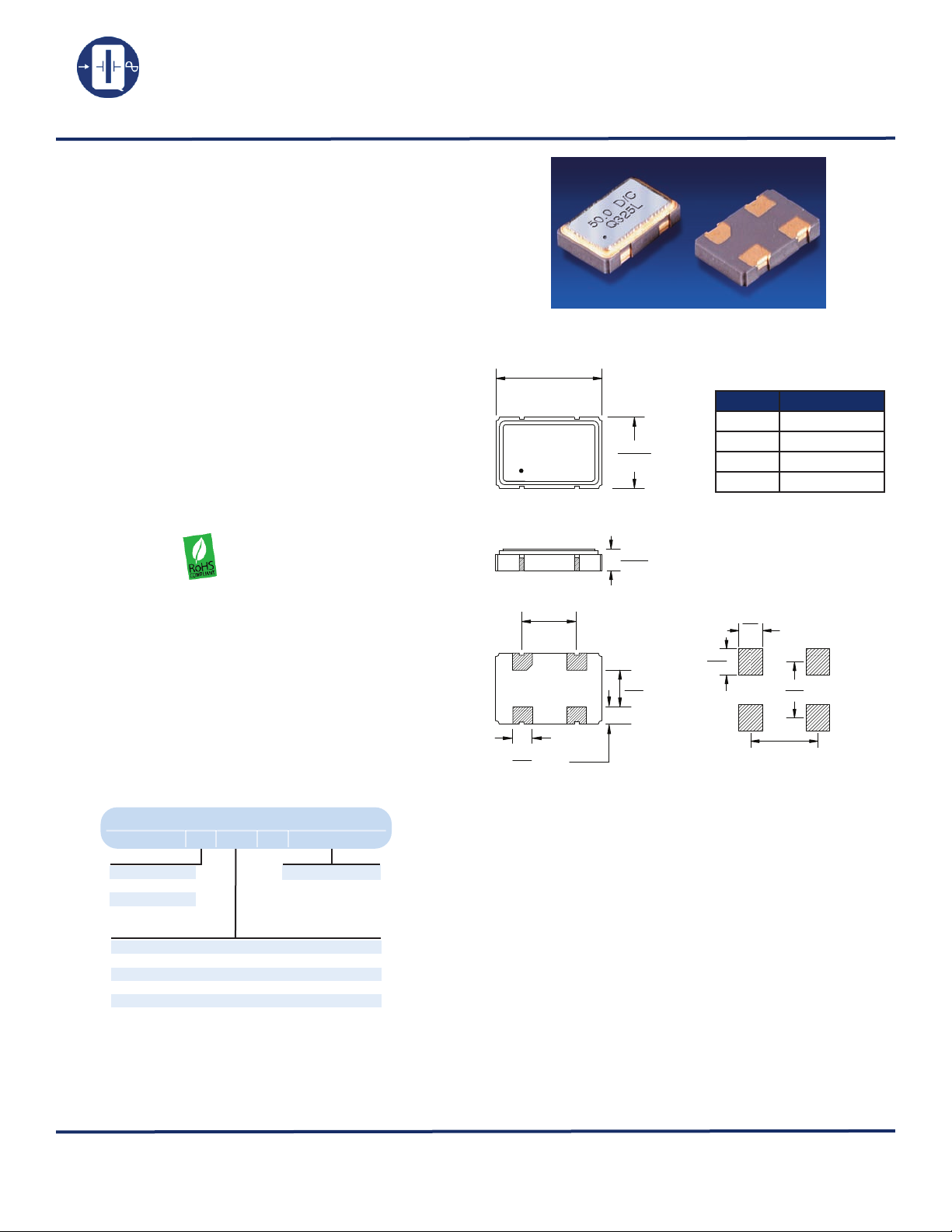
LOW PROFILE 5 x 3.2mm MINIATURE SMD CRYSTAL OSCILLATORS
Description
Q-Tech’s surface-mount QCC325 oscillators consist of an IC
5Vdc, 3.3Vdc, 2.5Vdc, 1.8Vdc clock square wave generator
and a miniature strip AT quartz crystal built in a low profile
ceramic package with gold plated contact pads.
Features
• ECCN: EAR99
• Broad frequency range from 1MHz to 220.000MHz
• Small footprint
• LVHCMOS, HCMOS, and TTL compatible
• 5.0Vdc, 3.3Vdc, 2.5Vdc, 1.8Vdc supply
• Able to meet 36000G shock per ITOP 1-2-601
• Operating temperature -40ºC to +85ºC
• Tri-State Output Standard
• Hermetically sealed ceramic package
• Fundamental and 3rd Overtone designs
• Full or partial military screening tests available
• Tape and reel packaging
• RoHS compliant
QCC325 SERIES
1.8 to 5.0Vdc - 1MHz to 220.000MHz
Package Specifications and Outline
Pin No.
1
2
3
4
Function
TRISTATE
GND/CASE
OUTPUT
VDD
Applications
• Designed to meet today’s requirements for low voltage
applications
• Gun launched munitions and systems
• Smart munitions
• Instrumentation
• Navigation
• Avionics
• Microprocessor clock
Ordering Information
For Non-Standard requirements, contact Q-Tech Corporation at Sales@Q-Tech.com
Other Options Available For An Additional Charge
• Hot Solder Dip Sn60 per MIL-PRF 55310
QCC325 (Revision F, August 2010) (ECO# 9911)
An external bypass capacitor 0.01µF is
Sample part number
QCC325N5-50. 0 0 0 M H z
QCC325 N5 -50.000MHz
Blank= 5.0Vdc
L= 3.3Vdc
N= 2.5Vdc
R= 1.8Vdc
N/A = ±
5 = ± 25ppm
12 = ±
50ppm
100ppm
14 = ± 20ppm at -20ºC to +70ºC
15
= ± 25ppm
Frequency stability vs. temperature codes may not be available in all frequencies.
Output frequency
at
-40ºC to
at
-20ºC to +70ºC
at
-40ºC to
at
-40ºC to +85ºC
+85ºC
+85ºC
Dimensions are in inches (mm)
Marking Information:
Line 1: XX.XX + D/C
(Frequency in MHz + Date code Month Year)
Line 2: Dot + P/N + Stability code
(Dot + 6 characters max.)
Date Code Format:
A - L: Month Jan-Dec
0 : 2010
1 : 2011
Package Information
• Package material: AL2O
3
required between Vdd and GND
• Termination pads (4x), Electro nickel plating 1.27µm ~ 8.89µm typ.,
with gold 0.3µm ~ 1.0µm flash plate
Specifications subject to change without prior notice.
Q-TECH Corporation - 10150 W. Jefferson Boulevard, Culver City 90232 - Tel: 310-836-7900 - Fax: 310-836-2157 - www.q-t ech.c om
• Weight: 0.06g typ., 2.0g max.
1
Page 2
Q-TECH
COR PORATI ON
Electrical Characteristics
QCC325 SERIES
LOW PROFILE 5 x 3.2mm MINIATURE SMD CRYSTAL OSCILLATORS
1.8 to 5.0Vdc - 1MHz to 220.000MHz
Parameters
Output frequency range (Fo)
Supply voltage (Vdd)
Maximum Applied Voltage (Vdd max.)
Frequency stability (∆F/∆T)
Operating temperature (Topr) -40ºC to +85ºC
Storage temperature (Tsto) -55ºC to + 125ºC
Operating supply current
(No Load)
Symmetry
(50% of ouput waveform )
Rise and Fall times
Output Load
Start-up time (Tstup) 10ms max.
35 mA max. - 1MHz ~ < 32MHz
70 mA max. - 32MHz ~ < 70MHz
90 mA max. - 70MHz ~ 106.250MHz
10ns max. - 1MHz ~ < 20MHz
7ns max. - 20MHz ~ 106.250MHz
15pF max. (50MHz ~ 106.250MHz)
QCC325 QCC325L QCC325N QCC325R
1MHz — 106.250MHz 1MHz — 220.000MHz 1MHz — 220.000MHz 1MHz — 165.000MHz
5.0Vdc ± 10% 3.3Vdc ± 10%
-0.5 to +7.0Vdc
± 50ppm max.
(between 10% to 90%)
30pF max. 1MHz ~ < 50MHz
20 mA max. - 1MHz ~ < 32MHz
45 mA max. - 32MHz ~ < 70MHz
100 mA max. - 70MHz ~ 220.000MHz
8ns max. - 1MHz ~ < 20MHz
5ns max. - 20MHz ~ 220.000MHz
(between 10% to 90%)
15pF max. 15pF max.
22 mA max. - 30MHz ~ < 60MHz
70 mA max. - 60MHz ~ 220.000MHz
45/55%
2.5Vdc ± 10%
-0.5 to +5.0Vdc
8 mA max. - 1MHz ~ < 30MHz
(between 20% to 80%)
1.8Vdc ± 10%
7 mA max. - 1MHz ~ < 30MHz
18 mA max. - 30MHz ~ < 70MHz
61 mA max - 70MHz ~ 165MHz
6ns max.
Output voltage (Voh/Vol)
Output Current (Ioh/Iol)
Enable/Disable function Pin 1
Aging ± 5ppm/year max.
Q-TECH Corporation - 10150 W. Jefferson Boulevard, Culver City 90232 - Tel: 310-836-7900 - Fax: 310-836-2157 - www.q-te ch.com
QCC325 (Revision F, August 2010) (ECO# 9911)
± 16mA max.
VIH ≥ 2.2V Active
VIL ≤ 0.8V High Z
± 8mA max.
VIH ≥ 2.2V Active (< 30MHz)
VIH ≥ 0.7Vdd Active (≥ 30MHz)
VIL ≤ 0.8V High Z (< 30MHz)
VIL ≤ 0.3Vdd High Z (≥ 30MHz)
0.9Vdd min. / 0.1Vdd max.
± 6mA max.
VIH ≥ 0.7Vdd Active
VIL ≤ 0.3Vdd High Z
2
Page 3

Q-TECH
Vdd
GND
0.1xVdd
0.9xVdd
VOH
VOL
Tr Tf
TH
T
0.5xVdd
SYMMETRY = x 100%
TH
T
0 20 40 60 80 100 120 140 160
180
200 220 240 260
280
300 320 340 360 380 400 420 Time (s)
25
50
75
100
125
150
175
200
225
250
TEMP(*C)
0
60s min.
120s max.
60s min.
120s max.
225º min.
240º max.
60s min.
150s max.
240º
Ramp down (6ºC/s Max)
Ramp up (3ºC/s Max)
TYPICAL REFLOW PROFILE FOR Sn-Pb ASSEMBLY
FEEDING (PULL) DIRECTION
ø13.0±0.5
2.5
1.4±0.1
5º MAX
ø1.5
2.0
1.75±0.1
0.3±.005
ø1.5
2.0±0.1
5.5±0.1
3.5±0.1
4.0±0.1
ø80±1
ø178±1
17.5
12.0±0.3
8±0.1
5.4
±0.1
120º
-
-
Output
Ground
4
3
2
0.1µF
15pF
1
Tristate Function
Power
supply
10k
mA
Vdc
+
+
+
(*)
or
0.01µF
QCC325
(*) CL includes probe and jig capacitance
Typical test circuit for CMOS logic
FREQUENCY VS. TEMPERATURE QCC325L15 20MHz
-6
-5
-4
-3
-2
-1
0
1
2
3
4
-40 -25 -10 5 15 25 40 55 70 85
Temp (°C)
pp m
COR PORATI ON
QCC325 SERIES
LOW PROFILE 5 x 3.2mm MINIATURE SMD CRYSTAL OSCILLATORS
1.8 to 5.0Vdc - 1MHz to 220.000MHz
Output Waveform (Typical)
Frequency vs. Temperature Curve
Reflow Profile
Test Circuit
The Tristate function on pin 1 has a built-in pull-up resistor so it can be left
floating or tied to Vdd without deteriorating the electrical performance.
Embossed Tape and Reel Information
Environmental Test Test Conditions
Environmental and Mechanical Specifications
Temperature cycling MIL-STD-883, Method 1010, Cond. B
Constant acceleration MIL-STD-883, Method 2001, Cond. A, Y1
Seal: Fine and Gross Leak MIL-STD-883, Method 1014, Cond. A and C
Vibration sinusoidal MIL-STD-202, Method 204, Cond. D
Shock, non operating MIL-STD-202, Method 213, Cond. I
Resistance to solder heat MIL-STD-202, Method 210, Cond. B
Resistance to solvents MIL-STD-202, Method 215
Solderability MIL-STD-202, Method 208
ESD Classification MIL-STD-883, Method 3015, Class 1 HBM 0 to 1,999V
Moisture Sensitivity Level J-STD-020, MSL=1
Q-TECH Corporation - 10150 W. Jefferson Boulevard, Culver City 90232 - Tel: 310-836-7900 - Fax: 310-836-2157 - www.q-t ech.c om
QCC325 (Revision F, August 2010) (ECO# 9911)
Dimensions are in mm. Tape is compliant to EIA-481-A.
Reel size (Diameter in mm)
178
Qty per reel (pcs)
1,000
3
Page 4

QCC325 SERIES
Q-TECH
COR PORATI ON
Phase Noise and Phase Jitter Integration
Phase noise is measured in the frequency domain, and is expressed as a ratio of signal power to noise power measured in a 1Hz
bandwidth at an offset frequency from the carrier, e.g. 10Hz, 100Hz, 1kHz, 10kHz, 100kHz, etc. Phase noise measurement is made
with an Agilent E5052A Signal Source Analyzer (SSA) with built-in outstanding low-noise DC power supply source. The DC source
is floated from the ground and isolated from external noise to ensure accuracy and repeatability.
In order to determine the total noise power over a certain frequency range (bandwidth), the time domain must be analyzed in the
frequency domain, and then reconstructed in the time domain into an rms value with the unwanted frequencies excluded. This may be
done by converting L(f) back to Sφ(f) over the bandwidth of interest, integrating and performing some calculations.
LOW PROFILE 5 x 3.2mm MINIATURE SMD CRYSTAL OSCILLATORS
1.8 to 5.0Vdc - 1MHz to 220.000MHz
Symbol
∫L(f)
Sφ (f)=(180/Π)x√2 ∫L(f)df
RMS jitter = Sφ (f)/(fosc.360°) Jitter(in seconds) due to phase noise. Note Sφ (f) in degrees.
Integrated single side band phase noise (dBc)
Spectral density of phase modulation, also known as RMS phase error (in degrees)
Definition
The value of RMS jitter over the bandwidth of interest, e.g. 10kHz to 20MHz, 10Hz to 20MHz, represents 1 standard deviation of
phase jitter contributed by the noise in that defined bandwidth.
Figure below shows a typical Phase Noise/Phase jitter of a QCC325, 3.3Vdc, 25MHz clock at offset frequencies 1Hz to 1MHz, and
phase jitter integrated over the bandwidth of 12kHz to 1MHz.
Q-TECH Corporation - 10150 W. Jefferson Boulevard, Culver City 90232 - Tel: 310-836-7900 - Fax: 310-836-2157 - www.q-t ech.c om
QCC325 (Revision F, August 2010) (ECO# 9911)
44
 Loading...