

Page 1
Q-TECH
COR PORATI ON
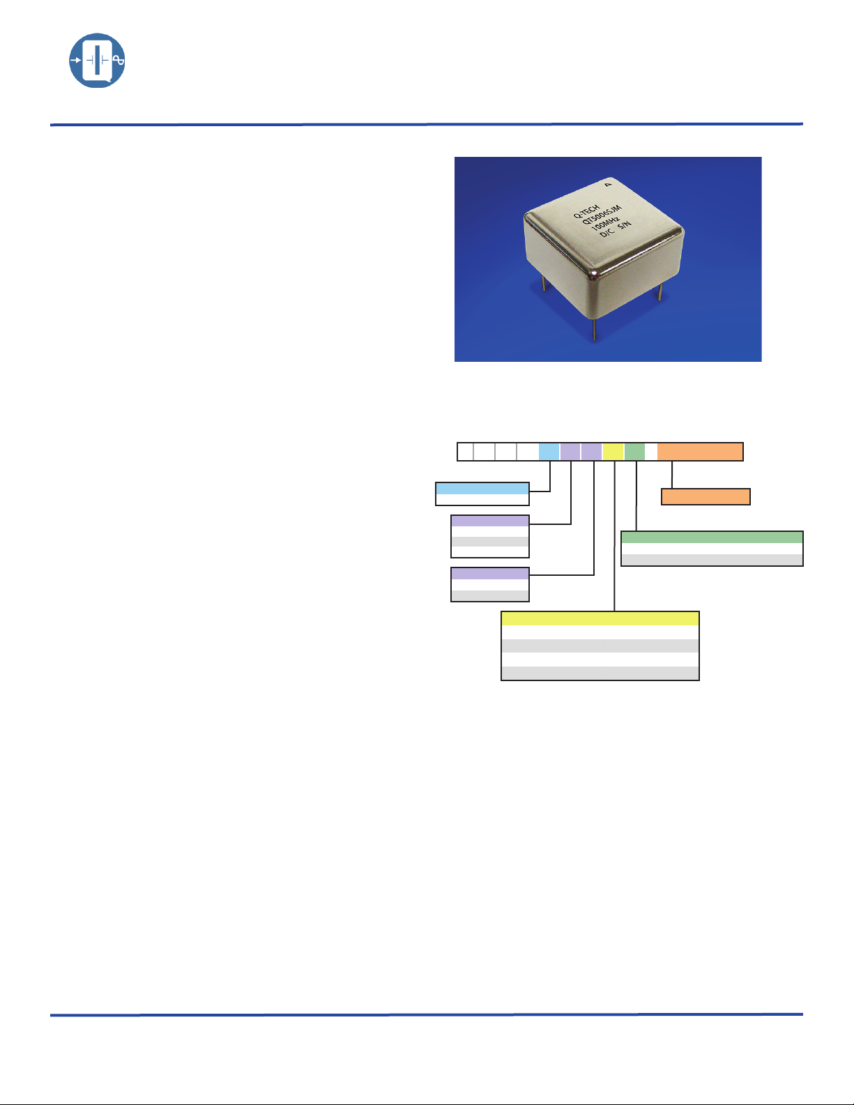
ONE INCH SQUARE LOW PHASE NOISE OCXO
Description
Q-Tech’s High Stability OCXO is a high reliability signal
generator that provides an HCMOS or Sine Wave output. The
OCXO is available in a Through hole package.
A flexible design allows Q-Tech Corporation to offer a variety
of choices of output standard, power and load. Based on this
flexibility, Q-Tech welcomes specifications with parameters
other than standard.
Low G-Sensitivity SC-Cut Crystal utilized in the design
guarantees 1PPB/G or better. The reliable construction of this
design qualifies it for stringent environmental applications.
Features
3.3 to 12Vdc - 1MHz to 125MHz
Ordering Information
(Sample part number)
QT5006SJM-10 0 . 0 0 0 MHz
Q T 5 0 0 6 S J M- 100.000MHz
• Made in the USA
• ECCN: EAR99
• DFARS 252-225-7014 Compliant:
Electronic Component Exemption
• USML Registration # M17677
• Supply voltages 3.3Vdc, 5Vdc and 12Vdc
• Wide temperature range (-40ºC to +85ºC)
• SC-Cut crystal
• Low phase noise and jitter
• Choice of output power and load
• Hermetically sealed packages
• Custom design available tailored to meet customer’s needs
• Q-Tech does not use pure lead or pure tin in its products
Applications
• Designed to meet today’s requirements for communication
systems.
• Wide military clock applications
• Control and measurement
• Signal processing
Package Type:
0 Through Hole
Supply Voltage:
3 +3.3V
5 +5.0V
6 +12.0V
Logic:
C HCMOS
S Sine Wave
Frequency vs. Temperature Code
G ± 100PPB at -20ºC to +70ºC
H ± 10PPB at -20ºC to +70ºC
J ± 200PPB at -40ºC to +85ºC
D ± 20PPB at -40ºC to +85ºC
For Non-Standard requirements, contact Q-Tech Corporation at
Sales@Q-Tech.com
Output Frequency
Blank No Screening
Screening Option:
M Per MIL-PRF-55310, Level B
Packaging Options
• Standard packaging in black foam
Other Options Available For An Additional Charge
• P. I. N. D. test (MIL-STD 883, Method 2020)
• Phase Noise test (Static and under vibration)
• Jitter test
Specifications subject to change without prior notice.
Q-TECH Corporation - 10150 W. Jefferson Boulevard, Culver City 90232 - Tel: 310-836-7900 - Fax: 310-836-2157 - www.q-te ch.co m
QPDS-0005 (Revision A, April 2013 )(ECO # 10836)
1 of 6
Page 2

Q-TECH
COR PORATI ON
ONE INCH SQUARE LOW PHASE NOISE OCXO
3.3 to 12Vdc - 1MHz to 125MHz
Electrical Characteristics
Parameters Conditions Requirements
Output Frequency Range
Supply Voltage ±5.0% 3.3V, 5V and 12V
Initial Tolerance @+25°C ±50 PPB
Temperature Range See Option Codes
Frequency Stability vs. Temperature See Option Codes
Frequency Stability vs. Voltage Variation Over temperature range ±20 PPB
Frequency Stability vs. Load Variation ±5.0% Load Variation ±20 PPB
Warm-up Power @-40°C 4.5W (for codes D and J)
Steady State Power @+25°C 1.5W (for codes D and J)
Warm-up Time @+25°C to ±100PPB (shours ref.) 5min
Output Waveform
Output Power +3.0±1.0 dBm
Output Power Stability Over temperature range ±1.0 dBm
Duty Cycle
Output Load
Harmonics
Spurious
Aging
Phase Noise for 100MHz OCXO (typ.)
Over temperature range 50%±5.0%
Over temperature range -35dBc
Over temperature range -90dBc
Per day 1PPB
15 years 1.5PPM
10Hz -90dBc/Hz
100Hz -120dBc/Hz
1kHz -150dBc/Hz
10kHz -160dBc/Hz
100kHz -162dBc/Hz
1MHz — 125MHz
Sine Wave HCMOS
50Ω 10kΩ//15pF
Other Design and Test Options
• Supply voltage +3.3Vdc to +12Vdc
• Phase Noise and Jitter built to specification including static
and vibration.
• QCI tests
• Tight frequency stability versus temperature, supply voltage,
and load variations
• Low g-sensitivity and low phase noise
• Low spurious (see note 3)
• Low frequency aging, Allan Variance
• High-shock resistant
Q-TECH Corporation - 10150 W. Jefferson Boulevard, Culver City 90232 - Tel: 310-836-7900 - Fax: 310-836-2157 - www.q-te ch.co m
QPDS-0005 (Revision A, April 2013 )(ECO # 10836)
Notes:
1. The output level is determined by the supply voltage, load,
and package size.
2. Typical amplitude stability over temperature is ±10% or less.
3. Typical spurious level is better than -100dBc over the
spectrum of 100kHz to 1GHz.
4. Guaranteed by design, can be tested by customer request.
2 of 6
Page 3

Q-TECH
COR PORATI ON
Package Outline and Pin Connections
Dimensions are in inches (mm)
ONE INCH SQUARE LOW PHASE NOISE OCXO
3.3 to 12Vdc - 1MHz to 125MHz
Pin No.
1
2
3
4
5
Designation
OUTPUT
GND/CASE
VOLTAGE CONTROL
NC
SUPPLY VOLTAGE
Package Information
Package Material: COLD ROLLED Steel
Bright Nickel Plated 500µ inches
NC (No Connection)
Q-TECH Corporation - 10150 W. Jefferson Boulevard, Culver City 90232 - Tel: 310-836-7900 - Fax: 310-836-2157 - www.q-te ch.co m
QPDS-0005 (Revision A, April 2013 )(ECO # 10836)
3 of 6
Page 4

Q-TECH
COR PORATI ON
ONE INCH SQUARE LOW PHASE NOISE OCXO
3.3 to 12Vdc - 1MHz to 125MHz
Sine Wave Output Waveform into 50Ω load Test Circuit
HCMOS Load
Typical output of QT5006SJ-100.000MHz
Sine Wave Load
Typical Amplitude for Sine Wave Output Sine Wave Output Harmonic Distortion
Q-TECH Corporation - 10150 W. Jefferson Boulevard, Culver City 90232 - Tel: 310-836-7900 - Fax: 310-836-2157 - www.q-te ch.co m
QPDS-0005 (Revision A, April 2013 )(ECO # 10836)
4 of 6
Page 5

Q-TECH
COR PORATI ON
Frequency vs. Temperature Curve
ONE INCH SQUARE LOW PHASE NOISE OCXO
3.3 to 12Vdc - 1MHz to 125MHz
Typical Stability of QT5006SJ-100.000MHz
Environmental Specifications
Q-Tech Standard Screening similar to (MIL-PRF-55310) is available. Q-Tech can also customize screening and test procedures to meet
your specific requirements. The packages are designed and processed to exceed the following test conditions:
Environmental Test Test Conditions
Temperature cycling MIL STD 883, Method 1010, Cond. B
Constant acceleration MIL STD 883, Method 2001, Cond. A, Y1
Seal Fine Leak MIL STD 883, Method 1014, Cond. A
Burn in 160 hours, 125°C with load
Aging 30 days, 70°C
Vibration sinusoidal MIL STD 202, Method 204, Cond. D
Shock, non operating MIL STD 202, Method 213, Cond. I
Thermal shock, non operating MIL STD 202, Method 107, Cond. B
Ambient pressure, non operating MIL STD 202, 105, Cond. C, 5 minutes dwell time minimum
Resistance to solder heat MIL STD 202, Method 210, Cond. C
Moisture resistance MIL STD 202, Method 106
Terminal strength MIL STD 202, Method 211, Cond. C
Resistance to solvents MIL STD 202, Method 215
Solderability MIL STD 202, Method 208
ESD Classification MIL STD 883, Method 3015, Class 1HBM 0 to 1,999V
Moisture Sensitivity Level J STD 020, MSL 1
Please contact Q-Tech for higher shock requirements
Q-TECH Corporation - 10150 W. Jefferson Boulevard, Culver City 90232 - Tel: 310-836-7900 - Fax: 310-836-2157 - www.q-te ch.co m
QPDS-0005 (Revision A, April 2013 )(ECO # 10836)
5 of 6
Page 6
Q-TECH
COR PORATI ON
ONE INCH SQUARE LOW PHASE NOISE OCXO
3.3 to 12Vdc - 1MHz to 125MHz
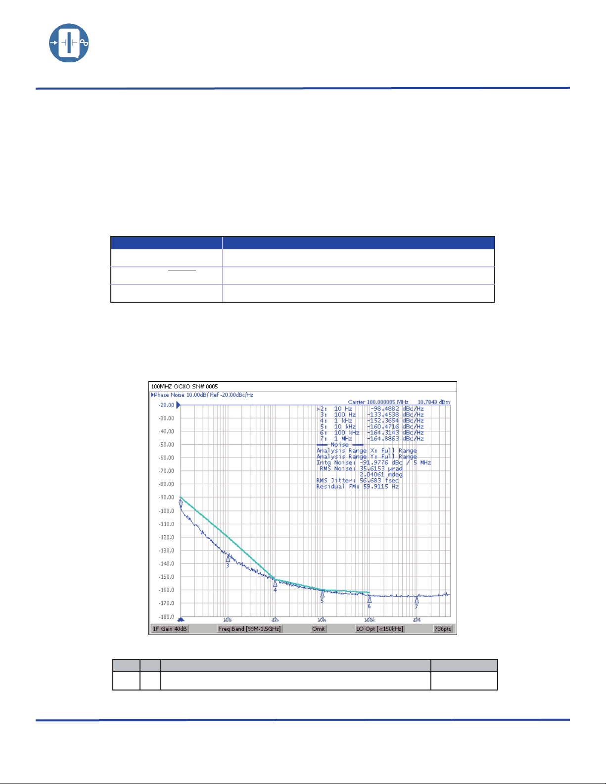
Phase Noise and Phase Jitter Integration
Phase noise is measured in the frequency domain, and is expressed as a ratio of signal power to noise power measured in a 1Hz bandwidth
at an offset frequency from the carrier, e.g. 10Hz, 100Hz, 1kHz, 10kHz, 100kHz, etc. Phase noise measurement is made with an Agilent
E5052A Signal Source Analyzer (SSA) with built-in outstanding low-noise DC power supply source. The DC source is floated from the
ground and isolated from external noise to ensure accuracy and repeatability.
In order to determine the total noise power over a certain frequency range (bandwidth), the time domain must be analyzed in the frequency
domain, and then reconstructed in the time domain into an RMS value with the unwanted frequencies excluded. This may be done by
converting L(f) back to Sφ(f) over the bandwidth of interest, integrating and performing some calculations.
Symbol
∫L(f)
Sφ (f) (180/Π)x√2 ∫L(f)df
RMS jitter Sφ (f)/(fosc.360°) Jitter(in seconds) due to phase noise. Note Sφ (f) in degrees.
Integrated single side band phase noise (dBc)
Spectral density of phase modulation, also known as RMS phase error (in degrees)
Definition
The value of RMS jitter over the bandwidth of interest, e.g. 10kHz to 20MHz, 10Hz to 20MHz, represents 1 standard deviation of
phase jitter contributed by the noise in that defined bandwidth.
Figure below shows a typical phase noise/phase jitter of a QT5006S, 12V, 100.000MHz OCXO at offset frequencies 10Hz to 5MHz.
QT5006SJ-100.000MHz
ECO REV REVISION SUMMARY Page
10836
Q-TECH Corporation - 10150 W. Jefferson Boulevard, Culver City 90232 - Tel: 310-836-7900 - Fax: 310-836-2157 - www.q-te ch.co m
QPDS-0005 (Revision A, April 2013 )(ECO # 10836)
A Fixed typo under “Other Design and Test Options” (from see note 5 to 3) 2
6 of 6
 Loading...