

Page 1
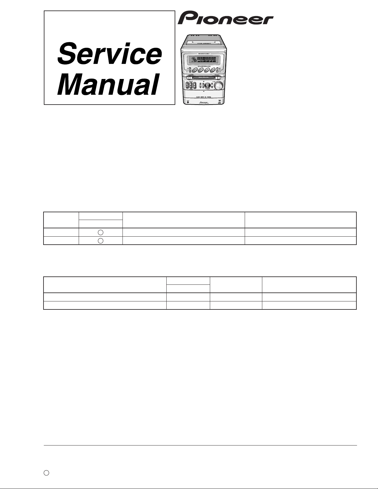
XR-C2MD
MD/CD COMPONENT SYSTEM
X-MDX707
XR-C2MD
THIS MANUAL IS APPLICABLE TO THE FOLLOWING MODEL(S) AND TYPE(S).
Type
LBWXJ AC110V
NLWXJ/HK AC220V
¶ X-MDX707 is combination of the following components.
¶ For speaker system S-C2-LR, refer to the service manual RRV2156.
STEREO MD/CD CASSETTE DECK RECEIVER XR-C2MD RRV2165 This manual.
SPEAKER SYSTEM S-C2-LR RRV2156
Model
XR-C2MD
Component
Power Requirement Remarks
Model
X-MDX707
Service manual Remarks
ORDER NO.
RRV2165
CONTENTS
1. SAFETY INFORMATION
2. EXPLODED VIEWS AND PARTS LIST
3. BLOCK DIAGRAM AND SCHEMATIC DIAGRAM
4. PCB CONNECTION DIAGRAM
5. PCB PARTS LIST
6. ADJUSTMENT
PIONEER CORPORATION 4-1, Meguro 1-chome, Meguro-ku, Tokyo 153-8654, Japan
PIONEER ELECTRONICS SERVICE, INC. P.O. Box 1760, Long Beach, CA 90801-1760, U.S.A.
PIONEER ELECTRONIC (EUROPE) N.V. Haven 1087, Keetberglaan 1, 9120 Melsele, Belgium
PIONEER ELECTRONICS ASIACENTRE PTE. LTD. 253 Alexandra Road, #04-01, Singapore 159936
c
PIONEER CORPORATION 1999
...............................................
....................................................
......................................
...............
...
.........................
18
40
54
60
2
3
7. GENERAL INFORMATION
7.1 DIAGNOSIS
7.1.1 TROUBLESHOOTING
7.1.2 DISASSEMBLY/ASSEMBLY
7.2 PARTS
7.2.1 IC
7.2.2 DISPLAY
8. PANEL FACILITIES AND SPECIFICATIONS
..................................................
..........................................................
............................................................
.................................................
................................
...........................
..................
T – ZZK AUG. 1999 Printed in Japan
.......
68
68
68
78
86
86
90
93
Page 2
X-MDX707, XR-C2MD
1. SAFETY INFORMATION
This service manual is intended for qualified service technicians ; it is not meant for the casual do-ityourselfer. Qualified technicians have the necessary test equipment and tools, and have been trained
to properly and safely repair complex products such as those covered by this manual.
Improperly performed repairs can adversely affect the safety and reliability of the product and may
void the warranty. If you are not qualified to perform the repair of this product properly and safely, you
should not risk trying to do so and refer the repair to a qualified service technician.
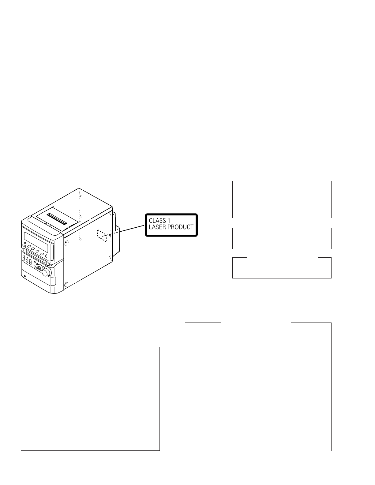
LABEL CHECK
Additional Laser Caution
of CD PLAYER
1.Laser Interlock Mechanism
The position of the switch for detecting loading state is
detected by the system microprocessor, and the design
prevents laser diode oscillation when the switch is
pressed physically.
Thus, the interlock will no longer function if the switch is
released physically and deliberatery.
Laser diode oscillation will continue, if pin 33 of
CXA1782BQ (IC803) on the CD UNIT is connected to
GND, or else the terminals of Q802 are shorted to each
other (fault condition).
2.When the cover is opened, close viewing of the
objective lens with the naked eye will cause exposure
to a Class 1 laser beam.
THIS PIONEER APPARATUS CONTAINS
IMPORTANT
LASER OF CLASS 1.
SERVICING OPERATION OF THE APPARATUS
SHOULD BE DONE BY A SPECIALLY
INSTRUCTED PERSON.
LASER DIODE CHARACTERISTICS
OF CD PLAYER
MAXIMUM OUTPUT POWER: 5 mW
WAVELENGTH: 760 - 800 nm
LASER DIODE CHARACTERISTICS
OF MD RECORDER
MAXIMUM OUTPUT POWER: 40 mW
WAVELENGTH: 775 - 800 nm
Additional Laser Caution
of MD RECORDER
Control method of the current through a laser diode.
The resistor R166 on the MD MOUNT ASSY (For MD mechanism
assembly) are for the limiting of current through a laser diode.
Control method of the laser output power
The laser pick-up assembly provide the photo-diodes and APC
(Auto Power Control) circuit.
The photo-diode detect output of the laser diode then IC201 control
the APC circuit according to the signal voltage of the photo-diode via
IC101.
Laser Interlock Switch
The loading position detect switch is set to “ LOAD ON ” position,
IC201 get the “ LOAD ” signal, and hand the laser “ LDON ” signal to
APC (Auto Power Control) circuit of the Laser pick-up assembly.
Then a laser diode can be lighted when the “ LOAD ”signal is “
LOAD ON ” position.
2
Page 3
S-C2-LR
5
XR-C2MD
3
4
10
11
13
16
2
1
12
14
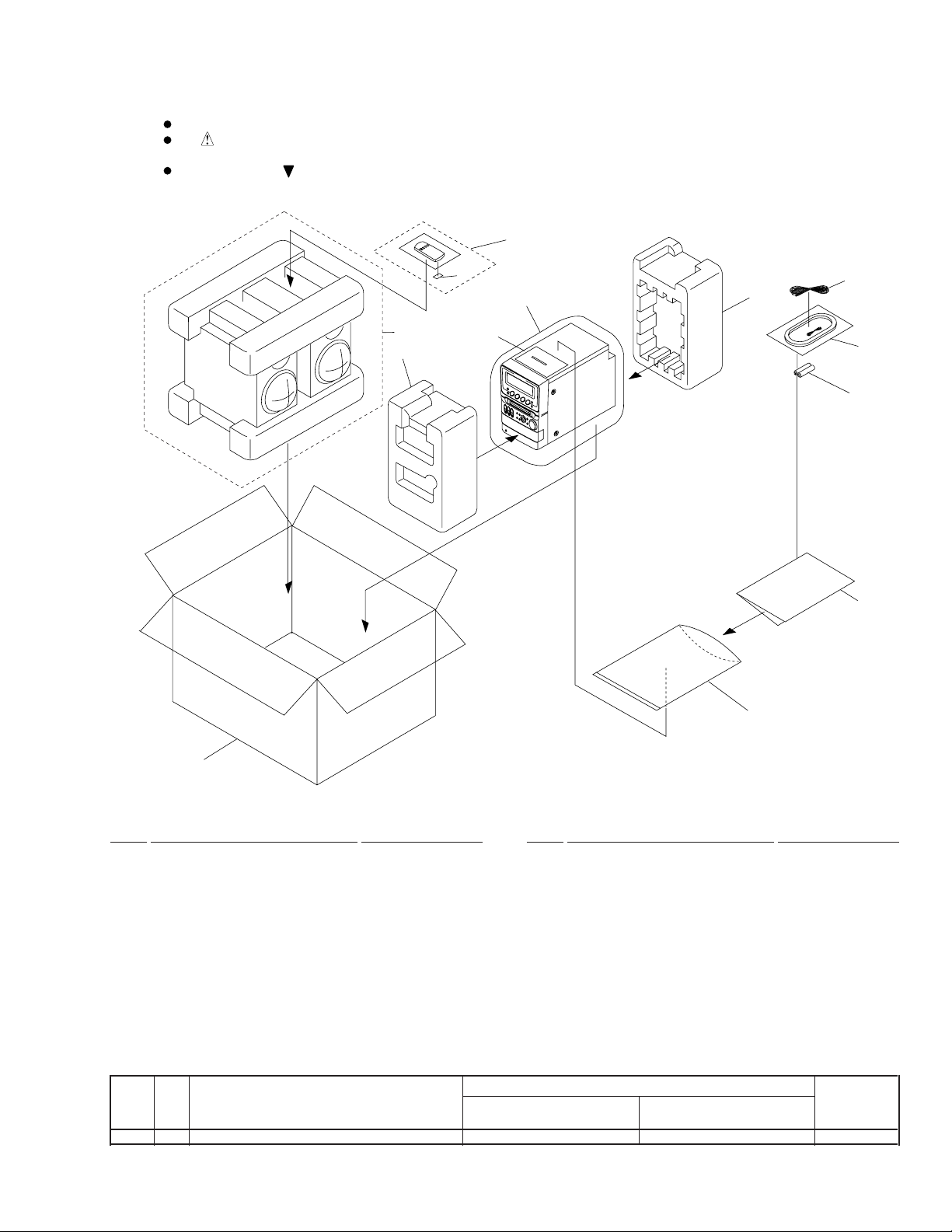
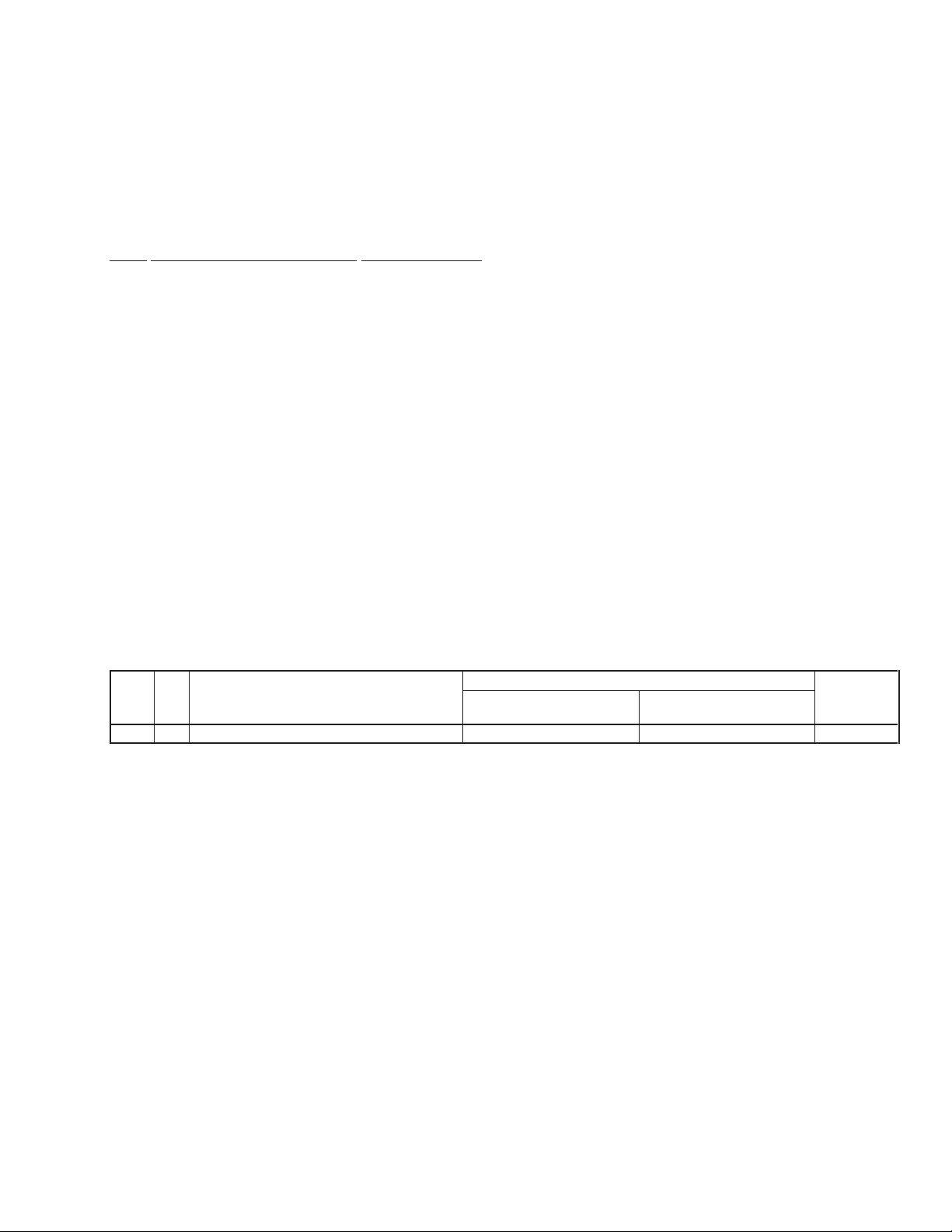
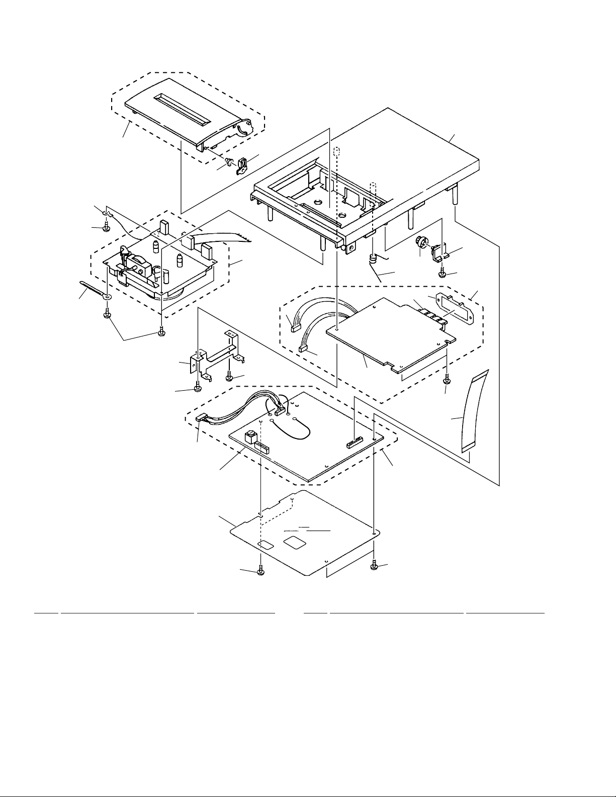
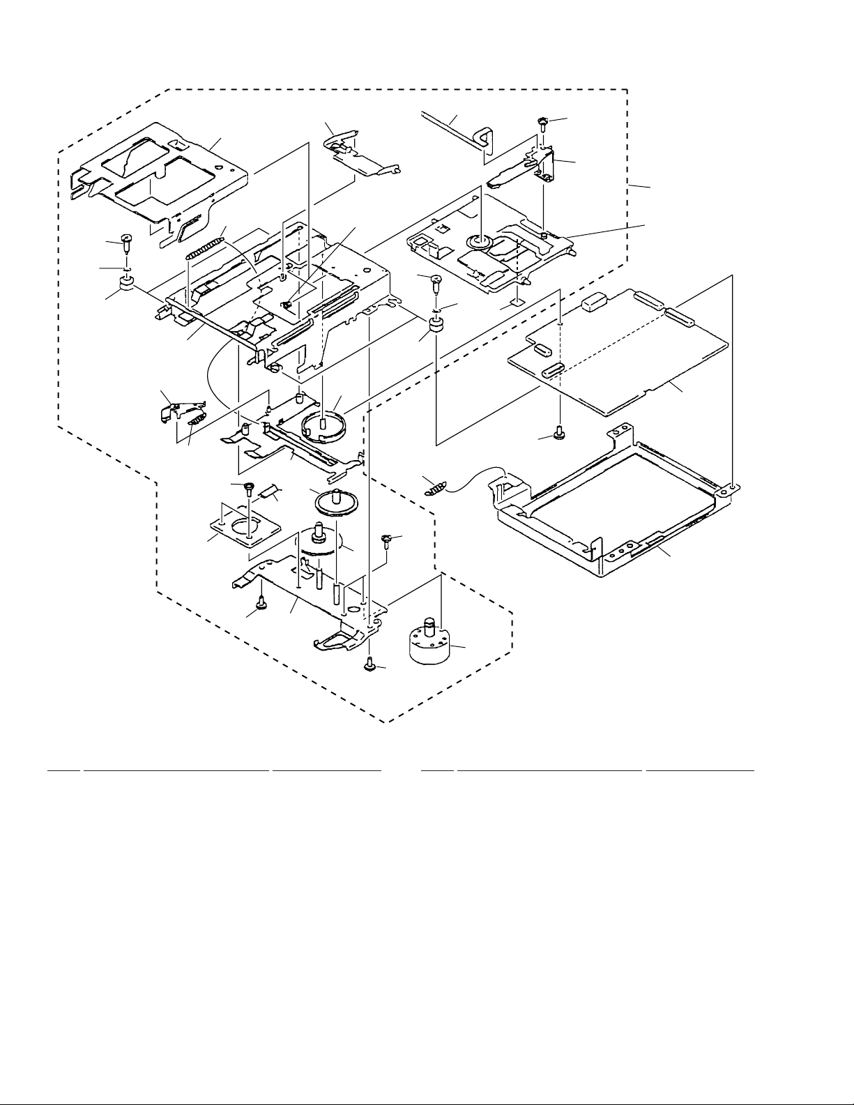
2. EXPLODED VIEWS AND PARTS LIST
NOTES:
2.1 PACKING
Parts marked by "NSP" are generally unavailable because they are not in our Master Spare Parts List.
The mark found on some component parts indicates the importance of the safety factor of the part.
Therefore, when replacing, be sure to use parts of identical designation.
Screws adjacent to mark on product are used for disassembly.
X-MDX707, XR-C2MD
(1) PACKING PARTS LIST
Mark No. Description Part No. Mark No. Description Part No.
1 Styloform F 4707900000
2 Styloform R 4707901000
3 Gift box See Contrast table (2)
4 Operating Instructions 4707920003
(English/Chinese)
5 Mirror Mat 4700915000
6 • • • • •
7 • • • • •
8 • • • • •
9 • • • • •
NSP 10 AA batteries (R6P) VEM-013
11 AM loop antenna 004690500013
12 Remote control unit
(CU-XR043) 0088041001
13 FM T-type antenna 004783500013
NSP 14 Polyethylene Bag AHG7030
15 • • • • •
16 Battery Cover AZA7331
(2) CONTRAST TABLE
X-MDX707/LBWXJ and NLWXJ/HK are constructed the same except for the following :
Part No.
Mark No. Symbol and Description X-MDX707 X-MDX707 Remarks
/LBWXJ /NLWXJ/HK
3 Gift box 4707911003 4707911002
3
Page 4
X-MDX707, XR-C2MD
2.2 UNIT ASSY (1/2)
1
4
8
9
CONTROL
PCB
2
15
8
Insulation
Plate
10
10P
7P
16
4P
A
2
15P
14
14P
12
7P
13
2
1
Refer to "2.5 MD UNIT".
11
Refer to "2.4 TOP PANEL ASSY".
2
2
Refer to "2.2 UNIT ASSY (2/2)".
20
18
19
2
3
7
8
17
6
POP Label
1
A
1
Refer to "2.3 FRONT UNIT".
1
2
5
8
4
Page 5
(1) UNIT ASSY (1/2) PARTS LIST
Mark No. Description Part No.
1 Screw CCZ30P060FMC
2 Screw BBZ30P080FZK
3 Rear Panel 4707810001
4 Side Panel L 4707814001
5 Side Panel R 4707815001
X-MDX707, XR-C2MD
NSP 7 Rear Label See Contrast table (2)
6 Tray Panel 4707807001
8 Screw BBT30P080FNI
9 CONTROL Unit 4707006000
10 Speaker Piezo CB13PA 002384700013
11 Wire Connector 14P (CN454) 4707561000
12 Wire Connector 15P (CN455) 4707562000
13 Flat Cable 4P 4707571000
14 Flat Cable 7P 4707573000
15 Wire Connector 7P 4707572000
16 Wire Connector 10P 4707574000
17 CD Label 4701855002
18 ANT Caution Label 4707854002
19 SP Caution Label 4707855002
20 Spacer 4707882000
(2) CONTRAST TABLE
XR-C2MD/LBWXJ and NLWXJ/HK are constructed the same except for the following :
Part No.
Mark No. Symbol and Description XR-C2MD XR-C2MD Remarks
/LBWXJ /NLWXJ/HK
NSP 7 Rear Label 4707850003 4707850002
5
Page 6
X-MDX707, XR-C2MD
2.3 UNIT ASSY (2/2)
40
19P
Double Face
43
42
43
28
42
Refer to "2.10
CD MECHA".
30
15P
36
28
39
2
42
28
43
38
IC PCB
6
13
5
28
Double
Face
48
14
DI PCB
4P
6
4P
11
10
7
49
4
AMP PCB
6
8
8
7
43
42
21
24
21
24
47
26
29
31
37
33
34
16P
32
2
23
44
20
27
2
16
CD
PCB
4P
35
6P
1
9P
5P
5P
17
22
18
19
46
45
17
PS PCB
15
25
2
41
29
3
3
6
Page 7
X-MDX707, XR-C2MD
(1) UNIT ASSY (2/2) PARTS LIST
Mark No. Description Part No. Mark No. Description Part No.
1 Cord Bushing 0064695000
2 Screw BBZ30P080FZK
3 Rubber Foot 4701881000
4 AMP Unit 4707001000
5 Heat Sink 4707720000
26 CD Unit 4707030000
27 PT Screw P2006SK 0972920065
28 Screw BPZ26P100FMC
29 Screw BPZ30P120FMC
30 CD Mecha,CMCF0210 4707150000
6 Screw IPZ30P120FMC
7 Screw BBZ30P080FZK
8 WL030140040B1 0987100600
9 • • • • •
10 H.S Bracket 4701273100
11 Heat Sink 4701720100
12 • • • • •
13 Wire Connector 4P (WC401) 4701576000
14 Wire Connector 4P (WC403) 4701576000
15 PS Unit See Contrast table (2)
16 Pin Terminal 0034473000
17 Fuse Holder,TP00351- 0045522000
18 AC Cord With Plug See Contrast table (2)
19 Cover,Spark Killer 0064644000
20 PT6AWG03T20 0950103020
21 Screw BSZ40P060FMC
22 Wire Connector 5P 4701565000
23 Rear Chassis 4701817000
24 Screw FBT40P060FZK
25 Himelon 4701898100
44 Fuse (F601) See Contrast table (2)
45 Fuse (F602/T5A) 0045049041
46 Fuse (F603/T2.5A) 0045023041
47 Power Trans (T601) See Contrast table (2)
NSP 49 Binder (BK-1) ZCA-BK1
31 CD Mecha Chassis 4701270000
32 Wire Connector 4P (CN805) 4707563000
33 Wire Connector 9P (CN806) 4707564000
34 Wire Connector 5P (CN807) 4701568000
35 Wire Connector 6P (CN804) 4701571000
36 CD Mecha Cover 4701819100
37 FFC 16P (CD-CD Mecha) 4701553000
38 Himelon 4701895000
39 FFC 15P (CD-CONT) 4701552000
40 FFC 19P (CD-CONTROL) 4701554000
41 Bottom Chassis 4701814000
42 ST Screw B2605SBK 0972726053
43 Cushion 4701897000
48 Screw BBZ30P080FNC
50 Fuse Label See Contrast table (2)
51 Fuse Label (T2.5A/L250V) 0074005174
52 Fuse Label (T5A/L250V) 0074005175
(2) CONTRAST TABLE
XR-C2MD/LBWXJ and NLWXJ/HK are constructed the same except for the following :
Part No.
Mark No. Symbol and Description XR-C2MD XR-C2MD Remarks
/LBWXJ /NLWXJ/HK
15 PS Unit 4707014000 4707012000
18 AC Cord With Plug 004701800005 004744300003
44 Fuse (F601/T1.6A) 0045017041 Not used
44 Fuse (F601/T800mA) Not used 0045013041
47 Power Trans (T601) (110V) 001950000005 Not used
47 Power Trans (T601) (220V) Not used 001947100005
50 Fuse Label (T1.6A/L250V) 0074005165 Not used
50 Fuse Label (T800mA/L250V) Not used 0074005176
7
Page 8
X-MDX707, XR-C2MD
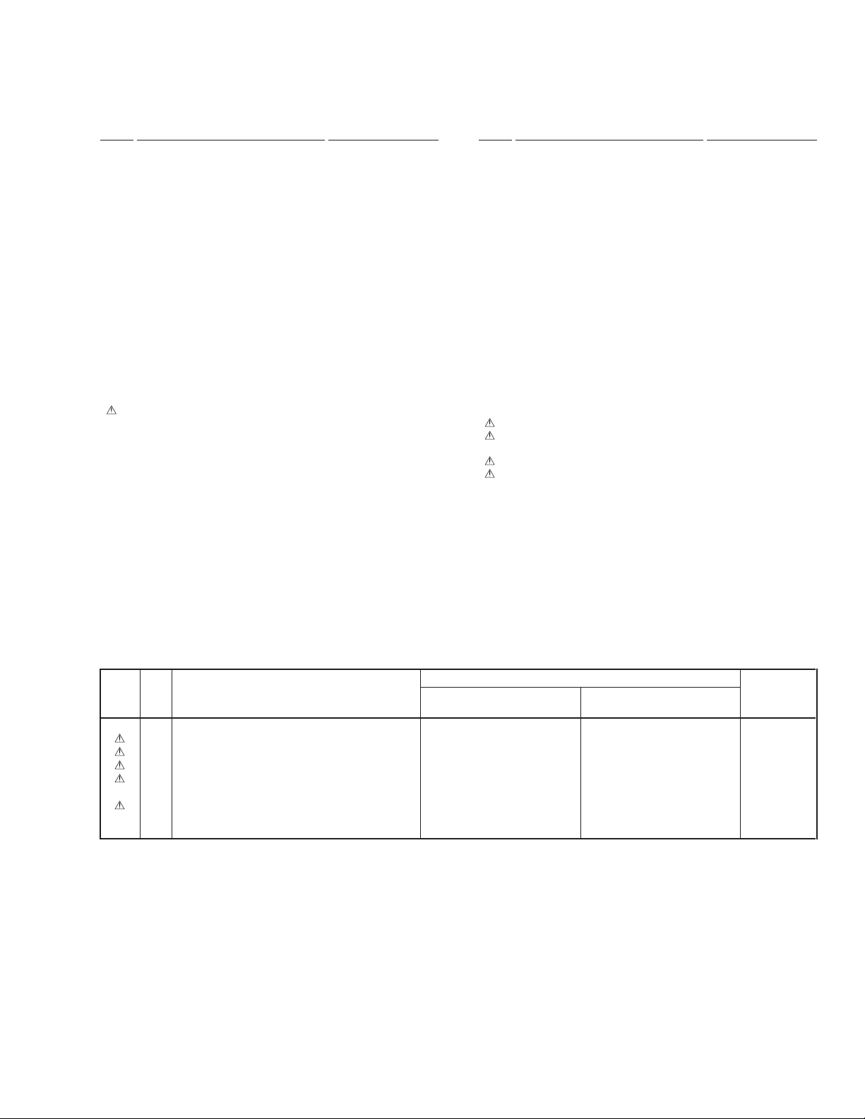
2.4 FRONT UNIT
1
30P
21
38
35
33
10
4
5
12
7
6
11
36
8
36
9
9
23
36
24
34
36
36
37
20
14
26
13
39
25
SW PCB
35
31
3
17
15
16
22
18
19
27
28
8
Page 9

X-MDX707, XR-C2MD
• FRONT UNIT PARTS LIST
Mark No. Description Part No. Mark No. Description Part No.
1 FFC 30P (FRONT-CONT) 4707550000
2 • • • • •
3 Screw 0979914200
4 LCD Holder 4707270000
5 Diffusion Plate 4707274000
NSP 25 HP PCB
21 Power Knob 4707863001
22 MD Eject Knob 4707864001
23 Cushion 4701896000
24 Shield Plate 4707816000
6 LCD Lens 4707271000
7 Reflector L 4707877000
8 Reflector R 4707878000
9 LED Spacer 4707880000
NSP 10 Double Face A 4701887000
NSP 11 Double Face B 4701888000
12 Diffusion Sheet 4707890000
13 Front Panel Set 4707800001
14 Enter Knob 4707879001
15 Function Knob Set 4707859001
16 Stop Knob 4707862001
17 AUX Knob 4707861001
18 CD Eject Knob 4707868001
19 CD Select Knob 4707869001
20 Volume Knob 4707865001
26 Volume Knob Ring 4707876001
27 Tact Knob A 4707866001
28 Tact Knob B 4707867001
29 • • • • •
30 • • • • •
31 Knob Cover 4707870001
32 • • • • •
33 FRONT Unit 4707035000
34 Front Chassis 4707812000
35 Screw CCZ30P060FMC
36 Screw BPZ26P100FMC
37 Screw TP2x6-SBK-C BPZ20P060FZK
38 LCD PANEL LMG172C1-F 004044100021
39 Stop Ring 4707401000
9
Page 10
X-MDX707, XR-C2MD
2.5 TOP PANEL ASSY
19
15
18
14
16
10
9
10
20
10
9P
6P
8
DECK PCB
21
13
Refer to "2.6 DECK
MECHA (1/2) FRONT"
AND
"2.7 DECK
MECHA
(2/2) REAR".
10
6
12
11
17
6P
5P
5
TUNER
PCB
422
7
10
10
3
2
22P
1
1
• TOP PANEL ASSY PARTS LIST
Mark No. Description Part No. Mark No. Description Part No.
1 Screw BBZ30P080FZK
2 FFC 22P (DECK-CONT) 4701556000
3 TUNER Unit 4707021000
4 Connector Plate SP 1600779000
5 Wire Connector 5P 4701569000
6 Wire Connector 6P 4701570000
7 DECK Unit 4707015000
8 Wire Connector 6P 4701563000
9 Lead Wire Clamper 0065375000
10 Screw BPZ30P120FMC
10
11 Gear 2401872000
12 Gear Holder 2401873000
13 Mecha Set,CRH34-07 4700100000
14 Lock Lever 4700281000
15 Lug Washer W/Wire 4701561000
16 COM Spring 4700400000
17 Up Case Spring 4701401000
18 Top Panel 4707803001
19 Up Case Set 4707804001
20 Deck Bracket 4701818000
21 Insulation Sheet 4701891000
22 Antenna Terminal 4P 003402900013
Page 11
X-MDX707, XR-C2MD
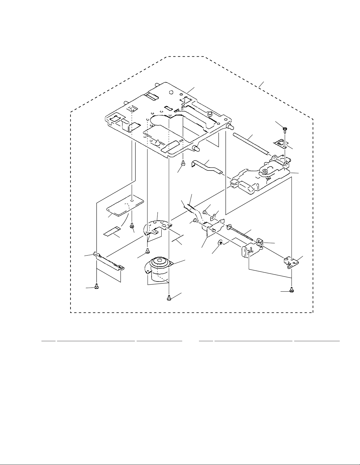
2.6 MD UNIT
Himelon
1
Refer to
"2.8 MD MECHA (1/2)
LOADING ASSY".
• MD UNIT PARTS LIST
1
1
2
4
1
1
1
Mark No. Description Part No.
1 ST Screw B2605SBK 0972726053
2 MD Mecha,KMK-260AAB GXX1155
3 MD Mecha Chassis 4707813000
4 MD Mecha Chassis 4701827000
5 MD Door Set 4750308004
6 Shaft 4750306000
7 EXT Spring 4750307000
8 WL030140040B1 0987100600
9 Wire Connector 11P 4701572000
10 FFC 11P (MD-CONT) 4701551000
11 FFC 19P (MD-MD Mecha) 4701555000
12 FFC 19P (MD-MD Mecha) 4701559000
13 Shield Plate 4750735000
14 MD Unit 4707025000
* GXX1155 is MD mechanism for service by which resistance
(R123, R213, R142) is removed from KMK-260AAB.
14
6
10
11P
5
7
3
15P
11P
9
13
12
11
19P
MD PCB
8
1
1
11
Page 12
X-MDX707, XR-C2MD
2.7 DECK MECHA (1/2) FRONT
18
21
27
17
34
23
24
13
2
1
3
10
25
30
12
29
36
38
11
5
4
31
16
15
22
26
7
37
10
6
32
33
9
35
28
8
20
19
14
• DECK MECHA (1/2) FRONT PARTS LIST
Mark No. Description Part No. Mark No. Description Part No.
12
1 Assy Holder Head 330934098
2 Frame Head 332193023
3 Lever Head 332593015
4 Spring Azimuth 161604032
5 Assy Lever Assist 330934055
6 Gear Arm Head 222394020
7 Chassis Head B 331123030
8 Eject Lock 332394024
9 Assy Arm Pinch R 330934060
10 Cap Reel 182283231
11 Arm UD 332393012
12 Assy Arm Pinch L 330934059
13 Arm Brake 332393014
14 Frame B 332113019
15 Assy Chassis 330933056
16 Frame C 332112020
17 Spring Cassette 331604031
18 Frame D 332112021
19 P.C.B Head 330704061
20 Housing S5BEH
NSP 31 Screw GSL20A2008
21 Spring 010804535
22 Spring 010814483
23 Spring 010814493
24 Spring 010804482
25 Spring 010804489
26 Spring 010814492
27 Spring 010804479
28 Spring 010824485
29 Spring 010824486
30 Screw 033004056
32 Screw 033004043
33 Screw GSE10A2004
34 Screw GSD20A2005
35 Washer GWN13X050040
36 Washer GWN13X060040
37 Washer GWN16X040050
38 Washer GWN15S040050
Page 13
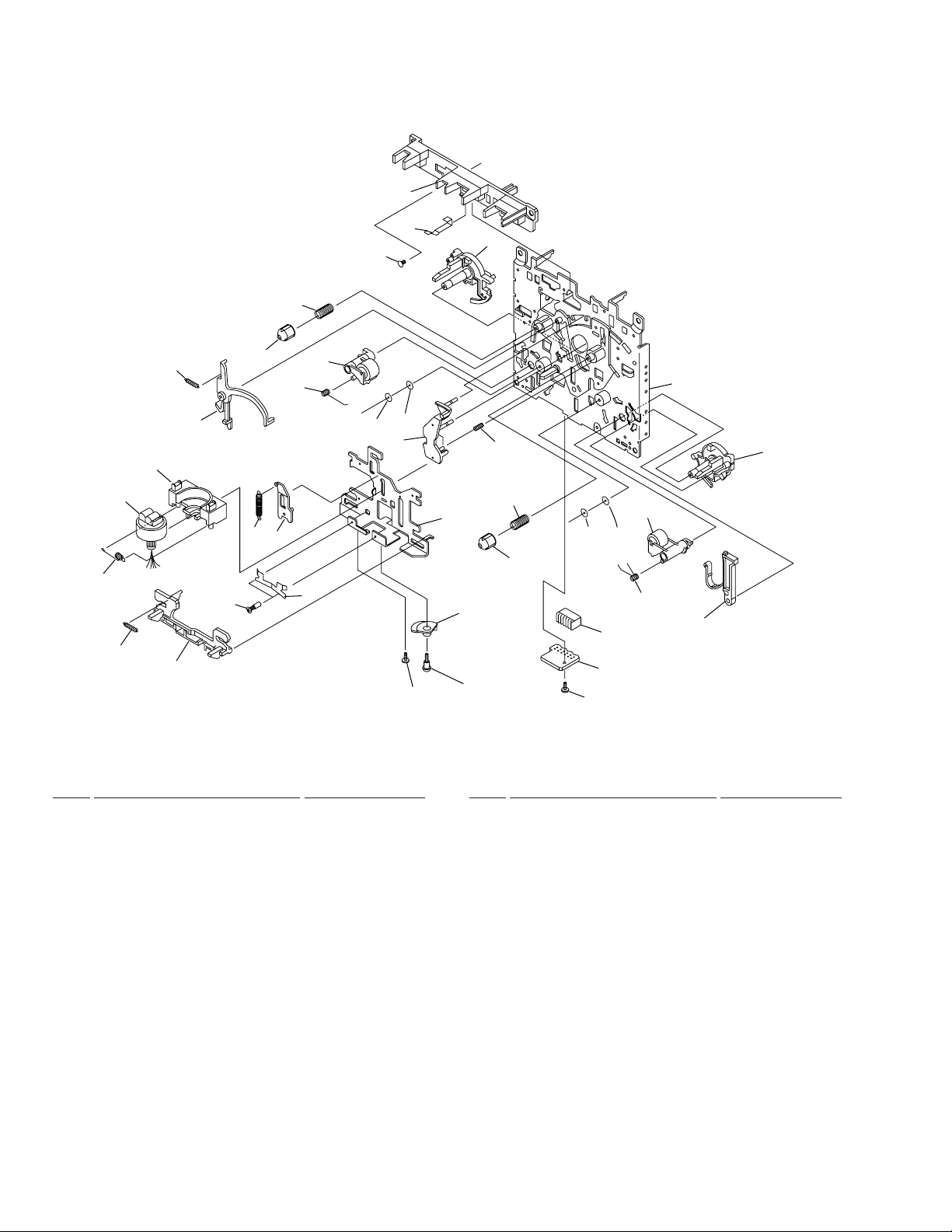
2.8 DECK MECHA (2/2) REAR
17
X-MDX707, XR-C2MD
18
30
19
5
1
2
28
4
33
3
ASSY CHASSIS
6
22
26
7
8
27
9
10
11
32
21
24
25
23
29
14
12
13
33
4
16
20
31
15
• DECK MECHA (2/2) REAR PARTS LIST
Mark No. Description Part No. Mark No. Description Part No.
1 K Plunger 033194259
2 Assy Coil 330934051
3 Plunger 033004338
4 Gear Reel 332224009
5 Arm Trigger 332683013
6 Assy Flywheel L 330934050
7 Gear Cam 332212010
8 Gear IDL 332224008
9 Gear REF 332224164
10 Assy Clutch 330933045
11 Gear P 332224002
12 Gear A 332224001
13 Gear FR 332224003
14 Arm FR 332393011
15 Assy Flywheel R 330934048
16 Belt 020844146
17 Bracket MM 332193025
18 Assy Motor 330934104
19 Wire 160724055
20 Assy P.C.B 330933147
NSP 22 9P Housing HBRK9R - 2
21 P.C.Board 330703035
23 Switch (Leaf) MTS10041MVLO
24 Photo Sensor SG105BC
25 Resistor ERDS2TJ681
26 Mode Switch MSW1722NCV
27 Refrector 330004140
28 Spring 010804480
29 Spring 010804543
30 Screw GSD20A2005
31 Screw 033004344
32 Screw GSP11A2605
33 Washer GWP18X060050
13
Page 14
X-MDX707, XR-C2MD
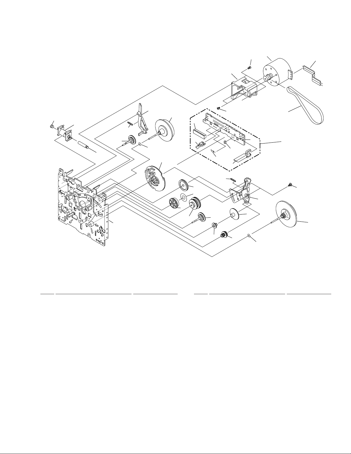
2.10 MD MECHA (1/2) LOADING ASSY
12
13
11
14
16
10
9
8
32
15
17
13
11
18
7
6
4
26
19
12
22
24
20
21
33
Refer to
"2.9 MD MECHA
(2/2) DECK
MECHA ASSY".
23
3
2
1
5
31
27
30
2
• MD MECHA (1/2) LOADING ASSY PARTS LIST
Mark No. Description Part No. Mark No. Description Part No.
NSP 1 Motor Plate Assy X-2646-247-1
2 Screw +P2.6×4.5 TYPE3 7-627-854-28
3 L-SW Mount Board 1-668-261-11
4 Wire Flat Type (6p) 1-783-386-11
5 Gear (Relay B) 2-646-555-02
6 Gear (Relay A) 2-646-554-01
7 Slot Frame Assy X-2646-249-2
8 Spring (Slot Arm) 2-646-563-01
9 Arm Slot 2-646-556-01
NSP 10 Road Frame Assy X-2646-248-2
11 Insulator 2-646-548-01
12 Screw 7-688-002-11
13 Screw Step 4-628-167-01
NSP 14 Frame Slide 2-646-557-01
15 Arm Head 2-646-559-01
NSP 22 Sheet Double-Fase 2-646-549-02
NSP 23 MD MOUNT A-4917-020-A
NSP 27 Flame Main 2-646-547-02
NSP 33 Loading Assy A-4912-117-A
19 PWB Head Flexible 1-669-181-11
20 Grip +P1.7×2.5TYPE2 2-627-529-01
21 Over Write Head 1-550-518-12
24 Screw Toothed Lock 2-643-228-01
25 • • • • •
26 Spring (Door Arm) Tension 2-646-545-01
28 • • • • •
29 • • • • •
30 Loading Motor Assy X-2626-328-1
31 Screw +P1.7×1.8TYP.3 7-627-852-38
32 Screw +P2×3 TYP.3 7-627-553-37
14
16 Spring Tension Coil 2-646-562-01
(Slot Frame)
17 Spring SP Tension 2-646-561-01
(Arm Head)
18 Cam Mode 2-646-560-01
Page 15
2.11 MD MECHA (2/2) DECK MECHA ASSY
6
X-MDX707, XR-C2MD
23
12
11
13
8
1
9
10
7
5
4
3
2
1
4
15
25
19
18
15
14
20
21
16
17
1
24
22
• MD MECHA (2/2) DECK MECHA ASSY PARTS LIST
Mark No. Description Part No. Mark No. Description Part No.
1 Grip +P1.4×3.5TYPE3 2-627-404-01
2 Guide Sub 2-646-453-01
3 Wire Flat Type (7P) 1-783-387-11
4 Screw+P1.4×1.8TYPE3 7-627-850-79
5 D-SW MOUNT BOARD 1-668-262-11
16 SL Motor Assy X-2626-329-1
17 Gear (MD) 2-646-571-01
18 Screw +P1.7×4 TYPE3 7-627-852-18
19 SP Motor Assy X-2626-327-1
20 Lead Screw Assy X-2626-330-1
NSP 6 Shassis Mechanical 2-646-575-01
7 Bracket SP Motor 2-646-566-01
8 PWB OP Flexible 1-669-180-11
NSP 9 Wire SL Motor Lead 1-783-318-11
NSP 10 Wire SL Motor Lead 1-783-318-21
11 Shaft Guide 2-646-452-01
12 Grip +P1.4×1.4TYPE2 2-627-530-01
13 Rack (Inserter) 4-963-914-02
14 Plate Pre Road 2-646-567-01
15 Screw (1.2×3.3) 2-627-431-01
21 Lead Holder Assy X-2626-331-1
22 Holder (B) Lead 2-646-573-01
NSP 23 Deck Mecha Assy A-4912-118-A
24 Devise, Mini Disc KMS-260A
25 Spring SP Tension 2-646-564-01
15
Page 16
X-MDX707, XR-C2MD
2.12 CD MECHA
9
9
6
9
47
39
25
26
22
3
69
67
18
71
33
71
66
73
57
73
41
2
40
39
61
53
23
58
37
66
53
65
1
49
52(3/7)
48
24
50
80
51
54
21
38
52(2/7)
52(1/7)
29
55
27
71
31
66
36
17
52(6/7)
16
5
54
52(7/7)
59
68
32
15
72
28
30
42
14
45
43
75
4
74
43
79
46
78
8
9
44
43
43
46
45
70
16
77
58
61
63
52(5/7)
35
60
60
34
63
59
56
52(4/7)
62
53
11
20
19
12
10
13
Page 17

X-MDX707, XR-C2MD
• CD MECHA PARTS LIST
Mark No. Description Part No. Mark No. Description Part No.
1 Chassis 45-210-2317
2 Drawer 45-264-2004
3 Assy Holder L 45-093-4088
4 Assy Holder R3 45-264-3278
5 Assy Gear Drive 45-093-4075
41 Cushion 45-063-4136
42 Frame S 45-211-3072
43 Rubber Cushion SO 45-063-4072
44 Pick-up Unit KSM213CCM
45 Spring 01-081-4561
6 Assy Carriage 100 45-093-4189
7 • • • • •
8 Bevel Gear 4 45-222-4214
9 Assy Gear Star 45-093-4084
10 Shaft 45-300-4018
11 Cap 45-262-4019
12 Gear Spring 45-222-4021
13 Bevel Gear 1 45-222-4059
14 Gear Idler 1 45-222-4026
15 Gear Idler 3 45-222-4067
16 Bevel Gear 3 45-222-4061
17 Pulley C 45-222-4058
18 Pulley B 45-229-4053
19 Holder 2 45-219-4062
20 Holder 1 45-219-3055
21 Slider 1 45-259-2031
22 Slider 2 45-259-3066
23 Arm Stopper A2 45-239-4279
24 Arm Stopper B 45-239-4065
25 Gear Idler A 45-222-4049
26 Gear Idler C 45-222-4051
27 Lever 45-259-3008
28 Clamper A 45-229-3024
29 Lifter 45-259-3025
30 Arm 45-239-1037
31 Magnet 36-067-4928
32 Clamper B 45-229-3069
33 Pulley A 45-222-4052
34 Pulley Motor 23-226-4031
35 Pulley Motor 23-226-4096
46 Spring 01-081-4562
47 Assy Carriage 200 45-093-4190
48 Assy Carriage 300 45-093-4191
49 Plate E 45-219-4107
50 Spacer SW 45-219-4127
51 Connector 04FM-1.0SP
52 PC Board 45-070-3074
53 Switch MPU10101MMB0
54 Switch MPU20273BLB0
55 Connector 04FM-1.0ST
56 Connector S4BEH
57 Card Wire 45-072-4077
58 Wire 45-070-4080
59 Wire 45-072-4078
60 Wire 45-070-4081
61 Wire 45-072-4079
62 Connector S9BEH
63 Motor RF500TB14415
64 • • • • •
65 Rubber Cushion 45-063-4115
66 Shaft 03-300-4404
67 Shaft 03-300-4403
68 Shaft 03-300-4409
69 Spring 01-082-4577
70 Washer GWP23X055025
71 Washer GWP15X045025S
72 Screw GSL20A2010
73 Screw GSL10B2006
74 Washer GSN31X120050
75 Screw 03-300-4366
36 Spring 01-000-4541
37 Spring 01-082-4558
38 Spring 01-082-4559
39 Belt 02-083-4157
40 Belt 02-083-4152
76 • • • • •
77 Screw GSP14A2604
78 Screw GSL20A2610
79 Washer 03-000-4427
80 Screw GSL15A2005
17
Page 18
1
23
X-MDX707, XR-C2MD
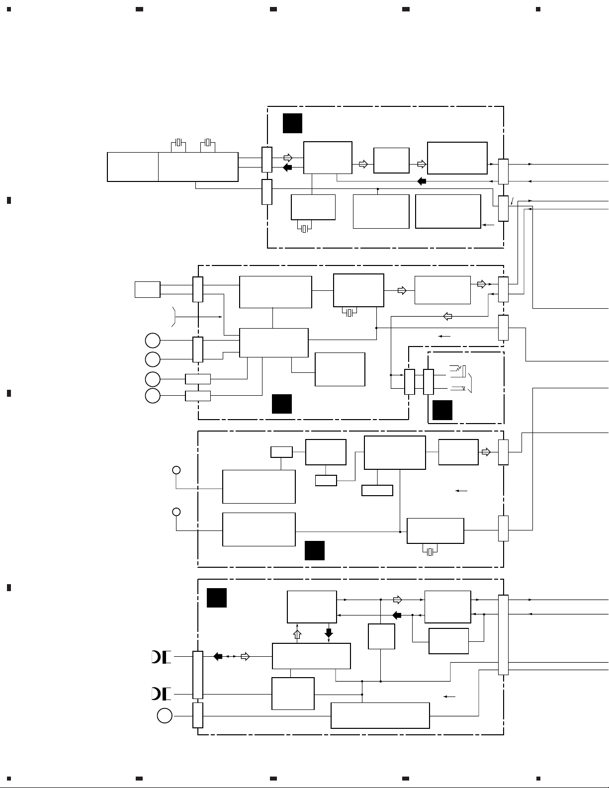
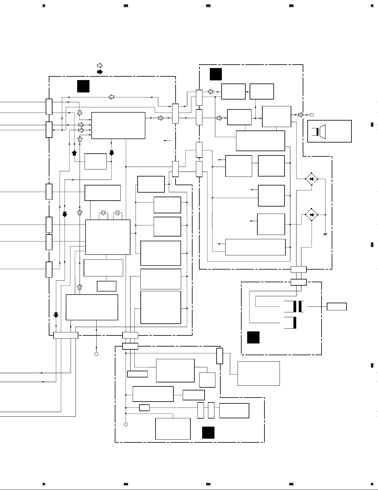
3.BLOCK DIAGRAM AND SCHEMATIC DIAGRAM
3.1 BLOCK DIAGRAM
A
4
• MD MECHA
MD MECHA
GXX1155
20MHz 32kHz
MD CONTROL MICON
8-759-533-77
(RU8X12MF-0030)
5
1
CN502CN501
MD UNIT
D
AD/DA
15
0911505000
12
(PCM3003)
XTAL OSC
IC502
TC7WU04FU
X501
22.5792MHz
IC503
19
6
TEMP-SENSOR
0911110000
(BA10358)
FILTER
IC504
BA4510F
IC505
MUTE
Q502 DTA114EK
76
Q503,Q504
DTC114TK
+3.3V REG.
IC501
0911209300
(S-81340HG-KJ-X)
11
Vcc3
3
P.B
REC
CN503CN504CN801
CONT
• CD MECHA
FOCUS/TRACKING
B
PIC
TRACKING
FOCUS
SPINDLE
MOTOR
SLED
MOTOR
CARRIAGE
MOTOR
DRAWER
MOTOR
M
M
M
M
CN803
CN804
CN805
CN805
1,2
3,4
1,2
3,4
1,2
3,4
SERVO
IC803 0911168502
(CXA1782BQ)
POWER DRIVER
IC802 0911209400
(BA5936S)
14,15
30,31
CD UNIT
C
31
1-CHIP
36
PROCESSOR
IC804
CXD2508AQ
X801
16.1344MHz
CD +5V REG.
Q801
0906209425
(2SA966Y)
5,
69,
70
LOW-PASS
6
FILTER
IC801 BA4510F
3
42
CN807
3
CN750
B
Vcc2
J700
PHONES
HP PCB
77
3
CN802WC1WC2CN302
5
FM: IF/DET/MPX
24
AM: RF/IF/DET
IC1 0911209800
(TA2099N)
AM OSC
TPSS
IC302
BA335
13
20
PLL
IC2 0911177300
(TC9216P)
4.5MHz
14
DOLBY-B
99
0911200400
(CXA1552P)
BA15218N
19kHz BP
Q7,Q8
2SC1740S
X1
IC304
ALC
IC305
Vcc4
Vcc1
11
16
1
8
6
19
IF AMP
CF-1
FM ANT
C
AM LOOP
ANT
RF1
FM TUNER MODULE
8
0039654000
(TFF-J2-J-559A)
RF2
AM RF TUNING UNIT
12,13
0039640000
(RBW07VB)
E
• DECK MECHA
REC/P.B
HEAD
D
ERASE
HEAD
MOTOR
M
DECK UNIT
1
CN301CN303
5
1
P.B-REC AMP
P.B
P.B/R.P SWITCH
Q101,Q102,Q201,Q202
BIAS
Q306,Q311
0906202003
(2SD467)
Q1
2SC1740S
CF-3
8
A
IC301
0911166600
(TA8142P)
8
11
2SJ103
TUNER UNIT
REC
C-MECHA GAVANA REG.
Q319 0900008725 (2SA1359)
Q320,Q322,Q325 DTC114TS
18
1234
Page 19
5
678
X-MDX707, XR-C2MD
3
11
CN452CN450CN460CN459CN451 CN458
9
13
5
Q450 DTA114TK
Q451 2SC2412K
Q650,Q750 0906505419
Q651,Q751 2SD1302
15
17
CN453
: PB SIGNAL
: REC SIGNAL
F
CONTROL UNIT
FUNCTION/
16
SOUND/VOLUME
17
19
21
REC AMP
IC452
BA15218N
MD INTERFACE
TC74HCT08AF
MICROCOMPUTER
(CXP740096-109Q)
BUZZER DRIVER
Q459 0906505419
(2SD1757K)
TAPE/LINE SW
19
LINE IN
IC450
LC75394NED
(REC)
31
IC901
X901
X900
16MHz
32kHz
IC900
0037502200
BUZZER
BU450
58
PS DET 0
Q911,Q913
2SC2412K
IC903 0911186600
(S-81350HG)
Q903 2SC2412K
Q904 2SA1037K
CN461
CN700
KEY LED
DISC LED DRIVER
Q700 – Q702
2SC2412K
KEY
VR
JOG
13
11
7
Vcc4
PS DET 1
Q912,Q914
2SC2412K
RESET
IC902
0911851600
(S-80727AN)
REG. +5V
LED DRIVER
Q456 0900008725
(2SA1359Y)
Q457 2SC2412K
LED FILTER
Q905-Q907,
Q915-Q917
0906505419
(2SD1757K)
Q908-Q910
2SC2412K
BACK-LIGHT LED
DRIVER
Q703 – Q708
0906505319
(2SD1963-S)
REMOCON REC
RM700
0039648000
(SPS-444-1)
CN454CN455
DISC-LED
1–3
G
AMP UNIT
2
4
CN406 CN405 CN401
CN400
BACKLIGHT
LED
JW700
Q152,Q252
2SD1302
2
Vcc1
Vcc4
LD700
4-DIRECTION
TACT SW
JW701
I
FRONT UNIT
MUTE
S-MUTE
Q150,Q250
2SD1302
TUNER +5V
Q400
0906202003
(2SD467)
Q403,Q407,Q415 2SC2412K
Q406 0900008725(2SA1359)
H.P. AMP
1
IC400
BA15218N
2
POWER AMP
2
IC401
0911209600
(LA4663)
POWER-AMP CONT.
(ST-BY) AND (MUTE)
Q416,Q417 2SC2412K
Q418 DTA114TK
TUNER +9V
Q401
0906209425
(2SA966)
Vcc2
Vcc3
AUDIO REG. (+8V)
CD +7.8V
IC402
0911209700
(PQ20RX11)
MD +5V
IC403
0911209700
(PQ20RX11)
H
PS UNIT
LC700
LCD PANEL
004044100021
S723
14
CN403
WC601
POWER
TRANSFORMER
LBWXJ TYPE
: 001950000005
NLWXJ/HK TYPE
: 001947100005
D423
0913013600
(KBU603)
16V
D424–D427
2626323000
(1N5401TM)
11V
T601
SPEAKER
TARMINAL
SPEAKER
6Ω
(15W)
AC IN
A
B
C
D
19
5
6
7
8
Page 20
1
23
X-MDX707, XR-C2MD
3.2 OVERALL CONNECTION DIAGRAM
A
MD MECHANISM (GXX1155)
MD MOUNT (A-4917-020-A)
CN103 CN102
123456789
J
10111213141516
123456789
4
10111213141516
171819
STB
VBAT
LEDO
SYS+3.3V
123456789
AMUTE
P DOWN
SYS RST
TXD
RXD
DARST
XLATCH
10111213141516
RTS
CTS
SCLK
ADDT
SWDT
EMPHASIS
123456789
BCK
MGND
DADT
MGND
M+5V
M+5V
LRCK
DIN
H+5V
GSYS
GSYS
3.3VOUT
10111213141516
DOUT
+5VSYS
512FS
+5VSYS
171819
HGND
256FS
CN501 CN502
MD UNIT
D
(4707025000)
CN504 CN503
123456789
VC
1
+5V
2
3
4
B
C
Chassis
5
6
7
8
GND
9
LD
10
VR
11
PD
12
F+
13
T+
14
15
16
SP+
1
SP–
2
SL+
3
SL–
4
LIMIT
5
GND
(4707150000)
6
CD MECHANISM
1
2
3
4
1
2
3
4
5
6
7
8
9
CARR–
CARR+
DRAW–
DRAW+
SW8
SW7
SW6
SW5
SW4
SW3
SW2
SW1
SWGND
CN803
1
2
E
3
D
4
A
5
B
6
C
7
F
8
C
9
10
CD UNIT
11
12
(4707030000)
13
14
T–
15
F–
16
CN804
1
2
3
4
5
6
CN805
1
2
3
4
CN806
1
2
3
4
5
6
7
8
9
123
CN801
CN802
4
1
2
3
4
5
6
7
8
9
10
11
12
13
14
15
1
2
3
4
5
6
7
8
9
10
11
12
13
14
15
16
17
18
19
HP Rch
HP GND
HP Lch
HP SW
CD Rch
PRIGND
CD Lch
GND
GND
+7V
+7V
GND
FCD
GND
DIN
SW0
SW1
SW2
SW3
SWGND
CTL1
CTL2
CTL3
CTL4
CLK
XLT
DATA
XRST
SENS
NC
SQCK
SQSO
SCOR
GND
15
14
13
12
11
10
9
8
7
6
5
4
3
2
1
1
2
3
4
5
6
7
8
9
10
11
12
13
14
15
16
17
18
19
CN450
CN459
CN451CN807
123451
RTS
GND
TEMP
DOUT
D GND
123456789
P DOWN
CN460 CN452
CN458 CN453
12345
10
11
TXD
CTS
RXD
RESET
MDREC
10
11
F
CONTROL UNIT
(4707006000)
6
123456789
MD+5V
Lch OUT
Rch OUT
F F
1/2, 2/2
22212019181716151413121110
MDH+5V
MDM+5V
MDA GND
123456789
MDH GND
MDM GND
Rch REC
REC GND
10
11
Lch REC
10
11
987
654
321
Lch
SW
Rch
GND
GND
12345
B
HP PCB
D
+9V
+5V
L ch
R ch
GND
5
PERIOD
234
WC1 WC2
TUNER UNIT
A
(4707021000)
TDATA
CLOCK
TUNING
12345
GND
STEREO
6
+11V
A +8V
A GND
PRIGND
123456789
LchREC
RchREC
LchPB
RchPB
CN302CN750
E
CN301 CN303
HEAD.
GND
12345
Lch
Rch
12345
6
GND
GND
COM.
E HEAD
6
DECK MECHANISM
TPSS
DOLBY
BEAT CUT
REC/PLAY
REC/MUTE
DECK SW3
10111213141516
DECK UNIT
(4707015000)
123456789
HALF
REC F
REC R
123456789
DECK SW2
DECK SW1
DECK SW0
171819
NC
PHOTO
SOLENOIDO
PHOTO
MOTOR
REPEAT
SOLENOIDO
202122
VCC
MODE
P GND
CONT.
BIAS
(4700100000)
20
1234
Page 21
5
678
X-MDX707, XR-C2MD
Note : When ordering service parts, be sure to refer to "EXPLODED VIEWS and PARTS LIST" or "PCB PARTS LIST"
LC700 LCD PANEL
(004044100021)
E
RS
RW
DB0
DB1
DB3
DB2
DB4
DB5
DB6
VSOUT
LCDVCC
LCDGND
123456789
LD700
FRONT UNIT
I
(4707035000)
CN700
302928272625242322212019181716151413121110
VCC
GND
KEY1
KEY0
KEY2
DISC3
DISC2
DISC1
VJOG0
REMOCON
PWP-KEY
123456789
VJOG1
KEY3
LEDVCC
1011121314151617181920212223242526
LEDGND
CN461
DB7
1011121314
BLCONT B
BLCONT R
BLCONT G
LCDGND
RS
98765
E
RW
DB0
JW700
1
1
JW701
KEY PCB
DB1
DB2
DB3
DB4
27 4
2
2
DB5
28 3
DB6
29 2
A
DB7
30 1
B
PS UNIT
H
(LBWXJ TYPE
: 4707014000)
(NLWXJ/HK TYPE
: 4707012000)
CN455 CN454
13
14
151
MDS GND
MDH GND
MDM GND
23456
10
11
12
MD+5V
MDH+5V
MDA GND
NC
MDM+5V
TUNERGND
7
TUNER+5V
TUNER+9V
CDPRIGND
12345
123456789
NC
CDGND
CD+8V/+7V
6
10
11
12
13
141
L ch
R ch
ACDET
PSCONT
GND
HP SW
HP Lch
HP Rch
HP GND
FTUNER
2345612345678
A GND
S MUTE
+11V
A +8V
123456789
CN400 CN406 CN401 CN405 CN403
AMP UNIT
G
(4707001000)
WC401
123
123
WC404
IC PCB
4
4
WC403
123
123
WC406
DI PCB
4
4
WC601
12345
GND
AC16V2
AC16V1
12345
AC11V2
AC11V1
CN402
Lch 1
Lch 2
Rch 1
Rch 2
NEUTRAL
1
2
3
4
LIVE
SPEAKER
LBWXJ
AC110V
NLWXJ/HK
AC220V
AC POWER CORD
LBWXJ
: 004701800005
NLWXJ/HK
: 004744300003
C
D
21
5
6
7
8
Page 22
1
X-MDX707, XR-C2MD
23
4
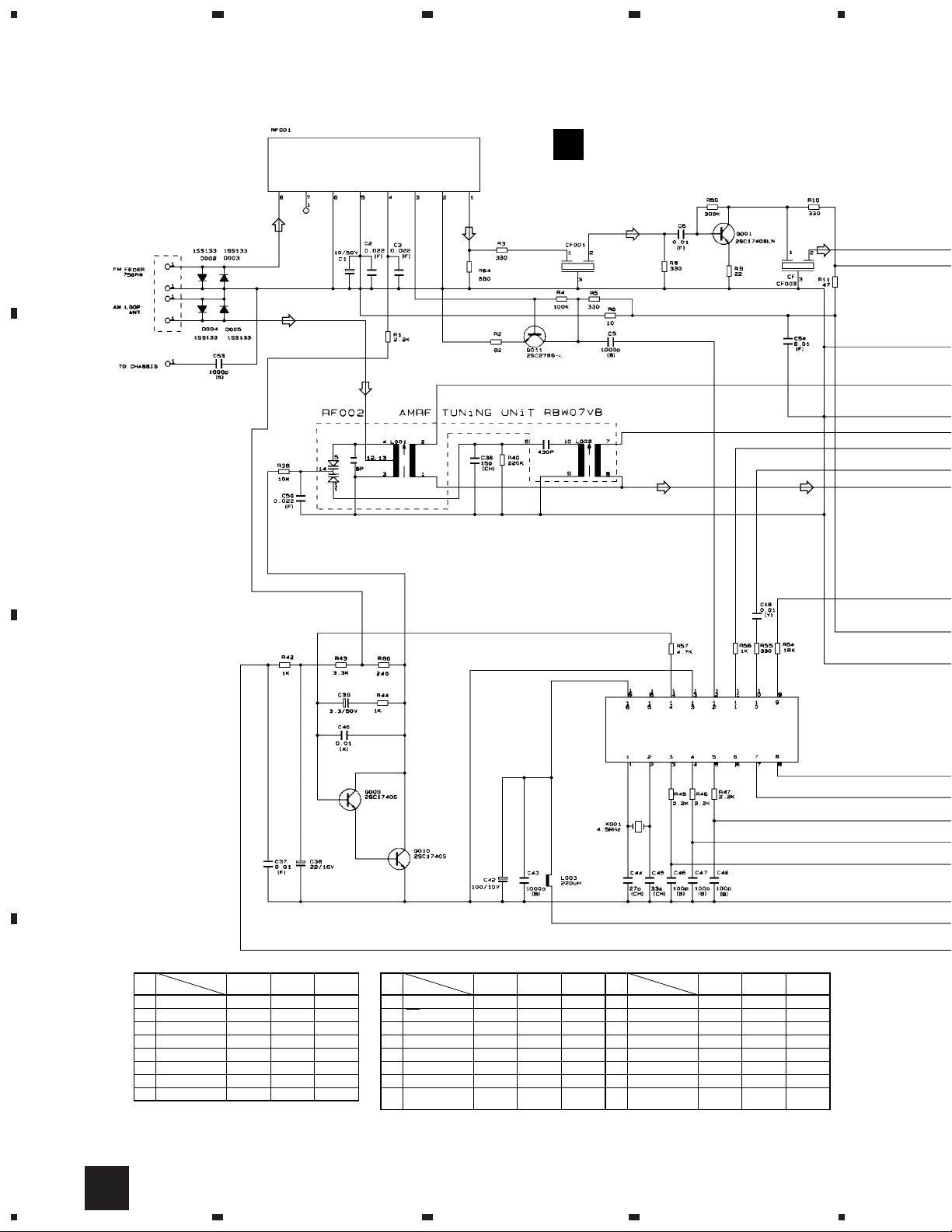
3.3 TUNER UNIT
A
B
003402900013
AT1
0039655000
(FM)
(AM)
RF MODULE
0039640000
(AM)
(FM)
TUNER UNIT (4707021000)
A
0039067000
(FM)
(AM)
(FM)
0039067000
(AM)
IC002 0911177300
(TC9216P)
C
0038168000
RF001
Pin
No.
D
Condition
Pin Nane
1
20GND 0 0
3 1.1F OUT 1.1 0
4 1.1VT ––– 7.1
5 7.6VCC 7.6 0
60GND 0 0
70ANT 0 0
8 –––––––– ––– –––
FM NO
Signal
0IF OUT
FM ST
00
AM NO
Signal
(V)
IC002
Pin
No.
Condition
Pin Nane
1
2 2.4XT 2.4 2.4
3 4.6DATA 4.6 4.6
4 4.6CLOCK 4.6 4.6
5 4.6PERIOD 4.6 4.6
6 000
7 4.8AM/FM (H-FM) 4.8 0
FM ST. VCO
8 4.8
STOP (H-ST)
FM NO
Signal
2.3XT
FM ST
AM NO
Signal
2.3 2.3
4.8 0
Pin
No.
Condition
Pin Nane
9
10 2.5IF IN 2.5 2.5
11 0AM IN 0 2.5
12 2.2FM IN 2.2 0
13 0GND 0 0
14 1.1DO1 1.1 1.1
15 0DO2 0 4.9
16 4.9VCC 4.9 4.9
FM NO
Signal
0IF CONT
AM NO
FM ST
Signal
00
(V)
22
A
1234
Page 23
(AM)
(AM)
(FM)
0012340000
5
678
X-MDX707, XR-C2MD
(T)
: TUNER AUDIO SIGNAL ROUTE
(FM)
(AM)
0039155000
IC001 0911209800
(TA2099N)
(T) (T)
: FM SIGNAL ROUTE
(AM)
: AM SIGNAL ROUTE
(T)
(T)
L4,L5 :
0039876000
A
B
0906222500
2/2
F
CN451
WC1
4701569000
4701570000
WC2
1/2
F
CN458
IC001
Pin
No.
Condition
Pin Nane
1
2 3.2FM BW 2.4 1.9
30FM VL SENS 0 0
4 2.0AM OSC 2.0 2.0
5 1.3FM IF SENS 1.3 1.6
6 5.0VCC 5.0 5.0
7 1.3AGC 1.5 1.2
80GND 0 0
9 1.6IF OUT/CONT 1.6 1.6
10 5.0TUN IND. 0 5.0
11 5.0ST. IND. 0 5.0
12 1.0Rch OUT 1.0 1.0
13 1.0Lch OUT 1.0 1.0
14 0.6VCO 0.7 0
LPF2
15 3.4
(GND-MONO)
LPF1
16 3.0
(GND-AM)
17 1.2MPX IN 1.2 1.2
18 1.1AM DET OUT 1.3 1.3
19 2.3FM DET OUT 1.6 1.9
20 1.8FM QUAD 1.8 2.1
21 2.0AM IF IN 2.0 2.0
22 2.0V stb 2.0 2.0
23 5.0AM MIX OUT 5.0 5.0
24 2.0FM IF IN 2.0 2.0
FM NO
Signal
2.0AM RF
FM ST
2.0 2.0
3.4 0.5
3.0 0.6
AM NO
Signal
(V)
C
D
A
5
6
7
8
23
Page 24
1
X-MDX707, XR-C2MD
3.4 HP PCB, CD UNIT
23
A/D
(V) SW0
0.00~2.00 : (ACCIDENT)
2.01~2.78 :
2.79~3.36 :
3.37~4.00 :
4.01~5.00 : C.EXT/C.HOM C.No1/C.No.2
D.OPN/D.CLSE
D.OPN SW
D.CLS SW
SW1
C.HOME SW
C.EXT SW
(NO USE)
SW2
C.No1 SW
C.No2 SW
SW3
S.FWD/S.REV
S.FWD SW
S.REV SW
CD UNIT
C
(4707030000)
4
SW1 : COMMON
SW1 : DRAWER OPEN DETECT SW
SW2 : CARRIAGE EXTRA POSITION SW
SW3 : CARRIAGE HOME POSITION SW
SW4 : CARRIAGE NUMBER SW
SW5 : CARRIAGE NUMBER SW
SW6 : DRAWER CLOSE DETECT SW
SW7 : SLIDER FORWARD POSITION SW
SW8 : SLIDER REVERSE POSITION SW
A
(CD)
4707564000
CN806
CN803
(CD)
(CD)
(CD)
(CD)
(CD)
(CD)
CD MECHANISMCD MECHANISM
0034887016
B
TP5
TO
TP4
FO
TRACKING
BALANCE
TP3
TEO
0031781503
0031781203
FOCUS
OFFSET
(CD)
(CD)
TP1
VC
(CD)
IC803
0911168502
(CXA1782BQ)
(CD)
(CD)
(CD)
TRACKING
GAIN
0031781203
0
0031781103
FOCUS
GAIN
180k
TP2
RFO
(CD)
C
CN804
15k
4701571000
0911209400
CN805
4707563000
HP PCB
B
003352100001
D
PHONES
0034751005
(HP)
FB750
D750,D751 : 1SS133
CN750
CN807
(HP)
4701568000
Q801 : 0906209425
24
B
C
1234
Page 25
5
678
X-MDX707, XR-C2MD
(CD)
: CD AUDIO SIGNAL ROUTE
(HP)
: HP AUDIO SIGNAL ROUTE
(CD)
(CD)
D804,D805,D812
: MTZJ5.1B
IC804
CXD2508AQ
(CD)
(CD)
X801 : 16.1344MHz
0038136000
CN802
0034887019
A
CN459
1/2
F
B
(CD)
(CD)
(CD)
(CD)
(2/2)
C800
4P
(CD)
(CD)
(CD)
(CD)
(CD)
(1/2)
(CD) (CD)
(CD)
(CD)
(HP)
CN801
C
CN450
2/2
F
0034887015
D
C
5
6
7
8
25
Page 26
1
X-MDX707, XR-C2MD
3.5 MD UNIT
A
23
MD UNIT (4707025000)
D
4
EF512:
0011612203
DTF1067
CN103
B
C
J
(MD)
CN501
0034688016
(MD REC)
(MD DI)
(MD REC)
(MD DI)
(MD REC)
(MD DI)
(MD
REC)
0911209300
0911505000
DTF1067
DTF1067
(MD)
DTF1067
(3/3)
(MD)
0011813000
(MD)
(MD)
DTC114EK
(MD REC)
(MD DI)
(1/3) (2/3)
DTF1067
X501 : 22.5792MHz
0038204000
J
CN502
0034688019
CN102
L510,L511 :
0991401005
FB501,FB502 :
0011813000
JP545, JP587: 0011813000
D
26
D
1234
Page 27
5
678
X-MDX707, XR-C2MD
A
(MD)
(MD REC)
DTA114EK
DTC114TK
(1/2)
: MD AUDIO SIGNAL ROUTE
: MD REC ANALOG AUDIO SIGNAL ROUTE
(MD DI)
: MD REC FROM CD DIGITAL AUDIO SIGNAL ROUTE
EF501-EF511:
0011612203
(MD)
SHIELD PLATE
47050735000
(MD)
(2/2)
(MD REC) (MD REC)
(MD DI)
R650
10(1/4W)
DTC114TK
(MD)
(MD)
(1/2)
0911110000
(MD DI)
R530
4.7k
R529
2.7k
(MD REC)
CN503
4701572000
CN504
0034887011
2/2
F
CN452
1/2
F
CN460
B
C
0918004400
0911110000
(2/2)
D
D
5
6
7
8
27
Page 28
1
X-MDX707, XR-C2MD
3.6 DECK UNIT
23
4
A
DECK
MECHANISM
B
CN301
4701563000
(PB)
(PB)
(REC) (REC)
(PB)
0906222500
(REC) (REC)
(PB)
(PB)
(PB)
(PB)
0911166600
0990415624
(REC)
0990415624
(PB)
0906202003
0015083000
REC
BIAS
0031781103
0906202003
0906222500
C
CN305
0034210003
Normal condition PLAY MODE.
( ) : Condition REC MODE.
DECK UNIT (4707015000)
E
(PB)
(REC)
(PB)
(REC)
D
0034688022
CN302
CN453
2/2
F
28
E
1234
Page 29
(REC)
5
678
X-MDX707, XR-C2MD
A
(REC)
(PB) (PB)
(PB)
(REC)
(REC)
(REC)
(PB)
Rch
(PB)
(PB)
PB
(REC)
PB
Lch
VR101,VR102,VR201,VR202 :
0031781103
(REC)
(REC)
(REC)
(PB)
D309
MTZJ5.1B
(REC)
R377
2.2k
0991401005
0911200400
(PB)
REC
Rch
0900008725
CN304
0034209005
(REC)
(REC)
(PB)
REC
Lch
D303,D304 :
0915037750
(REC)
MTZJ7.5B
MTZJ5.1B
(REC)
(PB)
: DECK PB AUDIO SIGNAL ROUTE
(REC)
: DECK REC AUDIO SIGNAL ROUTE
(PB)
(REC)
B
(PB)
(REC)
(PB)
C
(REC)
(PB)
5
D307 :
0915033250
CN303
Q321 :
0906202003
0034208009
DECK
D
MECHANISM
E
6
7
8
29
Page 30

1
X-MDX707, XR-C2MD
3.7 CONTROL UNIT (1/2)
23
4
A
CN458
PERIOD
CLOCK
T-DATA
A
TUNING
STEREO
WC2
C
CN802
B
SW0
SW1
SW2
SW3
SWGND
CTL1
CTL2
CTL3
CTL4
DATA
XRST
SENS
SQCK
SQSO
SCOR
GND
NC
CN459
CLK
XLT
NC
0034203019
1
2
3
4
5
6
CON6
0034750006
0011813000
FB901
FBA04VA600
(P=10.0)
1
2
3
4
5
6
7
8
9
10
11
12
13
14
15
16
17
18
19
CON19
F
1/2
FB917 FBA04VA600
FB915 HS601
FB916 HS601
JP
FB915,FB916: DTF1067
FB917: 0011813000
C905 100p
C906 100p
JP
JP
JP
JP
JP
JP
C913
100p
CONTROL UNIT (4707006000)
C907 100p
C908 100p
R905 4.7k
R906 4.7k
R907 4.7k
R908 4.7k
R909 4.7k
L905 10µH
L906 10µH
R929 1k
R930 1k
R931 1k
R932 1k
L909 10µH
R934 1k
R935 1k
R937 1k
R938 1k
R939 1k
D901
D902
R913 100k
D901-D903:
MTZJ5.1B
D903
R914 100k
R915 100k
R916 100k
R943
100k
R917 100k
R918 100k
R919 100k
TU1
TU2
TU3
TU4
TU5
R920 100k
CD1
CD2
CD3
CD4
CD5
CD6
CD7
CD8
CD9
CD10
CD11
CD12
CD13
CD14
CD15
CD16
CD17
AM10
AM11
AM12
AM6
AM5
AM4
AM8
X901: 0038202000
C933
15p
C934
X901
15p
16MHz
R949 1k
R950 1k
R951 1k
JP
R953 1k
R955 1k
R957 1k
JP
R970
1M
R958 10k
R959 10k
R960 10k
R961 1k
R962 10k
R963 100k
A
D
R964 10k
R967 1k
R971 1kC
R974 10k
R972 1k
R965 100k
R966 100k
R973
100k
R532
10k
FR7
C995 100p
C996 100p
C997 100p
C998 100p
IC901
TC74HCT08AF
1
14
2
13
3
12
4
C
DOUT
DGND
GND
TEMP
D
CN504
RTS
PDOWN
RESET
CTS
RXD
TXD
MD REC
CN460
1
2
3
4
5
6
7
8
9
10
11
CON11
0034221011
FB907,FB908:
DTF1067
FB907 HS601
FB908 HS601
JP
11
5
10
6
9
7
8
C987
47/16V
R539
R557
6.8k
R554
6.8k
6.8k
JP
JP
JP
JP
C993
1
C962
L903 10µH
R558
R559
3.3k
R553
1k
MD1
MD2
MD3
MD4
MD5
1k
MD6
MD7
0.1
R540
6.8k
R545 1k
R546 3.3k
R547 3.3k
R548 3.3k
R549 3.3k
R550 1k
R555
6.8k
D
30
1/2
F
1234
Page 31

5
678
X-MDX707, XR-C2MD
TU4
TU5
TU2
TU3
TU1
BEATCUT
DOLBY
MOTOR
PSCONT30
29
31
SOUND CE
32
SOUND DI
33
SOUND CL
34
S MUTE
35
F CD
36
F MD
37
F TUNER
38
F TAPE
39
F AUX
40
RST
41
VSS
42
XTAL
43
EXTAL
44
CLKSFT
45
PSDET1
46
NC
47
BEEP
48
PSDET0
49
TSEL
50
VJOG1
VJOG051AVSS52AVREF53AVDD54KEY355KEY256KEY157KEY058TRAYSW359TRAYSW260TRAYSW161TRAYSW062CD MUTE63TEMP64MD CTS65MD REC66MD RST67MS RTS68MDRXD69MD TXD70CD CTL471CD CTL372CD CTL273CD CTL174CD XLT75CD CLK76CD SENS77CD SCLK
R598 10k
R533
C994
10k
1
FR6
21
22
23
24
25
262728
D MUTE
REPEAT
DECKSW0
REC/PLAY
SOLENOID
(CXP740096-109Q)
CD4
FB914
0011813000
R534 1k
R535 1k
R536 1k
R537 1k
17
18
19
20
PHOTO
DECKSW3
DECKSW2
DECKSW1
IC900
0037502200
CD3
CD2
CD1
CD14
16
TPSS
REC BIAS
14
15
PERIOD
REC MUTE
12
13
T DATA
10
11
TUNING
STEREO
T CLOCK
8
9
BLCONT1
BLCONT0
CD8
CD7
7
CD6
TP4
1
5NC6
BLCONT2
DISCSEL1
CD5
CD10
3
4
DISCSEL3
DISCSEL2
PWR KEY
78
CD9
CD13
CD17
R596
100k
1
2
RW
LCD
LCD RS
LCD E
ELECONT
LCD DB0
LCD DB1
LCD DB2
LCD DB3
LCD DB4
LCD DB5
LCD DB6
LCD DB7
NC
VDD
VSS
TX
TEX
REMOTE
ADJ
CD XRST
CD
SQCK
CD SQSO79CD DATA
80
CD16
CD11
R985 1k
R986 1k
R987 1k
R988 1k
R989 1k
R990 1k
R991 1k
R992 1k
R993 1k
R994 1k
R995 1k
R996 1k
R997 1k
R998 1k
R595 1k
R508 1k
R509 1k
R510 1k
R511 1k
R512 1k
R513 1k
R514 1k
R515 4.7k
R516 4.7k
100
R517 4.7k
99
R518 4.7k
98
R519 4.7k
97
R520 4.7k
96
R521 4.7k
95
R522 4.7k
94
93
R523 4.7k
R524 4.7k
92
R525 4.7k
91
90
89
88
87
86
R527 1k
85
R528 1k
84
1
83
82
CD12
81
CD15
L902
10µH
R
G
B
FR3
FR4
FR5
FR13
X900:
0038201000
FR12
FR14
FR15
FR16
FR17
FR18
FR19
FR20
FR21
FR22
FR1
FB501
FR2
0011813000
(S-80727AN-DQ-T1)
R538
1k
AM3
AM24
AM14
AM18
AM9
AM15
AM23
AM26
AM22
AM21
AM20
AM19
AM25
AM17
AM13
AM16
AM7
C964
R526
0.22F/5.5V
47
C964:
0939932500
X900
32.769kHz
IC902
0911851600
13
D904
1SS355
C965
C966
C977
/6.3V
Q903
220
C978
220
/6.3V
R5291kR530
Q904
2SA1037K
L901
10µH
2SC2412K
27p
27p
JP
2
C999
1
C500
1
JP
FB906:
DTF1067
FB906 HS601
C518
C961
1000/6.3V
1
TP3
FB501
JP
IC903(S-81350HG-KD-T1)
D905
09111866600
1SS355
13
C981
0.1
R531
C979
12k
1
D906
1SS355
C980
C984
1
1
100k
2
R597
2k
C985
47/16V
C982
1000p
C963
1
D908 (DRA-1T4)
0915033250
D909 (DRA-1T4)
0915033250
D910 (DRA-1T4)
0915033250
D911 (DRA-1T4)
0915033250
D912 (DRA-1T4)
0915033250
A
B
FR11
FR10
FR9
L904 10µH
C502
1
FR7
FR6
FR1
FR2
FR3
FR4
FR5
123456789
DISC3
DISC2
DISC1
VJOG0
VJOG1
PWP KEY
REMOCON
FR8
MD6
MD1
MD6
MD2
MD3
MD5
MD4
Q905
R563
2SD1757K
10k
C504
R562
22
100k
R561
/16V
47k
Q906
R570
2SD1757K
10k
C509
R569
22
100k
R568
/16V
47k
1
KEY3
I
LEDVCC
LEDGND
Q907
2SD1757K
R575
47k
JP
FR12
RS
LCDGND
BLCONT B
BLCONT R
BLCONT G
CN700
R577
10k
C510
R576
22
100k
/16V
Q905-Q907,Q915-Q917:
0906505419
FR13
FR14
FR15
FR16
E
RW
DB0
DB1
FB910 0011813000
C503
FB911 F0011813000
FR8
FR9
FR10
FR11
101112131415161718192021222324252627282930
VCC
GND
KEY0
KEY1
KEY2
F900:
004560704102
AM1
AM2
ACDET
AM3
R500
R501
R564
10k
10k
C505
C506
1
1
R503
R571
10k
10k
C508
C507
1
1
R505
R578
10k
10k
C511
C512
1
1
FR17
FR18
FR19
FR20
FR21
FR22
CON30
CN461
0034203030
DB2
DB3
DB4
DB5
DB6
DB7
10k
R585
Q915
2SD1757K
R502
10k
R572
Q916
2SD1757K
R504
10k
R579
Q917
2SD1757K
R566
22k
1k
Q908
R567
2SC2412K
1k
R
R573
22k
1k
Q909
R574
2SC2412K
1k
G
AM1
R580
22k
1k
Q910
R581
2SC2412K
1k
AM2
B
R583
R582
100k
R584
100k
C514
100p
C515
100p
R585
100k
1k
Q911
2SC2412K
Q912
2SC2412K
R586
R587
10k
10k
R589
100k
Q913
2SC2412K
Q914
2SC2412K
R590
100k
R594
10k
R599
3.9k
R591
10k
C519
A
D
C
F900
250mA:
125V
1
D914
R592
R593
12k
82k
D914
MTZJ5.1B
AM4
AM5
BEEP
AM6
+11V
AM7
DOUT
DGND
AM8
AM9
AM10
AM11
AM12
VSS
AM13
AM14
AM15
AM16
AM17
AM18
AM19
AM20
AM21
AM22
AM23
AM24
AM25
AM26
EL +
EL –
ACDET
PSCONT
FTUNER
FCD
BEEP
SMUTE
+11V
ELCONT
DIN
DGND
FAUX
DECKMUTE
CE
DI
CL
VSS
BIAS
DOLBY
RECPLAY
RECMUTE
TPSS
BEATCUT
DECKSW3
DECKSW2
DECKSW1
DECKSW0
SOLENOID
MOTOR
PHOTO
REPEAT
C
2/2
F
D
1/2
F
5
6
7
8
31
Page 32

1
X-MDX707, XR-C2MD
3.8 CONTROL UNIT (2/2)
A
F
23
2/2
CONTROL UNIT (4707006000)
4
CN450
CN801
C
0034221015
(CD)
(HP)
R650
10k
R750 10k
R651
2.2k
R751
2.2k
(CD)
(MD)
(CD)
(T)
(PB)
(T)
(MD)(MD)
(PB)
IC450
LC75394NED
B
0034750005
CN451
WC1
A
CN452
CN503
D
0034750011
(MD)
(T)
JP
FB400
0011813000
R752 10k
R652 10k
R754
12k
R654
12k
R755
2.2k
R683
4.7k
R753
4.7k
R783
4.7k
(T)
R653
4.7k
C755
4.7/50
C455
1000p
(MD REC)
R659
4.7k
(PB)
R759 4.7k
R662
27k
R664
68k
R764
68k
R762
27k
R663
4.7k
CN453
1
2
3
4
C
5
6
7
8
9
10
11
12
CN302
13
14
E
15
16
17
18
19
20
21
22
0034203022
J400:
003402700013
D
Q650,Q750:
0906505419
(PB)
(REC)
R655
2.2k
R763
4.7k
R657
8.2k
(PB)
R757 8.2k
R660 27k
R760 27k
(PB)
FB919
1SS355
IC452
BA15218N
32
2/2
F
1234
Page 33

5
678
X-MDX707, XR-C2MD
0011813000
002384700013
0906505419
D451:
MTZJ5.6B
FB918
0900008725
R464
1M
1SS355
R781
1.3k
R681
1.3k
1SS355
1SS355
(HP)
4707561000
4707562000
EL+
EL–
ACDET
PSCONT
FTUNER
FCD
BEEP
SMUTE
+11V
ELCONT
DIN
DGND
FAUX
DECKMUTE
CE
DI
CL
VSS
BIAS
DOLBY
RECPLAY
RECMUTE
TPSS
BEATCUT
DECKSW3
DECKSW2
DECKSW1
DECKSW0
SOLENOID
MOTOR
PHOTO
REPEAT
CN454
CN455
10
11
12
13
14
15
1/2
F
A
1
2
3
4
5
G
G
CN405
CN401
6
7
8
9
10
11
12
13
14
B
1
2
3
4
5
G
G
CN406
CN400
6
7
8
9
C
D
: AUDIO SIGNAL ROUTE
(T)
: TUNER AUDIO SIGNAL ROUTE
(CD)
: CD AUDIO SIGNAL ROUTE
(MD)
: MD AUDIO SIGNAL ROUTE
5
(PB)
: DECK PB AUDIO SIGNAL ROUTE
(REC)
: DECK REC AUDIO SIGNAL ROUTE
6
(MD REC)
(HP)
7
: MD REC ANALOG AUDIO SIGNAL ROUTE
: HP AUDIO SIGNAL ROUTE
2/2
F
8
33
Page 34

1
X-MDX707, XR-C2MD
3.9 AMP, PS UNIT
A
23
4
POWER TRANS
H
WC601
4701565000
PS UNIT
(0045023041)
T2.5A/L250V
(0045049041)
T5A/L250V
LBWXJ :
001950000005
NLWXJ/HK :
001947100005
0013914000
(LBWXJ TYPE : 4707014000)
LBWXJ :
(0045017041)
T1.6A/L250V
NLWXJ/HK :
(0045013041)
T800mA/L250V
003994600011
LBWXJ
AC110V
NLWXJ/HK
AC220V
AC POWER CORD
LBWXJ :
004701800005
NLWXJ/HK :
004744300003
(NLWXJ/HK TYPE : 4707012000)
B
CN406
2/2
F
CN455
CN400
C
AMP UNIT (4707001000)
G
0034751006
0915033200
0034751007
0906202003
MTZJ5.6B
0906209425
D402:
MTZJ5.6B
0911209700
WC404
WC401
4701576000
0900008725
IC403
0911209700 (PQ20RX11)
MTZJ6.8B
R417
R432
2k
C417
47u
16V
2.2k
C438
1u
C412
220u
16V
C419
1u
D
34
G
H
1234
Page 35

5
678
X-MDX707, XR-C2MD
A
0034751008
CN405
R168
47k
R268
47k
C440
1u/50V
R437
47k
Q150
2SD1302
Q250
2SD1302
R253
4.7k
R267
4.7k
R167
4.7k
R153
4.7k
(HP)
MTZJ4.7B
(HP)
0911209600
(HP)
(HP)
CN401
0034751006
003402600013
CN402
2/2
F
CN454
SPEAKER
B
R420
470
D423:
0913013600
C428
4700u
16V
MTZJ5.1B
C432,C433,C436,C437:
0939934300
D422:
0915033250
D424–D427:
2626323000
WC406
WC403
4701576000
0034888005
CN403
: AUDIO SIGNAL ROUTE
(HP)
: HP AUDIO SIGNAL ROUTE
G
5
6
7
8
35
C
D
Page 36

1
X-MDX707, XR-C2MD
3.10 FRONT UNIT
23
4
A
0034887030
CN700
B
0039648000
FRONT UNIT (4707035000)
I
CN461
1/2
F
NSTM515S NSTM515S
D712-D717:
C
0034689014
UDZS5.1B
LD701,LD702:
0916038600
LCD PANEL
D
Q703-Q708: 0906505319
FB701,FB702:
DTF1067
36
I
1234
Page 37

5
D701-D706: 0916038600
678
X-MDX707, XR-C2MD
A
0031936000
B
S700-S719,S721,S722: 0028650000
S700 : STANDBY/ON
S701 : OPEN/CLOSE ( 1 )
S702 : OPEN/CLOSE ( 2 )
S703 : OPEN/CLOSE ( 3 )
S704 : CD SELECT ( 1 )
S705 : CD SELECT ( 2 )
S706 : CD SELECT ( 3 )
S707 : STOP ( )
S708 : TUNER FM/AM
S709 : CD ( )
S710 : MD ( )
S711 : TAPE ( )
S712 : AUX
S713 : • –
S714 : MD EJECT ( )
S715 : REC MODE
S716 : COLOR/CLOCK
S717 : TIMER
S718 : DOLBY NR
S719 : + •
S721 : EDIT
S722 : DEL/DISP
S723 : ENTER JOG
JW700 JW701
JW700: 4707570000
KEY PCB
C
002871200001
D
37
I
5
6
7
8
Page 38

1
X-MDX707, XR-C2MD
3.11 MD MOUNT
23
4
A
MD MOUNT
J
(A-4917-020-A)
OWH2
CN104
TO OWH
TP26 TP27
IC103: 8-729-903-10
4P
TO OP
KMS-260A/J1N
B
C
(FOR CHECK)
VEE
VCC
LD GND
ILCC
MOD
FCS+
FCS–
TRK+
TRK–
I+3V
CN101
G
21
E
20
E
D
19
D
C
F
I
VC
A
B
J
VR
PD
K
IOP
TE
VC
RF
C
18
F
17
16
15
14
13
12
11
10
I
VC
A
B
J
VCC
LG
IL
9
MOD
8
VR
7
PD
6
K
5
F+
4
F-
3
T+
2
T-
1
L101-L103:
21P
F.B
AGND
FSC–
TRK–
FSC+
TRK+
RF
TP160
VC
TP161
TE
TP162
IOP
TP163
I+3V
TP164
5P
5
4
3
2
1
C118
1
PD
A+3V
LD GND
ILCC
FSC+
TRK+
FSC–
TRK–
C107
0.1/25
F
VC
CN110
TO D-SW PWB
SLED–
SLED+
SPDL–
SPDL+
PROTECT
GND
REFLECT
CN105
7
6
5
4
3
2
1
7P
OWH1
DTC114EK
WRPWR
LDON
OWH1
Q102
IC103
2SA1037K
FMW1
2
3
1k
4
R103
5
1
R115
1k
Q103
I
J
VC
A
B
C
D
E
F
Q101
DTA144EK
R117
470k
R105
C105
4.7k
0.01
/50 B
C1621C167
0.1
/25 F
Q162
2SB798-T1
AZQ7132
IC152
BH6511FS-E2
8-759-430-26
ROHM DRIVER
R106 3.3M
D181,D183:
8-719-046-87
R182
S
L108
47k
Q181
2SJ278MYTR
8-729-018-75
C184
22
Q182
2SK1764KYR
8-729-017-65
C185
0.001
/500
WSR
R112
47k
R113
1k
Q104
DTC114EK
C109
0.022
/25 B
R163
R169
1 1/4W
R166
1/2W
S
R186
1
R110
10k
VC
AGND
C120
1
R107
470k
2.2k
C114
1
DAN202K
A+3V
AGND
Q163
DTA144EK
C168
0.1
/25 F
2.2
R165
100k
R167
4.7k
LD GND LD GND
C153
0.01
XRST
/50 B
CAPA-
CAPA+
GNDVGIN4R
C156
0.1
/25 F
XRST
TRK–
TRK+
0
L109
D181
0
F1J6
D183
F1J6
R183
47k
R187
1
R180
10k
C117
0.1
/25 B
4748 46 45 44 43 42 41 40 39 38 37
I
1
MORFI
MORFO
J
2
VC
3
A
4
B
5
C
6
D
7
E
8
F
9
PD
10
APCREF
APC
11
12
GND
TEMPI
13 14 15 16 17 18 19 20 21 22 23 24
C106
0.001
/50 CH
D101:
R104
10k
LDON
R164
680
VM2
IN2F
IN2R
VM12
OUT2F
OUT2R
PGND2
IN4F
VM4
OUT4F
PGND4
OUT4R
VM34
987654321
RFO
TEMPR
OUT1R
OUT3R
R109
0
R111
0
HGND
R184
10k
C116
C188
0.022
0.01/50 B
/50 B
OPN
OPO
ADDC
COMPP
RF AMP
IC101
CXA2523AR
8-752-080-95
SWDT
SCLK
XLAT
XSTBY
D101
R158
100k
C158
0.0068/50
VREF
VM1
IN1F
OUT1F
PGND1
PGND3
OUT3F
VM3
IN3F
11 12 13 14 15 1610
HARD DRIVE
8-759-523-48
(TC74ACT02)
8
9
10
11
12
13
14
C802
10/10
C115
0.22/16 B
RF
AGC1
RFAGC
COMPO
ADAGC
CSLED
WBLADJ
FOCNT
VREF
EOADJ
3TADJ
3.3k
R175
10k
R189
B
C1021C189
LD+3V
XRST
MOD
LDON
WRPWR
TE
171819202122232428 27 26 2529303132
VDD
IN1R
IN3R
PSB
IC181
IC181
PEAK
BOTM
ABCD
AUX
ADFG
ADIN
ADFM
VCC
C197
/25 F
FE
SE
TE
R177
R188
0.1
VCVC
36
35
34
33
32
31
30
29
28
27
26
25
3.3k
R159
10k
100k
0.033/25 B
C164
0.01
/50 B
C182
1
7
6
5
4
3
2
1
R162
2.2k
C163
0.01
/50 B
ABCD
FE
FE
C112
0.0047
/50 B
R179
R185
R190
10k
R161
DGND
DGND
MGND
REFLECT
VC
VC
AUX
C113
1/16
B
C111
0.068/25 B
47k
10k
AGND
2.2k
C152
0.1
/25 F
MGND
M+5V
SE
XLRF
DTRF
TC7S08F
5 4
C151
100
/6.3
PROTECT
H+5V
PEAK
BOTM
ABCD
VC
TE
FOCNT
IC122
MGND
M+5V
RF
FE
TE
CKRF
321
D+3V
A+3V
HGND
H+5V
TRDR
TFDR
EFMO
TP3
TP1
TE
SRDR
SFDR
FFDR
FRDR
SPRD
SPFD
H+5V
H+5V
C803
10
/10
HGND
R146 330
R148
680
ADFG
FOCNT
XLRF
CKRF
DTRF
APCREF
SRDR
SFDR
APCREF
FFDR
FRDR
R147
100
TRDR
TFDR
R141
SPRD
SPFD
L122
0
A2 GND
C134
0.1/25
F
A2+3V
A2+3V
HGND
A2 GND
SCTX
DCH GND
H+5V
D+3V
DGND
D+3V
DGND
DCH GND
A2+3V
A2 GND
A2+3V
A+3V
AGND
LD+3V
LD GND
C146
0.1/25
F
D
38
J
1234
Page 39

5
678
X-MDX707, XR-C2MD
VC
SE
TE
DCHG
76
APC
77
ADFG
78
FOCNT
79
XLRF
80
CKRF
81
DTRF
82
APCREF
83
LDDR
84
TRDR
85
TFDR
86
DVDD
87
FFDR
88
FRDR
89
FS4
90
SRDR
91
SFDR
92
SPRD
93
SPFD
94
FGIN
95
TEST1
96
TEST2
97
TEST3
98
DVSS
99
EFMO
100
C142,C143:
C136
100/6.3
100p/50
CH
MSM51V4400-70TS-K
C135
0.1/25
F
TE
SE
AVSS
ADRB
AUX2
MNT0(FOK)
MNT1(SHCK)
MNT2(XBUSY)
MNT3(SLOC)
SWDT
M0
M3
M2
C142
M1 TP153
IC125
8-759-498-44
A2+3V
A2 GND
R137
100
RF RF1
VC
ADIO
AUX1
ADRT
AVDD
DSSP & DSP
CXD2652AR
8-752-384-47
SCLK
XLAT
SRDT
SENS
XRST
11 12 13 14 15 16 17 18 19 2010
987654321
C143
R143 10k
C144 0.1/50
C133
0.0047
/50 B
FE
PEAK
ABCD
BOTM
IC121
SQSY
DQSY
RECP
XINTTXOSC1
C122 0.01/50 B
D3
D2
D3
VSS
D0D1WE
D0D1XWEA9A0A1A2
C130
100p/50
C131
0.015
/50 B
R140
150
C132
0.47
/16 B
R136
1k
R134 1k
FILI
PCO
FILO
CLTV
OSC0
XISL
R121 100k
DCH GND
A2 GND
A+3V
LD+3V
XOE
XCAS
D2
CAS
RASA9A0A1A2
XRAS
CH
3.3k
R135
PDO
AVSS
RVDD
RVSS
21 22 23 24
C110
0.1/25 F
A8A7A6A5A4
A8A7A6A5A4
OE
R133 680k
RF1
BIAS
AVDD
DIN
DOUT
ADDT
315
7
4268
R123 470
11121314151617181920
A3
VCC
10
987654321
A3
C127
0.1/25 F
0.1/25 F
C129
0.47
/16 B
C128
0.01
/50 B
R132 100k
R131
10k
515253545556575859606171 6272 6373 6474 6575 6667686970
ASYI
MVC1
ASYO
XWE
XRAS
A09
XCAS
XOE
DVSS
A11
A08
A07
A06
A05
A04
A10
A00
A01
A02
A03
DVDD
LRCK
256FS
XBCK
DADT
25
C124
D3
D2
D0
D1
RB120
Not
used
50
49
48
47
46
45
44
43
42
41
40
39
38
37
36
35
34
33
32
31
30
29
28
27
26
100
D+3V
DGND
DGND
XRAS
XCAS
0.1/25
D+3V
DGND
A2+3V
A2+3V
AGND
LD GND
XWE
XOE
C123
M+5V
IC202
LB1638MTE-L
8-759-823-87
C213
0.1
/25 F
MGND
X202:
XINT
SQSY
DQSY
C207
100p
SENS
MNT1
C208
100p
R203
10k
D3
D2
MNT2
D0
MNT3
D1
A9
C209
A8
0.1
A7
/25
A6
A5
A4
A0
A1
A2
A3
R213
100
F
Not used
L121
C191
0.1/25
F
31
32
33
34
35
36
3
4
37
1
2
38
6
5
39
8
7
40
41
42
RB204
43
100k
44
45
46
47
48
49
50
F
32.768kHz
C204
0.1
3
0.1
GND
SDA
SDA
SCL
Q05
2SD999
XIN
SCL
D102
12
XOUT
C205 15p
GND
X202
XIN-1
R122
15p
C206
XOUT-1
RXD
150
C192
1
C203
C202 0.001
2122232428 27 26 252930
VBAT
+3.3V
(TEST)
SYSTEM RST
RU8X12MF-0030
TXD
RTS
CTS
TP201
8-759-533-77
X201
12MHz
R218
1M
SENS
SHOCK
STB
REC P
PB P
MNT2
MNT3
LED0
GND
+3.3V
51 52 53 54 55 56 57 58 59 60 61 7162 7263 7364 7465 7566 67 68 69 70 76 77 78 79 80
REGULATOR
RD3.9MSB2
DQSY
IC201
MICOM
GND
SCLK
SWDT
SRDT
MNT0
XRST
XLAT
SQSY
+3.3V
C201
SCLK
0.1
11121314151617181920 10
9 8 7 6 5 4 3 2 1
XIN1
(AVSS)
POWER DOWN
SWDT
SRDT
EMP
R208 10k
R209 10k
R210 10k
C210
100p
C211
100p
CHACK IN
PACK OUT
LDON
R217
10k
PROTECT
FOK
R216
10k
+3.3V
+3.3V
GND
REFLECT
LIMITIN
LDIN
LDOUT
AMUTE
XLATCH
SCTX
XSCTX
MOD
DA-RST
WRPWR
DIG-RST
+3.3V
GND
1
2
IC202
3
4
TH1
C212
0.1
100
99
8
98
6
97
4
96
1
95
RB213
94
10k
93
92
R194
91
10k
90
89
88
R181
87
10k
86
85
R212
84
10k
83
82
81
R211
10k
MAB1
C214
100
/6.3
0
LO+
LO–
CN106
LIMIT IN
PB P
REC P
GND
CHACK IN
CN103
SYS 3.3V
LED0
VBAT
SYS RST
P DOWN
AMUTE
XLATCH
DA RST
RXD
SCLK
SWDT
EMPHASIS
TO
L-SW
6P
PWB
6
5
4
3
2
1
NC
1
2
3
STB
4
5
6
7
8
9
10
11
TXD
12
RTS
13
CTS
14
15
16
16P
10
9
8
7
65
7
5
3
2
R142
A
D CN501
B
Not used
8 7 6 5
IC123
TC7WU04F
H+5V
HGND
SCTX
MOD
LDON
WRPWR
M+5V
MNT2
MNT0
MNT1
4321
0.1/25
256FS
1918171615
HGND
256FS
512FS
MNT3
SWDT
SCLK
XLAT
SRDT
R127
100
R173
1M
TP2
H+5V
C196
F
TP98
14
131211
DIN
+5V
+5V
H+5V
DOUT
D CN502
SENS
+3.3V
XRST
10
GND
5
SQSY
9
GND
DQSY
8
M+5V
765
LRCK
XINT
M+5V
DADT
4
MGND
321
BCK
L104
MGND
ADDT
19P
CN102
SDA
SCL
R171
10k
4 3 2 1
A2A1A0
GND
SDA
SCL
L107
TEST
R170
8765
10k
+3.3V
C171
/25 F
0.1
6
IC171
BR24C01AF-E2
8-759-484-73
EEPROM
C
MOD
LDON
D
J
7
8
39
Page 40

1
23
X-MDX707, XR-C2MD
4. PCB CONNECTION DIAGRAM
A
Viewpoint of PCB diagrams
Connector
Capacitor
SIDE A
4
P.C.Board Chip Part
B
4.1 TUNER UNIT
Q002
Q001
Q009
Q003
Q012
Q004
C
IC002IC001
TUNER UNIT
A
SIDE B
F
CN458
F
CN451
Q006
Q005
Q008
Q007
D
SIDE A
40
A
1234
Page 41

1
234
X-MDX707, XR-C2MD
4.2 MD UNIT
F
CN460
F
CN452
CN103
J
CN102
J
MD UNIT
D
A
B
SIDE A
MD UNIT
D
VR501 IC505
Q502
Q503
Q504
IC504
Q501
IC501
IC503
IC502
C
D
SIDE B
1
D
2
3
4
41
Page 42

1
X-MDX707, XR-C2MD
4.3 HP PCB, CD UNIT
A
HP PCB
B
B
23
CD UNIT
C
4
VR801
VR802
VR804
VR803
CD
MECHANISM
C
CN459
F
CN450
F
CD
MECHANISM
IC802
Q801
IC801
D
SIDE A
42
B C
1234
Page 43
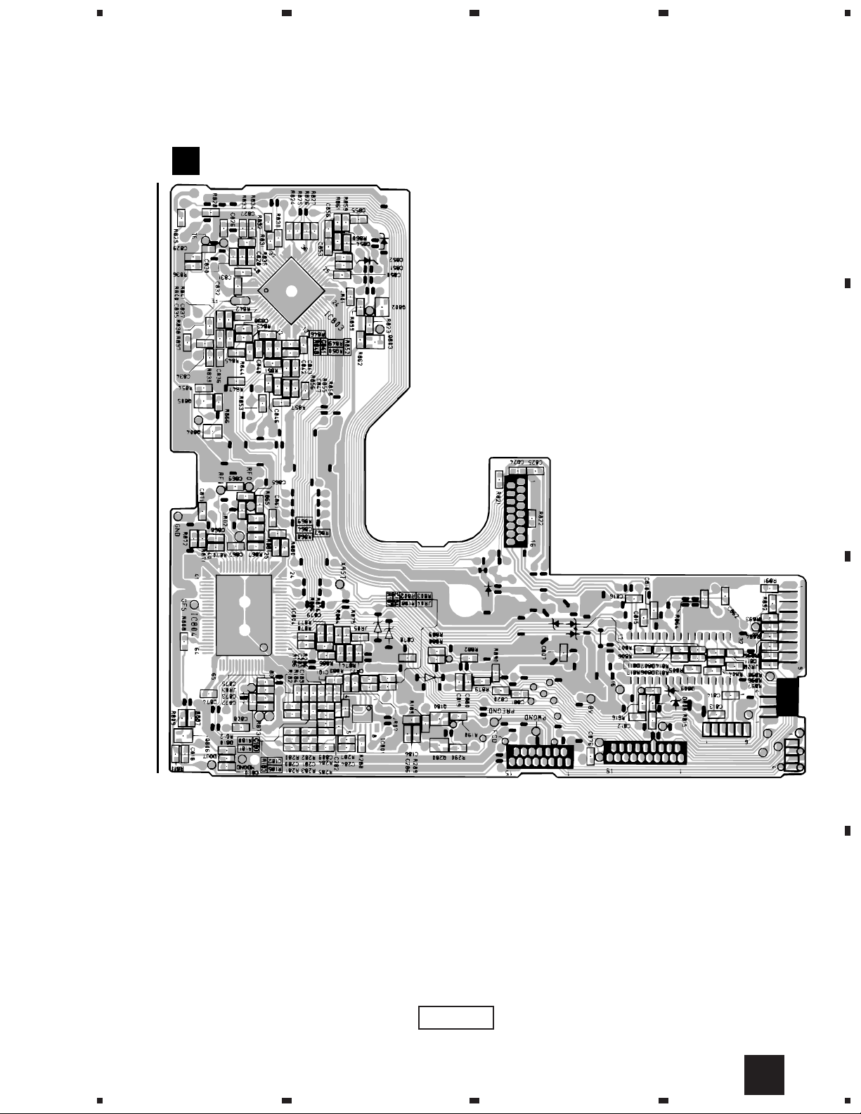
IC803
Q802
Q803
Q805
Q804
1
CD UNIT
C
234
X-MDX707, XR-C2MD
A
B
IC801
Q806
IC804
C
Q180
Q280
D
SIDE B
1
2
3
4
C
43
Page 44

1
X-MDX707, XR-C2MD
4.4 DECK UNIT
A
DECK UNIT
E
B
23
DECK
MECHANISM
4
C
F
CN453
Q320 Q322 Q323 Q309 Q308
Q319 Q325
Q321
Q106
Q107 Q316
Q207
Q315 Q206
Q318 IC305
Q317 Q104
IC304
Q208 Q305
Q204
IC301
Q103
Q203 Q202
Q301 Q304
Q108 Q303
Q314 Q101
Q313
VR301VR102VR202VR101VR201
Q306 Q312
Q307
Q311
Q324
Q302
Q102
IC302
Q201
DECK
MECHANISM
D
SIDE A
44
E
1234
Page 45

1
DECK UNIT
E
234
X-MDX707, XR-C2MD
A
B
C
D
SIDE B
E
1
2
3
4
45
Page 46
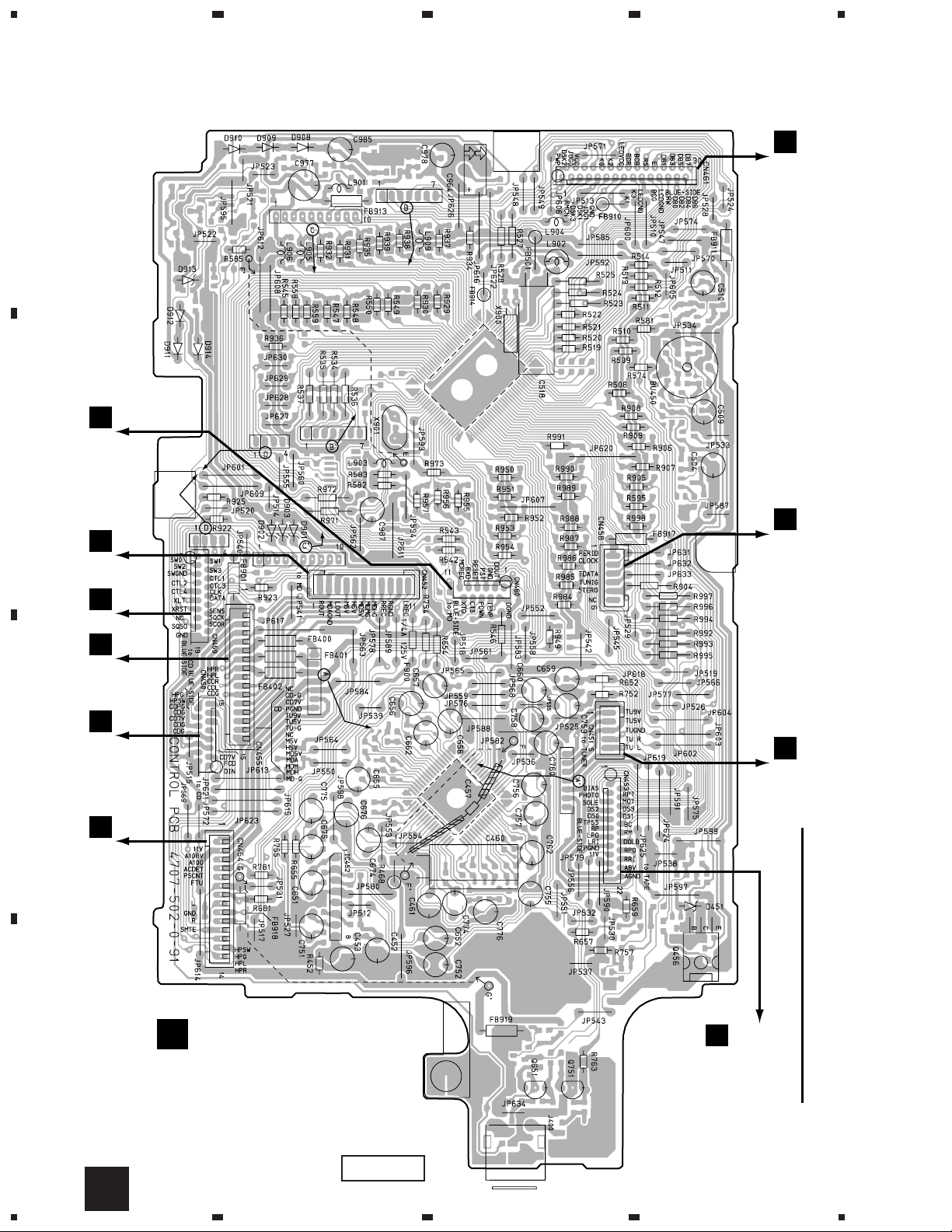
1
X-MDX707, XR-C2MD
4.5 CONTROL UNIT
A
D
CN504
B
23
4
I
CN700
C
D
CN503
C
CN802
G
CN400
CN406
C
CN801
G
CN401
CN405
A
WC2
A
WC1
IC452
Q456
CONTROL UNIT
F
D
E
CN302
Q651
Q751
SIDE A
46
F
1234
Page 47
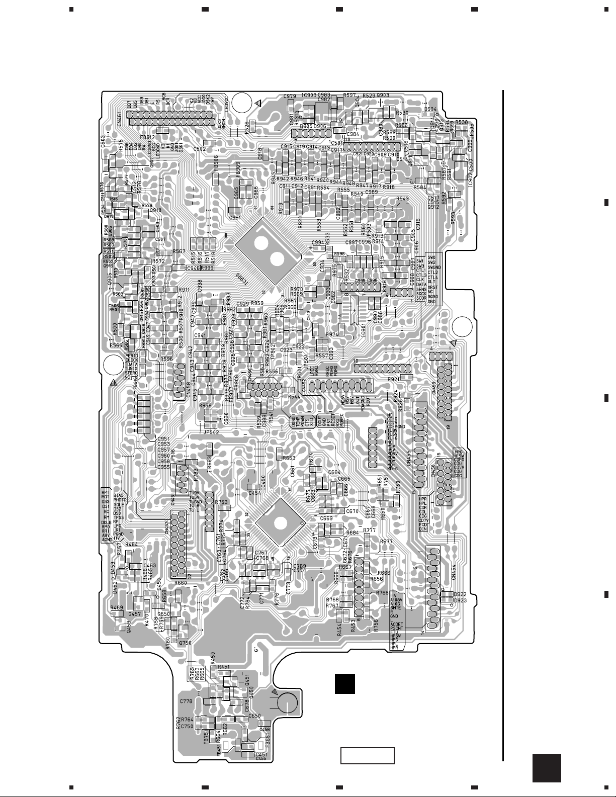
1
234
X-MDX707, XR-C2MD
IC903
Q907
Q917
Q910
Q906
Q909
Q916
IC900
Q905
Q915
Q908
Q903
Q914
Q913
Q911
IC902
Q912
IC901
A
B
C
IC450
Q457
Q459
Q650
Q750
CONTROL UNIT
F
Q451
Q450
D
SIDE B
F
1
2
3
4
47
Page 48

1
X-MDX707, XR-C2MD
23
4
4.6 AMP, PS UNIT
A
Q400
Q152
Q252
Q250
Q150
Q401
IC400
Q151
Q251
IC403
IC402
B
IC401
AMP UNIT
G
CN455
F
CN454
F
To
SPEAKER
IC
PCB
DI PCB
Q406
C
AC IN
D
48
G H
PS UNIT
H
SIDE A
1234
Page 49

AMP UNIT
G
1
234
X-MDX707, XR-C2MD
A
Q418
Q417
Q402
Q416
B
IC PCB
SIDE B
Q407
Q415
Q403
C
D
G
1
2
3
4
49
Page 50

1
X-MDX707, XR-C2MD
4.7 FRONT UNIT
A
F
CN461
B
FRONT UNIT
I
23
LCD PANEL
4
KEY
PCB
C
D
SIDE A
50
I
1234
Page 51

1
FRONT UNIT
I
234
X-MDX707, XR-C2MD
A
Q705
Q703
Q704
Q706
Q708
Q707
B
KEY PCB
Q702
Q700Q701
C
D
SIDE B
51
I
1
2
3
4
Page 52

1
X-MDX707, XR-C2MD
4.8 MD MOUNT
A
MD MOUNT
J
B
23
MD MECHANISM
4
IC122
IC122
Q103
Q105
C
IC201
Q105
Q103
D102
IC201
D
CN502
D
CN501
D
MD MECHANISM
SIDE A
52
J
1234
Page 53

IC101
Q101
1
MD MOUNT
J
234
X-MDX707, XR-C2MD
A
D101
Q101
IC101
IC152
Q162
Q163
IC181
IC125
Q104
Q102
IC103
IC121
Q181
IC171
Q182
IC123
IC202
IC181
IC152
D181
Q181
D183
Q182
IC123
IC121
B
Q162
Q163
Q104
Q102
IC125
IC103
IC171
C
IC202
R142
R123 R213
D
SIDE B
J
1
2
3
4
53
Page 54

X-MDX707, XR-C2MD
5. PCB PARTS LIST
NOTES:
Mark No. Description Part No. Mark No. Description Part No.
Parts marked by "NSP" are generally unavailable because they are not in our Master Spare Parts List.
The mark found on some component parts indicates the importance of the safety factor of the part.
Therefore, when replacing, be sure to use parts of identical designation.
When ordering resistors, first convert resistance values into code form as shown in the following examples.
Ex.1 When there are 2 effective digits (any digit apart from 0), such as 560 ohm and 47k ohm (tolerance is shown by J=5%,
and K=10%).
560
47k
0.5
1
56 x 10
47 x 103
R50
1R0
1
561
473
RD1/4PU J
RD1/4PU J
RN2H K
RS1P K
561
473
R50
1R0
Ex.2 When there are 3 effective digits (such as in high precision metal film resistors).
5.62k RN1/4PC F562 x 10
1
5621
5621
LIST OF ASSEMBLIES
TUNER UNIT 4707021000
CD UNIT 4707030000
MD UNIT 4707025000
DECK UNIT 4707015000
CONTROL UNIT 4707006000
AMP UNIT 4707001000
NSP IC PCB
NSP DI PCB
(Please order AMP UNIT for the necessity IC PCB and DI
PCB ASSEMBLIES. )
PS UNIT (LBWXJ TYPE) 4707014000
PS UNIT (NLWXJ/HK TYPE) 4707012000
FRONT UNIT 4707035000
NSP SW PCB
NSP HP PCB
(Please order FRONT UNIT for the necessity SW PCB and
HP PCB ASSEMBLIES. )
NSP MD MOUNT A-4917-020-A
PMS L-SW 1-668-261-11
D-SW MOUNT BOARD 1-668-262-11
TUNER UNIT
A
SEMICONDUCTORS
IC2 (TC9216P) 0911177300
IC1 (TA2099N) 0911209800
Q3 TRANSISTOR 0906222500
Q5, Q6 2SA933S
Q7-Q10, Q12 2SC1740S
Q1 (2SC1740SLN) 0906205318
Q11 2SC2786
Q4 DTC114TS
D2-D5 1SS133
COILS AND FILTERS
CF1, CF3 CERAMIC FILTER 0039067000
L4, L5 MPX FILTER 0039876000
L3 INDUCTOR LHL06TB221K 0991402215
L6 AXIAL INDUCTOR LAU221J
TRANSFORMER
T1 AM IFT-PCFAZH-AC015 0012340000
CAP ACITORS
C36 CCCCH150J50
C44 CCCCH270J50
C45 CCCCH330J50
C22 CCCSL680J50
C25 CEATR10M50
C1, C20, C49 CEAT100M50
C14, C42 CEAT101M10
C26, C55 CEAT1R0M50
C38 CEAT220M25
C52 CEAT221M16
C39 CEAT3R3M50
C31-C34, C13, C56 CEAT4R7M50
C27 CEATR47M50
C40 CGCYX103K25
C19, C28 CGCYX153K25
C21 CGCYX473K25
C24 CGCYX683K25
C6 CKCYF103Z50
C2, C3, C50 CKCYF223Z50
C46-C48 CKPUYB101K50
C5, C29, C30, C43, C53 CKPUYB102K50
C8, C15, C37, C51, C54 CKPUYF103Z25
C12, C18 CKPUYY103M16
RESISTORS
All Resistors RD1/4PU&&&J
OTHERS
AT1 ANTENNA TERMINAL 4P 003402900013
CF5 C FILTER,CDA10.7MG82 0039155000
RF2 AM RF TUNING UNIT 0039640000
RF1 RF MODULE,TFFJ4E 0039655000
WC1 WIRE CONNECTOR 5P 4701569000
WC2 WIRE CONNECTOR 6P 4701570000
304 CONNECTOR PLATE SP 1600779000
X1 CRYSTAL(4.5MHz) 0038168000
54
Page 55

X-MDX707, XR-C2MD
Mark No. Description Part No. Mark No. Description Part No.
HP PCB
B
HP PCB is included to FRONT UNIT.
SEMICONDUCTORS
D750, D751 1SS133
OTHERS
CN750 CONNECTOR PIN,5PIN 0034751005
J700 MINI JACK 3.5 003352100001
H/P PCB 4707525092
CD UNIT
C
SEMICONDUCTORS
IC803 (CXA1782BQ) 0911168502
IC802 (BA5936S) 0911209400
IC801 BA4510F
IC804 CXD2508AQ
Q801 (2SA966-Y) 0906209425
Q802-Q804 2SA1037K
Q805 2SC2412K
D801-D803 1SS133
D804, D805, D812 MTZJ5.1B
COIL
L801 LAU100J
C830 CKSQYB223K50
C836, C840, C850, C852 CKSQYB333K50
C832, C864, C881 CKSQYB473K50
C807-C810, C824, C825, C854, C867 CKSQYF104Z25
C874, C876 CKSQYF104Z25
RESISTORS
VR803 SEMI-FIXED VOLUME(10kΩ) 0031781103
VR801, VR804 0031781203
SEMI-FIXED VOLUME(20kΩ)
VR802 SEMI-FIXED VOLUME(50kΩ) 0031781503
R801 RD1/4PM470J
R857 CHIP RESISTER 9281572242
Other Resistors RS1/10S&&&J
OTHERS
WIRE CLAMPER 30 0034475000
CN801 CONNECTOR PIN,15PIN 0034887015
CN802 CONNECTOR PIN,19PIN 0034887019
CN803 CONNECTOR PIN,16PIN 0034887016
CN804 WIRE CONNECTOR 6P 4701571000
CN805 WIRE CONNECTOR 4P 4707563000
CN806 WIRE CONNECTOR 9P 4707564000
CN807 WIRE CONNECTOR 4P 4701568000
X801 CRYSTAL(16.1344MHz) 0038136000
CAPACITORS
C803 ELECT. CAPACITOR 0938913326
C800 CERAMIC CAPACITOR 9320240400
C838 CCSQCH101J50
C855 CCSQCH220J50
C872, C873 CCSQCH270J50
C819 CCSQCH330J50
C180, C280 CCSQCH471J50
C877-C879 CCSQCH560J50
C186, C286 CCSQCH681J50
C183, C184, C283, C284 CCSQCH820J50
C185, C285 CEAT100M50
C805, C806, C823 CEAT101M10
C822 CEAT1R0M50
C844 CEAT220M25
C802, C833, C848, C849, C866, C884 CEAT470M10
C839, C870 CEAT4R7M50
C845 CEATR10M50
C821 CEJA100M16
C801 CEJA101M10
C841, C847, C851, C853, C861, C868 CKSQYB103K50
C869, C871 CKSQYB103K50
C831, C835, C837 CKSQYB104K25
C181, C182, C281, C282 CKSQYB122K50
C829, C865 CKSQYB152K50
C834 CKSQYB222K50
MD UNIT
D
SEMICONDUCTORS
IC505 (BA10358) 0911110000
IC501 (S-81340HG-KJ-X) 0911209300
IC503 (PCM3003E-T2) 0911505000
IC504 BA4510F
IC502 TC7WU04FU
Q502 DTA114EK
Q501 DTC114EK
Q503, Q504 DTC114TK
D501-D504 1SS133
COILS
L510, L511 INDUCTOR 0991401005
L506-L508 LAU100J
CAPACITORS
C532, C533 CCSQCH130J50
C506, C519, C536 CEAT100M50
C504, C507, C509, C511 CEAT101M10
C501 CEAT102M10
C538, C539, C615, C616 CEAT1R0M50
C502 CEAT331M16
C522, C524, C525, C527, C529, C546 CEAT4R7M50
C547 CEAT4R7M50
C508, C510, C520, C526, C528, C534 CKSQYB104K25
C537 CKSQYB104K25
C544, C545, C548, C549 CKSQYB122K50
C542, C543 CKSQYB153K50
C540, C541 CKSQYB562K50
55
Page 56

X-MDX707, XR-C2MD
Mark No. Description Part No. Mark No. Description Part No.
RESISTORS
R650 RD1/4PM100J
Other Resistors RS1/10S&&&J
OTHERS
CN501 CONNECTOR 16P 0034688016
CN502 CONNECTOR 19P 0034688019
CN503 WIRE CONNECTOR 11P 4701572000
CN504 CONNECTOR PIN 11PIN 0034887011
EF501-EF512 0011612203
FMIFIL,DSS306-93B101M100
FB501, FB502, JP545, JP587, JP565 0011813000
FERRITE BEAD
FB550, FB553, FB508 CHIP BEAD DTF1067
R503, R504, R625, R626 CHIP BEAD DTF1067
WL030140040B1(WASHER) 0987100600
TH501 THERMISTOR 0918004400
X501 CRYSTAL 22.5792MHz 0038204000
SHIELD PLATE 4750735000
DECK UNIT
E
SEMICONDUCTORS
IC301 (TA8142AP) 0911166600
IC304 (CXA1552P) 0911200400
IC305 BA15218N
IC302 BA335
Q319 (2SA1359) 0900008725
Q306, Q311, Q321 (2SD467) 0906202003
Q304, Q307 (DTA114YS) 0906222500
Q106, Q206, Q108, Q208, Q312, Q313 2SC3330
Q314, Q324 2SC3330
Q107, Q207, Q302, Q303, Q308, Q309 2SD1302
Q317 2SD1302
Q101, Q102, Q201, Q202 2SJ103
Q103, Q104, Q203, Q204, Q301, Q305 DTC114TS
Q315, Q316, Q318, Q320, Q322, Q323 DTC114TS
Q325 DTC114TS
D307 (DRA-1T4) 0915033250
D303, D304 (DRA-RB721Q) 0915037750
D101, D201, D301, D305 1SS133
D308, D309 MTZJ5.1B
D306 MTZJ7.5B
COILS
L103, L203 INDUCTOR 9P562J-R 0990415624
L301 LAU100J
L302 INDUCTOR 0991401005
TRANSFORMER
T301 OSC TRANS-10 0015083000
CAPACITORS
C103, C107, C111, C203, C207, C211 CCSQCH101J50
C312, C334 CEAT100M50
C314, C325, C331 CEAT101M10
C332 CEAT101M25
C101, C108, C120, C201, C208, C220 CEAT1R0M50
C112, C212, C323, C324, C330 CEAT220M25
C322 CEAT221M10
C125, C225, C318 CEAT2R2M50
C105, C205, C317, C326, C342, C304 CEAT470M10
C305 CEAT470M10
C319, C335 CEAT471M10
C126, C226, C301, C123, C223 CEAT4R7M50
C313 CEATR47M50
C102, C202 CGCYX102K25
C106, C206 CGCYX223K25
C113, C121, C213, C221, C328 CKSQYB102K50
C306, C307 CKSQYB103K50
C344 CKSQYB104K50
C127, C227 CKSQYB183K50
C327 CKSQYB333K50
C128, C228 CKSQYB392K50
C104, C110, C119, C124, C204, C210 CKSQYF105Z16
C219, C224, C308, C311, C315, C316 CKSQYF105Z16
C333, C336, C343 CKSQYF105Z16
C329 CQMA102J50
C122, C222 CQMA104J50
C116, C216 CQMA183J50
C303 CQMA222J50
C302 CQMA562J50
RESISTORS
VR101, VR102, VR201, VR202, VR3010031781103
SEMI-FIXED VOLUME(10KΩ)
R368 RD1/4PM101J
R348 RD1/4PM471J
R124, R314, R334 RD1/4PU102J
R377 RD1/4PU222J
R124, R314, R334 RD1/4PU102J
R311, R372, R310 RD1/4PU103J
R127 RD1/4PU152J
R320 RD1/4PU153J
R318, R322, R338, R345, R362 RD1/4PU221J
R216, R317 RD1/4PU223J
R346 RD1/4PU561J
Other Resistors RS1/10S&&&J
OTHERS
CN301 WIRE CONNECTOR 6P 4701563000
CN302 CONNECTOR 22P 0034688022
CN303 CONNECTOR 9P,SBRK 0034208009
CN304 CONNECTOR 5P,BTMK 0034209005
CN305 CONNECTOR 3P,IMSA-91 0034210003
56
Page 57

X-MDX707, XR-C2MD
Mark No. Description Part No. Mark No. Description Part No.
CONTROL UNIT
F
SEMICONDUCTORS
IC900 (CXP740096-109Q) 0037502200
IC903 (S-81350HG-KD-T1) 0911186600
IC902 (S-80727AN-DQ-T1) 0911851600
IC452 BA15218N
IC450 LC75394NED
IC901 TC74HCT08AF
Q456 (2SA1359Y) 0900008725
Q459, Q650, Q750, Q905-Q907 0906505419
Q915-Q917 (2SD1757K) 0906505419
Q904 2SA1037K
Q451, Q457, Q903, Q908-Q914 2SC2412K
Q651, Q751 2SD1302
Q450 DTA114TK
D908-D912 (DRA-1T4) 0915033250
D450, D452, D453, D904-D906, D922 1SS355
D923 1SS355
D901-D903, D914 MTZJ5.1B
D451 MTZJ5.6B
COILS
L901, L903-L906, L909 LAU100J
L902 INDUCTOR 0991401005
CAPACITORS
C964 (DX-5R5V224 0.22µF/5.5V) 0939932500
C514, C515, C673, C773, C905-C908 CCSQCH101J50
C913, C995-C998 CCSQCH101J50
C933, C934 CCSQCH150J50
C965, C966 CCSQCH270J50
C661, C761 CCSQCH330J50
C660, C662, C760,C762 CEATR10M50
C674, C774 CEAT100M50
C452, C453, C461, C676, C776 CEAT101M10
C652, C657-C659,C752, C757-C759 CEAT1R0M50
C518 CEAT102M6R3
C460 CEAT222M10
C656, C756, C985, C987 CEAT470M16
C675, C775, C655, C755 CEAT4R7M50
C651, C751 CEJA1R0M50
C671, C678, C771, C778 CKSQYB222K50
C665, C765 CKSQYB223K50
C667, C767 CKSQYB272K50
C670, C770 CKSQYB391K50
C666, C766 CKSQYB472K50
C668, C768 CKSQYB681K50
C664, C764 CKSQYB683K25
RESISTORS
R508-R514, R527, R528, R534-R537 RD1/4PU102J
R545, R550, R558, R574, R581, R583 RD1/4PU102J
R595, R929, R930-R935, R937-R939 RD1/4PU102J
R949-R951, R953, R955, R957, R971 RD1/4PU102J
R972, R985-R998 RD1/4PU102J
R652, R752 RD1/4PU103J
R582, R585, R973 RD1/4PU104J
R547-R549, R559 RD1/4PU332J
R905-R909, R519-R525, R659, R763 RD1/4PU472J
R654, R754 RD1/4PU123J
R681, R781 RD1/4PU132J
R657, R757 RD1/4PU822J
R655, R755 RD1/4PU222J
Other Resistors RS1/10S&&&J
OTHERS
CN450 CONNECTOR 15P 0034221015
CN451 CONNECTOR PIN,5PIN 0034750005
CN452 CONNECTOR PIN,11PIN 0034750011
CN453 CONNECTOR 22P 0034203022
CN454 WIRE CONNECTOR 14P 4707561000
CN455 WIRE CONNECTOR 15P 4707562000
CN458 CONNECTOR PIN,6PIN 0034750006
CN459 CONNECTOR 19P 0034203019
CN460 CONNECTOR 11P 0034221011
CN461 CONNECTOR 30P 0034203030
X900 CRYSTAL 32.768kHz 0038201000
X901 CRYSTAL 16.00MHz 0038202000
R468, FB400, FB901, FB910, FB911 0011813000
FB501, FB914, FB917-FB919 0011813000
FERRITE BEAD
FB906-FB908, FB915, FB916 DTF1067
EMI BEAD BK2125HS601
C504, C509, C510 CEJA220M16
C977, C978 CEJA221M6R3
C457 CKPUYF104Z50
C454, C650, C750, C982, C455 CKSQYB102K50
C962, C981 CKSQYB104K16
C463, C500, C502, C503, C505-C508 CKSQYB105K10
C511, C512, C961, C979, C980, C983 CKSQYB105K10
C984, C993, C994, C999, C519 CKSQYB105K10
C669, C769 CKSQYB152K50
C663, C763 CKSQYB224K16
BU450 SPEAKER PIEZO CB13PA 002384700013
J400 PIN JACK 2P 003402700013
WIRE CONNECTOR 4P 4707571000
WIRE CONNECTOR 7P 4707572000
WIRE CONNECTOR 7P 4707573000
WIRE CONNECTOR 10P 4707574000
F900 FUSE PI-251.250 004560704102
CONTROL PCB 4707502091
57
Page 58

X-MDX707, XR-C2MD
Mark No. Description Part No. Mark No. Description Part No.
AMP UNIT
G
SEMICONDUCTORS
IC401 (LA4663) 0911209600
IC402, IC403 (PQ20RX11) 0911209700
IC400 BA15218N
Q406 (2SA1359) 0900008725
Q400 (2SD467) 0906202003
Q401 (2SA966) 0906209425
Q402, Q403, Q407, Q415-Q417 2SC2412K
Q150, Q152, Q250, Q252 2SD1302
Q418 DTA114TK
D423 DR KBU603 0913013600
D404, D422 (DRA-1T4) 0915033250
D424-D427 (1N5401TM) 2626323000
D401, D405, D408, D416-D418 1SS355
D421 MTZJ4.7B
D406 MTZJ5.1B
D400, D402 MTZJ5.6B
D403 MTZJ6.8B
CAPACITORS
C432, C433, C436, C437 CAPACITOR 0939934300
C157, C257 CCSQCH100D50
C435 CEAT100M50
C252 CEAT101M10
C406 CEAT101M16
C400, C411 CEAT102M10
C154, C254, C426, C440 CEAT1R0M50
C152, 158, C258, C424, C403 CEAT221M10
C412 CEAT221M16
C167, C168, C267, C268 CEAT222M25
OTHERS
CN401, CN406 0034751006
CONNECTOR PIN 6PIN
CN400 CONNECTOR PIN 7PIN 0034751007
CN405 CONNECTOR PIN 8PIN 0034751008
CN402 SPEAKER TERMINAL 4P 003402600013
CN403 CONNECTOR PIN 5PIN 0034888005
BAR LOCK CABLE TIE 0064631050
HEAT SINK 4707720000
GI-HG3E1.0*5 0955201005
SCREW P3*10-SN 0971030101
WC401, WC403 4701576000
WIRE CONNECTOR 4P
IC PCB 4707500092
DI PCB 4707500093
PS UNIT
H
Although 4707014000 and 4707012000 are different in part number ,
they have the same servise parts.
FILTER
LF601 LINE FILTER COIL LF2 0013914000
CAPACITORS
SK601 SPARK KILLER 003994600011
OTHERS
PIN TERMINAL 0034473000
FUSE HOLDER 0045522000
COVER,SPARK KILLER 0064644000
PT6AWG03T20 0950103020
WC601 WIRE CONNECTOR 5P 4701565000
C402, C415, C417 CEAT470M16
C428, C434 CEAT472M16
C429 CEAT472M25
C155, C255, C431 CEAT4R7M50
C407, C427 CEHAT470M16
C160-C163, C260-C263 CFTYA274J50
C156, 159, C256, C259, C410 CKSQYB102K50
C401, C404, C409 CKSQYB103K50
C405, C413, C414, C416, C419, C425 CKSQYB105K10
C151, C251, C439 CKSQYB105K10
C420, C438 CKSQYF105Z16
RESISTORS
R162, R163, R262, R263 RD1/4PM2R2J
R415 RD1/4PU102J
R164, R165, R264, R265, R403, R425 RD1/4PU103J
R433 RD1/4PU103J
R400 RD1/4PU331J
R153, R253 RD1/4PU472J
R168, R268, R437 RD1/4PU473J
Other Resistors RS1/10S&&&J
PS PCB 4707510091
FRONT UNIT
I
SEMICONDUCTORS
Q700-Q702 2SC2412K
Q703-Q708 (2SD1963-S) 0906505319
D701-D706 LD SLP-7118C-51H-S 0916038600
LD701, LD702 LD NSTM515S 0916039600
D718, D719 1SS355
D712-D717 UDZS5.1B
SWITCHES
S700-S719, S721, S722 0028650000
TACT SWITCH
S723 TACT SWITCH 002871200001
CAP ACITORS
C741, C742 CKSQYB103K50
C700-C702, C738-C740 CKSQYB105K10
58
Page 59

X-MDX707, XR-C2MD
Mark No. Description Part No. Mark No. Description Part No.
RESISTORS
R748-R751, R754-R757, R766, R767 9281575612
R771, R772 9281575612
R752, R753, R758, R759, R768-R770 9281576812
R773-R775 9281576812
R706, R707, R709, R710 RD1/4PU103J
R711, R712 RD1/4PU331J
Other Resistors RS1/10S&&&J
OTHERS
FB701, FB702 CHIP BEAD DTF1067
CN700 CONNECTOR PIN 30P 0034887030
LD700 CONNECTOR 14P 0034689014
EN700 ROTARY ENCODER EC12E24 0031936000
RM700 REMOCON REC,SPS-444-1 0039648000
LC700 LCD PANEL LMG172C1-MFPT 004044100021
LCD HOLDER 4707270000
LCD LENS 4707271000
DIFFUSION PLATE 4707274000
JW700 WIRE CONNECTOR 2P 4707570000
REFLECTOR L 4707877000
REFLECTOR R 4707878000
DOUBLE FACE A 4701887000
DOUBLE FACE B 4701888000
CUSHION(FRONT) 4701896000
DIFFUSION SHEET 4707890000
FRONT PCB 4707525091
SW PCB 4707525093
CAPACITORS
C142 CCSQCH101J50
C106 CCSQCH102J50
C205 CCSQCH150J50
C105 CKSQYB103K50
C117 CKSQYB104K25
C131 CKSQYB153K50
C116 CKSQYB223K50
C115 CKSQYB224K16
C189 CKSQYB333K25
C112 CKSQYB472K50
C132 CKSQYB474K16
C158 CKSQYB682K50
C111 CKSQYB683K25
C107 CKSQYF104Z25
C113 CKSYB105K16
C CKSYB152K50
C CHIP TANTALUM ELECT 1-104-851-11
C184 CHIP ELECT 22mF 1-107-836-11
C151 CHIP ELECT 100mF 1-126-206-11
RESISTORS
R169 SQUARE CHIP 1W 1-217-806-11
R163 METAL FILM 1.0W 1-219-724-11
R213 CHIP NETWORK 10KW 1-236-908-11
R120 CHIP NETWORK 100W 1-233-576-11
R204 NETWORK 100KW 1-233-810-21
R166 SQA TYPE CHIP 2.2W 1-240-032-11
Other Resistors RS1/10S&&&J
MD MOUNT (Reference Information)
J
SEMICONDUCTORS
IC122 TC7S08F
IC123 TC7WU04F
IC101 (CXA2523AR) 8-752-080-95
IC121 (CXD2652AR) 8-752-384-47
IC202 (LB1638MTE-L) 8-759-823-87
IC125 (MSM51V4400-70TSK) 8-759-498-44
IC152 (BH6511FS-E2) 8-759-430-26
IC171 (BR24C01AF-E2) 8-759-484-73
IC181 (TC74ACT540FT(EL)) 8-759-523-48
IC201 (RU8X12MF-0023) 8-759-533-77
Q101,Q163 DTA144EK
Q103,Q104 DTC114EK
Q102 2SA1037K
Q182 (2SK1764KYR) 8-729-017-65
Q181 (2SJ278MYTR) 8-729-018-75
Q162 (2SB798-T1DK) AZQ7132
IC103 (FMW1-T-148) 8-729-903-10
D181,D183 (F1J6TP) 8-719-046-87
D101 CHIP DIODE ARRAY DAN202K
COILS
L101 FERRITE BEED INDUCTOR 1-414-233-21
L FERRITE BEED INDUCTOR 1-414-235-11
L CHIP CONDUCTOR(2012) AZC7283
OTHERS
CN101 FFC/FPC CONNECTOR 21P 1-691-385-21
CN106 FFC/FPC CONNECTOR 6P 1-766-336-21
CN103 FFC/FPC CONNECTOR 16P 1-770-425-11
CN110 CONNECTOR PIN 5P 1-774-731-21
CN104 FFC/FPC CONNECTOR 4P 1-778-283-11
CN102 FFC/FPC CONNECTOR 19P 1-778-460-11
CN105 FFC/FPC CONNECTOR 7P 1-779-345-11
X202 SERAMIC RESONETOR 1-760-174-31
(32.768kHz)
X201 XTAL RESONETOR (12MHz) 1-760-872-11
L-SW MOUNT BOARD
OTHERS
FFC/FPC CONNECTOR 6P 1-766-336-21
PUSH SWITCH(1KEY) 1-771-092-21
PUSH REVER SW(1KEY) 1-771-326-11
D-SW MOUNT BOARD
OTHERS
2PIN PUSH SW(2KEY) 1-771-327-11
FFC/FPC CONNECTOR 7P 1-779-345-11
59
Page 60

X-MDX707, XR-C2MD
6. ADJUSTMENT
6.1 CASSETTE DECK SECTION
Adjustment points and test points are shown in Fig.4 and Fig.6.
•
Adjustment
The test tape is played. And, for the shape of waves of the test point (CN304 PB Lch and PB Rch) to become, for part A to become the
maximum, and to minimize part B, the adjustment screw for azimuth is adjusted.
Both FORWARD and REVERS are adjusted. Do the screw lock to two places after the adjustment ends.
B
Oscilloscope
(X-Y Mode)
A
Top View
DECK UNIT
CN304
PB L ch
PB R ch
Adjustment Screw
FORWARD Side REVERS Side
Fig. 1 Adjustment Points
Mechanical Adjustment
Test tape: NCT-111 (3kHz, 30min).
•
Tape Speed Adjustment
No. Mode Test Tape Adjusting Points Measurement Points Adjustment Value Remarks
PLAY1
NCT-111 (Playback: 3 kHz)
adjustment screw
JA501
Head Phone Jack
3000 Hz ± 90Hz
60
Plastic Driver
Adjustment Screw
Motor
Fig. 2
Page 61
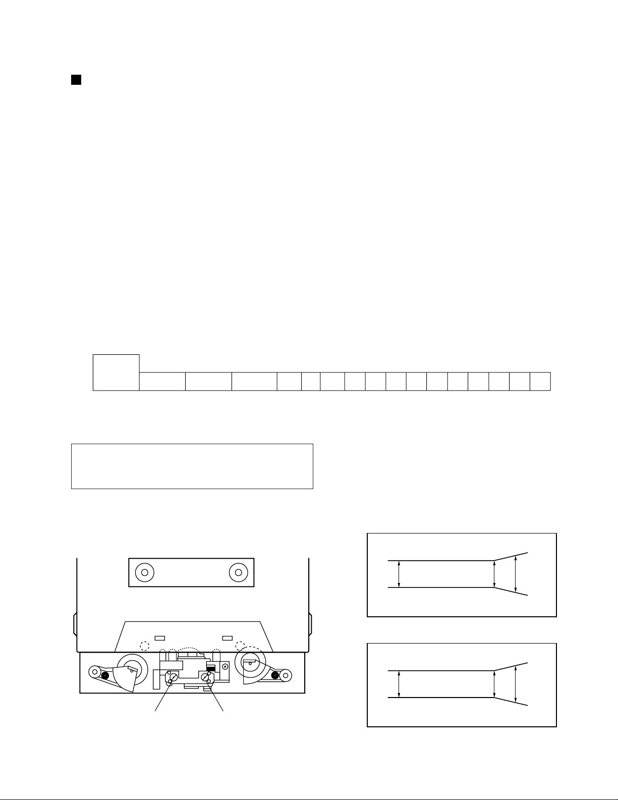
Electrical Adjustment
Check the following before starting.
(1) Confirm that the tape speed adjustment has been completed.
(2) Clean the heads and demagnetize them using a head eraser.
(3) Set the measurement level to 0 dBV = 1 Vrms.
(4) Use the specified tape for adjustment. Use the labeled (A)
side of the test tape.
STD-331E : For playback check
STD-632 : Normal blank tape
(5) Provide yourself with the following measuring devides:
AC millivoltmeter
•
Low-frequency oscillator
•
Attenuator
•
Oscilloscope
•
(6) Adjust both right and left channels unless otherwise specified.
(7) Turn the DOLBY NR switch off unless otherwize specified.
(8) Warm up the unit for several minutes before adjustment.
In particular, be sure to warm up the unit in the REC/PLAY
mode for 3 to 5 minutes before starting recording/playback
frequency characteristics adjustment.
(9) Always follow the indicated adjustment order.
Otherwise, a complete adjustment may not be achieved.
X-MDX707, XR-C2MD
Playback Adjustment
(1) Head Azimuth Adjustment
(2) Playback Level Adjustment
Recording Adjustment
(1) Recording Bias Adjustment
(2) Recording Level Adjustment.
(3) ALC Operation Check
* When the tape is played with both of side panel L and R removed
(state that reception front is floating from ground). when adjusting ,
the noise might be superimposed.
In this case, the front chassis must short circuit to the CD mechanism
cover in the lead wire.
0 dB
30s
315 Hz
0 dB: 315 Hz, 250 nwb/m
30 s 30 s 30 s 10s 10s .......................................................................................................... 10s
6.3 kHz 10 kHz 315 Hz 14 kHz
Fig. 3 NCT-132X Test Tape
Dolby noise reduction manufactured under license from Dolby
Laboratories Licensing Corporation.
“DOLBY” and the double-D symbol are trademarks of Dolby
Laboratories Licensing Corporation.
12.5
kHz
10 kHz
8 kHz 4 kHz 2 kHz
6.3
kHz
PLAY BACK
250
3dB
RECORDING
1 kHz
500Hz250Hz125
Hz
10k
3dB 4dB
63 Hz 40 Hz
–20 dB
12.5k
FWD Azimuth Adjustment Screw REV Azimuth Adjustment Screw
Fig. 4 Head Azimuth Adjustment
250
3dB
10k
3dB 5dB
12.5k
Fig. 5 Frequency Characteristics
61
Page 62

X-MDX707, XR-C2MD
Playback Adjustment
(1) Head Azimuth Adjustment
Do not switch between forward and reverse operation with the screwdriver inserted.
•
Step Mode Input Signal/ Test Tape Adjusting Points
PLAY1
NCT-132X test tape
(Playback: 10kHz, -20dB)
Head azimuth adjustment
screw (Fig. 4)
(2) Playback Level Adjustment
Since this adjustment determines playback Dolby NR level, perform it carefully.
•
Step Mode Input Signal/ Test Tape Adjusting Points
PLAY1
NCT-132X test tape
(Playback: 315Hz,0dB)
L ch
R ch
VR101
VR201
Measurement Adjustment
Points Value
CN304 PB L ch
Measurement Adjustment
Points Value
CN304 PB L ch
PB R ch
PB R ch
Max. playback
signal level
-8.2 dBV
Remarks
After adjustment, apply
silicon bond to the head
azimuth adjustment screw.
Remarks
Recording Adjustment
(1) Recording Bias Adjustment
Step Mode Input Signal/ Test Tape Adjusting Points
REC
1
Since this adjustment affects recording bias, prevent distortion from increasing due to underbias.
•
Load the STD-632 test tape and
set the recording mode.
VR301
(2) Recording Level Adjustment
Step Mode Input Signal/ Test Tape Adjusting Points
Input a 400Hz signal to the AUX
1
REC
REC=
2
PLAY
terminal and set the input
selector to AUX.
Load the STD-632 test tape and
record/playback the 400Hz signal.
125mV is input.
L ch
R ch
VR102
VR202
(3) ALC Operation Check
Step Mode Input Signal/ Test Tape Adjusting Points
1
REC
2
Load the STD-632 test tape and
input a 315Hz signal to the AUX
terminal and set the input selector
to AUX.
400mV is input.
The input level of
procedure 1 is set and the
level is set to 1.25V.
Measurement Adjustment
Points Value
CN305
REC BIAS
Measurement Adjustment
Points Value
REC L ch
CN304
CN304 PB L ch
CN304 REC L ch
REC R ch
PB L ch
PB R ch
PB R ch
Measurement Adjustment
Points Value
REC R ch
Remarks
13.5V ± 0.5V
Remarks
-22.5 ± 1dB
-18.4 ± 1dB
Repeat recording, playback and adjustment
until playback level of the 400Hz signal
becomes -18.4dBV ± 1.0dB.
Remarks
-12.2 ± 1.0dBV
-9.7 ± 1.5dBV
62
Page 63

X-MDX707, XR-C2MD
DECK UNIT
VR201
(PB R ch)
VR101
(PB L ch)
VR202
(REC R ch)
VR102
(REC L ch)
GND
11V
DECK SW3
IC304
IC301
PB L ch
PB R ch
GND
REC R ch
REC L ch
REC Lch IN
CN304
IC305
GND
GND
REC BIAS
CN303
CN305
VR301
(REC BIAS)
SIDE A
DECK UNIT
PRI GND
GND
DECK SW1
REC R
REC F
PHOTO
HALF
SOLENOID
MECHA +B
BIAS CONT
BIAS GND
BIAS
SOLENOID
MODE
DECK SW0
REC/MUTE
BIAS OUT
REC/PLAY
BIAS GND
DECK SW2
HEAD GND
REC BIAS
PB R ch OUT
PB L ch OUT
PRI GND
REC L ch
REC R ch
GND
HEAD L ch
HEAD R ch
Fig. 6 Adjustment Points
DOLBY
ON/OFF
GND
VCC
REPEAT
TPSS
SIDE B
63
Page 64

X-MDX707, XR-C2MD
6.2 MD SECTION
Because material was not able to be acquired when the service manual is made, the adjustment of MD is not published.
6.3 CD SECTION
CD UNIT is taken out according to the procedure of DISASSEMBLY. And, please adjust the part CD after connecting connectors.
6.3.1 PREPARATIONS
(1) Jigs and Measuring Instruments
CD TEST DISC
(YEDS-7)
screwdriver
(large)
(2) Necessary Adjustment Points
When
Exchange
PICKUP
Precise
screwdriver
Low-frequency
oscillator
Adjustment Points
1.2.3.4
screwdriver
(small)
Dual-trace
oscilloscope
(10 : 1 probe)
Page66-67
screwdriver
(medium)
Exchange
CD UNIT
Exchange
SERVO MECH ASSY
64
1.2.3.4
1.2.3.4
Page66-67
Page66-67
Page 65

6.3.2 Adjustment
(1) Adjustment Locations
X-MDX707, XR-C2MD
CN806
CN805
CN804
CN807
IC802
CN802
CN803
CN801
(FOCUS OFFSET)
VR801
VR802
(TRACKING BALANCE)
VR804
(TRACKING GAIN)
VR803
(FOCUS GAIN)
CD UNIT
SIDE A
TP1 (VC)
TP3 (TEO)
TP2 (RFO)
GND
GFS
DOUT
TE
VC
RFI
FE
RFO
IC804
MDGND
IC803
XRST
IC801
CD UNIT
PREGND
FCD
FO
TO
PWGND
8V
TP5 (TO)
TP4 (FO)
16
SIDE B
Fig. 7 Adjustment Locations
65
Page 66

X-MDX707, XR-C2MD
(2) Check and Adjustment
1. Focus Offset Adjustment
FUNCTION : CD
TEST DISC
NG
>1.0Vp-p
PLAY
START
TP2(RFO)
TP1(VC)
1
4
CD UNIT
2. Focus Gain Adjustment
FUNCTION : CD
Player
VR801
Focus Offset
Probe(10:1)
Eye pattern
OK(Smooth)
Oscilloscope
AC Mode
V : 20mV/div
H : 200nSec/div
GND
0.15~0.25Vp-p
66
TEST DISC
START
TP4(FO)
TP1(VC)
R=35m
PLAY
1
1
4
CD UNIT
0V
(VC)
VR803
Focus Gain
Oscilloscope
DC Mode
X : 20mV/div
H : 5mSec/div
Player
Probe(10:1)
GND
Page 67

3. Tracking Gain Adjustment
X-MDX707, XR-C2MD
FUNCTION : CD
TEST DISC
PLAY
VR804
(Tracking Gain)
START
TP5(TO)
TP1(VC)
1
4
CD UNIT
Player
4. Tracking Error Balance Adjustment
0.4~0.5Vp-p
0V
(VC)
Oscilloscope
DC Mode
V : 20mV/div
H : 5mSec/div
Probe(10:1)
GND
FUNCTION : CD
Keeps pushing
the FF button.
TEST DISC
START
TP3(TEO)
TP1(VC)
R=35mm
PLAY
2
4
CD UNIT
Tracking Offset
VC is made a center.
A : B symmetry ADJ
Player
VR802
Probe(10:1)
A=B
A
B
If not repair
0V
(VC)
Oscilloscope
DC Mode
V : 50mV/div
H : 5mSec/div
GND
67
Page 68

X-MDX707, XR-C2MD
7. GENERAL INFORMATION
7.1 DIAGNOSIS
7.1.1 TROUBLESHOOTING
CD troubleshooting
Please make the products to the power switching on
and the CD mode.
Is "CD DISC & NO DISC"
displayed after "CD DISC & TOC READING"
is displayed on the LCD display,
and is the same operation repeated
three times?.
YES
Please push CD OPEN/CLOSE KEY (1 or 2 or 3),
do the CD tray in OPEN, and put CD,
push CD OPEN/CLOSE KEY (1 or 2 or 3)
of DISC No. by which CD is put again,
and close the CD tray.
Are the number of total tracks
and playing time displayed?.
YES
Please push CD PLAY/PAUSE KEY
or CD SELECT KEY of DISC No..
NO
NO
1
2
Is the audio signal (analog)
being sent to the output jack?.
YES
Please push 4 KEY or ¢ KEY.
Can you smoothly
select music?.
YES
Please record from CD to MD.
Is the audio signal (digital)
being sent to the output jack?.
YES
OK
NO
NO
NO
3
4
5
68
Page 69

X-MDX707, XR-C2MD
1. "CD DISC & NO DISC" is displayed after "CD DISC & TOC READING" is displayed
on the LCD display and when the same operation do not repeat three times.
1
Is the power supply of
+7.8V (10 and 11 pins of CN801 )
supplied?.
YES
Do 38 pins (RESET) of IC901
show the wave forms of
Figure 1?.
YES
Does the clock pulse of 16MHz
appear to 39 pins (EXTAL) of IC901?.
(X901)
YES
Are 4.7V supplied to
F.CD (13 pins of CN801)?.
NO
NO
NO
NO
IC902 or IC402 is broken.
Please check the circuit of IC902 or IC402
in the surrounding.
IC903 is broken.
Please check the circuit of IC903 in the
surrounding.
Crystal (X901) is broken.
IC901 is broken.
Please check the circuit of X901 and IC901
in the surrounding.
IC901 is broken.
Please check the circuit of IC901
(76, 36, 35 pins) in the surrounding.
YES
Is the power supply of
+5V (11 pins of IC802)
supplied?.
YES
Please check IC802 and Q801.
Please check the circuit of IC802 in the
surrounding.
NO
IC802 or Q801 is broken.
Please check the circuit of IC802 or Q801
in the surrounding.
Fig. 1
69
Page 70

X-MDX707, XR-C2MD
2. When neither the number of total tracks nor the playing time are displayed.
2
How many seconds will it take by the time "NO DISC" is displayed
from the chuckingclamp of DISC that SELECT is done,
and doing the surroundings detection
(LMTSW (5 pins of CN804); Active "L") in Pick-up to the display?.
About 7 seconds
Please look at A.
About 12 seconds
Please look at B.
70
Page 71

2-A
X-MDX707, XR-C2MD
A
Fig. 2
Fig. 3
Is the laser normally radiated?.
Caution :
YES
Is the lens vertical motion ?.
Please confirm the radiation power
with the optical power meter.
YES
Please turn on the disk, close the CD tray,
and check the following.
Is the wave forms
of Figure 2 shown with 31 pins
(RFO) of IC803?.
YES
Is the wave forms
of Figure 3 shown with 25 pins
(FOK) of IC803?.
YES
NO
NO
Please check FFC wire connector
(CN803) from pick-up.
IC802 IC803 Confirmation with solder
NO
of IC804.
IC803 is broken.
Pick-up is broken.
25 of IC803 26 Confirmation with solder
NO
of 27 pins.
IC803 is broken.
A1
A2
Fig. 4
Fig. 5
Is the wave forms
of Figure 4 shown with 1 pin
(FEO) of IC803?.
YES
Is the wave forms
of Figure 5 shown with 2 pins
(FEI) of IC803?.
YES
Please check
IC803 surrounding circuit and IC803.
NO
IC803 is broken.
Please check the circuit of
1 and 2 pins of IC803 in the surrounding.
NO
Readjustment of focus gain (VR803).
(Refer to the CD adjustment).
71
Page 72

X-MDX707, XR-C2MD
2-A1. (The laser does not radiate.)
A1
Is base of Q802
description 5.0V?.
YES
Are when playing,
33 pins of IC803
2.8V or more?.
YES
Please check the circuit
of Q801 in the surrounding.
Please check FFC connector (CN803).
Q801 is broken.
Picking up is broken.
2-A2. (Is the lens vertical motion.)
A2
NO
NO
Please check 22 pins of IC804 and Q801,
and confirm solder.
Please check the circuit of IC803 of 33 pins
in the surrounding.
Please check a digital signal
of 19, 20 and 21 pins of IC803.
72
of Figure 6 shown with 13 pins and
Is the wave forms
16 pins of CN803?.
YES
Please check the FFC connector
from pick-up.
Pick-up is broken.
NO
Fig. 6 Fig. 7
Is the wave forms
of Figure 7 shown with 6 pins
(FEO) of IC803?.
YES
Please check the circuit of IC803
in the surrounding.
IC803 is broken.
NO
Please check the circuit in the
surrounding with the solder of
IC803 of 17 pins.
IC803 is broken.
IC804 is broken.
Page 73

X-MDX707, XR-C2MD
2-B
B
Please confirm the wave forms of IC803
of 31 pins (RFO) with the oscilloscope.
wave form wave form
Is the wave forms
of Figure 8 shown with 36 pins
(RF) of IC804?.
YES
Are 27 pins (LOCK) of IC804
in the state of "H"?.
YES
Please check 29, 30 and 31 pins of IC804.
Please check 27 and 30 pins of IC804.
IC804 is broken.
NO
NO
Is 16.93MHz shown
in 73 pins (X'TAL) of IC804?.
YES
Please check X 'TAL
and the circumference circuit.
IC804 is broken.
C
Please check the circuit of 36 pins
(RF) of IC804 and C869
in the surrounding.
IC804 is broken.
NO
Please check the circuit in the
surrounding with the solder of IC804.
IC804 is broken.
Fig. 8
73
Page 74

X-MDX707, XR-C2MD
2-C
C
Is the wave forms
of Figure 9 shown in 42 pins
(TEO) of IC803?.
YES
Is the wave forms
of Figure 10 shown in 44 pins
(TEI) of IC803?.
YES
Is the wave forms
of figure 11 shown in 13 pins
(TAO) of IC803?.
YES
Is the wave forms
of Figure 12 shown in 15 pins
and 16 pins of IC802?.
NO
NO
NO
NO
Please check FFC connector CN803.
IC803 is broken.
Please check the circuit of the TE line
in the surrounding.
Please readjust the tracking gain(VR804).
(Refer to the CD adjustment)
IC803 is broken.
74
YES
Please check FFC connector CN803.
Please readjust the E-F balance (VR802).
(Refer to the CD adjustment)
Pick-up is broken.
Fig. 9 Fig. 10 Fig. 11 Fig. 12
Please check the circuit of IC802
in the surrounding.
Page 75

3. When the audio signal (analog) is not sent to the output jack.
3
X-MDX707, XR-C2MD
Are 6 pins (MUTE) of IC804
in the state of "L"?.
YES
Does the audio signal
come to 1 pin and 7 pins
of IC801?.
YES
NO
NO
Please check the circuit in the surrounding
with the solder of IC804 and IC901.
IC804 or IC901 is broken.
Do 47 pins (BCKI)
of IC804 show 4.32MHz?.
YES
Do 43 pins (LRCKI)
of IC804 show 88.2KHz?.
YES
Do 45 pins (PCMDI)
of IC804 show a digital signal?
NO
NO
NO
Please check
the control unit and the amplifier unit.
YES
Please check the circuit of IC804 and
IC801 in the surrounding.
IC804 or IC801 is broken.
Please check the circuit in the surrounding
with the solder of IC804.
IC804 is broken.
75
Page 76
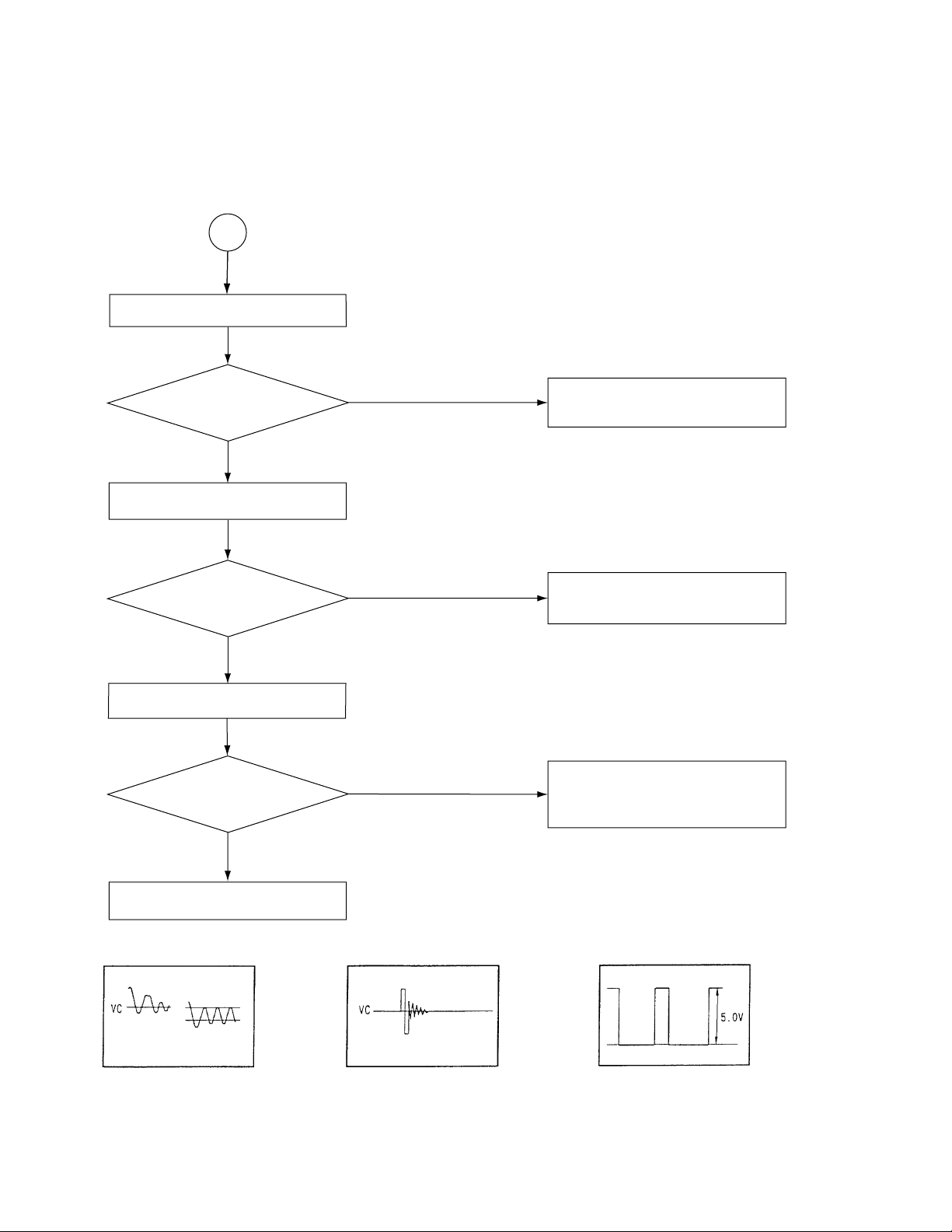
X-MDX707, XR-C2MD
4. When you cannot smoothly select music.
4
Please push 4 KEY or ¢ KEY.
Is the wave forms
of Figure 13 shown with
1 pin of IC803?.
NO
Please push 4 KEY or ¢ KEY.
NO
Is the wave forms
of Figure 14 shown with
13 pins of IC803?.
NO
Please push 4 KEY or ¢ KEY.
Is the wave forms
of Figure 15 shown with
27 pins of IC804?.
YES
YES
YES
Please readjust the E-F balance (VR802).
(Refer to the CD adjustment)
Please check the drive unit.
Please check the circumference circuit
with the solder of 29, 30, 31, 38, 39
and 40 pins of IC804.
76
NO
IC804 is broken.
Fig. 13 Fig. 14 Fig. 15
Page 77

5. When the audio signal (digital) is not sent to the output jack.
5
X-MDX707, XR-C2MD
Does a digital signal
of "H" and "L" come from
61 pins (DOUT) of IC804?.
NO
Please check
the control unit and the MD unit.
YES
Please check the circuit in the surrounding
with the solder of IC804.
IC804 is broken.
77
Page 78

X-MDX707, XR-C2MD
7.1.2 DISASSEMBLY/ASSSEMBLY
CAUTION
• Please note static electricity at the FRONT Unit(LD701, LD702)
repair.
(1)The main body
Side Panel R
(Remove as well as Side Panel L)
× 2
1
1
Side Panel L
× 3
1
2
× 2
After the slide is
done on a rear
side, Side Panel L
removes.
× 3
1
3
Front Unit
(Refer to page 79 "FRONT UNIT".)
10
10
12
10
6
STANDBY/ON
CD
OPEN/CLOSE
× 2
Drawer
10
Hook
11
Tray Panel Set
9
7
Top Panel Assy
(Refer to page 79 "TOP PANEL ASSY".)
4
4
5
4
OR
6
Minus driver
4
4
MD Unit
(Refer to page 79 "MD MECHA".)
× 2
13
8
Hook
14
× 2
13
78
Page 79

× 2
15
15
15
15
× 3
6
× 4
6
16
16
18
CD MECHA
Himelon
The CD mechanism
is drawn out while
pushing the hook.
7
TOP PANEL ASSY
7
FRONT UNIT
Insulation Sheet
Mecha Set
TUNER PCB
DECK Unit
Deck
Bracket
1
1
1
1
2
1
4
6
6
6
6
4
4
4
5
7
3
FRONT
Unit
Front Panel Set
FRONT Unit
Front
Chassis
Volume Knob
The other side of Volume Knob
The one of cylinder shape is put,
pushed, to hole of arrow of
FROUNT Unit,
and Volume Knob is removed.
The other side
of Front Panel
Set.
Hole
2
3
3
4
4
4
5
7
6
6
17
(Refer to page 80 "CD MECHA".)
7
MD MECHA
× 2
1
× 4
3
× 2
1
2
4
MD Mecha Chassis
Shield Plate
X-MDX707, XR-C2MD
79
Page 80

X-MDX707, XR-C2MD
Tension
Spring
(Door Arm)
× 2
5
Flame Main
7
8
MD Door Set
EXT Spring
6
MD Door Set
5
CAUTION
•
The CD mechanism should not disassemble when repairing and
exchanging Pick-up Unit.
When the exchange of Carriage 100, 200, 300, and the part
Clamper and something wrong with the loading operations is
repaired, it is necessary to disassemble the CD mechanism.
Please disassemble and repair according to the following
procedures.
If Tray Panel Set is not detached when the CD mechanism is
repaired, the CD mechanism cannot be removed from the main
body of the product.
When Drawer was not able not to open and shut by some
something wrong's (The power supply does not enter, etc.)
occurring, and remove Tray Panel Set, Slider 2 of the CD
mechanism is moved from the ditch of the chassis on the bottom
side of the product with a minus driver and Drawer is drawn out.
Afterwards, please remove Front Unit after removing Tray Panel
Set .
7
PICK-UP UNIT
CD MECHA
× 2
(2) CD MECHA
CD Mecha Chassis
2
10 10
× 2
1
× 2
1
MD MOUNT
9
Frame S
3
3 3
3
4
11
80
MD MOUNT
The back of CD mecha
Page 81

7
CAUTION FOR DISASSEMBLY/ASSSEMBLY OF
CD MECHA
1. As for the distinction method of Carriage100, 200, and 300,
Switch distinguishes the shape of the projection part on its back.
Please confirm the number seal pasted to the surface of
Carriage and the projection shape of the figure below when you
exchange it.
X-MDX707, XR-C2MD
Bevel Gear 4
Drawer
Assy Holder R
Carriage 100
Method of distinguishing the back of Carriage.
Method of distinguishing surface of Carriage.
2. Please do not disassemble Assy Holder L, R and the inside of
and Drawer, and do not disassemble Assy Gear Drive which
connects Assy Holder L with R.
(The position match of each gear is necessary)
3. Please do not lose the gear (Bevel Gear 4 and Gear Idler A) not
fixed while put in the axis.
Carriage 200 Carriage 300
Carriage 1001
Carriage 2002
Carriage 3003
Assy Holder L
Gear Idler A
4. Carriage 300 is put in the Chassis side, and please put in the
Drawer side without fail in order of Carriage 100 and 200.
Carriage 100, 200
Assy Gear Drive
Carriage 300
Chassis
Drawer
81
Page 82

X-MDX707, XR-C2MD
7
DRAWER
The back of Chassis
7
CHASSIS
4
The hook
is removed.
Arm
Clamper
2
Thin minus driver
etc
Carriage 300
3
Stops in the place of
which it went out by about 1cm.
8
4
5
4 to 7
The hook is removed.
Drawer
7
2
1
Assy
Slider 2
1
The loss of this gear is noted.
5
3
Arm
6
Lifter
6
Spring
7
Lifter
Spring
9
82
CONNECTOR PCB
Page 83
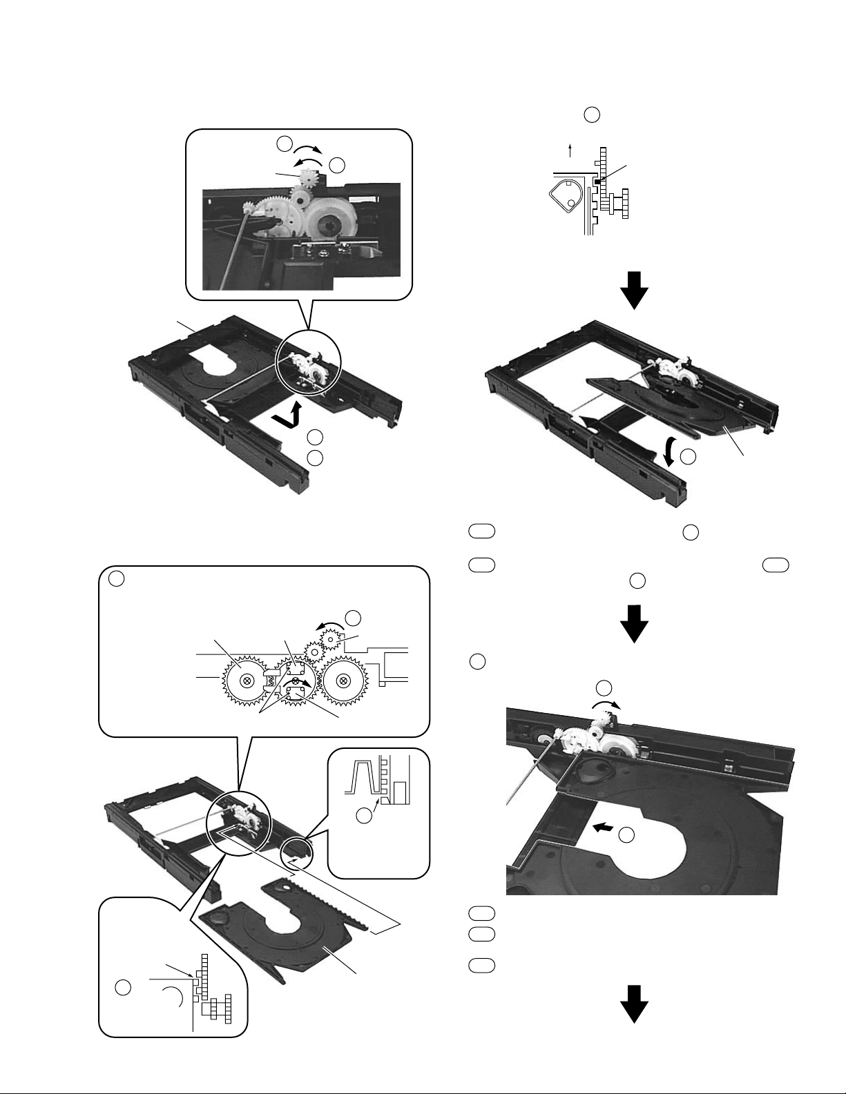
7
DISASSEMBLY OF CARRIAGE 100, 200
7
ASSSEMBLY OF CARRIAGE 100, 200
2
3
1
The loss of
Bevel Gear
is noted.
Drawer
The back of Drawer
Carriage 100
1
1
Bevel Gear
Upper Pinion
Black Cam
Lower Pinion
Mark • of Pinion of both upper and lower
must be a direction of black Cam.
(Carriage 100 is No.1 carriage. Carriage 200 is No.2 carriage.)
Bevel Gear is turned clockwise.
(direction of a rear side from a front side)
After Bevel Gear is turned counterclockwise, and five
rotations are made after lower side Pinion begins to turn,
stops in the place where its rotation stopped.
4
Carriage 200
3
The bottom of
Carriage is hit
under right Stopper
and puts.
Carriage 200
2
The first teeth of
Carriage are put
between the pin
and the pin lower
side Pinion.
Carriage
200
3
3
Hang Carriage only here of Pinion.
FRONT side
•
Notes of procedure .
4
3
5
5
6
Carriage 200
4-1
4-2 4-1
Puts Carriage 100 on Carriage 200 which applies by .
Be careful about notes by at this time.
The other side of the side applied by of Carriage is lightly
pushed.
6-1
Carriage 200 moves to a front side.
6-3
Carriage 100 drops below.
6-2
Bevel Gear is turned as it is clockwise.
(direction of a rear side from a front side)
X-MDX707, XR-C2MD
83
Page 84

X-MDX707, XR-C2MD
,
8 9
9
7
Carriage 200 is lightly
lifted by the finger.
When Carriage 100 drops below, Carriage 200 is lightly lifted
7
by the finger.
Note : Lift it horizontally when you lift Carriage.
Carriage inclines when it is not the horizontal, and
mechanism locks.
Bevel Gear is turned clockwise (direction of a rear side from
8
a front side) like the state of .
9
Carriage 200 lifts up. And, when the movement is started
Carriage 100 to the direction of a front side, separates the hand
which lifted Carriage 200.
7
7
ASSSEMBLY OF DRAWER AND CHASSIS
The following work is done before Drawer is put on Chassis.
(1) It is confirmed that Carriage 300 is clamped, and Clamper has
fallen.
(2) It is confirmed to Drawer to be built in neatly in order of Carriage
200 and 100.
(3) Arm Stopper B is moved horizontally (inside) as shown in the
figure below.
(4) Pulls Slider 2 until the lock comes off to the direction of ta front
side.
Note : Do not lift Arm Stopper B for above when you move Arm
Stopper B.
There is a possibility to bend the spring when Arm Stopper B
is lifted, and the spring bends. And, when Arm Stopper B
becomes floatage feeling, Drawer is caught.
B
Arm
Stopper
B
A
Coming off
in the spring
is noted.
A
10
Keeps turning Bevel Gear clockwise (direction of a rear side
from a front side) until Carriage 100 bumps to the wall on
a front side.
Carriage 100
The position of a right and left, black cam is matched while
11
confirming it from the table side of Drawer.
Surface of Drawer
Slider 2
Coming off of
a black gear
is noted.
Direction of front
1
This part of Drawer is put on Chassis like the arrow.
B
Drawer
1
The lock
comes off.
84
Meanwhile, Mark of right and left,
black Cam is matched.
Cam Mark Cam Mark
11
10mm is opened.
Chassis
Page 85

X-MDX707, XR-C2MD
Pulley C
Bevel Gear
Receiving
part of Gear
Drawer
Concave of Bevel Gear
Chassis hook
11
10
9
7
6
8
6
Bevel Gear is done in the slide in the middle of Pulley C and
Carriage 300.
12
13
CONNECTOR PCB
4
3
5
2
Bevel Gear
Lac teeth
Gear Idler A (black)
2
The lac teeth and Gear Idler A are matched, and it is pressed
under the diagonal lightly.
8
When peeps from the inside of Drawer when the receiving part
of Gear is fixed into the concave part of Bevel Gear, the place
where it is fixed is comprehensible.
3
Right this side of Drawer is lifted.
4
Drawer is moved back and forth, and stops Drawer with the
point which it enters left.
5
Its right side is slowly lowered up to the angle by which Bevel
Gear can do in the slide while doing Drawer back and forth by
about 5mm.
85
Page 86

X-MDX707, XR-C2MD
7.2 PARTS
7.2.1 IC
• The information shown in the list is basic information and may not correspond exactly to that shown in the schematic diagrams.
List of IC
•
0911851600 (S-8072AN-DQ-T1) , 0037502200 (CXP740096-109Q)
0911851600 (S-80727AN-DQ-T1) (CONTROL UNIT : IC902)
• High Accuracy Voltage Detector
Block Diagram
•
86
Page 87

0037502200 (CXP740096-109Q) (CONTROL UNIT : IC900)
• Main Control IC
Pin Assignment
•
X-MDX707, XR-C2MD
Block Diagram
•
87
Page 88

X-MDX707, XR-C2MD
Pin Function
•
.oNtuO/nI&kraMemaNniPO/InoitcnuF
1)O/I(5CPWR_DCLO DCLroftuptuolangiStceresetirW-daeR
2)O/I(4CPTNOCLEO tuptuolangiSlortnoCTHGIL_YEK
3)O/I(3CP3LESCSIDO tuptuolangiSlortnoCDEL3LESCSID
4)O/I(2CP2LESCSIDO tuptuolangiSlortnoCDEL2LESCSID
5)O/I(1CP1LESCSIDO tuptuolangiSlortnoCDEL1LESCSID
6)O/I(0CP-OTCENNOCON
7)I(2IS/)O/I(7BPB2TNOCLBO )EULB(tuptuolangiS2LORTNOCTHGIL-KCAB
8)I(2OS/)O/I(6BPG1TNOCLBO )NEERG(tuptuolangiS1LORTNOCTHGIL-KCAB
9)O/I()Z(2KCS/)O/I(5BPR0TNOCLBO )DER(tuptuolangiS0LORTNOCTHGIL-KCAB
01)O(2OT/)O/I(4BPGNINUTI RENUTroftupnilangiSGNINUT
11)O/I(3BPOERETSI RENUTroftupnilangiSOERETS
21)O/I(2BPKCOLC_TO RENUTroftuptuolangiSkcolclaireS
31)O/I(1BPATAD_TO/IRENUTroftuptuodnatupnilangiSatadlaireS
41)O/I(0BPDOIREPO RENUTroftuptuolangiShctallaireS
51)O/I(7JPETUMCERO tuptuolangiSlortnoCETUMCER
61)O/I(6JPSAIB_CERO tuptuolangiSlortnoCSAIBCER
71)O/I(5JPSSPTI tupnilangiSnoitceteDECAPS_CISUM
81)O/I(4JPOTOHPI tuptuolangiSrotcetedotohP
91)O/I(3JP3WSKCEDI )WSFLAHmorF(tupni3WS_KCED
02)O/I(2JP2WSKCEDI )WSR-CERmorF(tupni2WS_KCED
12)O/I(1JP1WSKCEDI )WSF-CERmorF(tupni1WS_KCED
22)O/I(0JP0WSKCEDI )WSEDOMmorF(tupni0WS_KCED
32)O/I(7DPTAEPERO tuptuolangiSNACS_CISUM
42)O/I(6DPDIONELOSO tuptuolangiSlortnoCDIONELOS
52)O/I(5DPYALP/CERO tuptuolangiSlortnoCYALP/CER
62)O/I(4DPETUM_DO tuptuolortnoCETUM_KCED
72)O/I(3DPTUCTAEBO tuptuolangiSlortnoCTUCTAEB
82)O/I(2DPYBLODO tuptuolangiSlortnoCYBLOD
92)O/I(1DPROTOMO tuptuolangiSlortnoCROTOM
03)O/I(0DPTNOCSPO tuptuolangiSlortnoCylppusrewoP
13)O(7HPEC_DNUOSO tuptuolangiSlortnoCDNUOS
23)O(6HPID_DNUPSO tuptuolangiSlortnoCDNUOS
33)O(5HPLC_DNUOSO tuptuolangiSlortnoCDNUOS
43)O(4HPETUM_SO tuptuolortnoCETUM_METSYS
53)O(3HPDC_FO tuptuolangiSlortnoCNOITCNUF_DC
63)O(2HPDM_FO tuptuolangiSlortnoCNOITCNUF_DM
73)O(1HPRENUT_FO tuptuolangiSlortnoCNOITCNUF_RENUT
83)O(0HPEPAT_FO tuptuolangiSlortnoCNOITCNUF_EPAT
93)I(1OT/)O/I(7KPXUA_FO tuptuolangiSlortnoCNOITCNUF_XUA
04)I()Z(TSRTESERI tupnilangiSTESERmetsyS
14ssVssV-ssVtcennoC
24LATXLATX- )zHM61(NIAMrofLAT'X
34)I(LATXELATXE- )zHM61(NIAMrofLAT'X
44)I()Z(SOC/)O/I(6KPTFSKLCO tuptuolangiSlortnoCTFIHS_KCOLC
54)I(0IS/)O/I(5KP1TEDSPI KCEDroftupnilangiSnoitceteDNWOD_REWOP
64)O(0OS/)O/I(4KP-IdesutoN
74)O/I()Z(0KCS/)O/I(3KP.PEEBO )%05=ytuD,zHk4=.qerF(tuptuolangiSPEEB
84)I(11NA/)O/I(7FP0TEDSPI tupnilangiSnoitceteD)CA(REWOP
94)I(01NA/)O/I(6FPLESENUT)D/A(ItupniD/AtceleSaerARENUT
05)I(9NA/)O/I(5FP1GOJVI tupnilangiSredocnEemuloV
88
Page 89

.oNtuO/nI&kraMemannIPO/InoitcnuF
15)I(8NA/)O/I(4FP0GOJVI tupnilangiSredocnEemuloV
25ssVAssVA- )retrevnocD/ArofssV(ssVtcennoC
35ferVAferVA- )retrevnocD/ArofegatlovecnerefeR(ddVtcennoC
45ddVAddVA- )retrevnocD/ArofddV(ddVtcennoC
55)I(7NA/)O/I(3FP3YEK
65)I(6NA/)O/I(2FP2YEK
75)I(5NA/)O/I(1FP1YEK
85)I(4NA/)O/I(0FP0YEK
95)I(3NA3WSYART
06)I(2NA2WSYART
16)I(1NA1WSYART
26)I(0NA0WSYART
36)I(TNIC/)O/I(7GPETUM_DCO DCroftuptuolangiSlortnoCETUM
46)I(4TNI/)O/I(6GPTEDPMETI tupnirotcetedPMET_DM
56)I(3TNI/)O/I(5GPSTC_DMI DMroftupnilangiStseuqerrefsnarT
66)I(2CE/)O/I(4GPCER_DMO tuptuolangiSlortnoCETUMCER_DM
76)I(1CE/)O/I(3GPTSR_DMO DMroftuptuolangiSTESER_DM
86)I(0CE/)O/I(2GPSTR_DMO DMroftuptuolangiStseuqerrefsnarT
96)O(DxR/)O/I(1GPDxR_DMI tupniATADlortnoCDM
07)I(DxT/)O/I(0GPDxT_DMO tuptuoATADlortnoCDM
17)O(7EP4LTC_DC
27)O(6EP3LTC_DC
37)O(5EP2LTC_DC
47)O(4EP1LTC_DC
57)O(1MWP/)O(3EPTLX_DCO DCroftuptuolangiShctallaireS
67)O(0MWP/)O(2EPKLC_DCO DCroftuptuolangiSkcolclaireS
77)I(2TNI/)I(1EPSNES_DCI DCroftupnilangiSSNES
87)I(0TNI/)I(0EPROCS_SCI DCroftupnilangiSCNYSEDOC-BUS
97)I(1IS/)O/I(7IPOSQS_DCI DCroftupnilangiSatadlaireSQBUS
08)O(1OS/)O/I(6IPATAD_DCO DCroftupnilangiSatadlaireS
18)O/I()Z(1KCS/)O/I(5IPKCQS_DCO DCroftupnilangiSkcolclaireSQBUS
28)I()Z(1SC/)O(1TNI/)O/I(4IPTSRX_DCO DCroftuptuolangiSlortnoCteseR
38)O(JDA/)O(0DT/)O/I(3IPJDAO )zHk483.61(tuptuoRELLACSERPKCOLC-BUS
48)I()Z(IMN/)O/I(2IP-IesuoN
58)O/I(CMR/)O/I(1IPETOMERI tupnilangiSlortnocetomeR
68)I(XET/)I(2KPXET-
78)I(XT/)I(1KPXT88ssVssV-ssVtcennoC
98ddVddV-ddVtcennoC
09CNCN-TCENNOCON
19)O/I(7AP7BD_DCL
29)O/I(6AP6BD_DCL
39)O/I(5AP5BD_DCL
49)O/I(4AP4BD_DCL
59)O/I(3AP3BD_DCL
69)O/I(2AP2BD_DCL
79)O/I(1AP1BD_DCL
89)O/I(0AP0BD_DCL
99)O/I(7CPE_DCLO DCLroftuptuolangiStratsetirW-daeR
001)O/I(6CPSR_DCLO DCLroftuptuolangiStceresrotsiseR
)D/A(ItupniD/AWS-YEK
)D/A(ItupniD/AWS-YART
OtuptuolangiSlortnoCrevirD
)zHk867.23(BUSroflat'X
O/IDCLrofDCLroftuptuotupnilangiSatadlellaraP
X-MDX707, XR-C2MD
89
Page 90

X-MDX707, XR-C2MD
7.2.2 DISPLAY
004044100021 (FRONT UNIT : LC700)
• LCD PANEL
Grid Assignment
•
14
1
Block Diagram
•
90
Page 91

PICT Address
•
X-MDX707, XR-C2MD
91
Page 92

X-MDX707, XR-C2MD
Interface Pin Connection
•
92
Page 93

X-MDX707, XR-C2MD
8. PANEL FACILITIES AND SPECIFICATIONS
8.1 PANEL FACILITIES
Main Unit
Display panel
Tape eject (PUSH
OPEN 0) lid
TAPE (2 3 ) button
CD (3/8) button
MD (3/8) button
TUNER FM/AM button
AUX button
•
– button
4
STANDBY/ON button
CD tray OPEN/CLOSE
CD SELECT buttons
COLOR/CLOCK button
(0) buttons
DOLBY* NR button
XR-C2MD
STOP (7) button
•
+
¢ button
MD EJECT port
MD EJECT (0) button
EDIT button
VOLUME dial
Delete/Display (DEL/
DISP) button
Jog controller (ENTER)
Headphone jack
(PHONES)
Recording mode (REC MODE) button
¶ Dolby noise reduction manufactured under license
*
from Dolby Laboratories Licensing Corporation.
TIMER button
¶ “DOLBY” and the double-D symbol are trademarks of
Dolby Laboratories Licensing Corporation.
93
Page 94
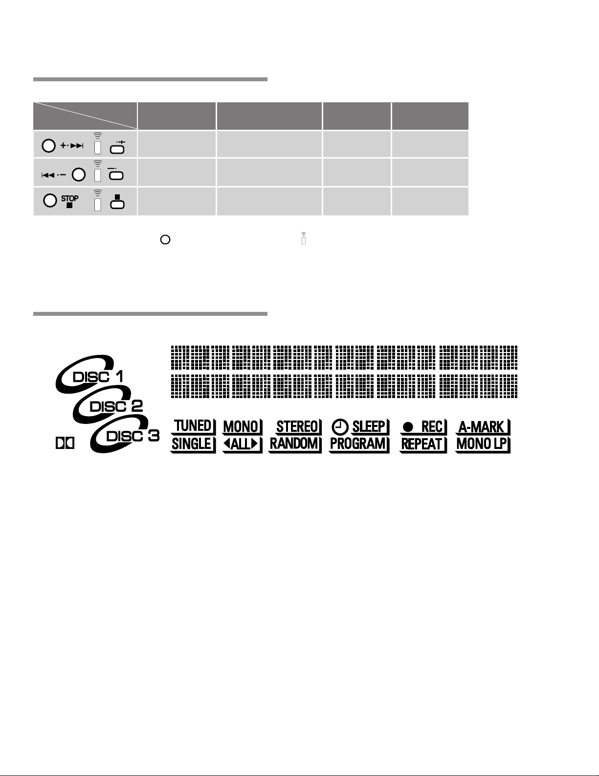
X-MDX707, XR-C2MD
Common Operation Buttons
Function of common operation buttons (the function of each button changes in accordance with the source selected)
BUTTON
Display Panel
2
SOURCE
¢
4
7
MiniDisc
Fast Forward button
Track Select button
Fast Reverse button
Track Select button
STOP button
( indicates a button on the main unit; indicates a button on the remote control unit)
Fast Forward (Rewind) button
Track Select button
Rewind (Fast Forward) button
Track Select button
STOP button
Tape
Tuner
Station Select
button
Station Select
button
Auto-Tuning
STOP button
Fast Forward button
Track Select button
Fast Reverse button
Track Select button
STOP button
CD
1
0 - = ~ ! @ # $
3
4 5 6 7 8 9
1 Alphanumeric characters display various information.
2 Indicates CD status
When a disc is loaded, the disc number lights.
During pause mode: The number of the paused CD
flashes.
3 Lights when Dolby NR is selected.
4 Lights during CD single disc play (SINGLE) mode.
5 Lights during CD all disc play (ALL) mode.
6 Lights during random play mode.
7 Lights when setting programmed contents, and during
programmed playback.
8 Flashes during 1-track repeat playback, and lights during all-
track repeat playback.
9 Lights when MiniDisc monaural (long play) recording mode is
selected.
0 Lights during AM/FM reception.
- Lights when remote control unit’s MONO button is pressed.
= Lights during reception of stereo broadcast.
~ Lights when wakeup timer is set.
Flashes when wakeup timer operates.
! Lights when sleep timer is set.
@ Lights when recording timer is set.
Flashes when recording timer operates.
# Lights during recording.
$ Lights when Auto Mark is set.
94
Page 95

Remote Control Unit
DIMMER RANDOM COLOR
DISPLAY
1 2 3 4
5 6 7 8
TAPE CD MD
4
7
9 0 - =
1 2 3 CLEAR
~
!
45 6>10
7 8 9 10/0
‡
DISP.COLOR
4
‡
TUNER
FM/AM
AUX
X-MDX707, XR-C2MD
Display Operation Buttons
1 DISPLAY button ................... Change display contents for CD and
2 DIMMER button.................... Change brightness of display.
3 RANDOM COLOR button..... Change color of display in random order.
4 COLOR button...................... Change color of display.
Function Select Buttons
5 TAPE (2 3 ) button.............. Play cassette tape or change play
6 CD (3/8) button ................... Play CD or pause playback.
7 MD (3/8) button................... Play MiniDisc or pause playback.
8 TUNER FM/AM button..........
•
9 –
4 button
0 Stop (7) button ................ Common operation buttons.
•
- ¢
+ button
= AUX button ........................... Select external auxiliary component.
MiniDisc.
direction.
Play radio broadcast or change reception
band.
)
PGM REPEAT RANDOM BEEP
@ # $ %
^ & * (
SLEEP MONO A-MARK LP/SP
123
STANDBY
/ON
CD SELECT
PLAY
MODE
SOUND
MODE
VOLUME
_ + ¡ ™
Source Operation Buttons
~ CLEAR button ...................... Erase program play contents
! Number buttons.................... Select tracks and input programming
information.
@ PGM (program) button.......... For program playback.
# REPEAT button .................... For repeat playback.
$ RANDOM button .................. For random playback.
% BEEP button......................... Set operation sound ON/OFF.
^ SLEEP button....................... Set/cancel sleep timer.
& MONO button ....................... Set FM broadcast to stereo/monaural.
* A-MARK (Auto Mark) button . Set Auto Mark function ON/OFF.
( LP/SP button ........................ Set MiniDisc recording mode.
) CD SELECT buttons............. Use to select one of 3 CDs for playback.
STANDBY/ON button
_
............. Turn power STANDBY/ON.
+ PLAY MODE button ............. Select play mode for CD, cassette tape.
¡ SOUND MODE button.......... Adjust tone.
™ VOLUME buttons ................. Adjust volume.
95
Page 96

X-MDX707, XR-C2MD
8.2 SPECIFICATIONS
7 Receiver Section
Amplifier
Continuous Power Output (RMS)
1 kHz, 10%, 6 Ω ........................................15 W + 15 W
FM Tuner
Reception frequency .............................. 87.5 - 108 MHz
Antenna .......................................75 Ω unbalanced type
AM Tuner
Reception frequency
...................................531 kHz - 1,602 kHz (9 kHz step)
.................................530 kHz - 1,700 kHz (10 kHz step)
Antenna ................. Loop antenna (furnished accessory)
7 Compact Disc Player
Type ...................................Compact Disc audio system
Usable discs ...........................................Compact Discs
Channels ........................................................ 2 (stereo)
7 Cassette Tape Deck
Track type............................... 4-track, 2-channel stereo
Recording/playback heads........................................... 1
Erase head .................................................................. 1
S/N ratio ............................................................... 50 dB
(Peak recording level, audio compensation)
With DOLBY B Type Noise Reduction .................. 1 0 d B
improvement at 5 kHz
7 MiniDisc Deck
Recording method .. Magnetic-field modulation overwrite
type
Playback method ............................. Non-contact optical
Sampling frequency ......................................... 44.1 kHz
Frequency response ............................... 20 Hz - 20 k H z
7 Power Section, Misc.
Power requirements
TAIWAN model ............................... AC 110 V, 60 Hz
Hongkong model............................. AC 220 V, 50 Hz
Power consumption
TAIWAN model ............................................... 100 W
Hongkong model............................................... 50 W
Standby power consumption.................................... 3 W
External dimensions ....160 (W) × 237 (H) × 350 (D) mm
Weight (main unit)................................................. 6.5 kg
7 Speakers
Type ..................................... Bass-reflex shelf speakers
Speaker elements (2-way type)
Woofer ............................................ 10 cm cone type
Tweeter..................................2 cm piezoelectric type
Nominal impedance ..................................................6 Ω
Frequency range .................................... 55 - 20,000 Hz
Maximum input ........................................... 20 W (EIAJ)
External dimensions ....130 (W) × 234 (H) × 226 (D) mm
Weight ..................................................................1.9 kg
7 Accessories
Operating Instructions.................................................. 1
FM T-type antenna ...................................................... 1
AM loop antenna ......................................................... 1
Remote control unit...................................................... 1
AA batteries (R6P)....................................................... 2
¶ Specifications and appearance are subject to change
without notice.
Accessories
¶ Remote control unit
96
(CU-XR043/0088041001)
‡
DISP.COLOR
7
4
RANDOM BEEP
SOUND
MODE
TUNER
FM/AM
AUX
>
VOLUME
‡
10
DIMMER RANDOM COLOR
DISPLAY
TAPE CD MD
4
1 2 3 CLEAR
456
7 8 9 10/0
PGM REPEAT
SLEEP MONO A-MARK LP/SP
123
CD SELECT
PLAY
STANDBY
MODE
/ON
¶ AM loop antenna
(illustration shows assembled unit)
(004690500013)
¶ FM T-type antenna
¶ AA/R6P batteries
(004783500013)
 Loading...