

Page 1
ORDER NO.
RRV2310
POWERED SPEAKER SYSTEM
S-DV55SW-K
S-DV55SW-Q
THIS MANUAL IS APPLICABLE TO THE FOLLOWING MODEL(S) AND TYPE(S).
Type
KUCXJI – AC120V
MVYXJI AC220-230V
This product is component of system.
S-DV55SW-K S-DV555SW-Q
Model
Power Requirement Remarks
Component System Service Manual Remarks
DVD SURROUND SYSTEM
DVD TUNER XV-DV55 RRV2309
POWERED SUBWOOFER S-DV55SW-K S-DV55SW-Q RRV2310 This service manual
SATELLITE SPEAKER
S-DV55ST-K RRV2306
S-DV55ST-Q RRV2312
CONTENTS
1. SAFETY INFORMATION..............................................................................2
2. EXPLODED VIEWS AND PARTS LIST........................................................3
3. BLOCK DIAGRAM AND SCHEMATIC DIAGRAM........................................8
4. PCB CONNECTION DIAGRAM.................................................................. 16
5. PCB PARTS LIST ....................................................................................... 23
6. ADJUSTMENT ............................................................................................25
7. GENERAL INFORMATION ........................................................................26
7.1 DISASSEMBLY ....................................................................................26
8. SPECIFICATIONS......................................................................................27
PIONEER CORPORATION 4-1, Meguro 1-chome, Meguro-ku, Tokyo 153-8654, Japan
PIONEER ELECTRONICS SERVICE, INC. P.O. Box 1760, Long Beach, CA 90801-1760, U.S.A.
PIONEER EUROPE NV Haven 1087, Keetberglaan 1, 9120 Melsele, Belgium
PIONEER ELECTRONICS ASIACENTRE PTE. LTD. 253 Alexandra Road, #04-01, Singapore 159936
c
PIONEER CORPORATION 2000
T – ZZV JUNE 2000 Printed in Japan
Page 2
S-DV55SW-K, S-DV55SW-Q
1. SAFETY INFORMATION
This service manual is intended for qualified service technicians ; it is not meant for the casual do-ityourselfer. Qualified technicians have the necessary test equipment and tools, and have been trained
to properly and safely repair complex products such as those covered by this manual.
Improperly performed repairs can adversely affect the safety and reliability of the product and may
void the warranty. If you are not qualified to perform the repair of this product properly and safely, you
should not risk trying to do so and refer the repair to a qualified service technician.
WARNING
This product contains lead in solder and certain electrical parts contain chemicals which are known to the state of California to cause
cancer, birth defects or other reproductive harm.
Health & Safety Code Section 25249.6 – Proposition 65
NOTICE
(FOR CANADIAN MODEL ONLY)
Fuse symbols (fast operating fuse) and/or (slow operating fuse) on PCB indicate that replacement parts must
be of identical designation.
REMARQUE
(POUR MODÈLE CANADIEN SEULEMENT)
Les symboles de fusible (fusible de type rapide) et/ou (fusible de type lent) sur CCI indiquent que les pièces
de remplacement doivent avoir la même désignation.
(FOR USA MODEL ONLY)
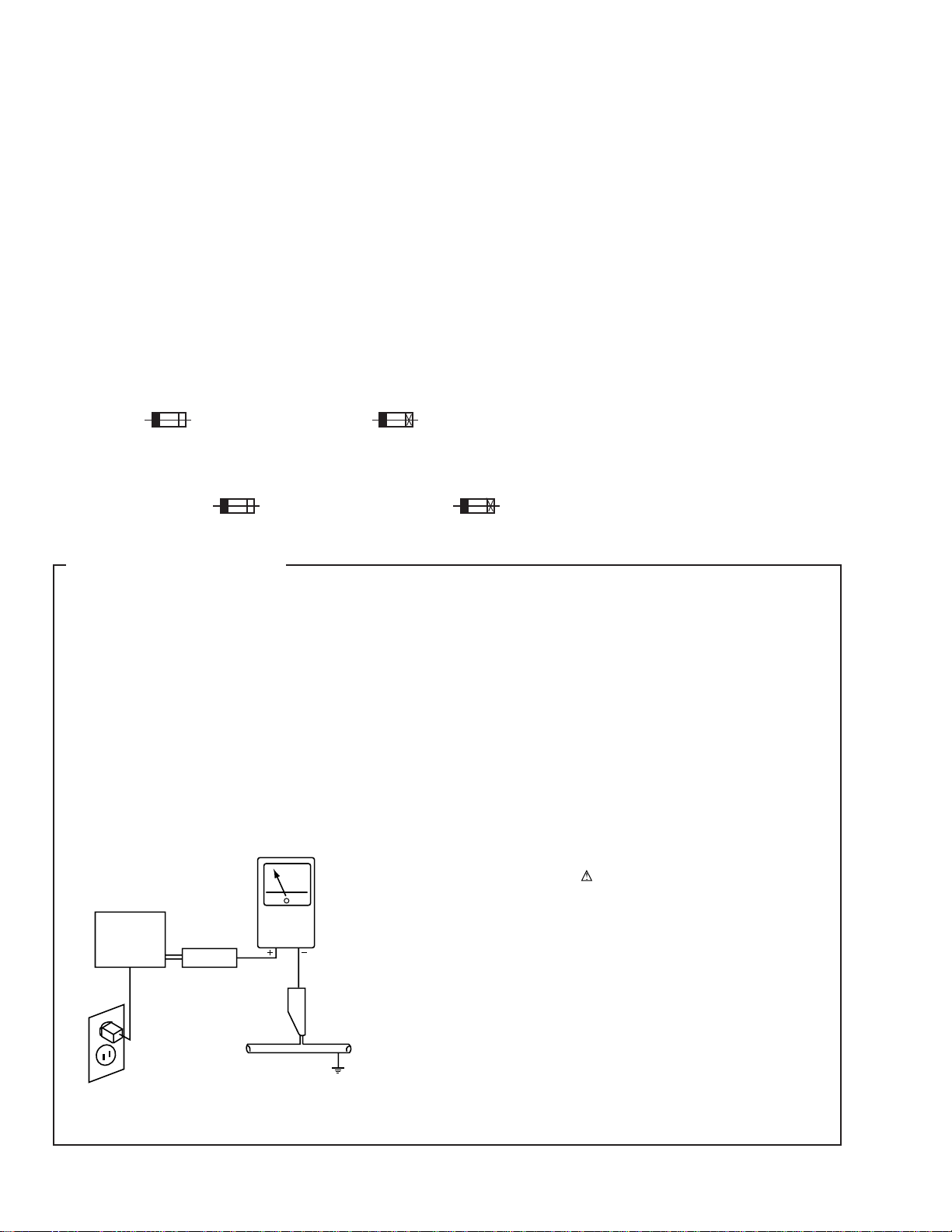
1. SAFETY PRECAUTIONS
The following check should be performed for the
continued protection of the customer and service
technician.
LEAKAGE CURRENT CHECK
Measure leakage current to a known earth ground (water
pipe, conduit, etc.) by connecting a leakage current tester
such as Simpson Model 229-2 or equivalent between the
earth ground and all exposed metal parts of the appliance
(input/output terminals, screwheads, metal overlays, control
shaft, etc.). Plug the AC line cord of the appliance directly
into a 120V AC 60Hz outlet and turn the AC power switch
on. Any current measured must not exceed 0.5mA.
Reading should
not be above
0.5mA
Earth
ground
Device
under
test
Also test with
plug reversed
(Using AC adapter
plug as required)
Leakage
current
tester
Test all
exposed metal
surfaces
ANY MEASUREMENTS NOT WITHIN THE LIMITS
OUTLINED ABOVE ARE INDICATIVE OF A POTENTIAL
SHOCK HAZARD AND MUST BE CORRECTED BEFORE
RETURNING THE APPLIANCE TO THE CUSTOMER.
2. PRODUCT SAFETY NOTICE
Many electrical and mechanical parts in the appliance
have special safety related characteristics. These are
often not evident from visual inspection nor the protection
afforded by them necessarily can be obtained by using
replacement components rated for voltage, wattage, etc.
Replacement parts which have these special safety
characteristics are identified in this Service Manual.
Electrical components having such features are identified
by marking with a
in this Service Manual.
The use of a substitute replacement component which does
not have the same safety characteristics as the PIONEER
recommended replacement one, shown in the parts list in
this Service Manual, may create shock, fire, or other hazards.
Product Safety is continuously under review and new
instructions are issued from time to time. For the latest
information, always consult the current PIONEER Service
Manual. A subscription to, or additional copies of, PIONEER
Service Manual may be obtained at a nominal charge from
PIONEER.
on the schematics and on the parts list
AC Leakage Test
2
Page 3
S-DV55SW-K, S-DV55SW-Q
2. EXPLODED VIEWS AND PARTS LIST
NOTES:• Parts marked by "NSP" are generally unavailable because they are not in our Master Spare Parts List.
The mark found on some component parts indicates the importance of the safety factor of the part.
•
Therefore, when replacing, be sure to use parts of identical designation.
Screws adjacent to mark on the product are used for disassembly.
•
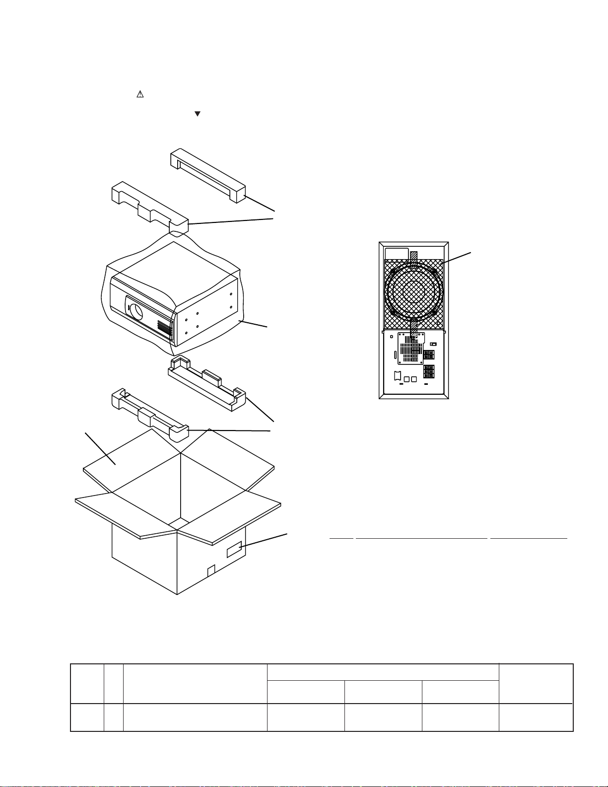
2.1 PACKING
4
5
1
2
3
(1) PACKING PARTS LIST
6
Mark No. Description Part No.
NSP 1 Poly Bag S6 SHL1250
2 Packig Case See Contrast table (2)
3 Protector (L) SHA2227
4 Protector (R) SHA2228
5 Protector SHB1090
NSP 6 Serial Barcode Label See Contrast table (2)
(2) CONTRAST TABLE
S-DV55SW-K/KUCXJI, /MVYXJI and S-DV55SW-Q/MVYXJI are constructed the same except for the following:
No.
2 Packing Case SHG2272 SHG2279 SHG2278
NSP 6 Serial Barcode Label SRM1080 Not used Not used
Symbol and Description
S-DV55SW-K S-DV55SW-K S-DV55SW-Q
/KUCXJI
Part No.
/MVYXJI
RemarksMark
/MVYXJI
3
Page 4
S-DV55SW-K, S-DV55SW-Q
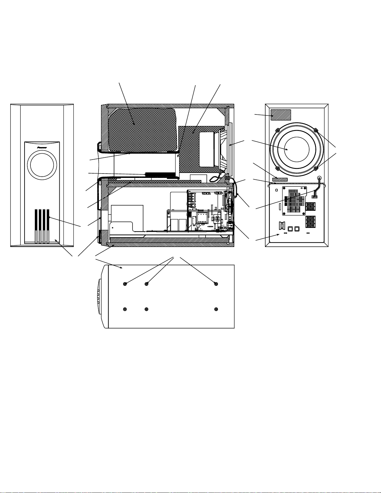
2.2 PRODUCT APPEARANCE SECTION
8
3
5
6
10
7
1
2
15
4
9
17
11
14
18
13
12
16
4
Page 5
(1) PRODUCT APPEARANCE PARTS LIST
Mark No. Description Part No.
NSP 1 Cabinet See Contrast table(2)
NSP 2 Cosmetic Duct See Contrast table(2)
NSP 3 Paper Tube SMR1320
NSP 4 Duct Ring SMR1319
5 Damper SER1279
S-DV55SW-K, S-DV55SW-Q
NSP 7 Mesh SNC1185
NSP 8 Acoustic Absorbent SMV2010
NSP 9 Acoustic Absorbent SMV1993
NSP 10 Acoustic Absorbent SMV1994
NSP 16 AMPLIFIER Assy See Contrast table(2)
NSP 17 Serial Barcode Label See Contrast table(2)
NSP 18 Serial Label See Contrast table(2)
6 Packing SEC1471
(Polyester Fiber)
(Duffel Felt)
(Duffel Felt)
11 Speaker T16EU92-52F
12 Conecting Cord SDF1086
13 Packing SEC1492
14 Screw (M4×16) (for Speaker) BYC40P160FZB
15 Screw (M4×18) BYC40P180FZB
(for Amplifier Assy fixing)
(2) CONTRAST TABLE
S-DV55SW-K/KUCXJI, /MVYXJI and S-DV55SW-Q/MVYXJI are constructed the same except for the following:
No.
NSP 1 Cabinet SMM1898 SMM1902 SMM1901
NSP 2 Cosmetic Duct SMR1323 SMR1323 SMR1314
NSP 16 AMPLIFIER ASSY * AXX7076 AXX7077 AXX7078 *Refer to 2.3 section.
NSP 17 Serial Barcode Label SRM1080 Not used Not used
NSP 18 Serial Label Not used SME3053 SME3052
Symbol and Description
S-DV55SW-K S-DV55SW-K S-DV55SW-Q
/KUCXJI
Part No.
/MVYXJI
RemarksMark
/MVYXJI
5
Page 6
S-DV55SW-K, S-DV55SW-Q
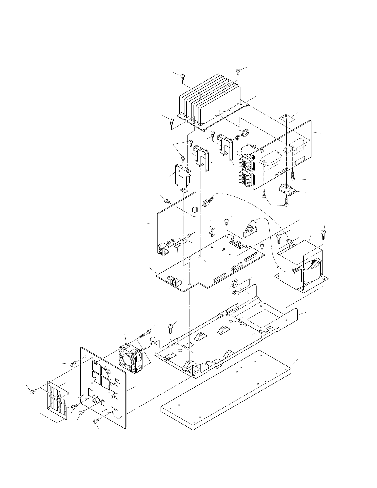
2.3 AMPLIFIER ASSY
23
23
10
11
7
A
9
24
26
23
2
24
12
26
6
23
23
23
9
23
3
23
9
8
15
21
22
20
23
27
23
19
18
13
1
16
7
5
25
A
26
4
6
Page 7
(1) AMPLIFIER ASSY PARTS LIST
Mark No. Description Part No.
1 AF Assy See Contrast table(2)
2 AMP Assy See Contrast table(2)
3 PRI Assy See Contrast table(2)
4 Wood Base AMM7005
NSP 5 Chassis ANA7109
6 Power Transformer See Contrast table(2)
NSP 7 Harness Lifter AEC7296
8 Wire Saddle AEC7297
9 Heat Sink Holder ANG7317
NSP 10 Heat Sink ANH7130
11 Mica Seat AEE7034
12 IC Holder ANG7318
13 Fuse See Contrast table(2)
14 • • • • • • •
15 Fuse Card See Contrast table(2)
16 65 Label See Contrast table(2)
17 • • • • • • •
18 Rear Panel See Contrast table(2)
19 DC Fan Motor AXM7014
20 Fan Cover AEC7280
S-DV55SW-K, S-DV55SW-Q
NSP 22 PCB Holder AEC7057
21 Nylon Rivet AEC7318
23 Screw BBZ30P080FMC
24 Screw BBZ30P140FMC
25 Screw BBZ30P300FZK
26 Screw BYC40P140FMC
27 Screw PSC30P080FNI
(2) CONTRAST TABLE
S-DV55SW-K/KUCXJI, /MVYXJI and S-DV55SW-Q/MVYXJI are constructed the same except for the following:
No.
1 AF ASSY AWU7628 AWU7631 AWU7631
2 AMP ASSY AWU7629 AWU7632 AWU7632
3 PRI ASSY AWU7627 AWU7630 AWU7630
6 Power Transformer ATS7288 ATS7289 ATS7289
13 Fuse REK1067 REK1027 REK1027
15 Fuse Card Not used AAX7493 AAX7493
16 65 Label ARW7050 Not used Not used
18 Rear Panel ANC7922 ANC7923 ANC7963
Symbol and Description
S-DV55SW-K S-DV55SW-K S-DV55SW-Q
/KUCXJI
(5A) (3.15A) (3.15A)
Part No.
/MVYXJI
RemarksMark
/MVYXJI
7
Page 8
1
1
9
8
6
2
S
23
S-DV55SW-K, S-DV55SW-Q
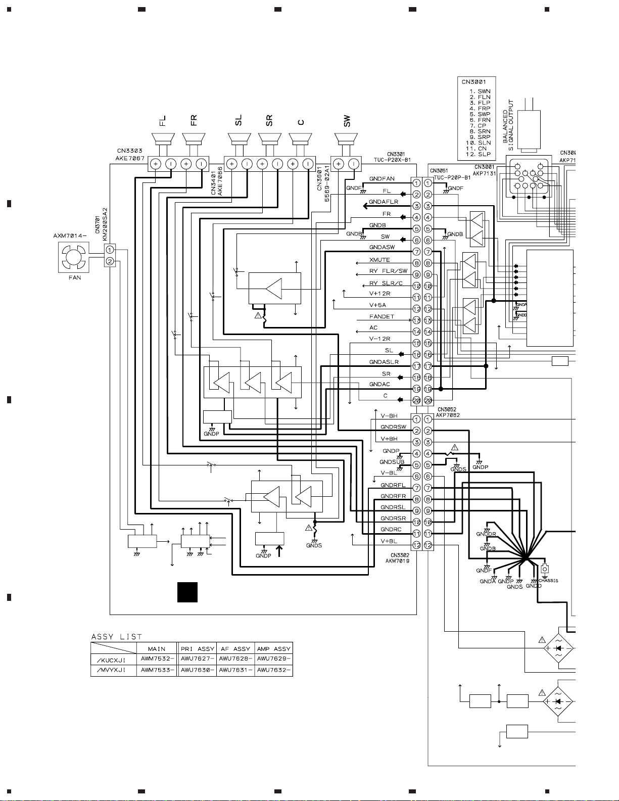
3.0 BLOCKDIAGRAM AND SCHEMATIC DIAGRAM
4
3.1 BLOCK DIAGRAM AND OVERALL CONNECTION DIAGRAM
A
GNDALR
4
1A
13
7,9,10,13
18
V+BH
2
8,15
V–BH
V+BL
819
15
91
V–BL
RY3661
RLC1
IC3601
TDA7294V
RLC2
7
14
1
IC3621
1110
STK402-240
15
RY3561
B
RY3461
RLC2
RY3461
RLC2
6
IC3401
Peripheral
Circuit
V+5A
XMUTE
RYFS
V+12R
FDET
AC
V–12R
RYRC
V+BH
IC3151
7
1
IC3161
7
1
IC3171
1
7
5
3
5
3
3
V+5D
5
V–12R
To XV-DV55
DSP ASSY
CN8901
IC3001
FL
31
FR
32
C
33
SL
34
SR
35
SW
36
37
38
39
40
41
42
V+5A
E-VOL
IC
M62446FP
Q3251
Q3252
1
1
1
1
V–BH
RY3361
RLC1
Relay Cont.
Circuit
GNDF
B
RY3361
RLC1
RLC1
RLC2
AC
RYFS
RYFR
XMUTE
GNDB
AMP ASSY (KUCXJI : AWU7629)
C
V+12R
V+12R
FDET
FAN DET.
Circuit
GNDF
V–12R
8
IC3301
10
11
STK402-040
9
V–BL
V+BL
Peripheral
Circuit
GNDALR
7
6
1
13
15
1A
IC3321
V–BL
V+BL
IC16
5A
(MVYXJI : AWU7632)
D3SBA20
D12
Q61/D61
+5V
Reg.
V+12A
V+12R
V–12A
V–12R
IC51
+12V
Reg.
NJM7812FA
IC52
–12V
Reg.
NJM7912FA
D13
AF A
S
V+5A
V+5D
D
8
1234
Page 9
5
678
S-DV55SW-K, S-DV55SW-Q
Note : When ordering service parts, be sure to refer to "EXPLODED VIEWS
and P AR TS LIST" or "PCB PARTS LIST".
V-DV55
SP ASSY
N8901
IC3001
L
31
E-VOL
32
33
IC
34
35
36
M62446FP
37
38
39
40
41
42
To XV-DV55
MOTHER ASSY
CN5592
FL
17
16
C
11
SL
9
8
SW
6
2
1
Q3251
Q3252
A
+
3
1
2
–
5
+
7
6
–
FR
IC3013
3
+
1
2
–
5
SR
+
6
7
–
IC3033
3
+
1
2
–
5
+
7
6
–
IC3053
RY41
B
D3SBA20
D11
D3SBA20
D12
D13
2V
g.
M7812FA
2V
g.
7912FA
S1WB(A)60SD
AF ASSY (KUCXJI : AWU7628)
(MVYXJI : AWU7631)
IC12
IC11
IC15
IC14
IC13
10A
10A
2.5A
2.5A
7A
A
D41
S1WB(A)60SD
C
PRI ASSY (KUCXJI : AWU7627)
(MVYXJI : AWU7630)
Not used
C
D
9
5
6
7
8
Page 10

1
S-DV55SW-K, S-DV55SW-Q
3.2 AF ASSY
AF ASSY (KUCXJI :AWU7628 ,MVYXJI :AWU7631)
A
A
B
23
(FL)
4
(SL)
(C)
SW
C
D
: Audio Signal Route
10
A
1234
Page 11

5
678
S-DV55SW-K, S-DV55SW-Q
: The power supply is shown with the marked box.
A
(FL)
(FL)
(SL)
(C)
SW
SW
CN3301
B
(SL)
B
(C)
CN13
C
CN3302
B
C
D
A
5
6
7
8
11
Page 12

1
S-DV55SW-K, S-DV55SW-Q
3.3 AMP ASSY
AMP ASSY (KUCXJI :AWU7629 ,MVYXJI :AWU7632)
B
A
(FL)
SW
23
Front Power Amp
(FL)
(FL)
4
(FL)
B
C
A
CN3051
A
CN3052
(C)
(SL)
Rear and Center
Power Amp
(SL)
(C)
SW Power Amp
(SL)
(C)
SW
D
12
B
1234
: Audio Signal Route
Page 13

(FL)
5
678
S-DV55SW-K, S-DV55SW-Q
A
(FL)
(SL)
(C)
SW
(SL)
(C)
SW
To Satellite Speaker
B
C
To Subwoofer
To FAN
D
B
5
6
7
8
13
Page 14

1
S-DV55SW-K, S-DV55SW-Q
3.4 PRI ASSY
C
PRI ASSY (KUCXJI :AWU7627 ,MVYXJI :AWU7630)
A
23
Other model use
4
B
C
A
CN12
This model use
A
CN14
D
14
C
1234
Page 15

5
• NOTE FOR FUSE REPLACEMENT
CAUTION -
FOR CONTINUED PROTECTION AGAINST RISK OF FIRE.
REPLACE WITH SAME TYPE AND RATINGS ONLY.
678
S-DV55SW-K, S-DV55SW-Q
A
B
C
D
5
6
7
8
C
15
Page 16

1
23
S-DV55SW-K, S-DV55SW-Q
3. PCB CONNECTION DIAGRAM
3.1 AF ASSY
A
NOTE FOR PCB DIAGRAMS :
1. Part numbers in PCB diagrams match those
in the schematic diagrams.
2. A comparison between the main parts of PCB
and schematic diagrams is shown below.
Symbol In PCB
Diagrams
BCE
BCE
D
B
3. The parts mounted on this PCB include all
necessary parts for several destinations.
For further information for respective destinations,
be sure to check with the schematic diagram.
4. View point of PCB diagrams.
Connector
Symbol In Schematic
Diagrams
BCEBCE
BCE
BCE
DGS
DGGSS
Capacitor
Part Name
Transistor
Transistor
with resistor
Field effect
transistor
Resistor array
3-terminal
regulator
AF ASSY
A
To Power Transformer
4
B
CN3302
C
D
P.C.Board
Chip Part
SIDE A
SIDE B
IC13 IC14 IC15
Q61
IC12 IC11
IC16
16
A
1234
Page 17

5
(
)
678
S-DV55SW-K, S-DV55SW-Q
A
302
B
CN3301
SIDE A
To
DSP ASSY
CN8901
(XV-DV55)
B
C
(ANP7365-C)
To
MOTHER ASSY
CN5592
XV-DV55
A
5
6
7
8
17
D
Page 18

1
S-DV55SW-K, S-DV55SW-Q
A
B
23
4
C
IC3012 IC3161 IC3151
IC3013IC3031
IC3032
IC3051 IC3053
IC3071
D
18
A
1234
Page 19

5
678
S-DV55SW-K, S-DV55SW-Q
A
SIDE B
B
Q3251 Q3253
5
Q3252
C
(ANP7365-C)
D
A
6
7
8
19
Page 20

1
S-DV55SW-K, S-DV55SW-Q
3.2 AMP ASSY
23
4
AMP ASSY
B
A
A
CN3052
B
SIDE A
Q3772
IC3301
IC3321
IC3621
Q3714
Q3713
IC3601
A
CN3051
Q3701
Q3702
IC3401
C
Q3651
D
(ANP7365-C)
To Satellite Speaker
To Subwoofer
20
To Satellite Speaker
B
1234
Page 21

5
678
S-DV55SW-K, S-DV55SW-Q
SIDE B
A
Q3774
Q3771
Q3773
Q3717
Q3716
Q3712
Q3711
Q3705
Q3704
Q3301
Q33302
Q3715
Q3601
Q3703 Q3706
Q3401
B
Q3402
C
Q3351 Q3352
(ANP7365-C)
5
6
7
Q3451
Q3551
Q3501
B
8
Q3452
D
21
Page 22

1
S-DV55SW-K, S-DV55SW-Q
3.3 PRI ASSY
A
C
B
23
PRI ASSY
4
SIDE A
C
(ANP7365-C)
A
CN14
D
22
C
1234
Page 23

S-DV55SW-K, S-DV55SW-Q
Mark No. Description Part No.
Mark No. Description Part No.
5. PCB PARTS LIST
NOTES:•Parts marked by "NSP" are generally unavailable because they are not in our Master Spare Parts List.
The mark found on some component parts indicates the importance of the safety factor of the part.
•
Therefore, when replacing, be sure to use parts of identical designation.
When ordering resistors, first convert resistance values into code form as shown in the following examples.
•
Ex.1 When there are 2 effective digits (any digit apart from 0), such as 560 ohm and 47k ohm (tolerance is shown by J=5%,
and K=10%).
Ex.2 When there are 3 effective digits (such as in high precision metal film resistors).
560 Ω→56 × 10
47k Ω→47 × 103→ 473 ........................................................ RD1/4PU 4 7 3 J
0.5 Ω→R50 .....................................................................................RN2H
1 Ω→1R0 .....................................................................................RS1P
5.62k Ω→ 562 × 10
CONTRAST OF PCB ASSEMBLIES
Mark
NSP AMPLIFIER ASSY AXX7076 AXX7077 AXX7078
NSP MAIN ASSY AWM7532 AWM7533 AWM7533
Symbol and Description
AF ASSY AWU7628*
AMP ASSY AWU7629 AWU7632 AWU7632
PRI ASSY AWU7627 AWU7630 AWU7630
1
→ 561 ........................................................ RD1/4PU 5 6 1 J
R 5 0
1 R 0
1
→ 5621 ...................................................... RN1/4PC 5 6 2 1 F
Part No.
S-DV55SW-K
/KUCXJI
1
S-DV55SW-K
/MVYXJI
AWU7631*
1
S-DV55SW-Q
/MVYXJI
AWU7631*
1
K
K
Remarks
*1 Constructed same.
B
AMP ASSY
AWU7629 and AWU7632 are constructed the same except for the following:
Mark
L3301,L3362,L3461,L3462,L3561 ATH-133 ATH-059
C3369,C3370,C3469,C3470,C3569,CC3669 Not used CKSQYF103Z25
C3365-C3368,C3465-C3468,C3565,C3567 Not used CKSQYF104Z25
CC3665,C3667 Not used CKSQYF104Z25
R3361,R3362,R3461,R3462 RD1/2PM100J RD1/2PM101J
R3561,R3661 RD1/2PM100J RD1/2PM101J
R3365,R3366,R3465,R3466 Not used RD1/10S100J
R3565,R3665 Not used RD1/10S100J
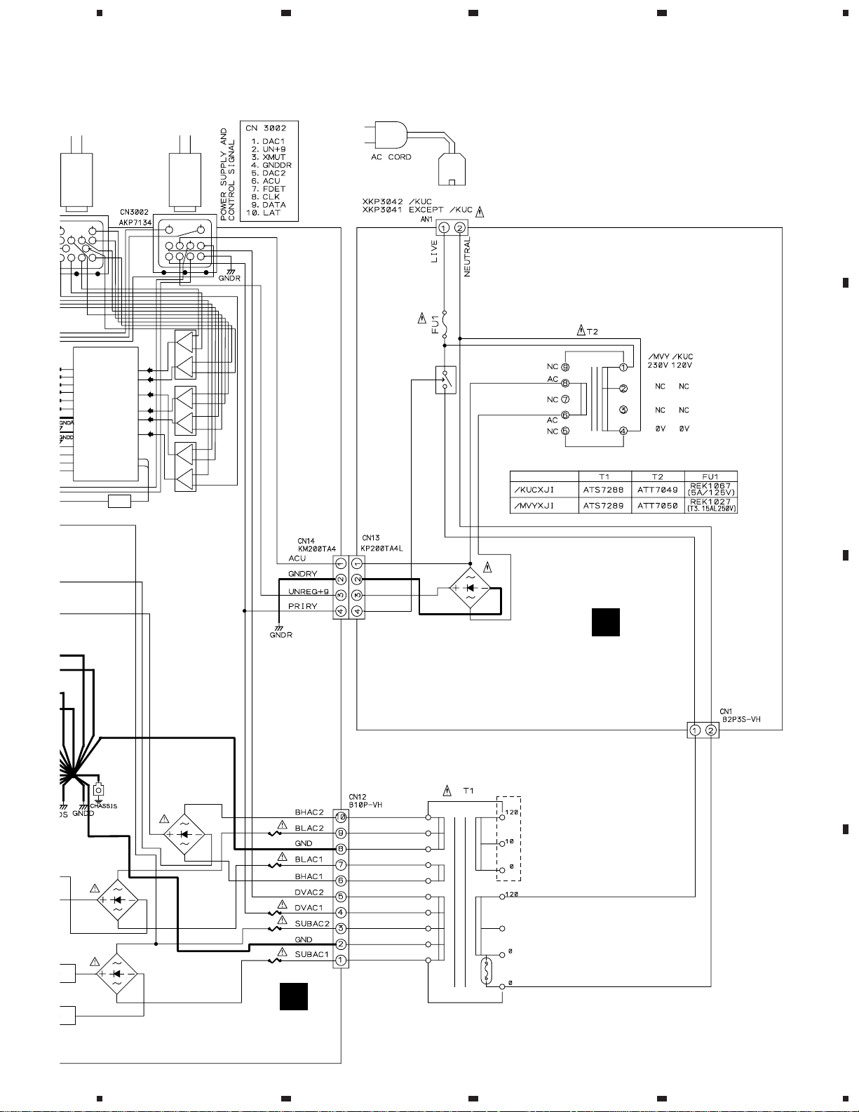
PRI ASSY
C
Symbol & Description
AWU7629
Part No.
AWU7632
AWU7627and AWU7630 are constructed the same except for the following:
Mark
Symbol & Description
T2 ATT7049 ATT7050
R1 RCN1080 Not used
AN1 XKP3042 XKP3041
KN2 VNF1084 Not used
AWU7627
Part No.
AWU7630
Remarks
Refer to page 13.
Refer to page 13.
Remarks
23
Page 24

S-DV55SW-K, S-DV55SW-Q
Mark No. Description Part No.
AF ASSY
A
SEMICONDUCTORS
IC13,IC14 (IC Protector 2.5A) AEK7014
IC16 (IC Protector 5A) AEK7019
IC11,IC12 (IC Protector 10A) AEK7022
IC51 NJM7812FA
IC52 NJM7912FA
Q61 2SD1858X
D11 D3SBA20(B)
D12 D5SBA20(B)
D13 S1WB(A)60SD
IC15 (IC Protector 7A) AEK7021
IC3013,IC3033,IC3053,IC3151 BA4558F-HT
IC3161 BA4558F-HT
IC3171 BA4558F-HT
IC3001 M62446FP
Q3251,Q3252 2SC2412K
Q3253 DTC143EK
D3251,D3252,D3254 1SS133
D3253 MTZJ2.7B
D61 MTZJ5.6B
D3203,D3204 UDZS6.8B
CAPACITORS
C71,C75 (0.01/200) ACG7021
C21,C22,C31,C32 (3300/50) ACH7098
C3006-C3008 CCSQCH101J50
C3005,C3081,C3190,C3251 CEAT100M50
C3041,C3042,C3061 CEAT1R0M50
C3021,C3022,C3157,C3158 CEAT2R2M50
C3167,C3168,C3179 CEAT2R2M50
C42 CEAT331M25
C3252,C53,C54,C61,C62 CEAT470M25
C3001,C3002,C41 CEAT471M25
C3181,C3183 CFTYA154J50
C3153,C3154,C3163,C3164,C3171 CKSQYB103K50
C3155,C3156,C3165,C3166,C3175 CKSQYB223K50
C3010,C3019,C3020,C3039,C3040 CKSQYF103Z50
C3059,C3060,C3191-C3196 CKSQYF103Z50
C51,C52 CKSQYF103Z50
C3003,C3004,C72,C76 CKSQYF473Z50
RESISTORS
R3219,R3220 RD1/2PM151J
R3254 RD1/4PM222J
R61 RD1/4PU182J
R62 RD1/4PU220J
R3909 RD1/4PU221J
R3255 RD1/4PU273J
R3015-R3026,R3035-R3046,R3055 RS1/10S1001F
R3057,R3059,R3061,R3063,R3065 RS1/10S1001F
R3075,R3077,R3079,R3081,R3083 RS1/10S1001F
R3085 RS1/10S1001F
Other Resistors RS1/10S J
Mark No. Description Part No.
CN14 4P Plug KM200TA4
CN3051 PCB connector TUC-P20P-B1
KN3001 Earth plate VNF1084
AMP ASSY (AWU7629)
B
SEMICONDUCTORS
IC3321,IC3621 (IC Protector 1A) AEK7009
IC3301 STK402-040
IC3401 STK402-240
IC3601 TDA7294V
Q3701,Q3702 2SC1740S
Q3651 2SC2240
Q3351,Q3352,Q3451,Q3452,Q3551 2SC2412K
Q3705,Q3706,Q3716,Q3717 2SC2412K
Q3301,Q3302,Q3401,Q3402,Q3501 2SD2114K
Q3601 2SD2114K
Q3772 2SD2144S
Q3713,Q3714 DTA123JS
Q3771 DTA124EK
Q3773 DTA124TK
Q3703,Q3704,Q3715 DTA143EK
Q3774 DTC124EK
Q3711,Q3712 DTC143EK
D3351-D3354,D3371,D3372 1SS133
D3452-D3454,D3551,D3553,D3653 1SS133
D3671,D3712,D3751-D3753,D3772 1SS133
D3361,D3451,D3461,D3651 1SS355
D3771 S5688G
COILS AND FILTERS
L3361,L3362,L3461,L3462,L3561 ATH-133
L3661 ATH1004
SWITCHES AND RELAYS
RY3361,RY3461,RY3561,RY3661 ASR7008
CAPACITORS
C3309,C3310,C3409,C3410,C3509 CCSQCJ3R0C50
C3307,C3308,C3321,C3322 CEAT100M50
C3407,C3408,C3421,C3422,C3507 CEAT100M50
C3601,C3751 CEAT100M50
C3712,C3713 CEAT101M10
C3771 CEAT101M25
C3323,C3324,C3423,C3424 CEAT101M35
C3621,C3622 CEAT101M50
C3331,C3607,C3625 CEAT220M50
C3301,C3302,C3401,C3402,C3501 CEAT2R2M50
C3772 CEAT2R2M50
C3711 CEAT470M25
C3609 CKSQYB102K50
C3603,C3623,C3624 CKSQYB103K50
C3305,C3306,C3405,C3406,C3505 CKSQYB221K50
C3303,C3304,C3403,C3404,C3503 CKSQYB471K50
C3361-C3364,C3461-C3464,C3561 CKSQYF104Z25
C3563 CKSQYF104Z25
C3661,C3663 CKSQYF104Z50
OTHERS
CN3052 12P Socket AKP7082
CN3001 12P Connector AKP7131
CN3002 10P Connector AKP7134
CN12 10P-VH Connector B10P-VH
24
RESISTORS
R3361,R3362,R3461,R3462,R3561 RD1/2PM100J
R3661 RD1/2PM100J
R3321,R3322,R3421,R3422 RD1/4MUF101J
R3751 RD1/4PU222J
Page 25

S-DV55SW-K, S-DV55SW-Q
Mark No. Description Part No.
R3773 RFA1/4PS330J
R3363,R3364,R3463,R3464,R3563 RS1LMF4R7J
R3663 RS1LMF4R7J
R3351,R3352,R3451,R3452,R3551 RS2LMFR22J
R3651 RS3LMFR22J
Other Resistors RS1/10S J
OTHERS
CN3601 2P Connector 5569-02A1
CN3401 6P Speaker terminal AKE7066
3303 4P Speaker terminal AKE7067
CN3302 12P Plug AKM7019
CN3301 PCB Connector TUC-P20X-B1
PRI ASSY (AWU7627)
C
SEMICONDUCTORS
D41 S1WB(A)60SD
D45 1SS133
COILS AND FILTERS
L1 ATF7018
TRANSFORMERS
T2 ATT7049
SWITCHES AND RELAYS
RY41 ASR7018
Mark No. Description Part No.
6. ADJUSTMENT
This powered subwoofer has no adjustment.
CAPACITORS
C1,C2 (0.022/AC275V) ACE7029
C44 CEAT102M25
RESISTORS
R1 RCN1080
OTHERS
CN1 2P-VH Side Connector B2P3S-VH
AN1 1P AC Inlet XKP3042
H1,H2 Huse clip AKR7001
CN13 4P Socket KP200TA4L
KN2 Earth plate VNF1084
25
Page 26

S-DV55SW-K, S-DV55SW-Q
7. GENERAL INFORMATION
7.1 DISASSEMBLY
1. Removing the Amplifier Assy
1) The Amplifier Assy is attached to the cabinet by 6 external
screws 1. To detach it, pull down the subwoofer toward the
left side.
2) Then unfasten those screws 1 .
3) Then stand up the speaker again. To detach the Amplifier Assy,
first remove the connecting code. Then pull straight the Amplifier
Assy toward back and remove it.
2. Removing the Subwoofer
1) The speaker element is attached to the back board by 4 external
screws 2.To detach it, unfasten those screws.
2) When attaching it,face its terminal downward.
Screw1
Screw1
3. Removing the Cosmetic duct
1) The cosmetic duct is attached to the baffle by press-fitting.
To detach it,pry it open by inserting a flat blade screwdriver
into lower side.
Screw2
Amplifier Assy
Screw2
Connecting Code
26
Page 27

8. SPECIFICATIONS
Amplifier Section
Subwoofer ...........................................50W (100Hz, 1% T.H.D.,8Ω)
Surround (Reference)
Front,Center,Rear ............. 30W,per channel(1KHz, 1% T.H.D.,8Ω)
Continuous power output (RMS)
Subwoofer .........................................65W (100Hz, 10% T.H.D.,8Ω)
Surround (Reference)
Front,Center,Rear ........... 40W,per channel(1KHz, 10% T.H.D.,8Ω)
Speaker Section
Powered subwoofer
Type ..............................BASS reflex floor type,antimagnetic (EIAJ)
Speaker...................................................... 16cm (6 in.) (cone type)
Nominal impedance .................................................................... 8Ω
Frequency range ..................................................... 25Hz to 300 Hz
Max. input ......................................................................65W (EIAJ)
Front, Rear, Center speakers (Reference)
Type Sealed ,antimagnetic (EIAJ)
Speaker............................................. 8.7cm (3-7/16 in.) (cone type)
Nominal impedance .................................................................... 8Ω
Frequency range .............................................. 100Hz to 20,000 Hz
Max. input ......................................................................40W (EIAJ)
S-DV55SW-K, S-DV55SW-Q
Power Supply Section
Power requirements (/KUCXJI Model) ..................... AC120V, 60Hz
Power requirements (/MVYXJI Model)......... AC220-230V, 50/60Hz
Power consumption (DVD Tuner + Powered subwoofer) ....... 178W
(/KUCXJI Model)
Power consumption (DVD Tuner + Powered subwoofer) ....... 173W
(/MVYXJI Model)
Power consumption in standby mode ......................................... 1W
Miscellaneous
Powered subwoofer unit
Dimensions ................................... 190 (W) × 425 (D) × 430 (H) mm
(7-1/2 (W) × 16-3/4 (D) × 17 (H)in.)
Weight ................................................................ 13.8 kg (30.15 lbs)
Front, Rear speakers (Reference)
Dimensions (S-DV55ST-K) .............110 (W) × 75 (D) × 154 (H) mm
(4-5/16 (W) × 2-15/16 (D) × 6 (H)in.)
Dimensions (S-DV55ST-Q).............110 (W) × 78 (D) × 154 (H) mm
Weight (S-DV55ST-K)............................................ 0.76 kg (1.7 lbs)
Weight (S-DV55ST-Q) ........................................... 0.81 kg (1.7 lbs)
Center speaker (Reference)
Dimensions (S-DV55ST-K) .............210 (W) × 75 (D) × 110 (H) mm
(8-1/2 (W) × 2-15/16 (D) × 4-5/16 (H)in.)
Dimensions (S-DV55ST-Q).............210 (W) × 78 (D) × 110 (H) mm
Weight (S-DV55ST-K)............................................ 0.83 kg (1.8 lbs)
Weight (S-DV55ST-Q) ........................................... 0.92 kg (1.8 lbs)
Note :Speciffication and the desine is subject to possible modiffication
without notice due to improvement.
27
 Loading...