

Page 1
The service manual ARP3075
was revised in October, 2000.
Please use this revised edition
instead of the 1st one.
PLASMA DISPLAY
PDP-502MX
PDP-502MXE
THIS MANUAL IS APPLICABLE TO THE FOLLOWING MODEL(S) AND TYPE(S).
Type Power Requirement
LUCBW/1 –– AC100 – 120V
YVLDK/1 –– AC100 – 240V
PDP-502MX PDP-502MXE
Model
ORDER NO.
ARP3075
Remarks
¶ This service manual should be used together with the following manual(s).
Model No. Order No. Remarks
PDP-502MX ARP3078
In PDP-502MX and PDP-502MXE, there are two different models (original model and
value analysis model) respectively. Confirm the mark and serial No. of the product Rear
side, and use each service manual. Refer to "Confirm it".
SCHEMATIC DIAGRAM, PCB DIAGRAM, PCB PARTS LIST and
IC INFORMATION
CONTENTS
Confirm it ......................................................... 2
1. SAFETY INFORMATION....................................3
2. EXPLODED VIEWS AND PARTS LIST ............. 6
3. BLOCK DIAGRAM AND SCHEMATIC DIAGRAM
.......................................................18
(For SCHEMATIC DIAGRAM, refer to ARP3078)
4. PCB DIAGRAM....................... Refer to ARP3078
5. PCB PARTS LIST................... Refer to ARP3078
6. ADJUSTMENT.................................................. 46
7. GENERAL INFORMATION .............................. 60
7.1 DIAGNOSIS................................................60
7.1.1 DIAGNOSIS METHOD......................60
7.1.2 DISASSEMBLY .................................70
7.1.3 WIRING ............................................. 72
7.2 IC ............................. Refer to ARP3078
8. PANEL FACILITIES AND SPECIFICATIONS
.......................................................76
PIONEER CORPORATION 4-1, Meguro 1-chome, Meguro-ku, Tokyo 153-8654, Japan
PIONEER ELECTRONICS SERVICE, INC. P.O. Box 1760, Long Beach, CA 90801-1760, U.S.A.
PIONEER EUROPE NV Haven 1087, Keetberglaan 1, 9120 Melsele, Belgium
PIONEER ELECTRONICS ASIACENTRE PTE. LTD. 253 Alexandra Road, #04-01, Singapore 159936
PIONEER CORPORATION 2000
T–ZZA NOV. 2000 Printed in Japan
Page 2

PDP-502MX, PDP-502MXE
Confirm it
Confirm it
PRODUCT REAR SIDE
Serial No.
(
1
∗ ∗ ∗ ∗ ∗ )
Discrimination seal
(SILVER)
SERIAL NO.
Serial No. Service Manual
1 ∗ ∗ ∗ ∗ ∗
OTHER
ARP3075 [This manual]
ARP3078
ARP3037
ARP3044
2
Page 3

PDP-502MX, PDP-502MXE
1. SAFETY INFORMATION
This service manual is intended for qualified service technicians; it is not meant for the casual
do-it-yourselfer. Qualified technicians have the necessary test equipment and tools, and have been
trained to properly and safely repair complex products such as those covered by this manual.
Improperly performed repairs can adversely affect the safety and reliability of the product and may
void the warranty. If you are not qualified to perform the repair of this product properly and safely, you
should not risk trying to do so and refer the repair to a qualified service technician.
WARNING
This product contains lead in solder and certain electrical parts contain chemicals which are known to the state of California to
cause cancer, birth defects or other reproductive harm.
Health & Safety Code Section 25249.6 – Proposition 65
NOTICE
(FOR CANADIAN MODEL ONLY)
Fuse symbols (fast operating fuse) and/or (slow operating fuse) on PCB indicate that replacement parts
must be of identical designation.
REMARQUE
(POUR MODÈLE CANADIEN SEULEMENT)
Les symboles de fusible (fusible de type rapide) et/ou (fusible de type lent) sur CCI indiquent que les
pièces de remplacement doivent avoir la même désignation.
1.1 SAFETY PRECAUTIONS
NOTICE : Comply with all cautions and safety related notes located
on or inside the cabinet and on the chassis.
The following precautions should be observed :
1. When service is required, even though the PDP UNIT an isolation
transformer should be inserted between the power line and the
set in safety before any service is performed.
2. When replacing a chassis in the set, all the protective devices
must be put back in place, such as barriers, nonmetallic knobs,
adjustment and compartment covershields, isolation resistorcapacitor, etc.
3. When service is required, observe the original lead dress. Extra
precaution should be taken to assure correct lead dress in the
high voltage circuitry area.
4. Always use the manufacture's replacement components.
Especially critical components as indicated on the circuit diagram
should not be replaced by other manufacture's.
Furthermore where a short circuit has occurred, replace those
components that indicate evidence of overheating.
5. Before returning a serviced set to the customer, the service
technician must thoroughly test the unit to be certain that it is
completely safe to operate without danger of electrical shock,
and be sure that no protective device built into the set by the
manufacture has become defective, or inadvertently defeated
during servicing. Therefore, the following checks should be
performed for the continued protection of the customer and
service technician.
6. Perform the following precautions against unwanted radiation
and rise in internal temperature.
• Always return the internal wiring to the original styling.
• Attach parts (Ground, Rear Cover, Shield Case) surely after
disassembly.
7. Perform the following precautions for the PDP panel.
• When the front case is removed, make sure nothing hits the
panel face, panel corner, and panel edge (so that the glass does
not break).
• Make sure that the panel vent does not break. (Check that the
cover is attached.)
• Handle the FPC connected to the panel carefully.
Twisting or pulling the FPC when connecting it to the connector
will cause it to peel off from the panel.
8. Pay attention to the following.
• Be sure to wire the fan. If the fan does not work, the temperature
will rise and cause the protection circuit to operate.
• When the front case is removed, infrared ray is radiated and
may disturb reception of the remote control unit.
• Pay extreme caution when the front case and rear panel are
removed because this may cause a high risk of disturbance to
TVs and radios in the surrounding.
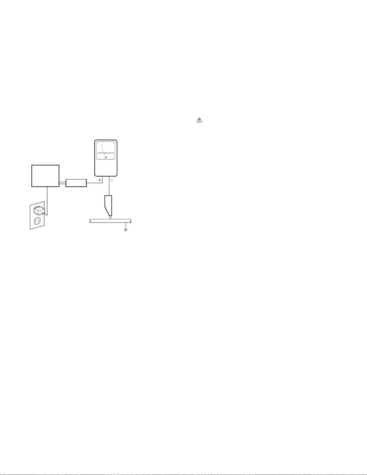
Leakage Current Cold Check
With the AC plug removed from an AC power source, place a
jumper across the two plug prongs. Turn the AC power switch on.
Using an insulation tester (DC 500V), connect one lead to the
jumpered AC plug and touch the other lead to each exposed metal
part (input/output terminals, screwheads, metal overlays, control
shafts, etc.), particularly any exposed metal part having a return
path to the chassis. Exposed metal parts having a return path to the
chassis should have a minimum resistor reading of 0.3MΩ and a
maximum resistor reading of 5MΩ. Any resistor value below or
above this range indicates an abnormality which requires corrective
action. Exposed metal parts not having a return path to the chassis
will indicate an open circuit.
3
Page 4
PDP-502MX, PDP-502MXE
Leakage Current Hot Check
Plug the AC line cord directly into an AC power source (do not use
an isolation transformer for this check).
Turn the AC power switch on.
Using a "Leakage Current Tester (Simpson Model 229 equivalent)",
measure for current from all exposed metal parts of the cabinet
(input/output terminals, screwheads, metal overlays, control shaft,
etc.), particularly any exposed metal part having a return path to the
chassis, to a known earth ground (water pipe, conduit, etc.). Any
current measured must not exceed 0.5mA.
Reading should
not be above
0.5 mA
Earth ground
Device
under
test
Also test with plug
reversed
(Using AC adapter
plug as required)
Leakage
current
tester
Test all exposed
metal surfaces
AC Leakage Test
1.2 PRODUCT SAFETY NOTICE
Many electrical and mechanical parts in PIONEER set have special
safety related characteristics. These are often not evident from
visual inspection nor the protection afforded by them necessarily
can be obtained by using replacement components rated for higher
voltage, wattage, etc. Replacement parts which have these special
safety characteristics are identified in this Service Manual.
Electrical components having such features are identified by marking
with a
Manual.
The use of a substitute replacement component which dose not have
the same safety characteristics as the PIONEER recommended
replacement one, shown in the parts list in this Service Manual, may
create shock, fire or other hazards.
Product Safety is continuously under review and new instructions
are issued from time to time. For the latest information, always
consult the current PIONEER Service Manual. A subscription to, or
additional copies of, PIONEER Service Manual may be obtained at
a nominal charge from PIONEER.
on the schematics and on the parts list in this Service
ANY MEASUREMENTS NOT WITHIN THE LIMITS
OUTLINED ABOVE ARE INDICATIVE OF A POTENTIAL
SHOCK HAZARD AND MUST BE CORRECTED BEFORE
RETURNING THE SET TO THE CUSTOMER.
4
Page 5
PDP-502MX, PDP-502MXE
1.3 CHARGED SECTION AND HIGH VOLTAGE GENERATING POINT
7 Charged Section
The places where the commercial AC power is used without
passing through the power supply transformer.
If the places are touched, there is a risk of electric shock. In addition,
the measuring equipment can be damaged if it is connected to the
GND of the charged section and the GND of the non-charged
section while connecting the set directly to the commercial AC
power supply. Therefore, be sure to connect the set via an insulated
transformer and supply the current.
7 Charged Section
(Power supply primary side)
1. AC Power Cord
2. AC Inlet with Filter
3. Power Switch (S1)
4. Fuse (In the MAIN POWER ASSY)
5. STB Transformer and Converter Transformer
(In the MAIN POWER ASSY)
6. Other primary side of the MAIN POWER ASSY
X CABLE U ASSY
CABLE ASSY
X DRIVE ASSY
X CABLE D ASSY
SIDE SW ASSY
7 High Voltage Generating Point
The places where voltage is 100V or more except for the charged
places described above. If the places are touched, there is a risk of
electric shock.
1. POWER SUPPLY MODULE (170V)
2. X DRIVE ASSY (170V)
3. Y DRIVE ASSY (–200V to 250V)
4. SCAN ASSY (250V)
For the places, refer to the EXPLODED VIEWS, the SCHEMATIC
DIAGRAM and the PCB CONNECTION DIAGRAM sections.
Part is charged section.
Part is the high voltage generating points other than the
charged section.
U-COM ASSY
CABLE ASSY
DIGIT AL VIDEO ASSY
MAIN POWER ASSY
TOP
IR RECEIVE ASSY
CABLE ASSY
CONTROL ASSY
AUDIO AMP ASSY
CABLE ASSY
VIDEO ASSY
CABLE ASSY
INPUT ASSY
CABLE ASSY
SP TERMINAL (L) ASSY
CABLE ASSY
CABLE ASSY
SCAN ASSY
Y DRIVE ASSY
5
Page 6
PDP-502MX, PDP-502MXE
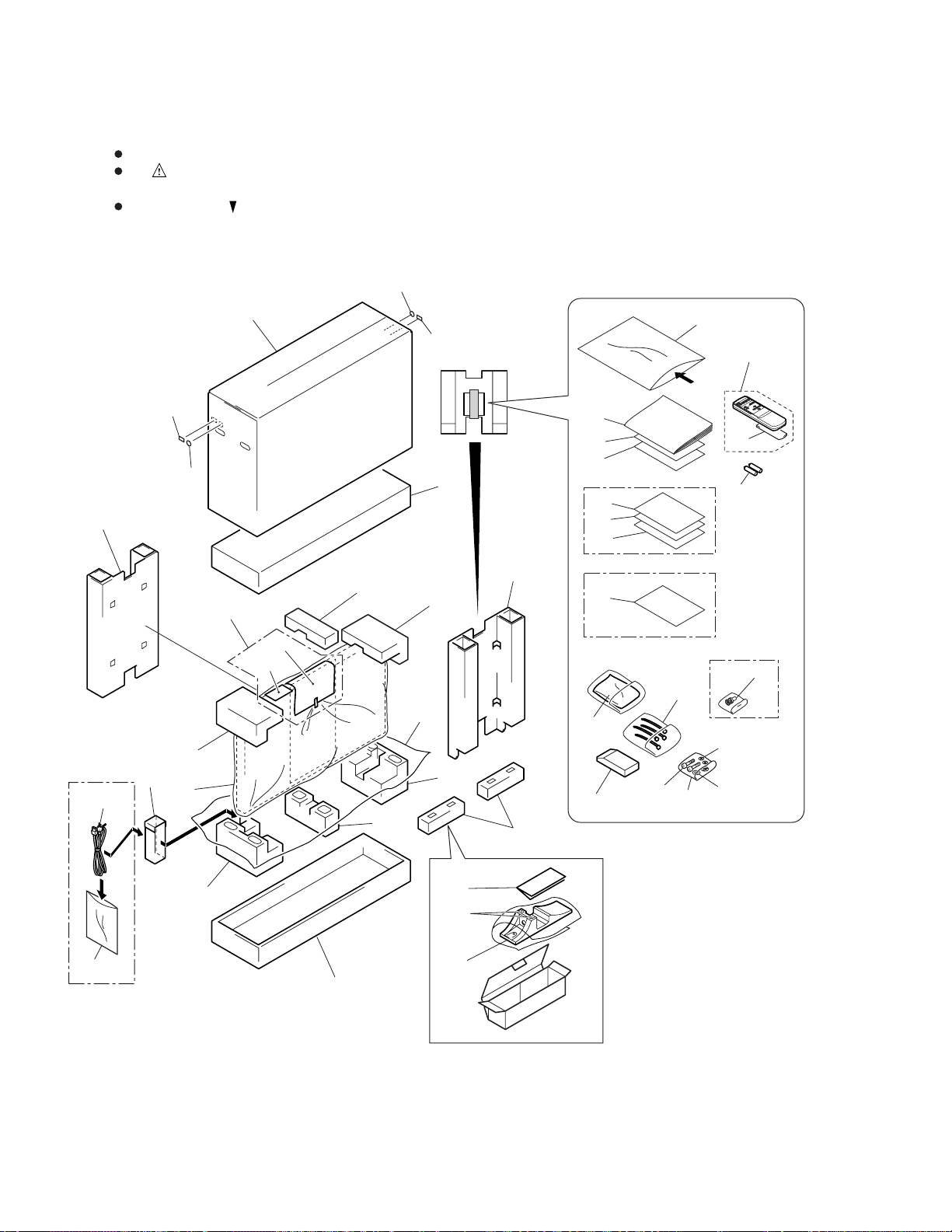
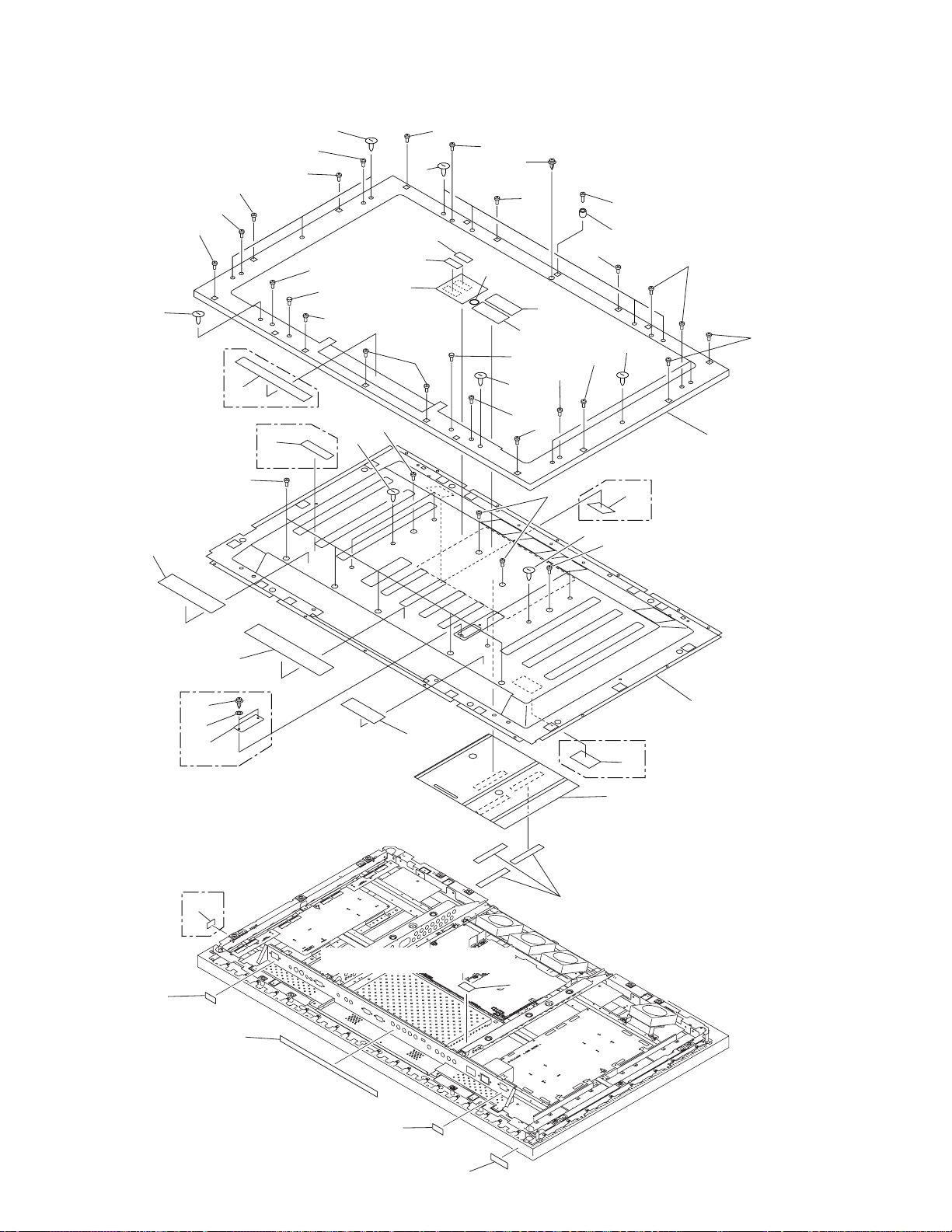
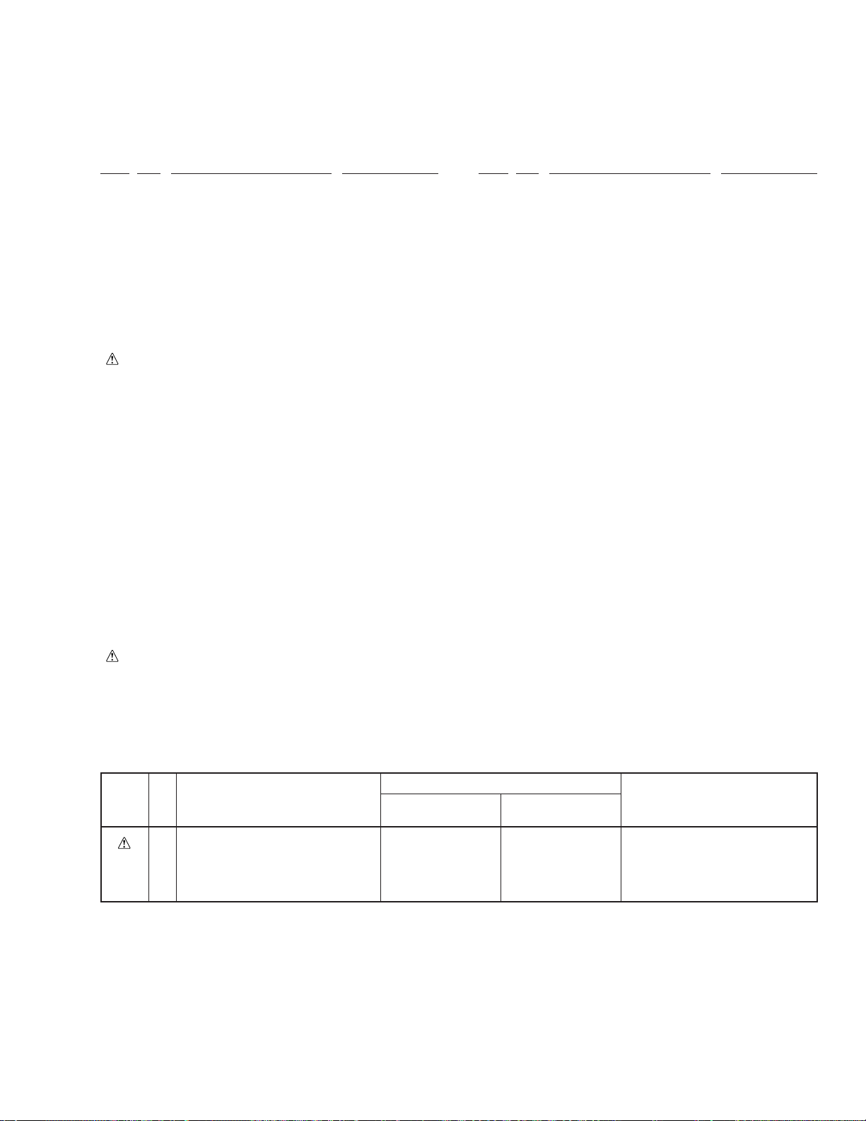
2. EXPLODED VIEWS AND PARTS LIST
NOTES : Parts marked by “ NSP ” are generally unavailable because they are not in our Master Spare Parts List.
The mark found on some component parts indicates the importance of the safety factor of the part.
Therefore, when replacing, be sure to use parts of identical designation.
Screw adjacent to mark on the product are used for disassembly.
2.1 PACKING
41
8
26
42
41
PDP-502MX Only
4
9
12
10
20, 22
21
30
42
15
18
44
11
7
5
6
3
13
1
32
16
17
19
PDP-502MX Only
40
PDP-502MXE Only
28
36
37
27
29
23
24
25
31
PDP-502MX Only
39
38
30
PDP-502MX Only
6
2
11
35
34
33
Page 7

(1) PACKING PARTS LIST
Mark No. Description Part No.
PDP-502MX, PDP-502MXE
Mark No. Description Part No.
1 Under Pad R AHA2239
2 Under Pad L AHA2240
3 Upper Pad R AHA2241
4 Upper Pad L AHA2242
5 Upper Pad C AHA2243
6 Under Pad C AHA2245
7 Front Carton AHB1210
8 Rear Carton AHB1211
9 Code Case AHC1033
10 Upper Carton
11 Under Carton AHD3037
12 Mirror Mat AHG1284
13 Polyethirene Sheet AHG1302
14 ……………………………
15 Operating Instructions
16 Plasma Caution Sheet
17 Plasma Caution Sheet
18 Caution Sheet ARM1168
19 Caution Sheet
NSP 20 Warranty Card
NSP 21 Warranty Card
NSP 22 Vinyl Pouch
23 Remote Control Unit AXD1446
(CU-V159)
24 Battery Cover AZN2098
NSP 25 AA (R6/UM-3) Batteries
See contrast table (2)
See contrast table (2)
See contrast table (2)
See contrast table (2)
See contrast table (2)
See contrast table (2)
See contrast table (2)
See contrast table (2)
See contrast table (2)
26 AC Power Cord
27 Binder Assy AEC1758
28 Cleaning Cloth AED1174
NSP 29 Vinyl Bag (for Screw, Nut) AHG-064
NSP 30 Literature Bag AHG-117
31 Pin/BNC Conversion Adaptor
32 Diaplay Stand AMR3225
NSP 33 Stand Bracket ANG2351
34 Screw CPZ30P080FZK
35 Caution Sheet ARM1175
36 Remote Control Unit Case AMR3231
37 Hex Hole Bolt (M8×40) SMZ80H400FZB
38 Washer WAX1F200K320
39 Washer WB80FZB
40 Plasma Caution Sheet
41 Seal AAX2817
NSP 42 Label VRW1629
43 Pad Set AHA2269
44 Caution Sheet ARM1194
See contrast table (2)
See contrast table (2)
See contrast table (2)
Pad set (AHA2269) is composed of the following parts.
43 Pad Set AHA2269
1 Under Pad R AHA2239
2 Under Pad L AHA2240
3 Upper Pad R AHA2241
4 Upper Pad L AHA2242
5 Upper Pad C AHA2243
6 Under Pad C AHA2245
(2) CONTRAST TABLE
PDP-502MX/LUCBW/1 and PDP-502MXE/YVLDK/1 are constructed the same except for the following:
Part No.
Mark
10 Upper Carton AHD3035 AHD3043
15 Operating Instructions ARD1039 Not used
15 Operating Instructions Not used ARE1358
16 Plasma Caution Sheet ARM1145 Not used
17 Plasma Caution Sheet ARM1147 Not used
19 Caution Sheet ARM1176 Not used
NSP 20 Warranty Card ARY1093 Not used
NSP 21 Warranty Card ARY1102 Not used
NSP 22 Vinyl Pouch AHG–195 Not used
NSP 25 AA (R6/UM-3) Batteries AEX1025 VEM1011
26 AC Power Cord ADG1178 Not used
31 Pin/BNC Conversion Adaptor AKX1052 Not used
40 Plasma Caution Sheet Not used ARM1149
Symbol and DescriptionNo.
(English/French/Japanese)
(English/French/German/Italian/
Dutch/Spanish)
PDP-502MX PDP-502MXE
LUCBW/1 YVLDK/1
Remarks
7
Page 8
PDP-502MX, PDP-502MXE
2.2 REAR CASE SECTION
4
10
PDP-502MXE
Only
PDP-502MX
Only
16
10
27 (MXE)
22
4
4
9
12
33
10
4
20
21
7
9
9
4
9
10
4
8
4
10
4
28
9
9
4
5
PDP-502MX
Only
10
9
17
4
10
27 (MX)
9
9
7
4
4
9
32
9
19 (MX)
30 (MXE)
12
31
29
PDP-502MXE
Only
PDP-502MX
Only
26
13
15
18
Refer to "2.3 EXTERIOR (1/3)".
6
PDP-502MX Only
11
3
1
24
14
25
8
Page 9

(1) REAR CASE SECTION PARTS LIST
PDP-502MX, PDP-502MXE
Mark No. Description Part No.
1 Siricon Sheet L AEH1034
2 ……………………………
3 Barrier AMR3166
4 Screw BBZ40P160FZK
5 Rear Case Frame
NSP 6 Rear Case
7 Stand Bolt ABA1277
8 Screw Collar AEC1848
9 Screw AMZ30P100FZK
10 Hole Rivet AMR2969
11 Solder Warning Label
12 Screw Rivet AEC1852
13 Terminal Label D AAX2721
14 Terminal Label F AAX2723
15 Terminal Label G
16 Terminal Label A
17 Caution Label
18 Terminal Label C
19 Terminal Label B
20 Bolt Caution Label
21 Cleaning Label
NSP 22 Name Label
23 ……………………………
See contrast table (2)
See contrast table (2)
See contrast table (2)
See contrast table (2)
See contrast table (2)
See contrast table (2)
See contrast table (2)
See contrast table (2)
See contrast table (2)
See contrast table (2)
See contrast table (2)
Mark No. Description Part No.
NSP 24 Earth Label BAX1014
25 Serial Seal AAX2609
NSP 26 Display Label
NSP 27 Label VRW1629
28 Barrier Caution Label
29 Connector Cover
30 Earth Plate
31 Washer
32 Terminal Label N
33 Seal AAX2816
34 Rear Case Service Assy
See contrast table (2)
See contrast table (2)
See contrast table (2)
See contrast table (2)
See contrast table (2)
See contrast table (2)
See contrast table (2)
Note) Rear Case Service Assy is composed of the following parts.
34 Rear Case Service Assy AWL1461 (MX)
3 Barrier AMR3166
NSP 6 Rear Case ANE1596 (MX)
11 Solder Warning Label AAX2644
20 Bolt Caution Label AAX2728
28 Barrier Caution Label AAX2759
30 Earth Plate ANK1639
AWL1457 (MXE)
ANE1587 (MXE)
(MXE only)
(MXE only)
(2) CONTRAST TABLE
PDP-502MX/LUCBW/1 and PDP-502MXE/YVLDK/1 are constructed the same except for the following:
Part No.
Mark
5 Rear Case Frame AMR3147 AMR3170
NSP 6 Rear Case ANE1596 ANE1587
11 Solder Warning Label AAX2644 Not used
15 Terminal Label G AAX2724 Not used
15 Terminal Label E Not used AAX2722
16 Terminal Label A AAX2718 Not used
16 Terminal Label L Not used AAX2734
17 Caution Label ARW1087 Not used
18 Terminal Label C AAX2720 Not used
18 Terminal Label M Not used AAX2735
19 Terminal Label B AAX2719 Not used
20 Bolt Caution Label AAX2727 AAX2728
21 Cleaning Label AAX2751 AAX2766
NSP 22 Name Label AAL2309 AAL2313
NSP 26 Display Label AAX–359 Not used
28 Barrier Caution Label AAX2759 Not used
29 Connector Cover Not used ANG2355
30 Earth Plate Not used ANK1641
31 Washer Not used ABE1077
32 Terminal Label N Not used AAX2736
34 Rear Case Service Assy AWL1461 AWL1457 Note
Symbol and DescriptionNo.
PDP-502MX PDP-502MXE
Remarks
LUCBW/1 YVLDK/1
9
Page 10
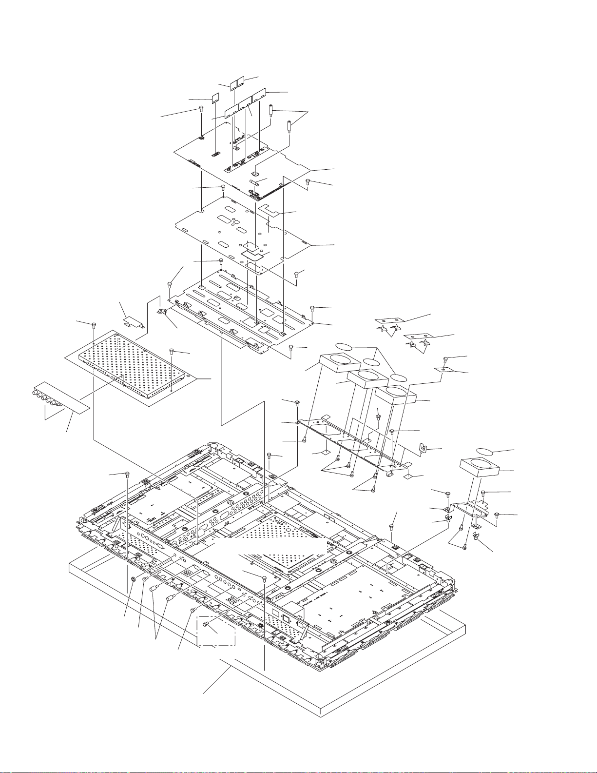
PDP-502MX, PDP-502MXE
2.3 EXTERIOR (1/3)
23
34
20
40
33
24
34
34
37
39
38
35
22
36
34
13
34
1
20
8
19
7
15
14
15
34
18
34
17
13
2
44
45
24
3
13
34
11
21
Refer to "2.4 EXTERIOR (2/3)".
43
41
42
41
Refer to "2.6 FRONT CASE SECTION".
41
PDP-502MX Only
21
12
32
21
31
32
32
21
34
30
27
10
31
9
32
14
13
20
30
27
10
Page 11
(1) EXTERIOR (1/3) SECTION PARTS LIST
PDP-502MX, PDP-502MXE
Mark No. Description Part No.
1 MAIN POWER ASSY AWZ6506
2 Fuse (10A, FU101) AEK1071
3 VIDEO ASSY
4 ……………………………
5 ……………………………
6 ……………………………
NSP 7 Chassis ANA1605
8 Insulating Sheet AMR3199
9 Fan Frame A ANG2330
10 Wire Saddle AEC1745
11 INPUT ASSY AWZ6496
NSP 12 Fan Frame C ANG2393
13 Fan Motor AXM1036
14 Fan Label AAX2785
15 Locking Card Spacer AEC1736
16 ……………………………
17 SENSOR (A) ASSY AWZ6501
18 FAN CABLE (A) ASSY AWZ6502
19 FAN CABLE (B) ASSY AWZ6497
20 Screw BMZ30P060FCU
21 Screw BBZ40P160FZK
22 Spacer Screw AEF1028
23 Wire Barrier AMR3209
24 Nylon Rivet AEC1671
25 ……………………………
See contrast table (2)
Mark No. Description Part No.
31 Fan Angle Cushion AED1193
32 Screw PPZ50P100FZK
33 PCB Hinge AEC1807
34 Screw AMZ30P060FMC
35 RCC CONTROL A ASSY AWZ6507
36 RCC CONTROL B ASSY AWZ6508
37 RCC CONTROL C ASSY AWZ6509
38 OTL CONTROL A ASSY AWZ6510
39 OTL CONTROL B ASSY AWZ6511
40 OTL CONTROL C ASSY AWZ6512
41 Screw BPZ30P080FZK
42 Hexagon Screw BBA1051
43 Nut ABN1033
44 Insulation Sheet S AMR3233
45 Insulation Sheet L AMR3234
26 ……………………………
27 PCB Mold AMR2115
28 ……………………………
29 ……………………………
30 Screw ABZ30P160FCU
(2) CONTRAST TABLE
PDP-502MX/LUCBW/1 and PDP-502MXE/YVLDK/1 are constructed the same except for the following:
Part No.
Mark
3 VIDEO ASSY AWZ6495 AWZ6516
Symbol and DescriptionNo.
PDP-502MX PDP-502MXE
Remarks
LUCBW/1 YVLDK/1
11
Page 12
PDP-502MX, PDP-502MXE
2.4 EXTERIOR (2/3)
22
18
28
20
16
23
45
24
4
38
21
23
23
26
33
23
45
15
29
13
22
4
5
26
A
12
40
23
41
13
22
22
3
2
22
1
41
14
19
37
5
19
1
31
30
32
11
23
23
12
40
22
22
21
45
A
1
39
45
23
2
Refer to "2.5 EXTERIOR (3/3)".
B
35
43
22
10
8
45
9
9
44
9
22
1
25
B
6
1
10
7
42
1
3
21
22
45
1
22
5
22
22
12
1
1
1
22
21
22
5
4
22
4
Page 13
(1) EXTERIOR (2/3) SECTION PARTS LIST
PDP-502MX, PDP-502MXE
Mark No. Description Part No.
1 Frame Shield H ANK1609
2 Frame H ANG2396
3 Frame V ANG2344
4 Frame Shield V ANK1610
5 Corner Holder ANG2347
6 Ferrite Core (L1) ATX1037
7 Sub Frame R ANG2395
8 Sub Frame L ANG2419
9 Bush C AEC1740
10 Wire Saddle AEC1745
11 AC Inlet with Filter (CN1)
12 Shield Gasket B ANK1646
13 Shield Gasket D
14 Shield Gasket C ANK1647
15 Terminal Panel
16 Shield Gasket E
17 ……………………………
NSP 18 IR Holder ANG2346
19 Edging Saddle AEC1737
20 Nylon Rivet AEC1671
21 Screw AMZ30P080FCU
22 Screw AMZ30P060FMC
23 Screw BMZ30P060FCU
24 Hexagon Screw BBA1051
25 Ferrite Core Holder AEC1818
See contrast table (2)
See contrast table (2)
See contrast table (2)
See contrast table (2)
Mark No. Description Part No.
NSP 31 Control Shield Case ANK1626
NSP 32 Control Shield Cover ANK1627
NSP 33 Control Shield Plate ANG2380
34 ……………………………
35 SP TERMINAL (L) ASSY AWZ6505
36 ……………………………
37 Spacer AEC1847
38 Screw AMZ30P100FZK
NSP 39 Drive Voltage Label ARW1097
40 Screw BPZ30P080FZK
41 Nut ABN1033
42 Screw PMB40P080FMC
43 Ferrite Core (L2) ATX1031
44 Binder AEC1851
45 Dust Guard AEB1362
26 FPC Cushion AEB1341
27 ……………………………
28 IR RECEIVE ASSY AWZ6498
29 Power Switch (S1) BSM1006
30 CONTROL ASSY AWZ6504
(2) CONTRAST TABLE
PDP-502MX/LUCBW/1 and PDP-502MXE/YVLDK/1 are constructed the same except for the following:
Part No.
Mark
11 AC Inlet with Filter (CN1) AKP1210 AKP1209
13 Shield Gasket D ANK1648 ANK1614
15 Terminal Panel ANG2341 ANG2353
16 Shield Gasket E ANK1649 ANK1634
Symbol and DescriptionNo.
PDP-502MX PDP-502MXE
Remarks
LUCBW/1 YVLDK/1
13
Page 14
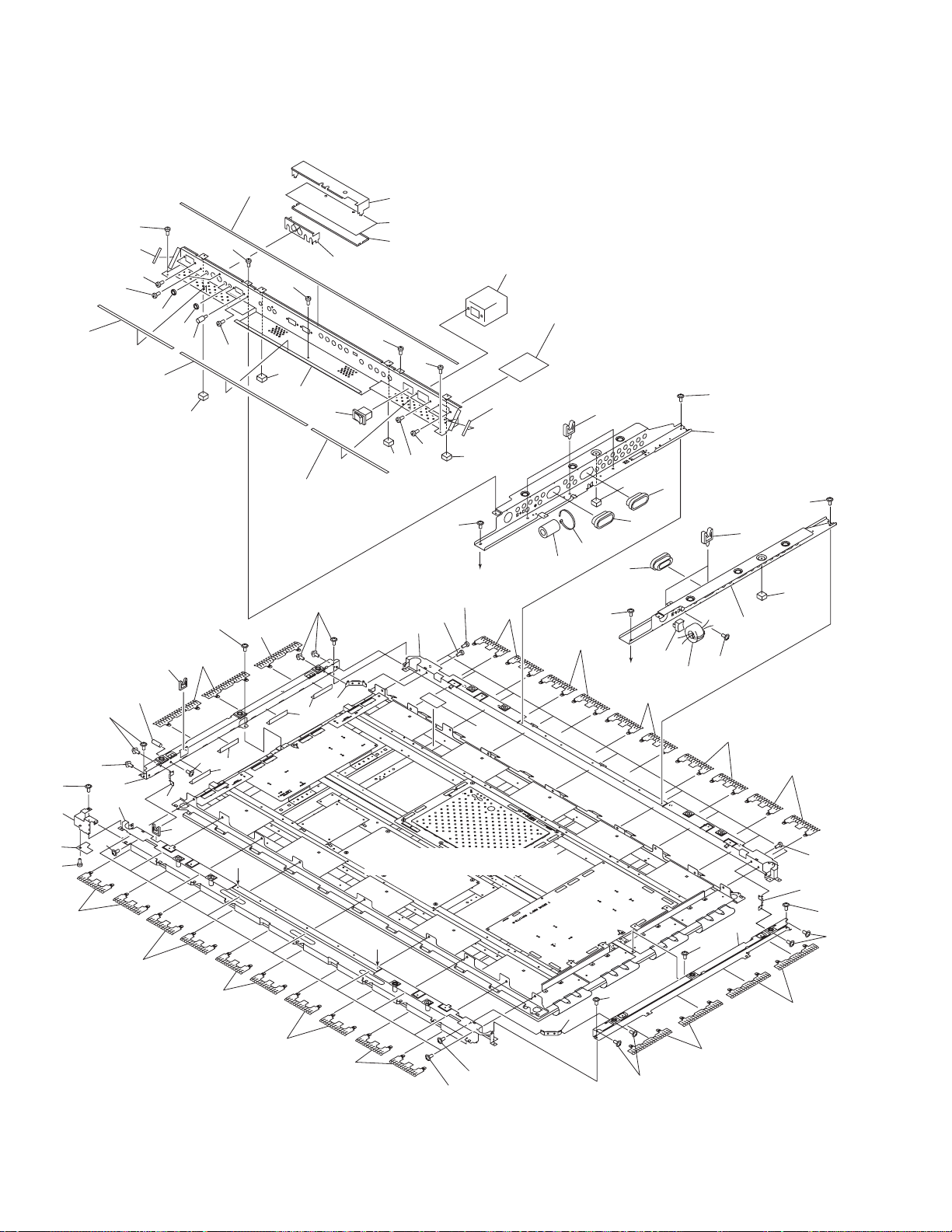
PDP-502MX, PDP-502MXE
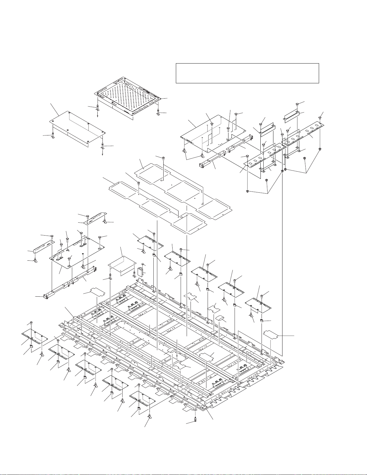
2.5 EXTERIOR (3/3)
Note*: No.47 is a special screw. Please fix to an original place.
Please never use other screws.
30
13
22
23
16
28
11
22
12
30
46
23
34
47
11
34
22
41
47
∗
39
45
9
40
9
46
23
5
11
46
11
22
40
48
36
24
46
∗
17
28
14
47
41
∗
3
39
9
47
39
15
47
28
A
28
44
44
11
2
46
23
B
1
30
∗
47
∗
32
∗
38
20
19
33
9
35
48
24
39
45
40
4
36
11
22
46
14
23
11
22
46
23
11
22
46
23
11
22
46
23
11
22
46
23
A
B
49
34
(× 40)
31
42
35
49
23
22
35
Page 15

(1) EXTERIOR (3/3) SECTION PARTS LIST
PDP-502MX, PDP-502MXE
Mark No. Description Part No.
NSP 1 Panel Shield S ANK1633
NSP 2 Panel Shield L ANK1632
NSP 3 Frame Assy ANA1633
NSP 19 Tube Cover AMR3036
NSP 20 Push Rivet AEC1748
4 SCAN (A) ASSY AWZ6518
5 SCAN (B) ASSY AWZ6519
6 ……………………………
7 ……………………………
8 ……………………………
9 PCB Spacer AMR3155
10 ……………………………
11 CABLE ASSY AWV1843
12 Y DRIVE ASSY AWV1847
13 X CABLE D ASSY AWZ6515
14 X DRIVE ASSY AWV1842
15 X CABLE U ASSY AWZ6514
16 DIGITAL VIDEO ASSY AWV1841
17 UCOM ASSY
18 ……………………………
21 ……………………………
22 Dust Guard Collar AMR3227
23 Locking Spacer AEC1794
24 Screw Grommet AEC1857
25 ……………………………
See contrast table (2)
Mark No. Description Part No.
31 Plastic Rivet AMR1066
32 AUDIO AMP ASSY AWZ6503
NSP 33 PCB Spacer AEC1446
NSP 34 Blind Sheet S AMR3202
NSP 35 Blind Sheet L AMR3203
NSP 36 Hot Plate ANG2416
37 ……………………………
38 Circuit Board Spacer AEC1795
39 Screw ABZ30P160FCU
40 Screw BBZ40P120FZK
41 Screw IBZ30P250FCU
NSP 42 Plasma Panel Assy AAV1236
43 ……………………………
44 Screw ABZ30P060FCU
45 Hot Plate Barrier AMR3223
46 Screw ABA1056
47 Screw ABA1200
48 Screw ABZ30P060FCU
49 Ferrite Core (L4, L5) ATX1041
NSP 26 ……………………………
27 ……………………………
NSP 28 Circuit Board Spacer AEC1744
29 ……………………………
30 Locking Spacer AEC1796
(2) CONTRAST TABLE
PDP-502MX/LUCBW/1 and PDP-502MXE/YVLDK/1 are constructed the same except for the following:
Part No.
Mark
17 UCOM ASSY AWZ6499 AWZ6520
Symbol and DescriptionNo.
PDP-502MX PDP-502MXE
Remarks
LUCBW/1 YVLDK/1
15
Page 16
PDP-502MX, PDP-502MXE
2.6 FRONT CASE SECTION
2
3
4
5
1
22
18
8
8
8
8
17
20
7
6
15
8
8
7
10
9
14
13
23
8
8
14
8
8
14
16
8
8
8
9
11
21
PDP-502MX
Only
14
8
14
8
8
12
8
10
8
8
7
18
9
8
8
17
16
14
11
13
8
8
9
(1) FRONT CASE SECTION PARTS LIST
Mark No. Description Part No.
1 SIDE SW ASSY AWZ6500
2 LED Lens AAK2695
3 Control Name Plate AAK2757
4 Control Shield ANK1606
5 Control Button AAC1540
6 Lens AAK2741
NSP 7 Panel Holder Assy ANG2386
8 Screw BPZ30P080FZK
9 Panel Shield H ANK1603
10 Panel Cushion H AED1189
11 Front Cushion H AED1191
12 Protect Panel Assy AMR3228
16
15
16
Mark No. Description Part No.
13 Front Cushion V AED1192
14 Corner Cushion AEB1360
15 Front Case
16 Panel Shield V ANK1604
NSP 17 Panel Holder V ANG2337
18 Panel Cushion V AED1190
19 ……………………………
NSP 20 Panel Shield VM ANK1605
21 Pioneer Seal
22 Screw BBZ30P080FMC
23 Corner Shield ANK1665
See contrast table (2)
See contrast table (2)
Page 17

PDP-502MX, PDP-502MXE
(2) CONTRAST TABLE
PDP-502MX/LUCBW/1 and PDP-502MXE/YVLDK/1 are constructed the same except for the following:
Part No.
Mark
15 Front Case AMB2649 AMB2679
21 Pioneer Seal ARW1091 Not used
Symbol and DescriptionNo.
PDP-502MX PDP-502MXE
Remarks
LUCBW/1 YVLDK/1
2.7 PDP SERVICE ASSY (AWU1030)
PDP SERVICE ASSY (AWU1030) is composed of the following parts.
Please refer to 2.4 and 2.5 for the illustrations of each part.
Mark No. Description Part No.
2.4 EXTERIOR (2/3)
1 Frame Shield H ANK1609
2 Frame H ANG2396
3 Frame V ANG2344
4 Frame Shield V ANK1610
5 Corner Holder ANG2347
21 Screw AMZ30P080FCU
22 Screw AMZ30P060FMC
26 FPC Cushion AEB1341
37 Spacer AEC1847
38 Screw AMZ30P100FZK
NSP 39 Drive Voltage Label ARW1097
2.5 EXTERIOR (3/3)
NSP 3 Frame Assy ANA1633
NSP 19 Tube Cover AMR3036
NSP 20 Push Rivet AEC1748
23 Locking Spacer AEC1794
24 Screw Grommet AEC1857
NSP 28 Circuit Board Spacer AEC1744
30 Locking Spacer AEC1796
31 Plastic Rivet AMR1066
NSP 33 PCB Spacer AEC1446
NSP 34 Blind Sheet S AMR3202
Mark No. Description Part No.
OTHERS
Wire Saddle AEC1797
Flat Clamp AEC1858
Cable Clip AEC1859
NSP FPC (XGA2-Y) ADY1047
NSP FPC (XGA2-X) ADY1053
NSP Address Mojule (IC21–IC40) MC-16340
PACKING
Button Bolt ABA1259
Corner Pad AHA2203
Corner Carton AHA2204
Upper Carton AHD2970
Under Carton AHD2971
Packing Sheet AHG1291
Holder Plate AHK1008
Washer WB80FZB
NSP 35 Blind Sheet L AMR3203
38 Circuit Board Spacer AEC1795
NSP 42 Plasma Panel Assy AAV1236
17
Page 18
1
3
2
L
Y
S
C
P
-
E
234
PDP-502MX, PDP-502MXE
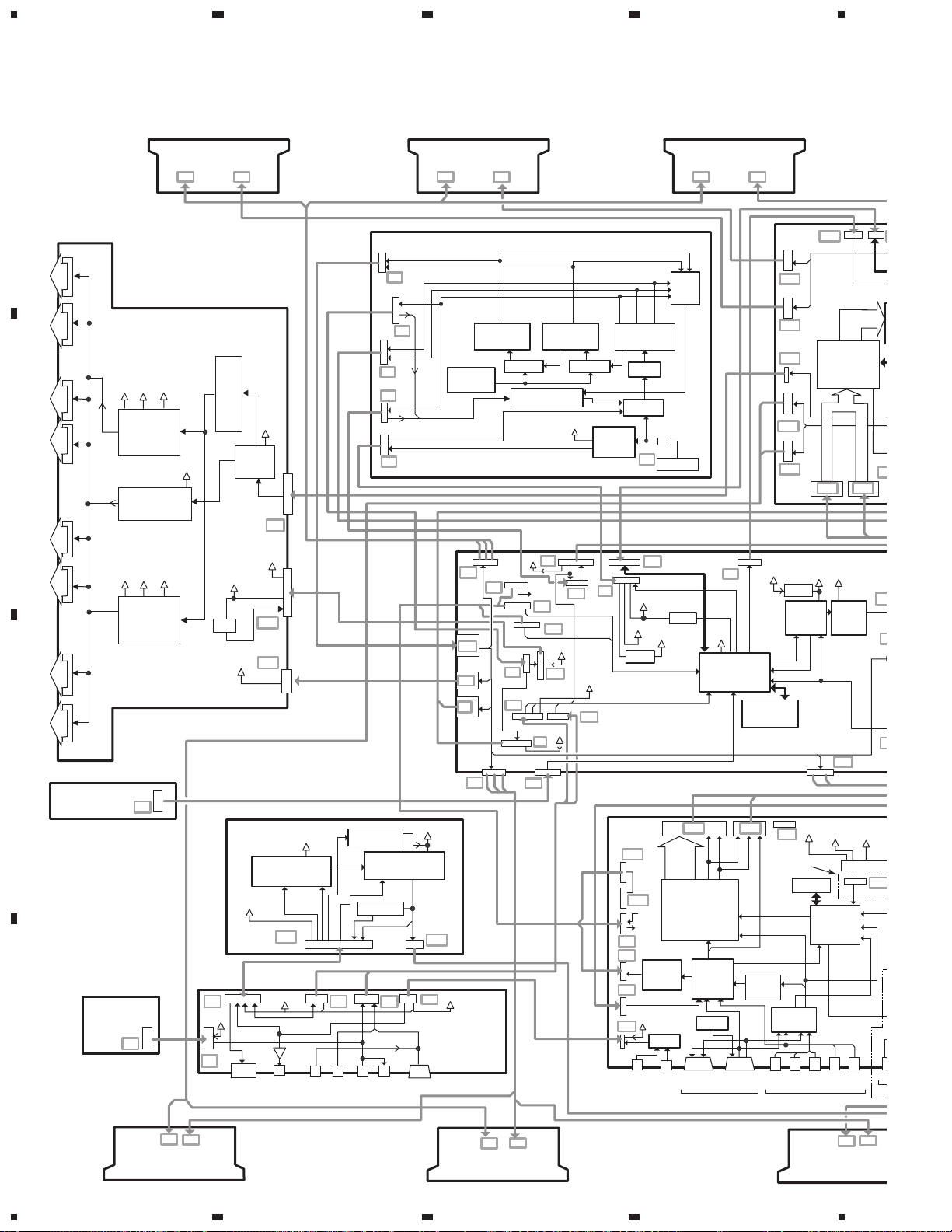
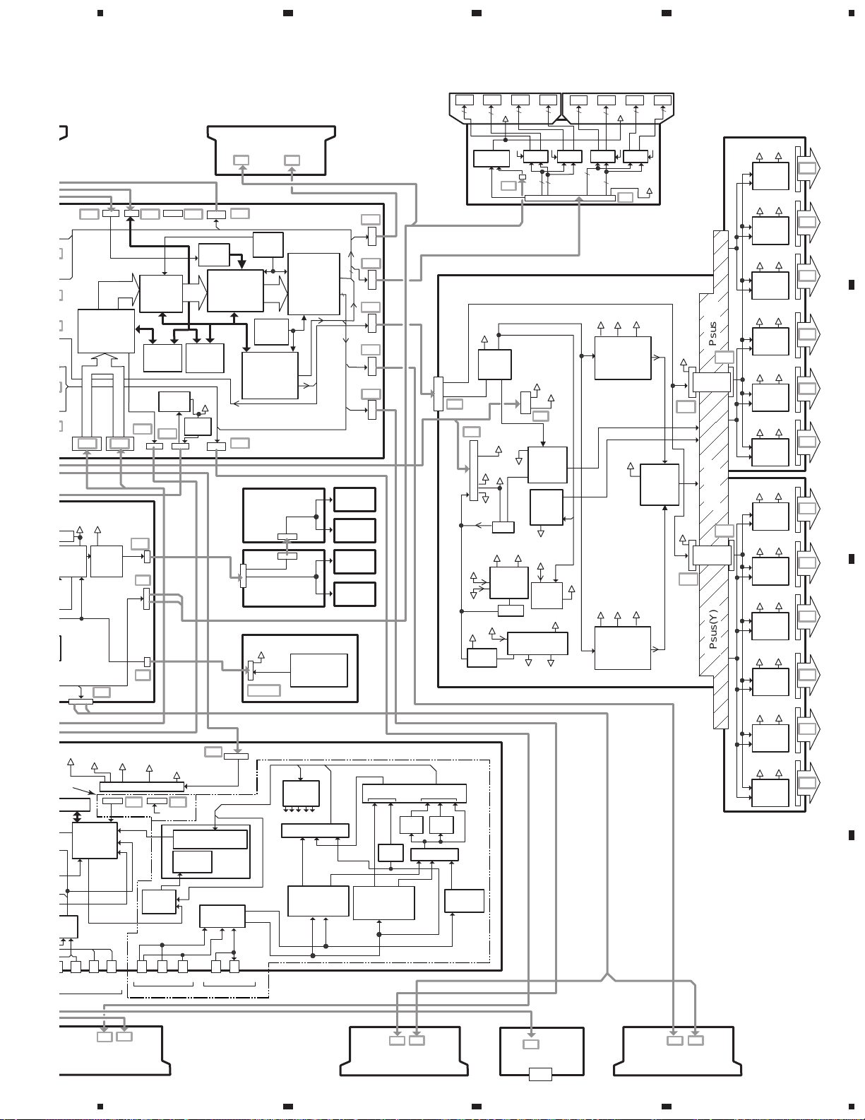
3. BLOCK DIAGRAM AND SCHEMATIC DIAGRAM
For "SCHEMATIC DIAGRAM", refer to the service manual ARP3078 for PDP-502MX.
3.1 OVERALL BLOCK DIAGRAM
A
To Panel X-Electrode
B
To Panel X-Electrode
C
SIDE SW
ASSY
D
SUS
Psus(X)
OUT
+RST
OUT
Psus(X)
SUS
OUT
Psus(X)
IR
RECEIVE
ASSY
Vsus
12V
5V
Sustain
Pulse Gen.
IC3405
Vsus
+ Reset Pulse
Gen.
5V
Vsus
12V
Sustain
Pulse Gen.
IC3402
X DRIVE ASSY
S1
U1
CABLE ASSY
K2
SUS
K1
BLK
Isolation (PC)
Logic
BLK
RST
12V
PD
OC
Vsus
AUDIO AMP ASSY
12V
STB5V
C6
S5V
R
C1
R OUT
5V
DRV
Sig.
F7
5V
F6
F5
VOL CONT
(Main/Sub)
B2
13V,S5V
REM
Audio
Out
LR
PD, VOL
12V
VOL
13V
C5
Combi
In Out
MAIN POWER ASSY
P5
P3
P6
P4
P1
CON
D-D
PWR AMP
LR
IC4502
MUTE
DC
DET
PD
R
SRInSR
L
C4
LR
Out
CABLE ASSY
K2
HI PWR
OFF SW
PWR
E35
E18
Vsus
E17
E7
Vsus
Vadr
E12
15V
B3
12V
C2
CONTROL
Tx
Rx
ASSY
K1
Vsus
Vsus
VSUS
SW PWR
PD
Vadr
E21
E1
E22
10V
PD CONT
STB5V
5V
SDA
SCK
E24
E8
E10
Vadr
VADR
SW PWR
STB12V
E3
E19
E23
5V
E16
5V
12V
DELAYDELAY
PD
STBY
PWR
12V
5V
E2
PD
13V
REM, Tx, Rx,Vol, Mute
E15
KEY, LED
8V
-8V
14V
VCC
SW PWR
+B
PFC
Relay
FU101
P7
AC IN
E5
S5V
14V
R5V
REG
DAT, CLK
SDet, FDet
U-COM ASSY
A19
A20
SDet
AMP/AD/PLL
DAT
CLK
A1
A2
Sync
U-Com
F-DET
A3
CLP,HV
12V
BLK
A5
SEL
LRLR
Audio
Audio
1/2
3/4
CABLE ASSY
K2
OC
OVC
E6
PWR
RST
S5V
SYSTEM
CONT CPU
IC3604
A33 A35
RGB
CLK
(A), (B)
HD
IC2402
HD
HD,VD
Sync
SEL
CONT
P&P
RGB
OUT
IN 4
RGB
In
CLK
K1
14V
OSD DAT
EEPROM
IC3601
HD
VD
CLP,HV
BLK
Sync
Sepa
HD
VD
Pr
D1
D19
D4
D18
D12
FAN
MAX
SD
SENS
A17
502MXE
Only
RGB
RGB
G/Y
In3/In4
SEL
R
R10V
REG
FAN
CONT
BLK
Vadr
12V
V.ROM
GYB
IN 3
D13
Process
CLP Pulse
Gen.
RGB DAT
D20 D22
Vadr
14V
FAN
DRV
E33
9V_PIC
9V_SIG
RGB
Decoder
IC1401
Y
YPbPr
HDVD
HD
CS
Pb
RGB
DAT
IP
VD
HD,VD
5APLL
5VBPLL
RGB
YCb
YPb
C
D
E
E
E
R
A30
18
K1
K2
CABLE ASSY
K2
K1
CABLE ASSY
CABLE ASS
K2
K1
1234
Page 19
CLP Pulse
Y
2
,
,
,
,
,
RGB DAT
D20 D22
14V
R10V
EG
AN
ONT
LK
adr
9V_PIC
12V
9V_SIG
MXE
ly
V.ROM
B
B
In4
L
B
Pb
RGB
Decoder
IC1401
HD
CS
IN 3
CABLE ASSY
5
67
PDP-502MX, PDP-502MXE
Notes: When ordering service parts, be sure to refer to "EXPLODED VIEWS AND PARTS LIST" or "PCB PARTS LIST".
For "PCB PARTS LIST", refer to the service manual ARP3078 for PDP-502MX.
RGB
DAT
IP
Process
Gen.
Vadr
FAN
DRV
E33
5APLL
5VBPLL
RGB
Y
YPbPr
HDVD
K1
Aspect
Conv.
FIFO
CPU
CLP
HD,VD
D17
E26
E38
E27
-5V_IO
5V_AD
REG
A30 A31
YCbCr
YPbPr
Sync
SEL
K2
D6D13 D14
OSD
Gen
RGB
DAT
IP
Panel
CPU
5V
3.3V
REG
12V
OC
UPV
D16
PD
5V_PIC
A13
5_PLD
5V_RGB
13V, 8V, -8V
SCL, SDA
Y,C
Y, Col diff Decoder
Sync
Sepa
Y
In1/In2
YCSVD
VBS
CABLE ASSY
K2
D3
Gamma-1
ABL
Dither
OSD Add
Sequence
D11
FAN CABLE B
ASSY
ASSY
R10V
SENS A
IC1201
SEL
OUT
IN 1IN 2
K1
TOP ADR DAT
(64bit * RGB * 20)
Xtal
60M
RGB
DAT
Xtal
50M
Sub-Field
MEM
Conv.
* Field
20
20
XY DRV
VADR Cont
pattern
Gen.
BOTTOM ADR DAT
(64bit * RGB * 20)
DRV
Sig
DIGITAL VIDEO ASSY
FAN A
FAN
DRV B
FAN
DRV B
FAN
DRV A
FAN CABLE A
SENSOR A ASSY
SENS
SDAT
SER
PARA
CONV.
CONT
3DY/Y/SY SEL
3DY Y
3D Y/C for
C
V/Y
V/Y
TEMP
SENS
IC4101
NTSC
FAN B
FAN C
FAN D
Y
BW_Y
3DC
C
IC IC IC IC
VADR
RGB
RGB
RGB
CLKB CLKBCLK
ADR
U/B/
D/G
VADR
Gen.
DEF DEF DEF DEF
VADR
K2
DAT3
D5
D7
Y DRIVE ASSY
D8
5V
D9
D10
DRV Sig.
H1
Logic
BLK
Vsus
10V
RN
H5
5V
- Reset
Pulse
VRN
14V
12V
Gen.
PD
-8V
OC
VFZ
D-D
CONV
BLK
OVP
D-D CONV
Vofs
12V
BLK
14V
-8V
Vsus
10V
UVP
OVP
IC5V
Vsus
Vofs
VIDEO ASSY
Y SEL C SEL
NT
PALY
SEC Y
SEC
FIL
3Line Y/C
for
PAL/60PAL
V/Y
PAL
FIL
FIL
C SEL
C
C
FILTER
C
502MX Only
K2
K1
L1
CABLE ASSY CABLE ASSY
RGB
(64bit)
Vsus
H4
OFS
Pulse
Gen.
Vcp
BLK
VRN
SP(L)
ASSY
DAT2
(64bit)
SI ,CLK
CP MSK, OFS
OFS
CP
MSK
Vcp
VH
IC IC IC IC
VADR
RGB
RGB
CLK
12V
5V
3.3V
K1
DAT1
RGB
(64bit)
DAT0
RGB
(64bit)
CABLE ASSY
5V
Vsus12V
Sustain
Pulse Gen.
IC3702
SUS
-RST
OFS
Vcp
Y-SUS
MASK
BLK
5V
Vsus12V
Sustain
SUS
Pulse Gen.
IC3707
VH
IC5V
H2
SUS OUT
VH
IC5V
H3
SUS OUT
K1
K2
8
SCAN (A) ASSY
IC5V
VH
ADD
SEL
PULSE
IC5V
VH
ADD
SEL
PULSE
IC5V
VH
ADD
SEL
PULSE
IC5V
VH
ADD
IC5V
IC5V
IC5V
IC5V
IC5V
IC5V
IC5V
IC5V
SEL
PULSE
ADD
SEL
PULSE
ADD
SEL
PULSE
ADD
SEL
PULSE
ADD
SEL
PULSE
ADD
SEL
PULSE
ADD
SEL
PULSE
ADD
SEL
PULSE
ADD
SEL
PULSE
VH
VH
VH
VH
VH
VH
VH
VH
Psus(Y)
V7
Psus(Y)
V14
Psus(Y)
SCAN (B) ASSY
A
V1
V2
V3
V4
To Panel Y-Electrode
V5
B
V6
V8
V9
V10
V11
To Panel Y-Electrode
C
V12
V13
D
L OUT
5
6
7
8
19
Page 20
1
234
PDP-502MX, PDP-502MXE
3.2 VIDEO ASSY SECTION (1/2)
A
B
C
D
R
L
AUDIO
INPUT1 (502MX)
INPUT3 (502MXE)
AUDIO
INPUT2 (502MX)
INPUT4 (502MXE)
OUTPUT
INPUT
INPUT1
C
Y
SINC
INPUT2
SINY
CN3506
Y/G
Pb/B
Pr/R
HD/CS
VD
INPUT3 (RGB1)
INPUT ASSY
(AWZ6496)
L
R
CN303
2
4
6
8
10
RGB2 INRGB2 OUT
G
R
G
R
B
B
2
4
6
8
10
To CONTROL ASSY
CN4703
IC651
1
2
4
5
11
12
14
15
FNC_1
IC102
1
2
4
5
11
12
14
15
MR_V_SW
FNC_2
5V_RGB
SCL
VD
HD
SDA
VD
HD
CN302
A5
3R
13
L
YC_VY
3
YC_C
13
IC301
Comp
IC303
Comp
IC507
(24LCS21A)
Plug & Play
ROM
IC506
15
12
10
VCLK
IC503
Comp
IC501
Comp
C2
S2_DET
2
5
7
1
3
S_DET
PDP-502MX Only
To VIDEO Assy (2/2)
A B
YC_C
YC_VY
9V_SIG
45
42YC
51
S_DET
S2_DET
+5V_RGB
9V_PIC
9V
Reg
24
12
11
23
13
5V_RGB
5V
IC305
12V
12V
Reg
4
9V_SIG
9V
Reg
PDP-502MXE Only
Y
C
FSC
HBLK_CNR
5V_PIC
Y/B–Y/R–Y DECODER SYNC SEPA.
10
SCL
SDA
SYNC
1
G1
3
B1
5
R1
HD1
VD1
7
G2
9
B2
R2
HD2
VD2
VIDEO SW
(BA7657F)
FNC_0
SAND CASTLE PULSE GEN.
HBLK/VBLK/CLP added
5V_PIC
5V
Reg
Reg
SCL
CLP_CNR
27
TV JUNGLE IC
IC1201
(TB1227BW)
4
IC1202
(TC74HC4538AF)
HOUT
4
HBLK Gen.
2MHz
LPF
21
G
19
B
15
R
22
HD
14
VD
IC306
5V_PLD
+5A_PLL
+5D_PLL
5V
5V
Reg
Reg
SDA
MAI_SW
7
5V
6
9
10
+5AD
Reg
1569
5
1
3
IC1207
SHP_SW
+3.3AD
Reg
3.3V
CN304
A31
123
SCL
SDA
37
Y
36
B–Y
35
R–Y
IC1205
(NJN1319M)
4
10
Y
Y SYNC
RGB SYNC
INT_Y
INT_Cb
INT_Cr
EXT_Y
EXT_Pb
EXT_Pr
EXT_HD
EXT_VD
K1404
–5V_IO
–5V
Reg
5
135
8V
13.5V
INT_Cr
12
Comp
7
Comp
9V_PIC
5
4
3
Multi Component Processor
11
10
RGB Matrix
(CXA2101AQ)
9
7
RGB DECODER
8
55 56 31 43
SCL
SDA
SCP
SCP Gen.
3
K2024
K2023
VD3
HD3
CN503
A30
INT_Y
INT_Cb
IC1401
K2025
HD4
9
7
11
L
VD_PLD
HD_PLD
5V_PIC
7
1
IC1204
(BA7655AF)
7976 75
P_ACL
K2013
HBLK
K2026
VD4
13
R
5
6
3
2
80
37
39
35
K2014
VBLK
20
A13
CN3401
2
567
11
1
To POWER SUPPLY ASSY
CN306
P6
1234
Page 21
5
67
8
PDP-502MX, PDP-502MXE
IN Screen K2904
NTSC 4:3 60 15.734k 40.28M Single (A) IP
PAL Wide 50 15.625k 53.63M Single (A) IP
PC
XGA (60)
B-Y_LEV
R-Y_LEV
VD_PLD
HD_PLD
IC1404
12
14
13
SEL_Vout V_STATE
G-Out
B-Out
R-Out
K2015
CLP
K2903
K2901
(VD)
(HD)
ORG 60 48.36k 32.50M Dual (A/B) Through
(CLK)
5V_PIC
Video Data
ROM
K2420
AD OUT IP Process
K2418
K2422
IC104
(24LC01B)
56
SCL
SDA
G/Y
K2004
HD_PLD
K2033
VD_PLD
K2032
K2021K2020
VD_FIL
HD_FIL
19
MMV
MMV
HD/VD
NOISE GATE
PULSE Gen.
IC2004
(TC74VHC123AFT)
12
5V_PIC
4
HBLK_MAT/VBLK_MAT/CLP_MAT
HD3/VD3/HD4/VD4
FNC_2
S_DET
R-Y_LEV
B-Y_LEV
MAT_SW
6
5432
D/A
IC2301
(CXA1875AM)
1514
K2419
FNC_0
K2421
V_STATE
HD_PLD
VD_PLD
VD_FIL
HD_FIL
HD_MASK
FNC_1
P_ACL_SW
10971
K2417
P_ACL_SW
142
110
112
102
107
106
103
VD_MASK
KU_SW
INT_RINT_R
124
INT_GINT_G
133
INT_BINT_B
139
EXT_REXT_R
126
EXT_GEXT_G
136
EXT_BEXT_B
141
K2012
K2029
K2030
Sync. Sepa for Y/G
IC2002
(M52346SP)
–HS
84
4
3
+5V_PLL
AMP/AD/PLL
(CXA3506R)
1
3
143
R
G
B
Peak ACL
12V
+VS
VD_SEP
HD_SEP
88
9896103
100
Sync. Control
Sync. Select
PLD
IC2005
(PDY069)
128
131
132
+3.3AD
+5AD
IC2402
113
111
HD_PLL
CLP_AMP
CLP_AMP
HD_PLL
HD_u, VD_u
2 22,23
5V_PIC
104
11910
106
PLL_CE
ULK_PLL
HOLD_PLL
HOLD_PLL
ULK_PLL
120
114
5V_PLD
CLK
DATA
+3.3AD
VD
137
Reset
Sync. U-COM
IC2201
(PD2060A9)
Input Freq. Det.
R (B)
G (B)
B (B)
R (A)
G (A)
B (A)
98
101
103
K2012
1_2CLK
K2012
K2012
K2012
11
XCLK
1_2CLK
HD
XCLK
HD
VD
18
19
31
16
8
8
8
8
8
K2210
4
CLK
Gate
DA_0_SV
PLL_CE
K2211
K2212
DATA
CLK
K2209
K2213
K2202
K2203
XCLK
1_2CLK
K2201
K2204
A33
CN2901
8
8
8
8
8
88
A35
CN2903
HD
VD
CN2203
A2
4
S2_DET
SDA
SCL
CLP1
CLP2
HBLK
VBLK
D20
To DIGITAL VIDEO ASSY
CN3403
1
3
D22
5
7
To DIGITAL VIDEO ASSY
CN3405
3
E24
4
5
6
To U-COM ASSY
CN3612
CN2202
A1
E23
2
3
4
5
6
To U-COM ASSY
CN2202
CN2001
A3
8
D17
9
10
11
To DIGITAL VIDEO ASSY
CN3402
A
B
C
D
SCL
SDA
21
5
6
7
8
Page 22

1
VC_YV
3D_Yin
3D_Cin
5V
REG.
LPF
(6.7MHz)
LPF
(6.7MHz)
LPF (6.7MHz)
IC803
Low Lum.
CNR
Clamp
Delay
250nS
3.58 BPF
D/A
IC703
(CXA1875AM)
SCL
SDA
54
4.43 BPF
21 345679
12
15
2
3
5
13
12
111214
2
1
3
14
4
1
15
13
4
14
131514
21435
IC1105
IC1103
IC1104
IC1004
Sin_C
3L_Vin
SCL
SDA
IC802
IC801
NTSC
NTSC
PAL
PAL
SECAM
SECAM_C
SINC
SECAM
3.3V
REG.
IC1101
(UPD64082GF-3BA)
IC1001
(CXD2064Q)
IS41C16256–35K
IC1106
LPF (6.7MHz)
4M DRAM
SECAM
Chroma Trap
5V
REG.
YC_C
1
4
768896
57
59
84
3D_Y
3D_C
18
5
4
83
60
8
CSI
AYI
3DRST
CLPO
ADIN
AYO
ACO
9
7
8
5
1
2
1
4
37
23 2517 26
FIN
MN
BPF
SW
VS
TRP1
TRP2
VS
BW
NP
MN
TRP0
TRP1
TRP0
TRP1
TRP2
DLSW
10
BPFSW
DLSW
TRP2
TRP2
VS/BW
NP
ACI
RSTB
5
IC1003
IC1002
1
4
8
5
5V_3D
5V_3D
AYO
ACO
5V_3L
5V_3L
3.3V_3D
3.3V_3D
5V_PIC
5V_SIG
TRP2
FSC
HBLK_CNR
CLP_CNRYC
SCL
SDA
8V
3D Y/C
3Line Y/C
MA (0:8)
MD (0:15)
To VIDEO Assy (1/2)
To VIDEO Assy (1/2)
3L_Y
3D_C
NTSC_C
PAL_C
A
B
234
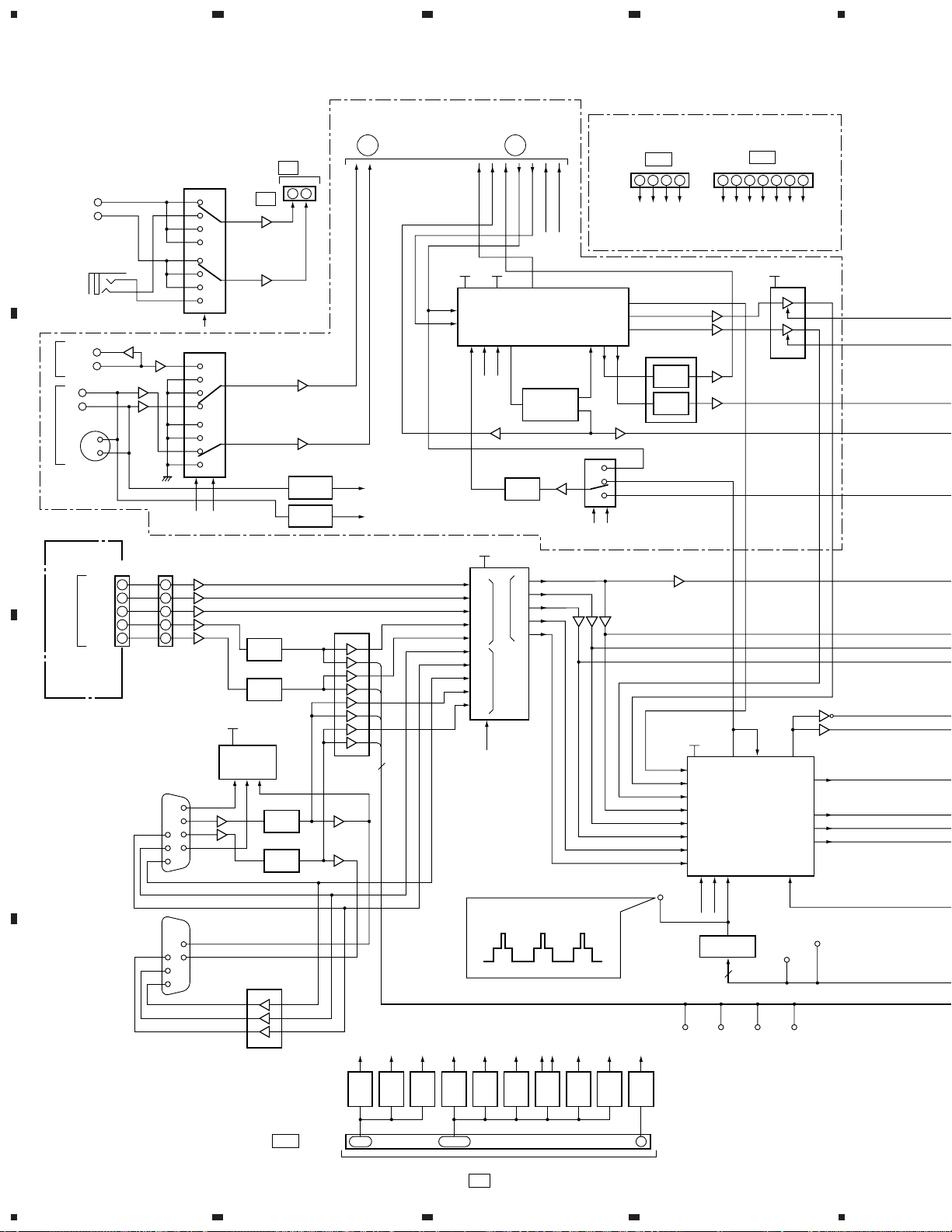
PDP-502MX, PDP-502MXE
3.3 VIDEO ASSY SECTION (2/2)
A
B
C
D
22
1234
Page 23
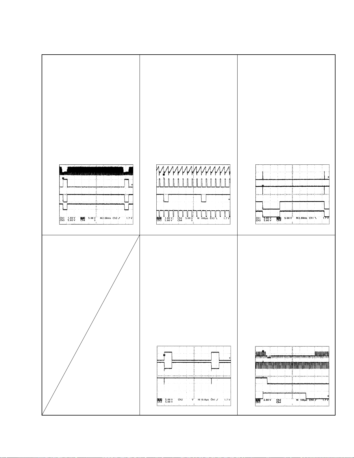
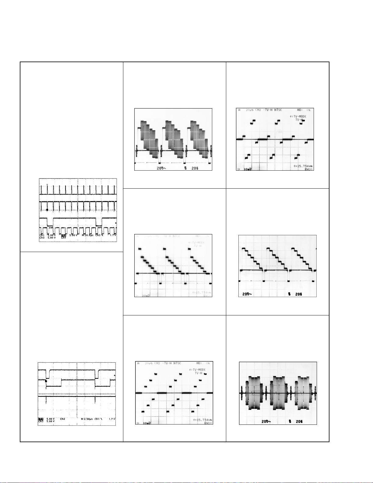
Waveforms of VIDEO ASSY
PDP-502MX, PDP-502MXE
Synchronous Signal Processing Block
(When INPUT1 NTSC RAMP signal is input)
CH1: VIDEO input
V : 1V/div H : 2msec/div
CH2: K2032 (VD_PLD), IC2005 Pin 112
V : 5V/div H : 2msec/div
CH3: K2018 (VD_u), IC2005 Pin 34
V : 5V/div H : 2msec/div
CH4: K2031 (VD_DSEL), IC2005 Pin 137
V : 3.3V/div H : 2msec/div
Synchronous Signal Processing Block
(When INPUT1 NTSC RAMP signal is input)
CH1: VIDEO input
V : 1V/div H : 100msec/div
CH2: K2033 (HD_PLD), IC2005 Pin 110
V : 5V/div H : 100msec/div
CH3: K2019 (HD_u), IC2005 Pin 32
V : 5V/div H : 100msec/div
CH4: K2029 (HD_PLL), IC2005 Pin 118
V : 3.3V/div H : 100msec/div
Synchronous Signal Processing Block 2
(INPUT4 PC siganl VESA:
1280x1024@60Hz (SXGA@60Hz)
when there is signal input [ separate H, V ]
CH1: K2026 (VD_4),
IC2005 Pin71 (VD input)
V: 5V/div H: 2msec/div
CH2: K2020 (VD_FIL), IC2005 Pin 102
V: 5V/div H: 2msec/div
CH3: K2018 (VD_u), IC2005 Pin 34
V : 5V/div H : 2msec/div
CH4: K2031 (VD_DSEL), IC2005 Pin 137
V : 3.3V/div H : 2msec/div
Synchronous Signal Processing Block
(When INPUT1 NTSC RAMP signal is input)
CH1: K2033 (HD_PLD), IC2005 Pin 110
V : 5V/div H : 10msec/div
CH2: K2029 (HD_PLL), IC2005 Pin 118
V : 3.3V/div H : 10msec/div
CH3: K2432 (DIVOUT), IC2402 Pin 103
V : 5V/div H : 10msec/div
Synchronous Signal Processing Block 2
(INPUT4 PC siganl VESA:
1280x1024@60Hz (SXGA@60Hz)
when there is signal input [ separate H, V ]
CH1: K2004
(SYNC_SEP: input Green signal),
IC2002 Pin4
V : 2V/div H : 100msec/div
CH2: K2029 (HD_PLL), IC2005 Pin 118
V : 3.3V/div H : 100msec/div
CH3: K2031 (VD_DSEL), IC2005 Pin 137
V : 3.3V/div H : 100msec/div
CH4: K2030 (HOLD_PLL), IC2005 Pin 120
V : 3.3V/div H : 100msec/div
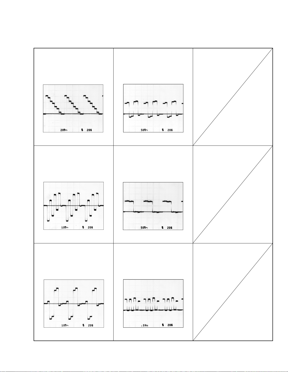
23
Page 24
PDP-502MX, PDP-502MXE
Synchronous Signal Processing Block 2
(INPUT4 PC siganl VESA:
1280x1024@60Hz (SXGA@60Hz)
when there is signal input [ separate H, V ]
CH1: K2025 (HD_4),
IC2005 Pin69 (HD input)
V : 5V/div H : 20msec/div
CH2: K2021 (HD_FIL), IC2005 Pin 107
V : 5V/div H : 20msec/div
CH3: K2019 (HD_u), IC2005 Pin 32
V : 5V/div H : 20msec/div
CH4: K2029 (HD_PLL), IC2005 Pin 118
V : 3.3V/div H : 20msec/div
YC_VY
(INPUT1 NTSC Color Bar)
CN104 Pin1
V : 20mV/div H : 20msec/div
R output
(INPUT3, 4 NTSC Color Bar Y/Cb/Cr)
IC306
V : 10mV/div H : 20msec/div
Synchronous Signal Processing Block 2
(INPUT4 PC siganl VESA:
1280x1024@60Hz (SXGA@60Hz)
when there is signal input [ separate H, V ]
CH1: K2021 (HD_FIL), IC2005 Pin 107
V : 5V/div H : 2.5msec/div
CH2: K2029 (HD_PLL), IC2005 Pin 118
V : 3.3V/div H : 2.5msec/div
CH3: K2432 (DIVOUT), IC2402 Pin 103
V : 5V/div H : 2.5msec/div
G output
(INPUT3, 4 NTSC Color Bar Y/Cb/Cr)
IC306
V : 20mV/div H : 20msec/div
B output
(INPUT3, 4 NTSC Color Bar Y/Cb/Cr)
IC306
V : 10mV/div H : 20msec/div
Y input
(INPUT1 NTSC Color Bar)
IC1201
V : 20mV/div H : 20msec/div
C input
(INPUT1 NTSC Color Bar)
IC1201
V : 20mV/div H : 20msec/div
24
Page 25
PDP-502MX, PDP-502MXE
INT_Y input
(INPUT1 NTSC Color Bar)
IC1401
V : 20mV/div H : 20msec/div
INT_Cb input
(INPUT1 NTSC Color Bar)
IC1401
V : 10mV/div H : 20msec/div
R input
(INPUT1 NTSC Color Bar)
IC1701
V : 50mV/div H : 20msec/div
G input
(INPUT1 NTSC Color Bar)
IC1701
V : 50mV/div H : 20msec/div
INT_Cr input
(INPUT1 NTSC Color Bar)
IC1401
V : 10mV/div H : 20msec/div
B input
(INPUT1 NTSC Color Bar)
IC1701
V : 50mV/div H : 20msec/div
25
Page 26

1
234
PDP-502MX, PDP-502MXE
3.4 SYNC SIGNAL PROCESSING BLOCK
A
B
Input from IC1201
(Jungle-IC)
in Comp/S input
(Positive polarity)
Separate HD/CS,
VD SYNC signal
input from BNC/Dsub 15p
Noise cancel processing
Countermeasure for copy guard
Limit to U-com processing velocity
(Max: 200kHz)
TC74VHC123
Control signal for switching
mask width (Lo : In PC input)
Noise cancel processing
Limit to U-com processing
velocity (Max: 200Hz)
HD/VD SYNC signal selected by input function
for generating Mask pulse
(except for when selecting HD_PLD, VD_PLD)
HD_PLD
VD_PLD
HD_3
HD_4
VD_3
VD_4
K2033
K2032
K2023
K2025
K2024
K2026
MASK_DSW
IC2004(2/2)
TC74VHC123
K2020
IC2004(2/2)
K2021
HD_MASK
VD_MASK
VD_FIL
HD_FIL
SYNC signal output
separated from Y/G
ON SYNC signal
SYNC CONTROL PLD
IC2005(PDY069)
Noise
Mask
Gate
Noise
Mask
Gate
SYNC signal selected based on
input function & HD/VD signal
detected (Unify the polarity to
negative polarity)
C
Y/G ON SYNC signal
in inputting Y colordifference or RGB
signals
D
Clamp & Blanking pulse
output to Analog Video
block
SYNC_SEPA
CLP_AMP
CLP_MAT
HBLK_MAT
VBLK_MAT
K2004
4pin
SYNC SEPA IC
IC2002
(M52346S)
K2012
K2015
K2013
K2014
14pin
15pin
13pin
6pin
8pin
2pin
1 pin
18pin
19pin
17pin
HD_+
HD_–
VD_+
HD_SEP
VD_SEP
Selected HD/VD signal
used for Separate input
SYNC signal detection
HSTATE
VSTATE
HPOL
VPOL
Information on detecting Separate
input SYNC signal & the polarity
CLP_SW1,2
CLP_SEP (Switching
Clamp pulse width
Clamp pulse generated by SYNC
Separate IC (Used in PC input)
CLP_SEPA
Signal
selector for
SYNC signal
Circuit for
switching
polarity
Decoding
HD/VD signal
detected
CONTROL
LOGIC
Selecting input
SYNC signal
Setting value of
HOLD Pulse width
CLAMP/
BLANKING
PULSE
CONTROL
&
20 bit /
Parallel
data
26
1234
Page 27

5
HOLD signal
generation circuit for
PLL control
Line
Number
Counter
HD Freq
Counter
67
PLL output HD for A/D sampling &
clock SYNC reference
K2432
K2029
HOLD controlling signal for comparing
K2030
K2408
Signal for detecting abnormal SYNC signal (Hi: in detecting)
Count value in the period of 1H by 16MHz clock (11-bit data)
Data is updated at the rate of HD1/8 dividing
K2019
K2018
PLL phase comparison.
PLL unlock information
(Hi: When PLL is not locked)
Vertical line number count value (11-bit data)
Data is updated every 1 V sync.
Timing signal for capturing horizontal frequency
count value (HD 1/8 dividing)
DIVOUT
HD_PLL
PLL input HD
HOLD_PLL
ULK_PLL
LINE(0:10)
SYNC STATE
H_COUNT(0:10)
HD_U
VD_U
8
PDP-502MX, PDP-502MXE
AMP/AD/PLL IC
IC2701
(CXA3106Q)
1_2CLK
XCLK
HD_DSEL
Signal Frequency DET
U-COM
IC2201
( PD2060A )
*Input signal detection
(stability)
*No signal input detection
*Detecting vertical frequency
*Controlling V_STD
(detecting frequency value)
A
B
SER-->PARA
CONV
5
Vertical SYNC signal for
input signal detection
Signal for detecting vertical frequency limit
Lo: Vertical frequency value is higher than
standard value (In PC input : fixed Hi)
Inverted PLL unlock information (Lo: When PLL is not locked)
Serial Control sig
PLD_CE
DATA
CLK
K2031
VD_DSEL
VD SYNC signal sent to Digital Assy
CLP1
CLP2
HBLK1
VBLK2
Clamp & Blanking signal output from
Digital Assy
K2027
V_STD
6
Serial data
REQ_Su
HOLD_Su
7
Sending
*Data of vertical frequency
*Data of horizontal frequency
*Data of total numbers of lines
*Information on inapplicable
frequency
U-COM ASSY
DIGITAL VIDEO ASSY
8
1_2CLK
XCLK
HD_DSEL
27
C
D
Page 28

1
0
C
E
S
E
234
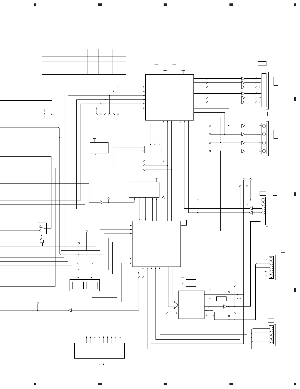
PDP-502MX, PDP-502MXE
3.5 DIGITAL VIDEO ASSY SECTION
D20
CN3403
A
A33
To VIDEO ASSY CN2901
D22
CN3405
B
1
A35
3
5
7
To VIDEO ASSY
CN2903
D17
A3
CN3402
5
8
9
10
11
12
8
8
8
8
8
8
XCLK
1_2CLK
HD
VD
ULK_PLL
CLP1
CLP2
HBLK1
VBLK1
V_STD
R (B)
G (B)
B (B)
R (A)
G (A)
B (A)
R (A)/G (A)/B (A)
IC3401, IC3402
R (B)/G (B)/B (B)
SGLB
TP3414
CLK_102
TP3411
CLK_101
TP3413
HD_IP
VD_IP
TP3410
IP PROCESSOR
+3.3V
IC1801
(PE5067A)
3
+3.3V
IC1901
(PE5066A)
I/F
Y (8bit)
Pb (8bit)
Pr (8bit)
RGB
≠
YPbPr
Sync CONT
CLAMP PULSE
GEN.
(IC#102)
5
+5V
IC2001
IP U-com.
IP
Process
Y (16bit)
Pb (16bit)
Pr (16bit)
Sharpness
Arrange
YPbPr
RGB
(IC#101)
≠
67
X Speed
X dencity
Y (8bit)
Pb (8bit)
Pr (8bit)
8bit × 2
RA_102
RB_102
GA_102
GB_102
BA_102
BB_102
HD_102
VD_102
TP2102
TP2103
DE_102
FLD_102
+3.3V
IC1951
(UPD4811650GF-A10)
16M SGRAM
+3.3V
IC1952
(UPD4811650GF-A10)
16M SGRAM
ASPECT
RATIO
CONV.
Sync
62M
+3.3V
Process
R
FIFO
W
IC2101
(PE5061A)
(IC#20)
+5V
(PD5538B)
Ser=Para
IC2251
OSD IC
WRITE CLK (SYSTEM CLK)
+3.3V
8bit × 2
RAI/RBI
GAI/GBI
BAI/BBI
7
H
V
FLD
VLD
6
RGB
MASK CONT
OSD MIX
CLK
OSD_H
+5V
OSD_V
IC2260
(PDY061A)
OSD
PROCESSOR
(PE5062A)
3
–1
γ
IC2151
6
ABL
R
G
B
BLK
2
To VIDEO ASSY CN2001
E6
C
D13
CN3273
4
5
6
7
8
9
From U-COM ASSY CN3606
D14
CN3271
1
E5
2
4
5
6
7
D
8
9
10
11
12
To U-COM ASSY CN3608
OSD_DATA1
OSD_CLK1
OSD_CE1
OSD_CLR1
SDATA1
SCLK1
PN_MUTEY
PN_MUTEX
PBUSY0
PERR0
IPBUSY0
IPERR0
RMT0
RESET_RET
D_CLK1
D_DATA1
PN_RST1
TP3408
TP3409
TP3407
TP3406
TP3405
X2001
20M
X2301
20M
+5V
67
PANEL U-com.
S2301
RST
IC2301
RST
+5V
IC2255
(MBM29F200BC-70PFTN-K)
FLASH ROM
5
TP2303
+5V
(LC3564BM)
G (IP ERR)
R (IP BUSY)
R (P BUSY)
G (STOP B)
IC2256
64k SRAM
RG
(P ERR)
D2306
D2302
+3.3V
(P
DRIVE
PATT
I
28
1234
Page 29

5
67
8
PDP-502MX, PDP-502MXE
EM CLK)
SK CONT
(PE5062A)
LK
SD_H
SD_V
2260
061A)
SD
ESSOR
205
–1
γ
ABL
IC2151
R
3
G
6
B
BLK
+3.3V
IC2201
(PE5064A)
DRIVE SEQUENCE
PATTERN GEN.
Dither
SYNC
CONT
X3201
62MHz
OSC
(IC#21)
D6
LUT
(IC#23)
VACANT
To Panel U-com
16bit × 2
VLD_A
VLD_B
FIELD
RA/RB
GA/GB
BA/BB
H
V
50M
25M
TP2154
TP2155
8
CD
25
8
24
3
X3202
50MHz
OSC
+3.3V
W
DATA
ARRANGE
R
DATA
CONVERT
CONT
IC2601
(PE5063A)
SUB FIELD
CONVERSION
W
DATA
ARRANGE
R
DATA
CONVERT
CONT
IC2701
(PE5063A)
SUB FIELD
CONVERSION
W
DATA
ARRANGE
R
DATA
CONVERT
CONT
(PE5063A)
SUB FIELD
CONVERSION
ADR/LBLK
MN (X Drive Gen. Pulse)
EF/GH/IJ (Y Drive Gen. Pulse)
1/2
SGRAM • READ OUT
MASTER CLOCK
(IC#22)
R
(IC#22)
G
(IC#22)
IC2801
B
+3.3V
IC2602
(HY58163210TQ-10)
16M SGRAM
+3.3V
IC2603
(HY58163210TQ-10)
16M SGRAM
+3.3V
IC2702
(HY58163210TQ-10)
16M SGRAM
+3.3V
IC2703
(HY58163210TQ-10)
16M SGRAM
+3.3V
IC2802
(HY58163210TQ-10)
16M SGRAM
+3.3V
IC2803
(HY58163210TQ-10)
16M SGRAM
IC3101
X DRIVE BUFFER
40
RDAT
40
GDAT
BDAT
40
XSUS-B/U/D/G
XPR, XR
ADR
BUFFER
IC2901–IC2910
IC3001–IC3010
IC3301–IC3304
IC3308, IC3309
IC3311, IC3312
D4
CN3256
A
B
To ADDRESS MODULE
C
F9
To X DRIVE ASSY
CN3402
TP553
+
Q554
IC551
REG
Q605
IC601
REG
TP601
+12V
)
6
+
2
Digital P.D.
CN551
D16
D555
TP555
+5V OVP
Q551
Q552
D605
Q601
Q602
TP604
+3.3V OVP
D556
TP556
+5V UVP
Q553
D606
+5V
TP603
+3.3V UVP
Q603
IC3102–IC3104
Y DRIVE BUFFER
+3.3V
YSUS-B/U/D/G
SI, MSK, CLK, PFS,
OE, YNR, YR
CN3252
D9
H1
D
To Y DRIVE ASSY
CN3751
29
5
6
7
8
Page 30

PDP-502MX, PDP-502MXE
Waveforms of DIGITAL VIDEO ASSY
Blanking waveform for analog use
CH1: TP3410 (HDIP)
CH2: TP3405 (CLP1)
CH3: TP3406 (CLP2)
CH4: TP3407 (HBLK1)
V : 5V/div H : 10msec/div
I-P V synchronous waveform
CH1: TP3411 (VD_IP)
CH2: IC1801 Pin 167 (Vi) –– IC1901 Pin 58
CH3: IC1901 Pin 56 (Vp) –– IC1801 Pin 169
CH4: IC1801 Pin 97 (VD_102)
V : 5V/div H : 2msec/div
I-P H synchronous waveform
CH1: TP3410 (HD_IP)
CH2: IC1801 Pin 168 (Hi) –– IC1901 Pin 57
CH3: IC1901 Pin 55 (Hp) –– IC1801 Pin 170
CH4: IC1801 Pin 98 (HD_102)
V : 5V/div H : 10msec/div
I-P clock waveform
CH1: IC1801 Pin 3 (CLK_102)
CH2: IC1901 Pin 239 (CLK_101)
V : 1V/div H : 5nsec/div
H synchronous waveform
TP2155
V : 1V/div H : 2msec/div
STOP B waveform
TP2205
V : 1V/div H : 2msec/div
I-P V synchronous waveform (enlarged)
CH1: TP3411 (VD_IP)
CH2: IC1801 Pin 167 (Vi) –– IC1901 Pin 58
CH3: IC1901 Pin 56 (Vp) –– IC1801 Pin 169
CH4: IC1801 Pin 97 (VD_102)
V : 5V/div H : 200msec/div
30
V synchronous waveform
TP2154
V : 1V/div H : 2msec/div
ADR resonant control signal waveform
CH1: IC3303 Pin11 (ADR_U)
CH2: IC3303 Pin12 (ADR_B)
CH3: IC3303 Pin13 (ADR_D)
V : 5V/div H : 1msec/div
Page 31

PDP-502MX, PDP-502MXE
Address resonant output waveform
IC2910 Pin 13
V : 1V/div H : 2msec/div
X drive waveform
CH1: IC3101 Pin 12 (XSUS_U)
CH2: IC3101 Pin 15 (XPR_U)
V : 0.5V/div H : 2msec/div
IC1801 HD input waveform
CN3404 Pin 29 (HD_IP), TP3410
V : 1V/div H : 10msec/div
GA input waveform
IC1801 Pin 31 (GA_IP (O))
V : 1V/div H : 0.1msec/div
IC1901 clock input waveform
CN3404 Pin 26 (CLK_101), TP3413
V : 1V/div H : 20nsec/div
VD input waveform
IC2101 Pin 236 (VD_102), TP2102
V : 1V/div H : 2msec/div
IC1801 VD input waveform
CN3404 Pin 30 (VD_IP), TP3411
V : 1V/div H : 2msec/div
GA output waveform
IC1801 Pin 121 (GA_102 (O))
V : 1V/div H : 0.1msec/div
HD input waveform
IC2101 Pin 235 (HD_102), TP2103
V : 1V/div H : 2msec/div
31
Page 32

PDP-502MX, PDP-502MXE
Address control signal
IC3304 Pin 11 (LBLK)
V : 1V/div H : 2msec/div
Address control signal
IC3308 Pin 15 (CLKDUI)
V : 1V/div H : 0.1msec/div
Address control signal
CN3275 Pin 26 (LEDUI)
V : 1V/div H : 0.5msec/div
32
Page 33

1
XSUS-B
R3435
IC3404
IC3404
R3424
IC3403
(TC74AC11F)
PDP Pulse Module
IC3402
(STK795-450)
+RESET BLOCK
LOGIC BLOCK
IC3408
(TC74AC08F)
IC3403
R3406
R3438
+5V
Q3406
Q3405
D3408
K3410
P.D. (X.C.P)
C3404
Q3404
Q3401–Q3403
11
XSUS-V
XSUS-D
XSUS-G
XPR-U
9
7
135
5
6
6
3
8
3
9
2
1
5
4
4
11
10
SUS-B
1
13
12
SUS-D
K3412
SUS-G
K3414
SUS-U
K3411
SUS-B
K3413
PR-U
K3409
2
+12V
7
5
3
+5V
+5V
VSUS
(175V)
1
+12V
XPD
367
5
VSUS
(175V)
1
SUS
GND
234
PD
DET.
12V
O. C DET.
SUS-U
21
26
29
40
20
18
14
16
1
175V
175V
0V
VSUS
(175V)
P-SUS (X)
SUS
GND
SUS
GND
SUS
GND
To
PANEL
24
VSUS/2
VSUS
SUSOUT
SUSGND
SUS-D
VDD
VCC
32
SUS-G
VSUS
SUS-G
SUS-U
SUS-B
SUS-D
175V
0V
R3410
R3411
D3403
D3402
t
t
X-PSUS
SUS
GND
VSUS
RP-U
F6
F5
F7
D4
From DIGITAL VIDEO Assy
E17
From U-COM Assy
E16
From U-COM Assy
PDP Pulse Module
IC3405
(STK795-450)
SUS-B
SUS-U
21
26
29
40
20
18
14
16
1
VSUS
(175V)
SUS
GND
SUS
GND
24
VSUS/2
VSUS
SUSOUT
SUSGND
SUS-D
VDD
VCC
32
SUS-G
3.6 X DRIVE ASSY SECTION
23
PDP-502MX, PDP-502MXE
4
A
B
1
C
2
3
D
33
4
Page 34

1
234
PDP-502MX, PDP-502MXE
3.7 Y DRIVE ASSY SECTION
HBLK1
TP3600
IC3607
IC5V
5
A
R3645
IC3602
IC3611
IC3610
IC3604
IC3609
IC3605
R3636
TP3608
PN_MUTEY
5
5
5
5
5
5
IC3613
(PDT043A)
2
3
4
5
7
8
PLD & MUTE
9
6
11
MUTE
14
15
16
17
18
13
12
19
SUS-B
SUS-U
SUS-D
SUS-G
YCP-MSK
YSUS-MSK
OFS
YNR-D
VH
IC5V
PSUS
SI DATA
IC3601
(TC74ACT541FT)
13
14
15
16
17
12
11
18
SCAN (A) ASSY
(UPPER)
SCAN (B) ASSY
(LOWER)
H2
H3
SUS-B
TP3703
SUS-U
TP3704
SUS-G
SUS-D
TP3705
TP3706
SI
TP3604
SCAN BLOCK
CLK
TP3601
IC3600
R3602
CN3605
B
D8
From DIGITAL VIDEO ASSY
PN_MUTEY
HBLK1
CLK
LE_S
CLR
HBLK2
LBLK
YSUS-B
YSUS-U
YSUS-D
YSUS-G
YNR-D
YNR-U
SUS-MSK
CP-MSK
OFS
H1
44
42
SI
40
38
36
34
32
30
28
R3619
26
24
22
20
18
16
14
6
R3654
R3655
(TC74VHC541FT)
4
5
6
7
8
9
R3603
IC3606
(TC74VHC541FT)
R3614
(TC74VHC541FT)
2
3
7
IC3614
2
3
4
5
6
7
8
9
18
17
13
16
15
14
13
12
11
HBLK2
TP3606
TP3603
LBLK
18
17
16
15
14
13
12
11
TP3605
IC3612
IC3612
LE
CLR
TP3602
C
E8
From U-COM ASSY
E7
From U-COM ASSY
D
CN3701
+5V
+12V
DRV PD
YDC_DC. PD
+14V
–8V
VSUS
SUS GND
VSUS
+10V
CN3700
H5
H4
1
3
7
8
5
6
1
4
6
VSUS
175V
SUS
GND
D853
D758
D761
D709
D710
D811
D814
TP853
IC5V OVP
TP752
VH OVP
TP754
VH UVP
TP706
VOFS OVP
TP707
VOFS UVP
TP802
VRN OVP
TP804
VRN UVP
Q802
Q750
Q752
Q700
Q800
–8V
IC5V, VF
14V
DC–DC CONV.
IC850, IC851
T850
VSUS
VH DC–DC
CONV.
IC750, IC751
T750
VSUS
SUS GND
VOFS
DC–DC CONV.
IC701, IC702
T700
DC–DC CONVERT BLOCK
D890
TP855 TP856
VFZ+
+
VFZ–
IC5V
+
TP851
VH
D753
+
PSUS
D802
TP751
TP753
D700
TP800
TP803
VRN
(–200V)
+
TP3707
VOFS
TP705
SUS
GND
OFS
+
SUS
GND
R3766
IC3710
TP702
IC3711
VRN
+ 5V
REG.
5
OFS BLOCK
VOFS
7
5
IC3712
R3768
R3769
R3772
R3773
R3774
Q3714
Q3716
34
1234
Page 35

5
67
8
PDP-502MX, PDP-502MXE
+5V For
Logic Block
Q3701
+12V
O. C DET.
PD
DET.
R3708
R3710
R3700
Q3703
SUSTAIN BLOCK
PDP Pulse Module
(STK795-450)
VCC
16
SUS-B
20
SUS-U
VDD
18
SUS-D
14
SUS-G
PDP Pulse Module
(STK795-450)
VCC
16
SUS-B
20
SUS-U
VDD
18
SUS-D
14
SUS-G
IC3702
IC3707
VSUS
SUSOUT
VSUS/2
SUSGND
VSUS
SUSOUT
VSUS/2
SUSGND
VSUS
(175V)
1
40
26
21
24
32
SUS
GND
VSUS
(175V)
1
40
26
21
24
32
SUS
GND
175V
0V
175V
A
SUS
GND
B
0V
SUS
GND
R3768
R3769
R3772
R3773
R3774
Q3714
Q3716
IC3713
R3781
7
2
5
4
R3788
Q3721
D3720
–RESET BLOCK
YSUS-MSK
SUS
GND
R3712
D3714
R3776
R3777
R3709
VCP BLOCK
D3713
Q3719
R3784
R3705
D3717
Q3704
D3700
I
VCP
IC3700
+ 5V
REG.
G
TP3700
VCP
O
IC3703
5
R3714
IC3701
R3734
18
17
16
15
14
13
12
11
D3709
IC3706
7
5
7
5
IC3708
R3794
R3794
R3795
R3795
Q3709
Q3710
IC3704
Q3708
Q3711
7
5
R3796
7
5
IC3709
R3793
R3793
R3796
Q3706
Q3712
K3716
PSUS
Q3705
Q3713
C
D
PSUS
To SCAN MODULE
Copper Plate
SUSTAIN MASK BLOCK
35
5
6
7
8
Page 36

PDP-502MX, PDP-502MXE
Waveforms of X DRIVE Assy, Y DRIVE Assy and SCAN MODULE
Sustained waveform
CH1: P.SUS TP3716 (P.SUS) – TP3713 (SUS.GND)
CH2: YSUS-B TP3703 (YSUS-B) – TP3609 (D.GND)
CH3: YSUS-U TP3704 (YSUS_U) – TP3609 (D.GND)
CH4: YSUS-D TP3705 (YSUS_D) – TP3609 (D.GND)
CH5: YSUS-G TP3706 (YSUS-G) – TP3609 (D.GND)
CH1
CH2
CH3
CH4
CH5
V: 50V/div., H: 500nsec/div.
V: 10V/div., H: 500nsec/div.
V: 10V/div., H: 500nsec/div.
V: 10V/div., H: 500nsec/div.
V: 10V/div., H: 500nsec/div.
–GND
–GND
–GND
–GND
–GND
Sustained waveform (1 field)
CH1: X drive waveform
CH2: Y drive waveform
K3402 (P. SUS) – K3404 (SUS. GND)
V: 50V/div., H: 2msec/div.
TP3716 (P. SUS) – TP3713 (SUS. GND)
V: 50V/div., H: 2msec/div.
Sustained waveform (1st sub-field)
CH1: X drive waveform
CH2: Y drive waveform
CH1
CH2
K3402 (P. SUS) – K3404 (SUS. GND)
V: 50V/div., H: 200µsec/div.
TP3716 (P.SUS) – TP3713 (SUS.GND)
V: 50V/div., H: 200µsec/div.
Reset Pulse
Portion
Sustained
Portion
Sustained waveform
(reset pulse portion; enlarged)
CH1: X drive waveform
CH2: Y drive waveform
K3402 (P. SUS) – K3404 (SUS. GND)
V: 50V/div., H: 20µsec/div.
TP3716 (P. SUS) – TP3713 (SUS. GND)
V: 50V/div., H: 20µsec/div.
Sustained waveform
(portion where sustaining was ended; enlarged)
CH1: X drive waveform
K3402 (P. SUS) – K3404 (SUS. GND)
V: 50V/div., H: 5µsec/div.
CH2: Y drive waveform
TP3716 (P. SUS) – TP3713 (SUS. GND)
V: 50V/div., H: 5µsec/div.
CH1
–GND
CH2
–GND
Control waveforms
for additional pulses (1 field)
CH1: Y drive waveform
TP3716 (P.SUS) – TP3713 (SUS.GND)
V: 100V/div., H: 2msec/div.
CH2: CP_MSK
IC3601 Pin17 (CP_MSK) – TP3609 (D.GND)
V: 10V/div., H: 2msec/div.
CH3: SUS_MSK
IC3601 Pin12 (YSUS_MSK) – TP3609 (D.GND)
V: 10V/div., H: 2msec/div.
CH4: OFS TP3707 (OFS) – TP3609 (D.GND)
V: 10V/div., H: 2msec/div.
–GND
–GND
CH1
CH2
Sustained waveform
CH1: X drive waveform
K3402 (P. SUS) – K3404 (SUS. GND)
V: 50V/div., H: 2µsec/div.
CH2: Y drive waveform
TP3716 (P. SUS) – TP3713 (SUS. GND)
V: 50V/div., H: 2µsec/div
CH1
CH2
(1 field; enlarged)
CH1
–GND
CH2
–GND
Sustained waveform
(portion where sustaining was started; enlarged)
CH1: X drive waveform
K3402 (P. SUS) – K3404 (SUS. GND)
V : 50V/div., H : 5µsec/div.
CH2: Y drive waveform
TP3716 (P. SUS) – TP3713 (SUS. GND)
V : 50V/div., H : 5µsec/div.
CH1
–GND
CH2
–GND
CH1
–GND
CH2
CH3
–GND
CH4
Control waveforms
for additional pulses
(1 sub-field; enlarged)
CH1: Y drive waveform
TP3716 (P.SUS) – TP3713 (SUS.GND)
V: 50V/div., H: 200µsec/div.
CH2: CP_MSK
IC3601 Pin17 (CP_MSK) – TP3609 (D.GND)
V: 10V/div., H: 200µsec/div.
CH3: SUS_MSK
IC3601 Pin12 (YSUS_MSK) – TP3609 (D.GND)
V: 10V/div., H: 200µsec/div.
CH4: OFS TP3707 (OFS) – TP3609 (D.GND)
V: 10V/div., H: 200µsec/div.
–GND
CH1
CH2
–GND
CH3
CH4
–GND
–GND
–GND
–GND
–GND
–GND
–GND
–GND
36
Page 37

PDP-502MX, PDP-502MXE
SCAN IC
control waveform (1 sub-field)
CH1: Y drive waveform
TP3716 (P.SUS) – TP3713 (SUS.GND)
V: 50V/div., H: 200µsec/div.
CH2: SI TP3604 (SI) – TP3609 (D.GND)
CH3: CLK TP3601 (CLK) – TP3609 (D.GND)
CH4: LBLK TP3603 (LBLK) – TP3609 (D.GND)
V: 10V/div., H: 200µsec/div.
CH1
CH2
CH3
CH4
SCAN IC
control waveforms (enlarged)
–GND
–GND
–GND
–GND
CH1: Y drive waveform
TP3716 (P.SUS) – TP3713 (SUS.GND)
V: 50V/div., H: 5µsec/div.
CH2: SI TP3604 (SI) – TP3609 (D.GND)
CH3: CLK TP3601 (CLK) – TP3609 (D.GND)
CH4: LBLK TP3603 (LBLK) – TP3609 (D.GND)
V: 10V/div., H: 5µsec/div.
Y-drive sustained waveforms
(for 1 field)
CH1: SCAN output waveform
SCAN IC output – TP3713 (SUS.GND)
V: 50V/div., H: 2msec/div.
CH2: Y drive waveform
TP3716 (P.SUS) – TP3713 (SUS.GND)
V: 50V/div., H: 2msec/div.
CH1
CH2
Sustained waveforms
(selected pulse portions of waveforms; enlarged)
CH1: SCAN output waveform
SCAN output – TP3713 (SUS. GND)
V: 50V/div., H: 10µsec/div.
CH2: Y drive waveform
TP3716 (P.SUS) – TP3713 (SUS.GND)
V: 50V/div., H: 10µsec/div.
Sustained waveforms
(selected pulse portions of waveforms; 1 sub-field)
CH1: Y drive waveform
TP3844 – TP3713 (SUS.GND)
CH2: Y drive waveform
TP3837 – TP3713 (SUS.GND)
CH3: X drive waveform
K3402 (P.SUS) – K3404 (SUS.GND)
V: 50V/div., H: 200µsec/div.
–GND
CH1
CH2
–GND
CH3
Sustained waveforms
(selected pulse portions of waveforms; 1 sub-field)
(enlarged)
CH1: Y drive waveform
TP3844 – TP3713 (SUS.GND)
CH2: Y drive waveform
TP3837 – TP3713 (SUS.GND)
CH3: X drive waveform
K3402 (P.SUS) – K3404 (SUS.GND)
V: 50V/div., H: 20µsec/div.
–GND
–GND
–GND
CH1
CH2
CH3
CH4
Waveforms of CABLE Assy
Address resonant output waveform
(TP 1001) and midpoint voltage (C1001)
(VIDEO input, black display)
1
Field rate V: 2V/div H: 2msec/div
2
Resonant pulse rate
1
2
V: 2V/div H: 500nsec/div
–GND
–GND
–GND
–GND
–GND
CH1
CH2
–GND
–GND
Address resonant control signal waveform
(VIDEO input, black display; resonant pulse rate)
CH1: ADR-U (IC1007 Pin 2) V : 2V/div H : 500nsec/div
CH2: ADR-B (IC1007 Pin 4) V : 2V/div H : 500nsec/div
CH3: ADR-D (IC1010 Pin 1) V : 2V/div H : 500nsec/div
CH4: ADR-G (IC1009 Pin 1) V : 2V/div H : 500nsec/div
CH1
CH2
CH3
–GND
–GND
–GND
CH1
CH2
CH3
–GND
–GND
–GND
–GND
CH4
–GND
37
Page 38

1
234
PDP-502MX, PDP-502MXE
3.8 U-COM ASSY SECTION
A
B
CCD/TELTEXT
VIDEO ASSYVIDEO ASSY
3D Y/C SEPA.
M35070 (35071)
PD0264AM-TFB
(PDP-505HD Only)
E2PROM
24LC01B
Jungle IC
TB1227BN
MATRIX IC
CXA2101
TPU3050
EXPANDER
CXA1875AM
LSI
uPD64081B
OSD IC
OSD IC
SCL
SDA
∗OSD_CLR
∗OSD_CE
OSD_H
2
3
SYSTEM
CONTROL
u-COM.
IC3604
(M38869FFAHP)
63
53
64
54
PM_ST
80
∗GRN
37
∗RED
38
39
∗YLW
KEY (MONITOR)
23
MR_KEY (SYSTEM)
REMSW
68
REM
22
∗CB_MUTE
67
20
TXD
21
RXD
32
RTS
14
CTS
Hi
REM_MP
Lo
∗KEY
MR_KEY
REM_PM
(SYSTEM)
REM
(MONITOR)
REM
RXD/CB OUT
RXD
M.R. (C.B.)
CONNECTION
DETECT CIRCUIT
LED
DRIVE/CONTROL
CIRCUIT
KEY SCAN uCOM.
PD5136
MEDIA
RECEIVER
REMOTE CONTROL
RECEIVER
CIRCUIT
REMOTE CONTROL
SIGNAL
CONTROL CIRCUIT
RS-232C
CONTROLLER
TC74HC00AF
RS-232C
DRIVER/RECEIVER
MC145407F
IR
RECEIVE
ASSY
CONTROL
ASSY
U-COM
ASSY
C
VIDEO ASSY DIGITAL VIDEO ASSYDIGITAL VIDEO ASSY
D
U-COM
ASSY
PLD
PE9006B
PLL
CXA3106A
SERIAL
CLK/DATA
CONTROLLER
TC74VHC02FT-TBB
PANEL u-COM
HD64F3067
IP u-COM
HD64F3067
RESET IC
PST9146N
RESET IC
PST9146N
SYNC u-COM
HD64F3067
POWER SUPPLY
ASSY
STB 5V
RESET IC
PST9146N
∗PLD_CE
∗PLL_CE
SC_DT
(ULK_PLL)
∗PN_CE
CLK2
DATA2
D_CLK
D_DATA
RESET_RET RST_RET
RESET_SU
∗POWER
PN BUSY
PN ERR
RMT
IP BUSY
IP ERR
RST_SU
VPOL_U
∗SU_CE
I_DET
DTO_SU
REQ_SU
PLK_ID
POWER
∗RST
VOL
56
52
31
10
59
60
62
∗A_MUTE1
∗A_MUTE2
A_MUTE3
0–5V DC
AUDIO PRE-AMP
IC
AUDIO
CIRCUIT
AUDIO AMP ASSY U-COM ASSY U-COM ASSYVIDEO ASSY
7
DATA2
51
7
8
5
34
33
41
42
11
16
43
57
40
9
15
69
26
25
8
58
44
1
4
∗PN_MUTEX
47
48
∗PN_MUTEY
S_D
74
TEMP2
75
TEMP
76
FAN_MAX
61
∗PN_RST
35
(E) SCL
45
EP_RST
17
46
CLK2
∗ZOOM_CE
V_MUTE
S2_DET
Y_DETI
(E) SDA
FULL AUTO
ZOOM IC
HG62G010R29FB
RGB AMP IC
M52337SP
S2 DETECT
CIRCUIT
Y SIGNAL
DETECT
CIRCUIT
X DRIVE
PLD
Y DRIVE
PLD
FAN CONTROL
BLOCK
RESET
MATRIX IC
TC7W08FU
2
PROM
64k E
24LC64
U-COM
ASSY
X DRIVE
ASSY
Y DRIVE
ASSY
UCOM
ASSY
DIGITAL
VIDEO
ASSY
U-COM
ASSY
38
1234
Page 39

Waveforms of U-COM ASSY
PDP-502MX, PDP-502MXE
IC3602-pin4
(Clock input: X3602)
V : 1V/div H : 1msec/div
1
2
IC3602-pin19
(Key code output)
V :2V/div H : 100msec/div
IC3602-pin19 (enlarged)
(Key code output)
V :2V/div H : 10msec/div
IC3604-pin7 (CLK2)
51
V :2V/div H : 50msec/div
IC3604-pin7 (CLK2)(enlarged)
V :2V/div H : 20msec/div
IC3604-pin8 (DATA2)
6
V :2V/div H : 50msec/div
IC3604-pin8 (CLK2)(enlarged)
V :2V/div H : 20msec/div
5
6
5
enlarged
6
IC3604-pin45 ((E)SCL)
8
V :2V/div H : 200msec/div
IC3604-pin45 ((E)SCL)(enlarged)
V :2V/div H : 50msec/div
9
IC3604-pin46 ((E)SDA)
V :2V/div H : 200msec/div
IC3604-pin46 ((E)SDA)(enlarged)
V :2V/div H : 50msec/div
–GND
–GND
–GND
–GND
IC3604-pin28
11
(Clock input: X3601)
V :2V/div H : 50nsec/div
-
10MHz
IC3612-pin10 (D_CLK)
13
V :2V/div H : 100msec/div
IC3612-pin10 (D_CLK)(enlarged)
V :2V/div H : 20msec/div
IC3612-pin13 (D_DATA)
13
V :2V/div H : 100msec/div
IC3612-pin13 (D_DATA)(enlarged)
V :2V/div H : 20msec/div
2
enlarged
IC3604-pin2 (SCL)
3
V :5V/div H : 50msec/div
IC3604-pin3 (SDA)
4
V :5V/div H : 50msec/div
3
4
–GND
–GND
8
9
8
enlarged
9
IC3604-pin23 (KEY)
10
V :2V/div H : 100msec/div
IC3604-pin23 (KEY)(enlarged)
V :2V/div H : 10msec/div
-
enlarged
–GND
–GND
–GND
–GND
–GND
–GND
=
~
=
enlarged
~
–GND
–GND
–GND
–GND
39
Page 40

PDP-502MX, PDP-502MXE
Pin Function
Pin
Name Function
No.
1 S2_DET S2 Signal detection 0–1.3V: Normal, 1.4–2.4V: Letter Box, 2.5–5V: Squeeze I ––
OPTION Option Video Box detection High: non existence, Low: existence of Video Box I –– ––
2 SCL I2C-BUS Clock 0–5V clock signal: always communicating when power on O
3 SDA I2C-BUS Data 0–5V clock signal: always communicating when power on I/O
4 V_DETI Result of Y signal detection High: Y Signal detected, Low: Y Signal not detected I
5 PN_BUSY BUSY signal from Panel U-Com High: In exchanging input functions, Low: Normal I
6 ––––– No allocation(not used)
7 CLK2 Clock output for Serial 3 lines 0–5V clock signal: always communicating when power on O
8 DATA2 Data output for Serial 3 lines 0–5V serial signal: always communicating when power on O
9 DTO_SU Serial data input from SYNC u-com High: Normal, 0–5V serial signal: During communication I
10 VOL Audio volume output PWM output O ––
11 RST RET Reset Signal from Digital Video Assy High: Normal, Low: In Reset I
(Panel u-com and IP u-com)
12 ––––– No allocation (not used)
13 ––––– No allocation (not used)
14 CTS Not used
15 REQ_SU Request to read detected frequency from High: Normal, Low: In requesting I
SYNC u-com
16 RST_SU Reset Signal from SYNC u-com High: Normal, Low: In resetting I
17 EP_RST Reset output to E2PROM High: In resetting, Low: Normal O
18 BUSY2 Not used
19 SCL2 Not used
20 TXD RS-232C sending data 0–5V serial signal O
21 RXD RS-232C receiving data 0–5V serial signal I
22 REM Remote Control unit signal input High: Normal, 0–5V serial signal: In input from Remote I
23 KEY Key Matrix, Key of the unit input High: Normal, 0–5V serial signal: In Key input I
24 CNVSS Controlling operation mode of u-com of Low: Normal I
25 *RST Reset input High: Normal, Low: In Reset I
26 POWER Power on/off High: When power on, Low: In Stand-by O
27 ––––– No allocation (not used)
28 X_IN Clock input 10 MHz sine wave I
29 X_OUT Clock output 10 MHz sine wave O
30 VSS Power supply terminal STB GND I
31 SC_DT
(ULK_PLL)
32 RTS Not used
33 RMT Signal of request to quit sending Low: Normal I
34 PN_ERR
35 *PN_RST
36 ––––– No allocation (not used)
37 *GRN Green LED lighting Low: In lighting Green LED O
38 *RED Red LED lighting Low: In lighting Red LED O
the unit
Detecting SYNC Signal output from Analog
Assy to Digital Assy
commands from Panel u-com
Communication error signal from Panel u-com
Reset signal output to Panel u-com & IP u-com
(both-way communication with Full Auto Zoom IC )
Control unit
High: existence of Sync signal, Low: non existence I
Low: Normal I
High: Normal, Low: In Reset O
Operation of Terminals (during power on)
I/O
PDP-
502MX
PDP-
502MXE
PDP-
505HD
40
Page 41

PDP-502MX, PDP-502MXE
Pin
Name Function
No.
39 *YLW Yellow LED lighting Low: In lighting Yellow LED O
40 I_DET Not used
41 IP_BUSY BUSY signal from IP u-com High: At the timing of VD SYNC I
42 IP_ERR
43 VPOL_U Not used
44 V_MUTE Analog video mute output High: When muting, Low: Normal O
45 (E) SCL I2C-BUS Clock for E2PROM
46 (E) SDA I2C-BUS Data for E2PROM
47
*PN_MUTEX
48
*PN_MUTEY
49 *V_STDO Not used
50 STDSW Not used
51 *PN_CE Chip Enable for Panel u-com & IP u-com High: Normal, Low: During communication O
52 *PLL_CE Chip Enable for PLL IC High: Normal, Low: During communication O
53 *OSD_CE Chip Enable for OSD IC High: Normal, Low: During communication O –– ––
54 HPOL_U Not used
55 PGM_OE Not used
56 *PLD_CE Chip Enable for PLD (Analog Video Assy) High: Normal, Low: During communication O
57 *SU_CE Chip Enable for SYNC u-com High: Normal, Low: During communication O
58 *ZOOM_CE Chip Enable for Full Auto Zoom IC High: Normal, Low: During communication O –– ––
59 *A_MUTE1 Audio Mute 1 High: Normal, Low: When muting O ––
60 *A_MUTE2 Audio Mute 2 Muting audio out High: Normal, Low: When muting O ––
61 FAN_MAX Command to rotate Fan with max. speed High: In setting Fan max. speed, Low: Normal O
62 A_MUTE3 Audio Mute 3 Mute in suspending High: When muting, Low: Normal O ––
63 *OSD_CLR Reset signal output to OSD IC High: Normal, Low: In resetting O ––
64 OSD_H OSD Timing Pulse for SYNC processing Pulse input I –– ––
65 ––––– No allocation (Not used)
66 DRV_OFF Not used
67 *CB_MUTE Combination Mute High: When ID is set, Low: Normal O ––
68 REMSW Not used
69 PLK_ID Not used
70 ––––– No allocation (not used)
71 VCC Power source input STB +5V I
72 VREF Reference voltage input of AD/DA Converters STB +5V I
73 AVSS Analog power input of AD/DA Converters STBGND I
74 S_D Shut down detection for high temperature High: In high temperature, Low: Normal I
75 TEMP2 Not used
76 TEMP
77 ––––– No allocation (Not used)
78 ––––– No allocation (Not used)
79 ––––– No allocation (Not used)
80 PM_ST Not used
Communication error signal from IP u-com
X Drive Panel mute output High: Normal, Low: When muting O
Y Drive Panel mute output Fixed "High" O
Temperature detection for On screen bar display
Operation of Terminals (during power on)
Low: Normal I
High: Normal, 0–5V clock signal: During communication
High: Normal, 0–5V serial signal: During communication
(Approx.80ms interval)
(Approx.80ms interval)
0–5V DC value I
I/O
I/O
I/O
PDP-
502MX
PDP-
502MXE
PDP-
505HD
41
Page 42

1
234
PDP-502MX, PDP-502MXE
3.9 MAIN POWER ASSY SECTION
2
D150
R189
In rush R
R133
R134
R168
Q185
R190
D185
AC OFF DET
+B (380V)
+
C202
DRV
ON/OFF
Q437
TP131
Lo V VADR
MUTE
D190
VADR VSUS
SEQUENCE
R184
Q186
D186
D191
SEQUENCE
R185
Q183
D183
DRV
&
UVP
Q439
D189
D188
Mute
RCC CONT
+B
Q301
SW Tr
(2SK2847)
R312
RCC CONT
+B
R232
R316
R347
Q352
Comp
R253
7
Comp
Error
AMP
1
R363
RCC CONT
4
4
Trig (-V)
SW Tr
(2SK2847)
Q201
SW Tr
(2SK2847)
5
3
2
1
Error
AMP
5
3
2
1
2
3
Q351
4
5
R140
R166
Q131
+B
D402
ON /OFF
SW103
1
3
R167
R131
R132
D131
Q136
POWER FACTOR CONTROL
L133
R139
1
3
+B Adj
VR131
IC131
Power
Factor
Correction
8
7
6
5
R165
R154
R155
AEK1071
A
FU101
1
2
RY101
D132
Q132
D151
1
4
Q134
D138
+B OVP
B
P.ON:Lo
T111
ATK1133
3
D111
4
IC111
2
SW
IC
C
STBY
POWER
D112
D113
+
5
3
4
TRANS
IC112
3
4
D116
STBY
2
1
TP112
D461
D401
Q401
Q402
D118
D117
R121
R122
SW111
AC100V (PDP-502MX)
AC200V (PDP-502MXE)
Q111
R123
D459
IC113
VR111
+5V Adj
D458
D115
R113
TP111
STB+5V
D457
POWER
P.OFF:Hi P.ON:Lo
STB+5V
D433
Audio
Digital PD
D447
RY131
14V
STB +12V
POWER Down Detection Block
D441
X DRV
PD
D446
D
1 3
P1
To U-COM
ASSY
1
4
D463R406
D439
Y DCDC
PD
D445
IC181
R426
2
D437
Y DRV
PD
D406
AC200V
PD
3
R156
D407
Main PWR
PD
R415
IC401
PFC STOP
DET
14V
D405
D408
Q425
R410
PFC STOP PD
UVP PD
OVP
POWER
D412
Q406
+
R364
R385
Q407
7
Comp
Error
AMP
1
STB +12V
UVP
MUTE
at P.ON
Q408
D413
D414
42
1234
Page 43

5
67
8
PDP-502MX, PDP-502MXE
4
p
Trig (-V)
SW Tr
(2SK2847)
C CONT
R364
R385
Q407
Q201
SW Tr
(2SK2847)
5
3
2
1
Error
AMP
5
3
2
1
2
3
Q351
4
7
Comp
Error
AMP
1
STB +12V
UVP
MUTE
at P.ON
Q408
D413
D414
5
1
2
3
2
1
2
3
R424
3
4
T202
ATK1128
VSUS TRANS
T201
ATK1128
VSUS TRANS
IC201
3
4
T301
ATK1129
VADR TRANS
IC301
3
4
T351
ATK1130
IC351
1
Trig
(-V)
14V
R436
R437
VADR
D205
R440
R441
VADR
Q415
OVP
OVP
TP201
(170V)
VSUS+10V
D422
14V
UP
Q417
D428
D434
R443
-8V
8V
14V
UVP
OVP
VSUS
TP301
VADR
(60V)
TP351
-8V
SUS
GND
ADR
GND
Q419
14V OVP
P5
1
2
4
6
7
8
A.GND
TP352
+8V
TP355
+14V
D.GND
D431
To UCOM ASSY
-8V
14V
12V
R444
R493
14V
-8V
1
2
3
4
D.GND
8V
P6
12
11
7
6
5
2
1
6
1
11
P4
TP353
+12V
12V
To ANALOG VIDEO ASSY
To UCOM ASSY
10
9
7
14V
5
3
To UCOM ASSY
2
1
P3
A
B
C
D
VSUS Discharging R
R228 R227 R226 R262 R263 R264
170V
+
1 3 5
One Shot
IC204
OTL CONT
(A) ASSY
IC202
D206
R315
1 3 5
One Shot
IC304
OTL CONT
(B) ASSY
IC302
Q354
D202
+
D.GND
1 3 5
One Shot
IC354
OTL CONT
(C) ASSY
D355
14V up
VR356
14V Adj
R206
Mute
DisCharge
Q207, Q206
Q205,
+
12V
UVP
R356
VR201
VSUS
Adj
R210
R306
R348
VR301
VADR
Adj
Vadr up
R447
Q421
Q420
R463
R461
R462
UVP MUTE
D305
8V UVP
R445
R358
R360
IC403
Q212
Q213
D451
R268
VSUS
VADR
UVP
Q304
12V
D453
IC352
R357
6
5
UVP
Q202
10V
SUS
GND
R208
2
1
60V
ADR
GND
2
1
12V
-8V
8V
14V
2
D356
UVP
Q302
D302
D373
D352
IC405
Q422
R358
7
R451
UVP
D213 D212
Q416
D427
Q416
IC404
D432
Q435
-8V UVP
14V
D421
D449
R491R490
IC402
VSUS
UP
14V
D429
43
5
6
7
8
Page 44

1
TEMP SENS
IC4101
REG
VIN
Vo
Vad
IC3952
PQ20VZIU
FAN
AXM1036
+
–
IC3954
SENS A
3
10VREG
1
1
E27
LM50CIM3-TLB
SENSOR (A) ASSY
AWZ6501
K3952
SENS A
2
1
2
3
R4151
D3952
IC3953
From Power
Supply assy
0.7V DC GENE
FAN MAX CONT
Q3959
Q3960
REG
VIN
Vo
Vad
IC3956
PQ20VZIU
+
–
+
–
1
1
4
4
3
3
7
+14V
P1
E2
R3971
+10V
REG
IC3951
PQ20VZIU
1
3
4.5V DC
FAN MIN
VOL GENE
10V REG
61
Q3966
IC3604
SYSTEM
CONT U-COM
Q3962
D3953
Q3957
Q3951
Q3952
Q3953
Q3954
D3951
+14V_FAN1
Q3958
FAN MAX
ShutDown
TEMP SENS
76
D3959
5
7
6
IC3954
K3954
SD
U-COM ASSY
AWZ6499 (PDP-502MX)
AWZ6520 (PDP-502MXE)
ENV.
TEMP
MIN
30.0
43.0
45.0
50 (S.D)
IC3954
Pin1 Out
4.45V
5.22V
5.55V
6.46V
FAN
DRV TP
6.04V
6.08V
13.28V
16.58V
STOP
MIN
30degC
45degC
(MAX)
FAN SPEED
S.D = Caution display for 30 sec.
6.5VDC
S.D DET
K3951
FAN DRV
FAN
AXM1036
FAN
AXM1036
FAN
AXM1036
PDP-502MX, PDP-502MXE
3.10 FAN CONTROL SECTION
A
234
B
C
D
44
1234
Page 45

PDP-502MX, PDP-502MXE
45
Page 46

PDP-502MX, PDP-502MXE
6. ADJUSTMENT
SERVICE FACTORY MODE
Perform the operations of Service factory mode using the remote control unit provided with thePDP-501HD
(CU-PD001: AXD1432) or the remote control unit provided with the PDP-502HD (CU-PDP009: AXD1673).
Entering Service Factory Mode
POWER
MENU
SET
POWER
CU-PDP001
(AXD1432)
MUTE
SOUND
VOLUME
Normal Operation Mode
(Standby)
"Menu" key
∗
Service Factory Mode
SERVICE mode
RANGE CHECK mode
"MUTE"
key
PICUTRE mode
REFERENCE 1…… "1" key
REFERENCE 2…… "2" key
VIDEO BOX ……… "3" key
"Menu" key
‘
∗
"Menu" key
‘
"Set" key
‘
"Power" key
∗
CU-PDP009 has two "Power" keys. In Service factory Mode, use
the "Power" key located on the upper left of the remote control unit.
"MUTE" key
"MUTE" key
"MUTE" key
within
3 seconds
(refer to Technical Manual)
Displaying version of the system micro computer.
Displaying type and format of detected input signal.
Displaying the frequency/the number of lines of
input signal.
Mode for checking operations of each device at
video section, by changing its adjustment value to
maximum and to minimum.
This mode is not used for repair service.
"1" and "2" keys:
Mode for adjusting video section (Independent for
each signal type and format)
"3" key:
Mode for adjusting video box (PDA-5001)
(PDP-502MXE only)
"Power" key
Integrator Mode
within
3 seconds
46
MUTE
MENU
SET
CU-PDP009
(AXD1673)
SOUND
VOLUME
INITIALIZE mode
SUB VIDEO…………
"1" key + "SET" key
DRIVE ADJ…………
"9" key + "SET" key
Mode for each setting
Drive section adjustment
Pulse/ABL adjustment
Sub video section adjustment
(Common value to all input signal)
In each adjustment mode, adjusted values can be changed with +/– of "SOUND VOLUME"
key on the remote control unit.
After adjustment, adjusted values can be fixed by pressing "SET" key.
Note)
When an input signal mode is changed, the adjustment mode is set to Normal operation mode
automatically.
SETTING (PC/VIDEO) and SIGNAL (RGB/COMPONENT) can not be changed in the
service factory mode.
When entering Service factory mode, all items of PICTURE adjustment in Normal menu/
Integrator mode and all items of SCREEN menu (such as position adj.), except for CLK
Phase, are reset to their initial value.
Page 47

SERVICE MODE
Version of the system micro computer
PD5621–
PD5622–∗∗ (502MXE)
∗∗
PDP-502MX, PDP-502MXE
(502MX)
Signal mode discrimination of current input signal
PD5531–01 MODE 06–A/N
FH : 15.7KHZ
FV : 60.0 HZ
LINE: 480LINE
Current input signal’s Horizontal frequency
Vertical frequency
The number of total lines
N: NTSC
P: PAL
S: SECAM
4: 4.43 NTSC
Input format
Screen size (refer to List of Signal Modes)
Input signal mode (refer to List of Signal Modes)
List of Signal Modes
Vertical
Frequency
Fv (Hz)
50.0 15.625K PAL –– 01-6 984
56.0 24.8K 640
60.0 15.734K NTSC –– 06-6 984
Holizontal
Frequency
Fh (Hz)
SCART RGB (50Hz) (502MXE only)
31.3K Double-speed PAL –– 02-6 984
35.2K 800
45.1K 1280
SCART RGB (60Hz) (502MXE only)
31.5K 640
32.0K 852
Input Signal
Dot ∗ Line
SECAM –– 01-7 1280
PAL-N (502MX only) –– 01-8 ± ZOOM 06-6/
NTSC-50 –– 01-9 ± CINEMA WIDE 01-6! – 01-A!: SCART RGB
∗
400 (PC-98) 03-2 –– 1280
∗
600 (SVGA 56Hz) 04-0 –– 800
∗
768 (WIDE-XGA) 05-2 –– 1280
4.43NTSC –– 06-7 1280
PAL-M (502MX only) –– 06-8 ± ZOOM 06-6/ – 06-A/: Video/S Video
PAL-60 –– 06-9 ± CINEMA WIDE 06-6! – 06-A!: SCART RGB
SECAM-60 –– 06-A ± NATURAL WIDE
SDTV16:9 (704
SDTV 4:3 (704
SDTV 4:3 (640
∗
480 (WIDE-VGA) 07-1 –– 1024
∗
864
480 (WIDE-VGA) 07-2 –– 1280
Double-speed NTSC –– 07-6 984
SDTV16:9 (704
SDTV 4:3 (704
SDTV 4:3 (640
∗
480 i )
∗
480 i )
∗
480 i )
∗
480 (VGA) 07-0 –– 640
∗
480 p ) –– 07-7 1280
∗
480 p ) –– 07-8 ± ZOOM
∗
480 p ) –– 07-9 ± CINEMA WIDE
Signal Mode
PC
VIDEO
–– 01-A ± NATURAL WIDE
–– 02-7 1280
–– 02-8 ± ZOOM
–– 02-9 ± CINEMA WIDE
–– 02-A ± NATURAL WIDE
04-1 –– 1024
04-2 –– 1280
–– 07-A ± NATURAL WIDE
None: RGB
/: Video/S Video
+
: Component
! : SCART RGB (502MXE only)
Panel Display
Dot ∗ Line
∗
768 4:3 NORMAL 01-6 – 01-A : RGB
∗
768 FULL
∗
768 4:3 NORMAL 02-6 – 02-A: RGB
∗
768 FULL
∗
768 FULL FULL display only
∗
600 ORIGINAL (VESA: 35.156k/56.250)
∗
768 4:3 NORMAL
∗
768 FULL
∗
768 ORIGINAL Exclusive video card
∗
768 4:3 NORMAL 06-6 – 06-A: RGB
∗
768 FULL
∗
480 ORIGINAL PC setting
∗
768 4:3NORMAL (VESA: 31.469k/59.940)
∗
768 FULL
∗
768 4:3NORMAL VIDEO setting
∗
768 FULL 07-6 – 07-A: RGB
OSD
01-6+ – 01-A+: Y color-difference
–
(502MXE only)
02-6+ – 02-A+: Y color-difference
No 4:3 squeeze display
06-6+
–
(502MXE only)
07-6+ – 07-A+: Y color-difference
Remarks
06-A/: Video/S Video
06-A+: Y color-difference
47
Page 48

PDP-502MX, PDP-502MXE
Vertical
Frequency
Fv (Hz)
60.0 33.8K Hi-Vision INTERLACE (1035 i ) –– 08-7 1280 ∗ 768 FULL (HD) 08-7+: Y color-difference
65.0 81.3K 1600 ∗ 1200 (UXGA) 12-1 –– 1024 ∗ 768 4:3 (TYPE) (VESA: 81.250k/65.000)
66.7 35.0K 640 ∗ 480 (Macintosh 13) 14-0 –– 640 ∗ 480 ORIGINAL
70.1 31.5K 640 ∗ 400 (PC-H98) 15-2 –– 1280 ∗ 768 FULL 720 ∗ 400 can be displayed
72.0 37.9K 640 ∗ 480 (VGA) 18-0 –– 640 ∗ 480 ORIGINAL (VESA: 37.861k/72.809)
75.0 37.5K 640 ∗ 480 (VGA) 1C-0 –– 640 ∗ 480 ORIGINAL (VESA:37.500k/75.000)
(74.6) 49.7K 832 ∗ 624 (Macintosh 16) 1E-0 –– 832 ∗ 624 ORIGINAL 4:3/FULL = Top & bottom
Holizontal
Frequency
Fh (Hz)
Hi-Vision INTERLACE (1080 i ) –– 09-7
37.9K 800 ∗ 600 (SVGA) 0A-0 –– 800 ∗ 600 ORIGINAL (VESA: 37.879k/60.317)
38.0K 1072 ∗ 600 (WIDE-SVGA) 0A-1 –– 1024 ∗ 768 4:3NORMAL
45.0K HDTV16:9 (1280 ∗ 720 p ) –– 0B-7 1280 ∗ 768 FULL (HD) 0B-7+: Y color-difference
48.4K 1024 ∗ 768 (XGA) 0C-1 –– 1024 ∗ 768 ORIGINAL (VESA: 48.363k/60.004)
48.4K 1280 ∗ 768 0C-2 –– 1280 ∗ 768 ORIGINAL No 4:3 squeeze display
48.0K 1376 ∗ 768 (WIDE-XGA) 0C-2 –– 1280 ∗ 768 FULL Switches by the menu
53.7K 1152 ∗ 864 0D-1 –– 1024 ∗ 768 4:3 (TYPE)
60.0K 1280 ∗ 960 0E-1 –– 1024 ∗ 768 4:3 (TYPE) (VESA: 60.000k/60.000)
64.0K 1280 ∗ 1024 (SXGA) 0F-1 –– 960 ∗ 768 4:3 (TYPE) (VESA: 63.981k/60.020)
64.3K 0F-2 –– 1280 ∗ 768 FULL (TYPE)
64.6K 0F-3 –– 1280 ∗ 768 ZOOM Trimming display
67.5K
75.0K 1600 ∗ 1200 (UXGA) 11-1 –– 1024 ∗ 768 4:3 (TYPE) (VESA: 75.000k/60.000)
62.0K 1152 ∗ 900 (SUN LO) 13-1 –– 1024 ∗ 768 4:3 (TYPE) Mode for SUN (UNIX)
56.5K 1024 ∗ 768 (XGA) 16-1 –– 1024 ∗ 768 ORIGINAL (VESA: 56.476k/70.069)
87.5K 1600 ∗ 1200 (UXGA) 17-1 –– 1024 ∗ 768 4:3 (TYPE) (VESA: 87.500k/70.000)
48.1K 800 ∗ 600 (SVGA) 19-0 –– 800 ∗ 600 ORIGINAL (VESA: 48.077k/72.188)
64.9K 1152 ∗ 864 1A-1 –– 1024 ∗ 768 4:3 (TYPE)
46.9K 800 ∗ 600 (SVGA) 1D-0 –– 800 ∗ 600 ORIGINAL (VESA:46.875k/75.000)
Hi-Vision PROGRESSIVE (1035 p)
Input Signal
Dot ∗ Line
HDTV16:9 (1920 ∗ 1080 i ) 08-7: RGB
HDTV16:9 (1920 ∗ 1080 p ) 10-7: RGB
Signal Mode
PC
VIDEO
0A-2 –– 1280 ∗ 768 FULL
0D-2 –– 1280 ∗ 768 FULL (TYPE)
0E-2 –– 1280 ∗ 768 FULL (TYPE)
–– 10-7 1280 ∗ 768 FULL (HD) 10-7+: Y color-difference
14-1 –– 1024 ∗ 768 4:3 NORMAL
14-2 –– 1280 ∗ 768 FULL
13-2 –– 1280 ∗ 768 FULL (TYPE)
16-2 –– 1280 ∗ 768 FULL
18-1 –– 1024 ∗ 768 4:3 NORMAL
18-2 –– 1280 ∗ 768 FULL
19-1 –– 1024 ∗ 768 4:3 NORMAL
19-2 –– 1280 ∗ 768 FULL
1A-2 –– 1280 ∗ 768 FULL (TYPE)
1C-1 –– 1024 ∗ 768 4:3 NORMAL
1C-2 –– 1280 ∗ 768 FULL
1D-1 –– 1024 ∗ 768 4:3 NORMAL
1D-2 –– 1280 ∗ 768 FULL
1E-1 –– 1024 ∗ 748 4:3 NORMAL
1E-2 –– 1280 ∗ 748 FULL
Panel Display
Dot ∗ Line
OSD
Remarks
0B-7: RGB
(Data amount drops)
are masked
48
Page 49

PDP-502MX, PDP-502MXE
Vertical
Frequency
Fv (Hz)
75.0 60.0K 1024 ∗ 768 (XGA) 1F-1 –– 1024 ∗ 768 ORIGINAL (VESA: 60.023k/75.029)
(74.9) 60.2K 1024*768 (Macintosh 19) 1F-2 –– 1280 ∗ 768 FULL 74.9/60.2K.......MAC
(75.1) 68.7K 1152 ∗ 870 (Macintosh 21) 21-1 –– 1024 ∗ 768 4:3 (TYPE)
(76.1) 71.7K 1152 ∗ 900 (SUN HI) 2A-1 –– 1024 ∗ 768 4:3 (TYPE)
85.0 43.3K 640 ∗ 480 (VGA) 23-0 –– 640 ∗ 480 ORIGINAL (VESA: 43.269k/85.008)
87.0 35.5K 1024 ∗ 768 (XGA) 27-1 –– 1024 ∗ 768
INTERLACE
Holizontal
Frequency
Fh (Hz)
67.7K 1152 ∗ 864 20-1 –– 1024 ∗ 768 4:3 (TYPE) (VESA: 67.500k/75.000)
80.0K 1280 ∗ 1024 (SXGA) 22-1 –– 960 ∗ 768 4:3 (TYPE) (VESA: 79.976k/75.025)
81.0K 1600 ∗ 1024 (WIDE-SXGA)
53.7K 800 ∗ 600 (SVGA) 24-0 –– 800 ∗ 600 ORIGINAL (VESA: 53.674k/85.061)
68.7K 1024 ∗ 768 (XGA) 25-1 –– 1024 ∗ 768 ORIGINAL (VESA: 68.677k/84.997)
91.1K 1280 ∗ 1024 (SXGA) 26-1 –– 960 ∗ 768 4:3 (TYPE) (VESA: 91.146k/85.024)
46.4K 1280 ∗ 1024 (SXGA) 28-2 –– 1280 ∗ 768 FULL (TYPE)
Input Signal
Dot ∗ Line
Signal Mode
PC
20-2 –– 1280 ∗ 768 FULL (TYPE)
21-2 –– 1280 ∗ 768 FULL (TYPE)
2A-2 –– 1280 ∗ 768 FULL (TYPE)
23-1 –– 1024 ∗ 768 4:3NORMAL
23-2 –– 1280 ∗ 768 FULL
24-1 –– 1024 ∗ 720 4:3NORMAL 4:3/FULL = Top & bottom
24-2 –– 1280 ∗ 720 FULL
25-2 –– 1280 ∗ 768 FULL
27-2 –– 1280 ∗ 768 FULL (TYPE)
VIDEO
Panel Display
Dot ∗ Line
OSD
ORIGINAL (TYPE)
Remarks
are masked
(VESA: 35.522k/43.479
INTERLACED)
49
Page 50

PDP-502MX, PDP-502MXE
Items to adjust and set value in Each Adjustment mode
PICUTRE mode
PICTURE mode has three menus, "REFERENCE 1", "REFERENCE 2" and "VIDEO
BOX".
Press "1" key on the remote control unit to enter "REFERENCE 1", press "2" key on the
remote control unit to enter "REFERENCE 2" and press "3" key on the remote control unit
to enter "VIDEO BOX". For "VIDEO BOX" mode , refer to the service manual ARP3038
for PDA-5001/ZYVLPK
Do not operate keys that have no parameters applied to the current input signal mode.
REFERENCE 1 mode
Adjustment mode independent of input signal format / Data stored in EEPROM of U-COM ASSY
Remote
Control
Key
1 CONTRAST Contrast adjustment
2 BRIGHT Brightness adjustment
3 COLOR Color adjustment
4 TINT
5
6 DETAIL Detail setting 128 128 128 128 128 128 128 128 128 128 128 128 128
7 R HIGH
8 G HIGH
9 B HIGH White Balance adjustment Adjustment required
10 R LOW
11 G LOW
12 B LOW
BS5
BS9 ABL LEV OFFSET ABL Level offset adjustment Adjustment required (note 2)
BS11 PLS NUM OFFSET Pulse number offset adjustment 8 8 8 8 8 8 8 8 8 8 8 8 8
Adjustment
Parameter
H. SHARP
H. ENHANCE
V. SHARP
V. ENHANCE
Adjusting & Setting Item
Tint adjustment (C.Video signal input only)
Horizontal sharpness setting (Video signal input)
Horizontal sharpness setting (PC signal input)
Vertical sharpness setting (Video signal input)
Vertical sharpness setting (PC signal input)
C. VIDEO/YC
NTSC
Adjustment required
Adjustment required
128 140 140 128 128 140 113 128 128 128 128 128 ––
–– –– –– –– –– –– –– –– –– –– –– –– 128
128 140 140 128 128 140 113 128 128 128 128 128 ––
–– –– –– –– –– –– –– –– –– –– –– –– 128
PAL
SECAM
4.43NTRGB60RGB50
REFERENCE 2 mode
Adjustment mode independent of input signal format / Data stored in EEPROM of VIDEO ASSY
Remote
Control
Key
1 R-Y/R
2 R-Y/B
3 G-Y/R 7
4 G-Y/B 8
9 ENHANCER MAIN
10 ENHANCER V
11 ENHANCER M
12 ENHANCER H
BS5 R-Y LEVEL –– –– –– –– –– –– –– –– ––
BS7 B-Y LEVEL
BS9 Y DELAY
BS11 CTI LEVEL Color transient setting (INPUT 1, 2 only)
Note 1) For Parameter , adjustment values are fixed.
Note 2) If unnecessarily adjusted, power consumption of the unit is changed and the panel is damaged.
Adjustment
Parameter
Matrix demodulation angle setting
(Video signal input only)
Sharpness setting
Color-difference adjustment
(INPUT 1, 2 only)(502MX only)
Y delay setting (INPUT 1, 2 only)(502MX only)
Adjust only in case of necessity.
Adjusting & Setting Item
C. VIDEO/YC
NTSC
PAL
SECAM
4.43NT RGB60
6(10)
11(13) 11(13)
12(15)
14(15)
9(10) 9(10)
6(4) 6(4)
0(0) 0(0) 0(0) 0(0)
0(0) 0(0) 0(0) 0(0)
0(0) 0(0) 0(0) 0(0)
0(0) 0(0) 0(0) 0(0)
Adjustment required
1 0 3 4 –– –– –– –– –– –– –– –– ––
1(2)
2 2 2 2 2 ––––––––––––––
6(10)
14(15) 12(15)
7101077107 710––
854885885––
SCART RGB: PDP-502MXE Only, ( ): PDP-502MXE
REFERENCE1 MODE 06–A/N
CONTRAST :160
SCART RGB
SCART RGB
RGB50
10 13 6 6 6 6 6 6 ––
15 15 12 12 12 12 12 12 ––
00000
00000
00000
00000
–– –– –– –– –– –– –– –– ––
Current menu
Adjustment parameter
Setting Value
COMPONENT RGB VIDEO
STD
× 2
HDTV
STD
SCART RGB: PDP-502MXE Only
Setting Value
COMPONENT RGB VIDEO
STD
× 2
HDTV
STD
0(0) 0(0)
0(0) 0(0)
0(0) 0(0)
0(0) 0(0)
Input signal
Setting value
× 2
× 2
PC
HDTV
PC
HDTV
0––
0––
0––
0––
50
Page 51

INITIALIZE mode (Common for all input signal types and formats)
PDP-502MX, PDP-502MXE
Current Menu
INITIALISE MODE 06–A/N
Input Signal
Remote
Control Key
1 SUB VIDEO
2 MIRROR MODE Setting Mirror mode OFF
Adjustment
Parameter
Go to SUB VIDEO adjustment menu with "SET" key –––
(502MX only)
3 FULL MASK Setting Full mask display OFF
SUB VIDEO
Adjustment Table or Parameter
4 COLOR DETECT Setting Color detecting EURO
5
6 BAUD RATE Setting Baud rate 4800
(502MX only) mode
HOUR METER (502MX only)
Displaying operation hour meter –––
(502MX only)
7 EEPROM INIT. Initializing EEPROM (Do not use) –––
8 MASK CONTROL Setting Original /4:3 displaying area motion mode. ON
9 DRIVE ADJ Go to DRIVE adjustment menu with "SET" key –––
11 INTE. MODE Setting Integrator mode lock/ free ON
BS5 FINAL SET UP Setting to default factory setting with "SET" key –––
(refer to Details of FINAL SETUP)
SUB VIDEO mode (Common for all input signal types and formats)
Current Menu
SUB VIDEO MODE 06–A/N
SUB CONTRAST : 32
Adjustment Parameter
Input Signal
Setting Value
Remote
Control Key
Adjustment
Parameter
1 SUB CONTRAST Sub Contrast adjustment (except for PC)
2 SUB BRIGHT Sub Brightness adjustment (except for PC)
3
SUB TINT (502MX only)
8
PULSE NUMBER (502MX only)
9
ABL LEVEL (502MX only)
Sub Tint setting (except for PC) 64
Base pulse number adjustment (note) 8
ABL Level value adjustment (note) 128
BS5 ACL SW ACL setting ON
BS11 D RANGE SW Dynamic Range setting OFF
Note ) If unnecessarily adjusted, power consumption of the unit is changed and the panel is
damaged. Adjust only in case of necessity.
Adjusting & Setting Item
OFF ON
LOCK
ON FREE
Adjusting & Setting Item
OFF X
XY Y
OFF ON
EURO
ALL SA
1200 2400
19200
OFF ON
OFF ON
Setting
Value
.......
Setting Value
Adjustment required
Adjustment required
DRIVE ADJ mode (Common for all input signal types and formats)
Current Menu
DRIVE ADJ MODE 06–A/N
X–SUS–B : 15
Adjustment Parameter
Input Signal
Setting Value
Remote
Control Key
1 X-SUS-B
2 X-SUS-G 8
3 Y-SUS-B
4 Y-SUS-G 8
10 R SIDE LEVEL 100
11 G SIDE LEVEL Side Mask color/level setting 97
12 B SIDE LEVEL 100
BS5 R FULL LEVEL 255
BS7 G FULL LEVEL Full Mask color/level setting 255
BS9 B FULL LEVEL 255
Adjustment
Parameter
Sustain Drive Pulse adjustment
Adjusting & Setting Item
Setting Value
Adjustment required
Adjustment required
51
Page 52

PDP-502MX, PDP-502MXE
Details of FINAL SETUP ( Factory default setting)
Item Default Setting Remarks
Power(STAND-BY/ON) STANDBY
Input function INPUT1 (502MX), INPUT3 (502MXE)
Displaying size NATURAL WIDE (On video signal input) For each input function
(PC 1) ORIGINAL (including TYPE)
(PC 2) 4: 3NORMAL (including TYPE)
(PC 3) FULL (including TYPE)
V. POSITION 0 (On video signal input) For each input function
0 (On "mode0F-3" input) For each INPUT 3, 4
KEYLOCK UNLOCK Common for all input functions
VOLUME 0 Common for all input functions
MUTING OFF Common for all input functions
PICTURE Center value for all adjustment items For each input function ∩ each signal mode
SCREEN Center value for all adjustment items For each input function ∩ each signal mode
POWER SAVE
COLOR SYSTEM AUTO For each INPUT 1, 2
3D Y/C MODE (502MX only) MOTION For only INPUT 1
SETTING/SIGNAL PC/RGB For each INPUT 3, 4
CLAMP MODE1 (On RGB signal input) For each INPUT 3, 4
HIGH CONTRAST OFF (On video signal input) Common for all input functions
ABL ON (On PC signal input) For each INPUT 3, 4
H. ENHANCE Center value (On PC signal input) For each INPUT 3, 4
V. ENHANCE Center value (On PC signal input) For each INPUT 3, 4
PICTURE Adjustment values for all adjustment items Memory cleared for PC
WHITE BALANCE Adjustment values for all adjustment items Memory cleared for PC
SCREEN Center value for all adjustment items For each input function ∩ each signal mode
SIDE MASK G LEVEL 97 Common for all input functions
COLOR MODE 1 Common for all input functions
MIRROR MODE OFF Common for all input functions
BRIGHT ENHANCE (VIDEO) OFF (On video signal input) Common for all input functions
OSD ON Common for all input functions
BAUD RATE 4800BPS Common for all input functions
FAN CONTROL AUTO Common for all input functions
HOUR METER 0 Operation hour
SUB VOLUME Independent sound volume for each input function
FULL MASK OFF
COLOR DETECT (502MX only) EURO
MASK CONTROL ON
lNTE. MODE ON Integrator mode operable.
lD No. – – (Not given) Only commands with ID:** operable
(VIDEO) OFF (On video signal input) Common for all input functions
(PC) OFF (On PC signal input) Common for INPUT 3, 4
R LEVEL 100
B LEVEL 100
(PC) OFF (On PC signal input) Common for INPUT 3,4
INPUT1 63
INPUT2 63
INPUT3 63
INPUT4 63
(On PC signal input) For INPUT 3, 4 ∩ each signal mode
The priority order is 1 = 2 = 3
For each input function ∩ each signal mode
For each input function ∩ each signal mode
52
Page 53

PDP-502MX, PDP-502MXE
Adjustments required when the set is repaired or replaced
VIDEO ASSY
When repaired
1) (Procedure 1) Color difference (R-Y/B-Y) adjustment
(502MX only)
2) (Procedure 2) Sub-Contrast/Sub-Bright adjustment
3) (Procedure 8) White balance adjustment
When replaced
3) (Procedure 8) White balance adjustment
MAIN POWER ASSY
When repaired
1) (Procedure 3) VSUS/VADR/STB5V/+14V voltage adjustment
2) (Procedure 4) VSUS UVP/+B voltage adjustment
When replaced
1) (Procedure 3) VSUS voltage adjustment
(Adjust the voltage to the voltage value mentioned on the
“Drive voltage label”)
Caution: Setting of SW, S111 at MAIN POWER ASSY
PDP-502MXE Only: Set the SW, S111 to AC220V side.
Otherwise the power will shutdown.
PDP-502MX/505HD: Set the SW, S111 to AC100V side.
DIGITAL VIDEO ASSY
When replaced
1) (Procedure 5) 5V/3.3V voltage adjustment
When replaced
No adjustment required.
Y DRIVE ASSY
When repaired
3) (Procedure 6) VOFS/VH/IC5V voltage adjustment
When replaced
1) (Procedure 6) VOFS voltage adjustment
(Adjust the voltage to the voltage value mentioned on the
“Drive voltage label”)
U-COM ASSY
When replaced
Remove IC3601, EEPROM (24LC64(1)SN-TBB) from the
defect ASSY and replace it with the one on the new ASSY.
Drive Voltage Label
Position of Drive Voltage Label
53
Page 54

PDP-502MX, PDP-502MXE
Adjusting Method
Procedure
1
2
Adjusting Item Input signal Adjusting Point Adjusting Method
Color-difference
Level adjustment
(R–Y LEVEL/
B–Y LEVEL)
(502MX only)
REFERENCE 2
in Factory mode
R–Y LEVEL ….….
"BS5" Key
Full Field
Color bar signal
REFERENCE 2
in Factory mode
B–Y LEVEL ….….
"BS7" Key
SUB VIDEO mode
in Factory mode
SUB CONTRAST
"1" Key
SUB BRIGHT .….
"2" Key
ACL. SW .…. .….
"BS5" Key
R-Y LEVEL adjustment
Observe R-Y color-difference waveform at Pin 3 (INT_Cr) of IC1401
(MATRIX IC) in VIDEO Assy. Adjust R-Y LEVEL so that the point
indicated in the right figure becomes "260mV±15mV".
260±15 mV
B-Y LEVEL adjustment
Observe B-Y color-difference waveform at Pin 4 (INT_Cb) of
IC1401(MATRIX IC) in VIDEO Assy. Adjust B-Y LEVEL so that the
point indicated in the right figure becomes "260mV±15mV".
260±15 mV
SUB BRIGHT / SUB CONTRAST adjustment
1) SUB BRIGHT rough adjustment
.….
Set P. ACL. SW OFF.
Observe signal at K2417 in Video
Assy. Adjust so that the blanking
period level of the signal becomes
0 IRE level.
2) SUB CONTRAST adjustment
Set P. ACL. SW OFF.
Adjust so that 0 to 100 IRE level
H Blanking Period
of the signal at K2417 in Video
Assy becomes "0.8V".
SUB CONTRAST/
SUB BRIGHTNESS
adjustment
RAMP signal
3) SUB BRIGHT fine adjustment
Set P. ACL. SW ON.
Adjust so that the signal level in
blanking period at K2417 in Video
Assy becomes 0 IRE level.
4) Signal level (adjustment value)
confirmation
Set P. ACL. SW ON.
Observe the signal at K2417 in
Video Assy .
Confirm that the 0 IRE to 100 IRE
level of the signal is "0.58V".
SUB BRIGHT
Adjustment
0±20 mV
100 IRE
0.8±0.02 V
SUB CONTRAST
Adjustment
Signal level (adjustment value)
confirmation
0 IRE
100 IRE
0.58±0.05 V
0 IRE
54
Page 55

PDP-502MX, PDP-502MXE
Procedure
3
Adjusting Item Input signal Adjusting Point Adjusting Method
VSUS (Sustain voltage) adjustment
Adjust so that the voltage between TP201(VSUS) and TP202 (SUS
GND) becomes ±1V of the voltage indicated at the "voltage indication
label".
The symptom in case of mis-adjustment
If the VSUS adjustment is not performed properly, dots like blinking
luminance points appear. If deviated greatly from the right adjustment
point, Panel will stop lighting.
VADR (Address voltage) adjustment
Adjust so that the voltage between TP301(VADR) and TP302 (ADR
GND) becomes "59V±0.5V".
The symptom in case of mis-adjustment
If the VADR adjustment is not performed properly, dots like blinking
luminance points appear. If deviated greatly from the right
adjustment point, Panel will light white.
STB5V adjustment
Adjust so that the voltage between TP111(STB5V) and TP113(STB
GND) becomes "+5V ± 0.1V".
+14V adjustment
Adjust so that the voltage between TP355(+14V) and TP356
(AGND) becomes "+14V ± 0.1V".
VSUS/VADR/
STB5V/+14V
Voltage adjustment
VR201 (VSUS)
MAIN POWER ASSY
White 100%
signal
Note) Be sure to measure between specified test points.
VR301 (VADR)
MAIN POWER ASSY
VR111 (STB5V)
MAIN POWER ASSY
VR356 (+14V)
MAIN POWER ASSY
VSUS UVP/+B
4
Voltage adjustment
5
Voltage adjustment
5V/3.3V
VR401 (VSUS UVP)
White 100%
signal
Note) Normally, these adjustments are not needed in repair service. Adjust them only when VR is rotated by mistake
and it needs to be re-adjusted.
Moreover, be sure to measure between specified test points in adjustment.
Any input signal
Note) Be sure to use a non-metallic screw driver such as a ceramic screw driver in the adjustment.
If a metallic screw driver is used, DC/DC converter may operate wrongly.
Moreover, be sure to measure between specified test points.
MAIN POWER ASSY
VR131 (+B)
MAIN POWER ASSY
VR552 (5V)
DIGITAL VIDEO
ASSY
VR602 (3.3V)
DIGITAL
VIDEOASSY
VSUS UVP adjustment
Adjust so that the voltage between TP404 (V1) and TP405 (V2)
becomes "0V ± 10mV".
+B Voltage adjustment
Adjust so that the voltage between TP131 (+B) and TP132 (P. GND)
becomes "+380V ± 1.0V".
+5V adjustment
Adjust so that the voltage between TP553 (5V) and TP554 (DGND)
becomes "+5V ± 0.05V".
+3.3V adjustment
Adjust so that the voltage between TP601 (3.3V) and TP602 (DGND)
becomes "3.3V ± 0.05V".
55
Page 56

PDP-502MX, PDP-502MXE
Procedure
6
Adjusting Item Input signal Adjusting Point Adjusting Method
VOFS (Offset voltage) adjustment
Adjust so that the voltage between TP705 (VOFS) and TP703 (SUS
GND) becomes ± 0.5V" of the voltage indicated at the "voltage
indication label".
The symptom in case of mis-adjustment
If the VOFS adjustment is not performed properly, dots like blinking
luminance points appear. If deviated greatly from the right adjustment
point, Panel will light white.
VH (voltage for Scan IC) adjustment
Adjust so that the voltage between TP751 (VH) and TP753 (PSUS)
becomes "103V ± 0.5V".
PSUS (=GNDH) is a floating GND and the electric potential is different
from that of chassis GND. Be sure not to short-circuit PSUS (=GNDH)
and another GND, because that may damage the unit.
The symptom in case of mis-adjustment
If the VH adjustment is not performed properly, dots like blinking
luminance points appear. If deviated greatly from the right adjustment
point, panel will light white.
IC5V adjustment
Adjust so that the voltage between TP851 (IC5V) and TP854 (PSUS)
becomes "+5.0V ± 0.1V".
PSUS (=GNDH) is a floating GND and the electric potential is different
from that of chassis GND. Be sure not to short-circuit PSUS (=GNDH)
and another GND, because that may damage the unit.
VOFS/VH/IC5V
Voltage adjustment
VR700 (VOFS)
Y DRIVE ASSY
VR750 (VH)
Y DRIVE ASSY
White 100%
signal
VR851 (IC5V)
Y DRIVE ASSY
Note) Be sure to measure between specified test points.
DRIVE ADJ mode
in Factory mode
X-SUS-G.…..."2" Key
Y-SUS-G .….."4" Key
DRIVE ADJ mode
in Factory mode
X-SUS-B.…..."1" Key
Y-SUS-B .….."3" Key
7
Sustain Pulse
Waveform
adjustment
White 100%
signal
X-SUS-G, Y-SUS-G adjustment
Set to the indicated value with a key on the remote control unit.
(refer to DRIVE ADJ mode)
X-SUS-B, Y-SUS-B adjustment
1) Set adjustment value to "8", and confirm that green mis-discharging
dots do not appear within 20mm from top & bottom of Screen.
2) When green mis-discharging dots appear, decrease the adjustment
value "1" by "1" until green mis-discharging dots will disappear.
Set the adjustment value when the green disappear.
3) Observe sustain waveform at each Drive Assy, between K3402
(X-PSUS) and K3404 (SUS-GND), and TP3716 (Y-PSUS) and
TP3713 (SUS-GND). Confirm that the waveform is not distorted.
The symptom in case of mis-adjustment
Green mis-discharging dots
appear within 20mm from
top & bottom of Screen.
56
Page 57

PDP-502MX, PDP-502MXE
Procedure
8
Adjusting Item Input signal Adjusting Point Adjusting Method
Preparation
setting
1) RAMP signal
2) White Signal
(14 IRE: Gray)
3) RAMP signal
4) White Signal
(56 IRE: Gray)
White Balance
adjustment
Skin color
REFERENCE 1
in Factory mode
CONTRAST...."1" Key
BRIGHT .…...."2" Key
REFERENCE 1
in Factory mode
R LOW......... "10" Key
G LOW........ "11" Key
B LOW......... "12" Key
REFERENCE 1
in Factory mode
R HIGH..........."7" Key
G HIGH..........."8" Key
B HIGH........... "9" Key
SUB VIDEO mode
in Factory mode
ACL. SW
........."BS5" Key
REFERENCE 1
in Factory mode
COLOR..........."3" Key
TINT .…..........."4" Key
Set CONTRAST to "128" and BRIGHT to "128".
LOW LIGHT adjustment
1) Observe the signals at TP terminals R: K2423, G: K2424, B: K2425,
of VIDEO ASSY. Adjust with the keys on the remote control unit, so
that the black level (0 IRE) of the signal is within the DC voltage range
of "1.85V ± 0.05V".
2) Adjust with the keys on the remote control unit, so that the image on
the screen becomes a little greenish white (T=8500k, dev.=0.005uv).
HIGH LIGHT adjustment
3) Set P. ACL. SW OFF.
Observe TP terminals R: K2423, G: K2424, B: K2425 of VIDEO
ASSY. Adjust with the keys on the remote control unit, so that the
white level (100 IRE) is within the DC voltage range of "2.8V ±
0.05V".
4) Adjust with the keys on the remote control unit. so that the image on
the screen becomes a little greenish white (T=8500k, dev.=0.005uv).
Convergence adjustment
5) Repeat procedure 2) and 4) to converge the white balance.
6) After the adjustment, set ACL. SW ON.
Color balance adjustment
After adjusting the white balance, check the skin color of figures in LD
still pictures. If the color is not natural, adjust it with the keys on the
remote control unit.
(Reference) Adjustment values using the Minolta color-difference meter (CA-100)
NTSC PAL HD PC
x 291 293 291 291
20% Window-Step signal (–3dB) y 307 301 307 307
White Balance
80% Window-Step signal (–3dB) y 307 301 307 301
Skin Color Window -chroma signal
DRIVE ADJ mode
in Factory mode
R SIDE LEVEL
........."10" Key
G SIDE LEVEL
........."11" Key
9
MASK Level
adjustment
Any input
B SIDE LEVEL
........."12" Key
DRIVE ADJ mode
in Factory mode
R FULL LEVEL
........"BS5" Key
G FULL LEVEL
........"BS7" Key
B FULL LEVEL
........"BS9" Key
Side mask Color/Level adjustment
Set to the indicated value with the keys on the remote control unit.
(refer to DRIVE ADJ Mode)
Full mask Color/Level adjustment
Set to the indicated value with the keys on the remote control unit.
(refer to DRIVE ADJ Mode)
Y 3.9 2.9 2.9 2.5
x 291 293 291 293
Y 87.2 72.5 87.2 64.3
x 466 440 428 ––––
y 388 370 377 ––––
57
Page 58

PDP-502MX, PDP-502MXE
Procedure
10
11
12
13
Adjusting Item Input signal Adjusting Point Adjusting Method
Base Pulse
number
Adjustment
(502MX only)
ABL Level Value
Adjustment
(502MX only)
ABL Level Offset
adjustment
Pulse Number
Offset adjustment
SUB VIDEO mode
Any input
Note) If unnecessarily adjusted, power consumption is changed and the panel is damaged.
Adjust only in case of necessity.
Any input
Note) If unnecessarily adjusted, power consumption is changed and the panel is damaged.
Adjust only in case of necessity.
Any input
Note) If unnecessarily adjusted, power consumption is changed and the panel is damaged.
Adjust only in case of necessity.
Any input
Note) If unnecessarily adjusted, power consumption is changed and the panel is damaged.
Adjust only in case of necessity.
in Factory mode
PULSE NUMBER
........."8" Key
SUB VIDEO mode
in Factory mode
ABL LEVEL ...."9" Key
REFERENCE 1
in Factory mode
ABL LEV OFFSET
........."BS9" Key
REFERENCE 1
in Factory mode
PLS NUM OFFSET
........."BS11" Key
Set to the indicated value with the keys on the remote control unit.
(refer to SUB VIDEO mode)
Set to the indicated value with the keys on the remote control unit.
(refer to SUB VIDEO mode)
Adjust to the ABL value mentioned on the "Drive voltage label" at the
chassis of the glass panel.
Set to the indicated value with the keys on the remote control unit.
(refer to REFERENCE 1 mode)
TP854
(PSUS)
TP851
(IC5V)
TP753
(PSUS)
VR851
(IC5V)
VR750
( VH )
TP703
(SUS GND)
VR700
(VOFS)
TP705
(VOFS)
TOP
Y DRIVE ASSY
TOP
DIGITAL VIDEO ASSY
VR552
(+5V)
TP554
(DGND)
58
TP751
(VH)
TP553
(+5V)
Adjusting points and Measuring points
TP601
(+3.3V)
VR602
(+3.3V)
TP602
(DGND)
Page 59

TOP
TP301
(VADR)
TP302
(ADR GND)
TP202
(SUS GND)
TP201
(VSUS)
TP404
(V1)
TP405
(V2)
TP355
(+14V)
TP356
(AGND)
TP113
(STB GND)
TP111
(STB +5V)
VR201
(VSUS)
VR301
(VADR)
VR111
(STB+5V)
VR131
(+B)
VR356
(+14V)
VR401
(VSUS UVP)
TP132
(P. GND)
TP131
(+B)
MAIN POWER ASSY
PDP-502MX, PDP-502MXE
Adjusting points and Measuring points
59
Page 60

PDP-502MX, PDP-502MXE
7. GENERAL INFORMATION
7.1 DIAGNOSIS
7.1.1 DIAGNOSIS METHOD
This PDP has several protection circuits, and the operation of the
circuits activate power down circuit and set the unit automatically
to standby mode in order to protect the circuit.
Power shut down operation of the unit can roughly be diagnosed
by LED indicators at Main Power Assy.
Lighting of LEDs can be confirmed through five holes on Rear
Panel.
Diagnosis of malfunctions when power down occurs (in lighting LEDs at Main Power Assy)
LED
The state of
circuit
High between
base & emitter
of Q415
High between
base & emitter
of Q417
High between
base & emitter
of Q419
D408 Anode is
High /
High between
base & emitter
of Q426
D408 Anode is
High /
High between
base & emitter
of Q416
P.D. circuit
in operation
VSUS OVP
VADR OVP
14V OVP
VSUS UVP
VADR UVP
Diagnosis Failure points
When RCC Control (A) Assy is
replaced, P.D. does not occur.
When OTL Control(A) Assy is
replaced, P.D. does not occur.
Even when RCC Control(A)
Assy and OTL Control(A) Assy
are replaced, P.D occurs.
When RCC Control (B) Assy is
replaced, P.D. does not occur.
When OTL Control (B) Assy is
replaced, P.D. does not occur.
Even when RCC Control(B)
Assy and OTL Control (B) Assy
are replaced, P.D occurs.
When RCC Control (C) Assy is
replaced, P.D. does not occur.
When OTL Control(C) Assy is
replaced, P.D. does not occur.
Even when RCC Control (C)
Assy and OTL Control (C) Assy
are replaced, P.D occurs.
When CN205 is disconnected,
P.D. occurs, and when RCC
Control (A) Assy is replaced,
P.D. does not occur.
When CN205 is disconnected,
P.D. occurs, and when OTL
Control (A) Assy is replaced,
P.D. does not occur.
When CN205 is disconnected,
P.D. occurs, and even when
RCC Control (A) Assy and OTL
Control (A) Assy are replaced,
P.D occurs.
When CN3401 is disconnected,
P.D. does not occur.
When CN3601 is disconnected,
P.D. does not occur.
When CN205 is disconnected,
P.D. occurs, and when RCC
Control (B) Assy is replaced,
P.D. does not occur.
When CN205 is disconnected,
P.D. occurs, and when OTL
Control (B) Assy is replaced,
P.D. does not occur.
RCC Control (A) Assy
OTL Control (A) Assy
MAIN POWER Assy
RCC Control (B) Assy
OTL Control (B) Assy
MAIN POWER Assy
RCC Control (C) Assy
OTL Control (C) Assy
MAIN POWER Assy
RCC Control (A) Assy
OTL Control (A) Assy
MAIN POWER Assy
X DRIVE Assy
Y DRIVE Assy
RCC Control (B) Assy
OTL Control (B) Assy
Lighting
D407
D441
D443
D407
D439
D437
Estimated failure parts
IC203 • Q208 • R232 • D224 • 226
IC204 • Q209 • 210 • R260
IC201 • 202
IC303 • Q305 • R316 • 314
IC304 • Q306 • 307 • R346
IC301 • 302
IC353 • Q353 • R364 • D362 • 364
IC354 • Q356 • 357 • R396
IC351 • 352
IC203 • Q208 • R232 • 254 • C221
IC204 • Q209 • 210 • R260
IC201 • 202 • D212 • 214
Pulse module
IC3402 • 3405
Pulse module
IC3604 • 3609 • 3610
IC303 • Q305 • R316 • 338 • D320 •
C317
IC304 • Q306 • 307 • R346
60
Page 61

PDP-502MX, PDP-502MXE
Lighting
D407
D407
D443
D407
D441
D407
D439
The state of
LED
D408 Anode is
High/ High
between base &
emitter of Q416
D408 Anode is
High/ High
between base &
emitter of Q418
D408 Anode is
High/ High
between base &
emitter of Q421
D408 Anode is
High/ High
between base &
emitter of Q420
D408 Anode is
High/ High
between base &
emitter of Q435
D405 Anode is
High
High between
base & emitter
of Q111
D852 Anode is
High.
•
D4501 Anode is High.
D3457 Anode is
High.
•
•
circuit
TP555 Hi
TP556 Hi
TP604 Hi
TP603 Hi
TP555 Lo
TP556 Lo
TP603 Lo
TP604 Lo
K706Hi
K705Hi
K754Hi
P.D. circuit
in operation
VADR UVP
14V UVP
12V UVP
8V UVP
–8V UVP
B OVP
AC200V P.D.
VF OVP
5V OVP
5V UVP
3.3V OVP
3.3V UVP
ICP OPEN
AUDIO P.D.
12V OCP
VOFS OVP
VOFS UVP
VH OVP
Diagnosis
When CN205 is disconnected,
P.D. occurs, and even when
RCC Control (B) Assy and OTL
Control (B) Assy are replaced,
P.D occurs.
When CN205 is disconnected,
P.D. does not occur.
When CN306 & 354 are
disconnected, P.D. occurs.
When CN306 is disconnected,
P.D. does not occur.
When CN354 is disconnected,
P.D. does not occur.
When CN355 is disconnected,
P.D. occurs.
When CN356 is disconnected,
P.D. does not occur.
When CN306 is disconnected,
P.D. occurs.
When CN306 is disconnected,
P.D. does not occur.
When CN306 is disconnected,
P.D. occurs.
When CN306 is disconnected,
P.D. does not occur.
AC power input is appropriate.
When the power supply is
turned on, a part of the screen
shines in white momentarily and
P.D. occurs.
Drive section (drive control
signals & drive signal output
elements) in normal operation.
VOFS D/D Conv. Block in
normal operation
Failure points
MAIN POWER Assy
CABLE Assy
MAIN POWER Assy
14V D/D CONV. BLOCK
ANALOG VIDEO Assy
Y DRIVE Assy
IC5V D/D CONV. BLOCK
MAIN POWER Assy
12V D/D CONV. BLOCK
DIGITAL VIDEO Assy
D/D CONV. BLOCK
MAIN POWER Assy
8V D/D CONV. BLOCK
ANALOG VIDEO Assy
MAIN POWER Assy
–8V D/D CONV. BLOCK
ANALOG VIDEO Assy
MAIN POWER Assy
PFC BLOCK
MAIN POWER Assy
STB BLOCK
Y DRIVE Assy
DIGITAL VIDEO Assy
5V D/D CONV.BLOCK
DIGITAL VIDEO Assy
3.3V D/D CONV. BLOCK
CABLE Assy
RESONATOR BLOCK
Address Module
DIGITAL VIDEO Assy
DIGITAL BLOCK
AUDIO Assy
X DRIVE Assy
Pulse Module
X DRIVE Assy
RESET DRIVE BLOCK
Y DRIVE Assy
VOFS D/D CONV. BLOCK
Y DRIVE Assy
VOFS D/D CONV. BLOCK
Y DRIVE Assy
SUS_MSK BLOCK
Y DRIVE Assy
VH D/D CONV. BLOCK
Estimated failure parts
IC301 • 302 • Q302
RCC Control (C) Assy • OTL
Control (C) Assy • IC351 • 352
IC852
RCC Control (C) Assy • OTL
Control (C) Assy • IC351 • 352
IC551 • 601 • Q554 • 555 • 604 • 605
RCC Control (C) Assy • OTL
Control (C) Assy • IC351 • 352
RCC Control (C) Assy • OTL
Control (C) Assy •
D373
IC131
IC111 • 112 • 113 • T111
IC852 • 853 • 854
IC551
IC601
IC1008 • Q1001–Q1006
UPD16340 (IC??????)
IC2201
IC4502 • C4520 • 4522
Pulse module
IC3402 • 3405
Q3401 • 3402 • 3403
IC702 • 704
IC701 • 702 • 704
R3717 • 3730
IC751 • 752
IC351
•
352
•
61
Page 62

PDP-502MX, PDP-502MXE
Lighting
LED
D407
•
D439
D407
•
D437
The state of
circuit
K751Hi
K804Hi
K801Hi
K854Hi
K3607Hi
K3704Hi
D3751 Anode is
High.
P.D. circuit
in operation
VH UVP
VRN OVP
VRN UVP
IC5V OVP
12V OCP
RESET OCP
DRIVE STOP
P.D.
Diagnosis Failure points
Drive section (drive control signals
& drive signal output elements) in
normal operation.
VH D/D Conv.Block in normal
operation
Scan Module in normal
operation.
Drive section (drive control signals
& drive signal output elements) in
normal operation.
VRN D/D Conv. Block in normal
operation.
Output voltage of IC3606, 3607,
3608 are normal
Output voltage of IC3606, 3607,
3608 are abnormal.
Y DRIVE Assy
VH D/D CONV. BLOCK
SCAN MODULE
Y DRIVE Assy
IC5V D/D CONV. BLOCK
Y DRIVE Assy
VRN D/D CONV. BLOCK
Y DRIVE Assy
VRN D/D CONV. BLOCK
YDRIVE Assy
SUS_MSK BLOCK
Y DRIVE Assy
IC5V D/D CONV. BLOCK
Y DRIVE Assy
RESET BLOCK
DIGITAL VIDEO Assy
Estimated failure parts
IC751 • 752 • 755
SCAN IC
IC851 • 852 • 853
IC801 • 803
IC801 • 802 • 803
R3717 • 3730
IC851 • 853
Pulse module
IC3604 • 3605 • 3609 • 3610
IC3611 • 3612 • 3613 • 3615 • 3601
• 3602 • 3603 • 3614
Q3708
IC2201 (IC23)
OVP: Over Voltage Protection, OCP: Over Current Protection, UVP: Under Voltage Protection
Diagnosis of malfunctions by power coming up sequence
Vsus 170V
Vadr 59V
Vcc
+14V/+8V/+12V/VF
STBY +5V/+12V
Power
off
Main
Power
on
STBY LED
ON (RED)
STBY
mode
Power
on
Approx.
1.3 sec
D205 (RED)
D355 (RED)
ON
Approx. 1.4 sec (AC100V)
Approx. 0.04 sec (AC220V)
Approx.
0.4 sec
D305 (RED)
ON
D205 (YEL)
ON
The power coming up sequence of power supply
Vsus discharge
Power
off
Vadr
0.02 sec
or more
STBY
mode
Power
Main Power
off
off
Simple diagnosis using LEDs at Main Power Assy
The state of LEDs at Main Power Assy Estimated P.D. circuit in operation
After D205 lights up in red, D407 lights up. (D205 lights up in yellow in normal operation.) VSUS UVP
After D305 is put out the light, D407 lights up. (D305 lights up in red in normal operation.) VADR UVP
After D355 is put out the light, D407 lights up. (D355 lights up in red in normal operation.) 14V • 12V • ±8V UVP, B OVP, VF OVP
D407 lights up at the stand-by mode. AC200V P.D.
After D205, D305 and D355 lights up normally, D407 lights up. VSUS OVP
After D305 and D355 lights up normally, D407 lights up. VADR OVP
After D355 lights up normally, D407 lights up. 14V OVP
62
Page 63

PDP-502MX, PDP-502MXE
Diagnosis when under voltage is detected at V SUS / V ADR voltage lines.
Disconnect connector CN205 P5 at Main Power Assy and turn on the power.
If the power is turned on and D205 at Main Power Assy lights up in yellow, cause of the under voltage is not inside Main Power Assy.
If P.D. occurs, V SUS / V ADR DC-DC Converter block at Main Power Assy may be defective.
Diagnosis when under voltage is detected at 14V, 12V, +-8V voltage lines
Be sure to turn off High Power CUT SW, S301 at Power Supply Assy. (important)
Disconnect CN306 P6,CN355 P4, CN354 P3, CN353 P2 at Main Power Assy one by one, and turn on the power of the unit.
(Do not disconnect all four connectors at the same time and turn on the power. Because this leads to no load of power supply and that is
very dangerous.)
When the power is turned on with a connector disconnected, and if Low power supply DC-DC Converter operates normally with lighting
D355 and D205 in red, cause of under voltage is not inside Main Power Assy.
If P.D. still occurs after disconnecting each connector, 14V DC-DC Converter block at Main Power Assy may be defective.
The function of High Power CUT SW, S301 at Main Power Assy
When S301 is turned off, V SUS / V ADR DC-DC Converter does not operate. However, 14V DC-DC Converter operates normally.
Therefore, diagnosis from Signal Input circuit to before Drive circuit is possible without danger of breaking Drive section by mistake.
AC100V/AC200V Change-over SW, S111 at Main Power Assy
Only PDP-502MXE is set to AC200V.
When the SW is set to AC100V, AC200V P.D. detecting circuit will operate. (Even when the unit is in Stand-by mode, the detecting circuit
is in operation.)
Diagnoses of the malfunctions by LEDs at Digital Video Assy, D2302/D2306
LED
Title (Color of Light)
D2302 STOP (GREEN) Lights on in normal operation
It lights up at every V rate, when Drive pulse output from IC2201 is normal.
D2302 PBusy (RED) Light is put off in normal operation.
It lights up when System Control CPU (IC3604) and Panel CPU are
communicating.
D2306 IP Busy (RED) It lights up at every V rate during IP processing.(Video input)
Light is put off when IP processing is not done. (PC input)
The timing of lighting Estimated failure parts
Around IC2101/IC2151/IC2801
/X3202 (Xtal)
Around Connector and Panel
CPU and X3202/X3201 (Xtal)
Around IC1801/IC1901/IC2001
Diagnosis of malfunctions other than the operation of protection circuits
The state of the unit Estimated failure mode
STBY indicator does not light at all AC power input is not appropriate.
Power does not go on U-com Assy is defective.
Power shuts down immediately after power on.
(back to Stand-by)
Dots like luminance spots appear on the screen. Drive section voltage is abnormal. (VSUS, VADR, VOFS, VH, VRN)
Screen does not emit lights at all. DIGITAL VIDEO Assy is defective.
Fuse is blown. Q131–Q136, D131, IC131 Defective
Stand-by power supply block is defective.
U-com Assy is defective.
Connectors disconnected.
X Drive Assy and Y Drive Assy are defective.
Scan Module is defective.
R133, R134, R168 Defective
Q201, Q202, RCC Control (A) Assy, OTL Control (A) Assy Defective
Q301, Q302, RCC Control (B) Assy, OTL Control (B) Assy Defective
Q351, Q354, RCC Control (C) Assy, OTL Control (C) Assy Defective
63
Page 64

PDP-502MX, PDP-502MXE
Y DRIVE ASSY
TOP
TP707
VOFS UVP
TP706
VOFS OVP
TP804
VRN UVP
TP802
VRN OVP
TP754
VH UVP
TP752
VH OVP
Note for repairing in case of blown fuses
Never turn on the power of the unit again just by replacing the fuse, when the fuse is blown.
Because, it is rare case that the fuse itself is defective. If the power is turned on again without resolving the cause of over
current, the unit is damaged more.
Be sure to check parts such as In-Rush current protective resistors where excessive current may flow.
Because, they may be damaged secondarily.
Be sure to find out all defective parts caused by a blown fuse.
Because, if the power is turned on with even one defective part left in the circuit, this may lead the other parts to become
defective again.
TOP
X DRIVE ASSY
K3410
X-P. D
64
Page 65

CN205
P5
PDP-502MX, PDP-502MXE
TOP
MAIN POWER ASSY
CN353
P2
Q415
CN354
P3
CN306
P6
CN355
P4
Q426
Q419
S301
Q418
Q421
Q435
D205
D408
D448
Q417
Q420
D355
Q416
D305
D441 D439 D437D443D407
S111
D405
Q111
Fuse (FU101)
TOP
D2306
D2302
DIGITAL VIDEO ASSY
TP555
5V OVP
TP604
3.3V OVP
TP556
5V UVP
TP603
3.3V UVP
65
Page 66

1
PDP-502MX, PDP-502MXE
Protection Circuits
MAIN POWER ASSY
234
A
+B OVP
VF OVP +8V UVP
X DRIVE ASSY
AC200V P.D.
+12V UVP
–8V UVP
+14V
UVP
+14V
OVP
+12V OCP
R3438
R3439
R3437
5.6k5.6k
C3424
10k
R3443
2.2k
10k
C3425
47/16
R3440
Q3405
10k
R3442
D3408
VADR UVP
VADR
OVP
VSUS UVP
VSUS OVP
B
Q3406
R3444
UCOM ASSY
C
AUDIO AMP ASSY
AUDIO P.D.
+3.3V OVP
+3.3V UVP
+5V OVP
+5V UVP
D
66
1234
Page 67

5
67
PDP-502MX, PDP-502MXE
Y DRIVE ASSY
Y DC/DC BLOCK Y DRIVE BLOCK
IC5V OVP
VOFS OVP
VOFS UVP
VH OVP
12V OCP
8
A
B
VH UVP
VRN OVP
VRN UVP
DIGITAL VIDEO ASSY
C
CABLE ASSY
D
67
5
6
7
8
Page 68

PDP-502MX, PDP-502MXE
Service Position
1. MAIN POWER ASSY
1
Remove
two screws
Remove the harness from
3
Wire Saddle
MAIN POWER ASSY
1
Remove
two screws
VIDEO ASSY
2
Loosen two screws
MAIN POWER ASSY
4
68
MAIN POWER ASSY
5
Stand Main Power Assy
Page 69

PDP-502MX, PDP-502MXE
2. VIDEO ASSY
Remove the harness
from Wire Saddle
3
1
Remove a screw
Note) Shield Case of Video Assy should not touch the
heat sink at the primary side of Main Power Assy in
standing Video Assy. (Noise may be generated and
that may break the Main Power Assy)
4
Release Video Assy
from PCB Hinge
VIDEO ASSY
1
Remove a screw
3
Remove the harness
from Wire Saddle
Remove all screws and nuts from Terminal Panel
2
VIDEO ASSY
5
After pulling VIDEO Assy backward to
release it from Terminal Panel, insert it
to the PCB Hinge again.
69
Page 70

PDP-502MX, PDP-502MXE
7.1.2 DISASSEMBLY
1. Removing Front Case (Figure 1)
1) Secure the unit on the stand in the upright position.
2) Remove 14 screws A : BBZ40P160FZK at the
outermost circumference of Rear Case.
There is one screw with a screw collar. Pay attention to
the direction of the collar. (Refer to Figure 1)
3) Remove 4 screws B : BBZ40P160FZK.
4) In this condition, only Front Case can be detached
from the unit by pulling out Front Case in the forward
direction.
Note) Be careful of Remote Receiver Holder and SW
Holder in detaching Front Case, because they are
not fixed to Front Case.
∗
Screw Collar
(AEC1848)
A
A
A
A
B
A
The screw collar has a direction to fit in.
Although mark is not indicated for this
screw, it must be removed
Front Case
A
B
2. Removing Rear Case (Figure 2)
1) Place the unit with Front Panel down on a flat cushion.
2) Remove a screw rivet (AEC1852).
3) Remove 14 screws A. (Refer to Removing Front Case)
4) Remove 17 screws C: AMZ30P100FZK.
5) Remove 2 stand-bolts D: ABA1277.
6) In this condition, Rear Case can be detached.
C
C
×5
C
C
D
C
A
B
A
B
Figure 1 Removing Front Case
C
Screw Rivet
C
C
C
C
C
C
A
A
A
A
Rear Case Frame
70
D
Figure 2 Removing Rear Case
C
Rear Case
Page 71

3.Removing and installing Front Protection Panel
1) Remove all 30 screws E: BPZ30P080FZK that fixes Panel
Holder V and Panel Holder Assy to Front Case.
2) Remove Front Protection Panel and replace it.
3) Install Front Protection Panel by attaching to the bottom left
side first, and then attach a Corner Cushion to each corner (only
bottom left side, attach a Corner Gasket).
Note) When new Front Protection Panel is installed, Front Cushion
H and Front Cushion V attached to Front Case are not needed
to be replaced.
4) Assemble Front Case in the opposite order of disassembling it.
Mount Panel Holder Assy first, then mount Panel Holder V.
PDP-502MX, PDP-502MXE
Note)
Attach Panel Cushion V along the base of bending line of Panel
Holder V, and attach Panel Cushion H along the edge of Panel
Holder Assy like shown in Figure 3.
Panel Holder V / Panel Shield V and Panel Holder Assy / Panel
Shield H are inlaid fixed structures.
Be careful not to lose Remote Receiver lens, because it is not
fixed to any where after removing Panel Holder Assy.
Panel Cushion H
Panel Cushion V
E
×5
Panel Cushion H
Panel Cushion V
Panel Holder V
Corner
Cushion
Panel Holder Assy
Corner
Cushion
Front Protection Panel
Place it along
the edge
Panel Holder V
How to attach Panel Cushions
Panel Cushion H
Place it along the base
of bending line
In this two corners,
do not put the Panel
cushion on the other
one.
×10
E
Panel Holder
Assy
Corner
Cushion
Panel Holder Assy
Corner
Cushion
E
×10
E
Front Case
×5
Panel Cushion V
Panel Holder V
71
Page 72

PDP-502MX, PDP-502MXE
7.1.3 WIRING
When forming the wire cables, be careful not to exert excessive
pressure on the cables as this will result in the disconnection of the
connectors.
Press-down type lower contact connector
1. Locking
Lock applying force in the arrow direction so that the connector
is pressed down inwards.
2. Unlocking
Push up with your nail, or something soft.
Do not use thin tools such as the tip of screwdrivers, because
they will damage the electrode.
Insert the flexible cables straight until the end.
Insert the flexible cable reinforcing plates in parallel to the
connectors. Moreover, insert the horizontal-connecting
connectors horizontally.
In connecting Address Modules and Cable Assy, and in
connecting Scan Modules and Y Drive Assy with the flexible
cables, hook both edges of the flexible cables on the connectors
and fix them, then close the covers.
Insert the flexible cables in parallel to the connector, otherwise
the connectors may be damaged.
1
Hook it on the
connector.
3
Matters that require attention of upper contact
connector (Use with VIDEO ASSY A33 and
DIGITAL VIDEO ASSY D20 )
Lock cancel release step
1 Throw on lever of right and left each side with claw, and please
draw in right and left real time slowly to orientation of arrow.
Then lever is damaged that by one side seems to go down.
Lever
Flexible Flat
Cable
Draw with both hand slowly simultaneously
2 Clearance of connector main frame and lever is 1.5mm - around
2mm, and lock is removed. (be damaged when it goes down
more than this.)
Draw out Flexible Flat Cable lightly to arrow orientation, and
please pull up.
1.5 – 2mm
Flexible Flat
Cable
Lever
1.5 – 2mm
Address Module side
Hook it on the
connector.
Note) When closing the connector cover, press both edges of the
cover by fingers to lock it. Pressing the center of the cover
may damage it.
72
2
Pull it slightly
Page 73

PDP-502MX, PDP-502MXE
Blue
AC InletAC Inlet
MAIN POWER ASSYMAIN POWER ASSY
AC Inlet
To Ferrite Core
Brown
Earth
To J112
POWER
POWER
SW (S1)
SW (S1)
Power SW (S1)
Ferrite Core
To Ferrite Core
J124 is turned besides hinji
J125 is drawn out as
shown in figure
VIDEO ASSYVIDEO ASSY
J128 wiring jig use
J114 passes
this space
73
Page 74

PDP-502MX, PDP-502MXE
DIGITAL VIDEO ASSY
DIGITAL VIDEO ASSY
Wire Assy is inserted in a wire saddle, and it is
controlled, and it is touched in bottom if possible
Y DRIVE ASSY
74
D20
X DRIVE ASSY
U-COM ASSY
Page 75

PDP-502MX, PDP-502MXE
K2
K2
H 1
H5
H7
H4
K2
H6
K2
K2
U1
D13 D14
D6
D3
D4
D11
D16
D17
D20
E23
E1
E12
E10
E 8
E 35
E19
E2
E21
E24
E18E 7
E17
K2
E6
E 38
E26
E28
E27
K2
F7
F6
F5
K2
K2
K2
D18
D7 D9 D8
D1
D19
UPPER
LOWER
B 2
B 3
E 33
E 22
E15
D22
D5
H3
H2
D12
D10
E16
X DRIVE Assy
Y DRIVE Assy
CABLE Assy (1)
CABLE Assy (6)
AUDIO AMP
Assy
CABLE Assy (7) CABLE Assy (8)
DIGITAL VIDEO Assy
U-COM Assy
CABLE Assy (9) CABLE Assy (10)
SCAN (A) AssySCAN (B) Assy
CABLE
Assy (2)
CABLE Assy (3)
CABLE
Assy (4)
CABLE Assy (5)
Flexible cable of CABLE Assy (9) is clamped, and flexible
cable of CABLE Assy (10) does styling in the addition
Flexible cable of CABLE Assy (1) does styling
under flexible cable of CABLE Assy (2)
Flexible cable of CABLE Assy (5) does styling
under flexible cable of CABLE Assy (4)
Flexible Cable let the ferrite
core going through
Flexible Cable let the ferrite
core going through
E3
E5
75
Page 76

PDP-502MX, PDP-502MXE
8. PANEL FACILITIES AND SPECIFICATIONS
PANEL FACILITIES
Main unit
(for PDP-502MX and PDP-502MXE)
Main unit
Operation panel on the main unit
STANDBY/ON
3
4
INPUT
MENU
5
6
ADJUST
7
SET
SIZE
8
9
DISPLAY
0
Main unit
1 Display stand
2 Remote control sensor
Point the remote control toward the remote sensor to
operate the unit
Operation panel on the main unit
3 STANDBY/ON indicator
This indicator is red during standby mode, and turns to
green when the unit is in the operation mode.
4 STANDBY/ON button
Press to put the display in operation or standby mode.
5 INPUT button
Press to select input.
6 MENU button
Press to open and close the on-screen menu.
1
2
Note
When optional speakers have been connected,
the operation panel on the main unit will not be
operable.
7 ADJUST (5/∞/3/2) buttons
Use to navigate menu screens and to adjust various
settings on the unit.
Usage of cursor buttons within operations is clearly
indicated in the on-screen display.
8 SET button
Press to adjust or enter various settings on the unit.
9 SIZE button
Press to manually select the screen size.
0 DISPLAY button
Press to view the unit’s current input and setup mode.
76
Page 77

Remote Control Unit (for PDP-502MX and PDP-502MXE)
6
STANDBY
SCREEN
1
2
3
/ON
INPUT
VIDEO
12
RGB
(BNC)
34
SIZE
RGB
(D-sub)
MENU
Y/C
MUTING
7
VOL
8
DISPLAY
9
PDP-502MX, PDP-502MXE
4
5
1 STANDBY/ON button
Press to put the unit in operation or standby mode.
2 INPUT buttons
Use to select the input.
SET
Î
5 SET button
Press to adjust or enter various settings on the unit.
6 SCREEN SIZE button
Press to manually select the screen size.
3 MENU button
Press to open and close the on-screen menu.
4 ADJUST (5/∞/3/2) buttons
Use to navigate menu screens and to adjust various
settings on the unit.
Usage of cursor buttons within operations is clearly
indicated at the bottom the on-screen menu display.
7 MUTING button
Press to mute the volume.
8 VOL (+/–) buttons
Use to adjust the volume.
9 DISPLAY button
Press to view the unit’s current input and setup mode.
77
Page 78

PDP-502MX, PDP-502MXE
Control Panel (for PDP-502MX)
On this unit there are 4 input system terminals and 2 output system terminals.
There are also CONTROL terminals for connection of PIONEER components with the Î mark.
12345 67 8
R
SPEAKER
8 Ω – 16 Ω
+–
AUDIO OUTPUT
IN
OUT
COMBINATION
IN
CONTROL
OUT
RS-232C
1 SPEAKER (R) terminal
For connection of an external right speaker.
Connect a speaker whose impedance is 8 -16 Ω.
2 AUDIO OUTPUT (Stereo mini jack)
Use to output the audio of the selected source
component connected to this unit to an AV amplifier or
similar component.
3 COMBINATION IN/OUT
DO NOT MAKE ANY CONNECTIONS TO THESE
TERMINALS.
These terminals are used in the factory setup.
4 CONTROL IN/OUT
For connection of PIONEER components that bear the
Î mark. Making CONTROL connection enables control
of this unit as a component in a system.
(INPUT 3/4)
AUDIO INPUT
R – L
(INPUT 1/2)
ANALOG
R G B
INPUT4
OUTPUT
ANALOG
(
R G B
(
7 AUDIO INPUT (Pin jack)
Use to obtain sound when INPUT1 or INPUT2 is
selected.
Connect the audio output jack of components
connected to INPUT1 or INPUT2 to this unit.
NOTE: The left audio channel (L) jack is not compatible
with monaural input sources.
8 INPUT4
For connection of a personal computer (PC) or similar
component. Make sure that the connection made
corresponds to the format of the signal output from the
connected component.
Use the INPUT4 OUTPUT terminal to output the video
signal to an external monitor or other component.
Note: The video signal will not be output from the
INPUT4 OUTPUT terminal when the main power of this
unit is off or in standby mode.
5 RS-232C
DO NOT MAKE ANY CONNECTIONS TO THIS
TERMINAL.
This terminal is used in the factory setup.
6 AUDIO INPUT (Stereo mini jack)
Use to obtain sound when INPUT3 or INPUT4 is
selected.
Connect the audio output jack of components
connected to INPUT3 or INPUT4 to this unit.
78
Page 79

PDP-502MX, PDP-502MXE
90-= ~! @
Y
CB/PBCR/P
GBR
[ON SYNC] [H/V SYNC]
INPUT3
R
HD VD
75Ωj2.2kΩ
S-VIDEO VIDEO
INPUT2
9 INPUT3
For connection of components that have RGB or
component output jacks such as a personal computer,
DVD player, or external RGB decoder.
0 Synchronizing signal impedance selector switch
Depending on the connections made at INPUT3, it may
be necessary to set this switch to match the output
impedance of the connected component’s
synchronization signal.
When the output impedance of the component’s
synchronization signal is above 75 Ω, set this switch to
the 2.2 kΩ position.
- INPUT2
For connection of components that have an S-video
output jack or Y/C separate video output jacks such as a
video deck, video camera, laser disc player, or DVD
player.
Note: Do not use both the S-VIDEO jack and the BNC
jacks in parallel. Doing so may cause this unit to
malfunction or become damaged.
INPUT1
OUTPUT
(INPUT1)
CY
MAIN POWER
OFF ON
AC INLET
SPEAKER
8 Ω – 16 Ω
+–
L
= INPUT1
For connection of components that have a composite
video output jack such as a video deck, video camera,
laser disc player, or DVD player.
Use the INPUT1 OUTPUT jack to output the video signal
to an external monitor or other component.
Note: The video signal will not be output from the INPUT1
OUTPUT jack when the main power of this unit is off or in
standby mode.
~ MAIN POWER switch
Use to switch the main power of the unit on and off.
! AC INLET
Use to connect the supplied power cord to an AC outlet.
@ SPEAKER (L) terminal
For connection of an external left speaker. Connect a
speaker that has an impedance of 8 -16 Ω.
79
Page 80

PDP-502MX, PDP-502MXE
Control Panel (for PDP-502MXE)
12345 67 8
R
SPEAKER
8 Ω – 16 Ω
+–
AUDIO OUTPUT
IN
OUT
COMBINATION
IN
CONTROL
OUT
RS-232C
1 SPEAKER (R) terminal
For connection of an external right speaker.
Connect a speaker whose impedance is 8 -16 Ω.
2 AUDIO OUTPUT (Stereo mini jack)
Use to output the audio of the selected source
component connected to this unit to an AV amplifier or
similar component.
3 COMBINATION IN/OUT
DO NOT MAKE ANY CONNECTIONS TO THESE
TERMINALS.
These terminals are used in the factory setup.
4 CONTROL IN/OUT
For connection of PIONEER components that bear the
Î mark. Making CONTROL connection enables control
of this unit as a component in a system.
(INPUT 4)
AUDIO INPUT
R – L
(INPUT 3)
ANALOG
R G B
INPUT4
OUTPUT
ANALOG
(
R G B
(
7 AUDIO INPUT (Pin jack)
Use to obtain sound when INPUT3 is selected.
Connect the audio output jack of components
connected to INPUT3 to these jacks.
NOTE: The left audio channel (L) jack is not compatible
with monaural input sources.
8 INPUT4
For connection of a personal computer (PC). Make sure
that the connection made corresponds to the format of
the signal output from the connected component. Use
the INPUT4 OUTPUT terminal to output the RGB signal
to an external monitor or other component.
Note: The RGB signal will not be output from the
INPUT4 OUTPUT terminal when the main power of this
unit is off or in standby mode.
5 RS-232C
DO NOT MAKE ANY CONNECTIONS TO THIS
TERMINAL.
This terminal is used in the factory setup.
6 AUDIO INPUT (Stereo mini jack)
Use to obtain sound when INPUT4 is selected.
Connect the audio output jack of components
connected to INPUT4 to this jack.
80
Page 81

PDP-502MX, PDP-502MXE
90 -= ~
GBR
[ON SYNC] [H/V SYNC]
INPUT3
HD VD
75Ωj2.2kΩ
9 INPUT3
For connection of a personal computer.
0 Synchronizing signal impedance selector switch
Depending on the connections made at INPUT3, it
may be necessary to set this switch to match the
output impedance of the personal computer’s
synchronization signal.
When the output impedance of the personal
computer’s synchronization signal is above 75 Ω, set
this switch to the 2.2 kΩ position.
- MAIN POWER switch
Use to switch the main power of the unit on and off.
MAIN POWER
OFF ON
AC INLET
SPEAKER
8 Ω – 16 Ω
+–
L
= AC INLET
Use to connect a power cord to an AC outlet.
~ SPEAKER (L) terminal
For connection of an external left speaker. Connect a
speaker that has an impedance of 8 -16 Ω.
81
Page 82

PDP-502MX, PDP-502MXE
SPECIFICATIONS
For PDP-502MX
General
Light emission panel ............ 50 inch plasma display panel
Number of pixels .............................................. 1280 x 768
Power supply ............................. AC 100 - 120 V, 50/60 Hz
Power consumption ................................................ 470 W
Standby power consumption ................................... 0.6 W
External dimensions ........ 1218 (W) x 714 (H) x 98 (D) mm
............................. 47-31/32 (W) x 28-1/8 (H) x 3-7/8 (D) in.
(when using table top stand)
...................................... 1218 (W) x 737 (H) x 300 (D) mm
..................... 47-31/32 (W) x 29-1/32 (H) x 11-13/16 (D) in.
Weight............................................. 40.3 kg (88 lbs. 14 oz)
(including table top stand) ................... 41 kg (90 lbs. 7 oz)
Operating temperature range ..... 0 to 40 °C (32 to 104 °F)
Operating atmospheric pressure range
........................................ 0.8 to 1.1 atmospheric pressure
Input/output
Video
INPUT 1
Input BNC jack
• Composite video signal
1 Vp-p/75 Ω/negative sync.
Output BNC jack
75 Ω /with buffer
INPUT 2
Input 1 S terminal (Mini DIN 4 pin)
2 BNC jack (x2)
• Y/C saparate video signal (S2 compatible)
Y . . . 1 Vp-p/75 Ω/negative sync.
C . . . 0.286 Vp-p/75 Ω (NTSC)
0.3 Vp-p/75 Ω (PAL)
INPUT 3
Input BNC jack (x5)
1 RGB signal (G ON SYNC compatible)
RGB ... 0.7 Vp-p/75 Ω/no sync.
HD/CS, VD ... TTL level
/positive and negative polarity/
75 Ω or 2.2 kΩ
(impedance switch)
G ON SYNC ...
1 Vp-p/75 Ω/negative sync.
2 Component video signal
Y ... 1 Vp-p/75 Ω/negative sync.
B/PB, CR/PR
C
... 0.525 Vp-p/75 Ω
(75% satulation level)
INPUT 4
Input Mini D-sub 15 pin (socket connector)
1 RGB signal (G ON SYNC compatible)
RGB ... 0.7 Vp-p/75 Ω/no sync.
HD/CS, VD ... TTL level
/positive and negative polarity
/2.2 kΩ
G ON SYNC
... 1 Vp-p/75 Ω/negative sync.
*Compatible with Microsoft’s Plug & Play
(VESA DDC1/2B)
2 Component video signal
Y ... 1 Vp-p/75 Ω/negative sync.
B/PB, CR/PR
C
... 0.525 Vp-p/75 Ω
(75% satulation level)
Output Mini D-sub 15 pin connector (socket)
75 Ω/with buffer
Audio
Input AUDIO INPUT (for INPUT 1/2)
Pin jack (x2)
L/R ... 500mVrms/more than 10 kΩ
AUDIO INPUT (for INPUT 3/4)
Stereo mini jack
L/R ... 500mVrms/more than 10 kΩ
Output AUDIO OUTPUT
Stereo mini jack
L/R ... 500mVrms (max)/less than 5 kΩ
SPEAKER
L/R ... 8 – 16 Ω/2W +2W (at 8 Ω)
Control
RS-232C ... D-sub 9 pin (pin connector)
COMBINATION IN/OUT
... Mini DIN 6 pin (x2)
CONTROL IN/OUT ... monaural mini jack (x2)
Accessories
Power cord ....................................................................... 1
Pin/BNC conversion adaptor ............................................ 1
Remote control unit ......................................................... 1
Remote control unit case ................................................. 1
AA (R6/UM-3) batteries .................................................... 2
Cleaning cloth................................................................... 1
Speed clamp .................................................................... 2
Bead band ........................................................................ 2
Warranty........................................................................... 1
Operations Instructions .................................................... 1
Display stand .................................................................... 2
Washer (large) .................................................................. 2
Washer (small) ................................................................. 2
Hex hole bolt (M8X40) ..................................................... 2
82
÷ Due to improvements, specifications and design are subject to
change without notice.
Page 83

For PDP-502MXE
General
Light emission panel ............ 50 inch plasma display panel
Number of pixels .............................................. 1280 x 768
Power supply ............................ AC 100 – 240 V, 50/60 Hz
Rated current .................................................... 5.4 – 2.2 A
Standby power consumption ................................... 0.6 W
External dimensions ........ 1218 (W) x 714 (H) x 98 (D) mm
(when using display stand)
...................................... 1218 (W) x 737 (H) x 300 (D) mm
Weight.................................................................... 40.3 kg
(including display stand) ........................................ 41.0 kg
Operating temperature range ............................ 0 to 40 °C
Operating atmospheric pressure range
........................................ 0.8 to 1.1 atmospheric pressure
PDP-502MX, PDP-502MXE
Accessories
Remote control unit ......................................................... 1
Remote control unit case ................................................. 1
AA (R6/UM-3) batteries .................................................... 2
Cleaning cloth................................................................... 1
Speed clamp .................................................................... 2
Bead band ........................................................................ 2
Operating Instructions...................................................... 1
Display stand .................................................................... 2
Washer (large) .................................................................. 2
Washer (small) ................................................................. 2
Hex hole bolt (M8X40) ..................................................... 2
÷ Due to improvements, specifications and design are subject to
change without notice.
Input/output
Video
INPUT 3
Input BNC jack (x5)
RGB signal (G ON SYNC compatible)
RGB ... 0.7 Vp-p/75 Ω/no sync.
HD/CS, VD ... TTL level
/positive and negative polarity/
75 Ω or 2.2 kΩ
(impedance switch)
G ON SYNC ...
1 Vp-p/75 Ω/negative sync.
INPUT 4
Input Mini D-sub 15 pin (socket connector)
RGB signal (G ON SYNC compatible)
RGB ... 0.7 Vp-p/75 Ω/no sync.
HD/CS, VD ... TTL level
/positive and negative polarity
/2.2 kΩ
G ON SYNC
... 1 Vp-p/75 Ω/negative sync.
*Compatible with Microsoft’s Plug & Play
(VESA DDC1/2B)
Output Mini D-sub 15 pin (socket connector)
75 Ω/with buffer
Audio
Input AUDIO INPUT (for INPUT3)
Pin jack (x2)
L/R ... 500mVrms/more than 10 kΩ
AUDIO INPUT (for INPUT4)
Stereo mini jack
L/R ... 500mVrms/more than 10 kΩ
Output AUDIO OUTPUT
Stereo mini jack
L/R ... 500mVrms (max)/less than 5 kΩ
SPEAKER
L/R ... 8 – 16 Ω/2W +2W (at 8 Ω)
Control
CONTROL IN/OUT ... monaural mini jack (x2)
Accessories
STANDBY
/ON
SCREEN
VIDEO
SIZE
RGB 1 RGB 2
MUTE
Y/C
VOL
MENU
DISP
SET
CU-V154
Î
Remote Control Unit
(CU-V159)
(AXD1446)
AA (R6/UM-3) Batteries ×2
Remote Control
Unit Case
(AMR3231)
Washer (large) ×2
(WAX1F200K320)
Display Stand ×2
(AMR3225)
Bead
Band
Speed
Clamp
Binder Assy (AEC1758)
Hex Hole Bolt ×2
(SMZ80H400FZB)
Cleaning Cloth
(AED1174)
Washer (small) ×2
(WB80FZB)
Power Cord
(ADG1178)
(L= 2 m)
Pin/BNC Conversion
Adaptor
(AKX1052)
PDP-502MX Only
83
 Loading...