

Page 1
PDP-5010FD
PLASMA DISPLAY SYSTEM
PDP-5010FD
THIS MANUAL IS APPLICABLE TO THE FOLLOWING MODEL(S) AND TYPE(S).
Model Type Power Requirement Remarks
PDP-5010FD KUCXC AC 120 V
PDP-5010FD KUC AC 120 V
ORDER NO.
ARP3455
For details, refer to "Important Check Points for good servicing".
PIONEER CORPORATION 4-1, Meguro 1-chome, Meguro-ku, Tokyo 153-8654, Japan
PIONEER ELECTRONICS (USA) INC. P.O. Box 1760, Long Beach, CA 90801-1760, U.S.A.
PIONEER EUROPE NV Haven 1087, Keetberglaan 1, 9120 Melsele, Belgium
PIONEER ELECTRONICS ASIACENTRE PTE. LTD. 253 Alexandra Road, #04-01, Singapore 159936
PIONEER CORPORATION 2007
T-IZS-001 JULY 2007 Printed in Japan
Page 2

1234
SAFETY INFORMATION
A
This service manual is intended for qualified service technicians ; it is not meant for the casual
do-it-yourselfer. Qualified technicians have the necessary test equipment and tools, and have been
trained to properly and safely repair complex products such as those covered by this manual.
Improperly performed repairs can adversely affect the safety and reliability of the product and may
void the warranty. If you are not qualified to perform the repair of this product properly and safely,
you should not risk trying to do so and refer the repair to a qualified service technician.
WARNING
This product contains lead in solder and certain electrical parts contain chemicals which are known to the state of California to
B
cause cancer, birth defects or other reproductive harm.
Health & Safety Code Section 25249.6 - Proposition 65
NOTICE
(FOR CANADIAN MODEL ONLY)
Fuse symbols (fast operating fuse) and/or (slow operating fuse) on PCB indicate that replacement parts must
be of identical designation.
REMARQUE
(POUR MODÈLE CANADIEN SEULEMENT)
Les symboles de fusible (fusible de type rapide) et/ou (fusible de type lent) sur CCI indiquent que les pièces
C
de remplacement doivent avoir la même désignation.
SAFETY PRECAUTIONS
NOTICE : Comply with all cautions and safety related notes
located on or inside the cabinet and on the chassis.
The following precautions should be observed :
1. When service is required, even though the PDP UNIT an
D
isolation transformer should be inserted between the power line
and the set in safety before any service is performed.
2. When replacing a chassis in the set, all the protective devices
must be put back in place, such as barriers, nonmetallic knobs,
adjustment and compartment covershields, isolation resistor capacitor, etc.
3. When service is required, observe the original lead dress. Extra
precaution should be taken to assure correct lead dress in the
high voltage circuitry area.
4. Always use the manufacture's replacement components.
Especially critical components as indicated on the circuit
diagram should not be replaced by other manufacture's.
E
Furthermore where a short circuit has occurred, replace those
components that indicate evidence of overheating.
5. Before returning a serviced set to the customer, the service
technician must thoroughly test the unit to be certain that it is
completely safe to operate without danger of electrical shock,
and be sure that no protective device built into the set by the
manufacture has become defective, or inadvertently defeated
during servicing. Therefore, the following checks should be
performed for the continued protection of the customer and
servicetechnician.
6. Perform the following precautions against unwanted radiation
and rise in internal temperature.
• Always return the internal wiring to the original styling.
• Attach parts (Gascket, Ferrite Core, Ground, Rear Cover,
Shield Case etc.) surely after disassembly.
7. Perform the following precautions for the PDP panel.
• When the front case is removed, make sure nothing hits the
panel face, panel corner, and panel edge (so that the glass does
not break).
• Make sure that the panel vent does not break. (Check that the
cover is attached.)
• Handle the FPC connected to the panel carefully.
Twisting or pulling the FPC when connecting it to the
connector will cause it to peel off from the panel.
8. Pay attention to the following.
• Pay extreme caution when the front case and rear panel are
removed because this may cause a high risk of disturbance to
TVs and radios in the surrounding.
F
2
1 234
PDP-5010FD
Page 3
5678
Leakage Current Cold Check
With the AC plug removed from an AC power source, place a
jumper across the two plug prongs. Turn the AC power switch on.
Using an insulation tester (DC 500V), connect one lead to the
jumpered AC plug and touch the other lead to each exposed metal
part (input/output terminals, screwheads, metal overlays, control
shafts, etc.), particularly any exposed metal part having a return
path to the chassis. Exposed metal parts having a return path to
the chassis should have a minimum resistor reading of 4 MΩ.
The below 4 MΩ resistor value indicate an abnormality which
require corrective action. Exposed metal parts not having a return
path to the chassis will indicate an open circuit.
Leakage Current Hot Check
Plug the AC line cord directly into an AC power source (do not
use an isolation transformer for this check).
Turn the AC power switch on.
Using a "Leakage Current Tester (Simpson Model 229
equivalent)", measure for current from all exposed metal parts of
the cabinet (input/output terminals, screwheads, metal overlays,
control shaft, etc.), particularly any exposed metal part having a
return path to the chassis, to a known earth ground (water pipe,
conduit, etc.). Any current measured must not exceed 1 mA.
PRODUCT SAFETY NOTICE
Many electrical and mechanical parts in PIONEER set have
special safety related characteristics. These are often not evident
from visual inspection nor the protection afforded by them
necessarily can be obtained by using replacement components
rated for higher voltage, wattage, etc. Replacement parts which
have these special safety characteristics are identified in this
Service Manual.
Electrical components having such features are identified by
marking with a > on the schematics and on the parts list in this
Service Manual.
The use of a substitute replacement component which dose not
have the same safety characteristics as the PIONEER
recommended replacement one, shown in the parts list in this
Service Manual, may create shock, fire or other hazards.
Product Safety is continuously under review and new instructions
are issued from time to time. For the latest information, always
consult the current PIONEER Service Manual. A subscription to,
or additional copies of, PIONEER Service Manual may be
obtained at a nominal charge from PIONEER.
A
B
C
Reading should
Device
under
test
Test all
exposed metal
surfaces
Also test with
plug reversed
(Using AC adapter
plug as required)
Leakage
current
tester
not be above
1 mA
Earth
ground
AC Leakage Test
ANY MEASUREMENTS NOT WITHIN THE LIMITS
OUTLINED ABOVE ARE INDICATIVE OF A POTENTIAL
SHOCK HAZARD AND MUST BE CORRECTED BEFORE
RETURNING THE SET TO THE CUSTOMER.
D
E
PDP-5010FD
56
F
3
7
8
Page 4
1234
A
[Important Check Points for Good Servicing]
In this manual, procedures that must be performed during repairs are marked with the below symbol.
Please be sure to confirm and follow these procedures.
1. Product safety
Please conform to product regulations (such as safety and radiation regulations), and maintain a safe servicing environment by
following the safety instructions described in this manual.
1 Use specified parts for repair.
Use genuine parts. Be sure to use important parts for safety.
B
C
D
2 Do not perform modifications without proper instructions.
Please follow the specified safety methods when modification(addition/change of parts) is required due to interferences such as
radio/TV interference and foreign noise.
3 Make sure the soldering of repaired locations is properly performed.
When you solder while repairing, please be sure that there are no cold solder and other debris.
Soldering should be finished with the proper quantity. (Refer to the example)
4 Make sure the screws are tightly fastened.
Please be sure that all screws are fastened, and that there are no loose screws.
5 Make sure each connectors are correctly inserted.
Please be sure that all connectors are inserted, and that there are no imperfect insertion.
6 Make sure the wiring cables are set to their original state.
Please replace the wiring and cables to the original state after repairs.
In addition, be sure that there are no pinched wires, etc.
7 Make sure screws and soldering scraps do not remain inside the product.
Please check that neither solder debris nor screws remain inside the product.
8 There should be no semi-broken wires, scratches, melting, etc. on the coating of the power cord.
Damaged power cords may lead to fire accidents, so please be sure that there are no damages.
If you find a damaged power cord, please exchange it with a suitable one.
9 There should be no spark traces or similar marks on the power plug.
When spark traces or similar marks are found on the power supply plug, please check the connection and advise on secure
connections and suitable usage. Please exchange the power cord if necessary.
a Safe environment should be secured during servicing.
When you perform repairs, please pay attention to static electricity, furniture, household articles, etc. in order to prevent injuries.
Please pay attention to your surroundings and repair safely.
2. Adjustments
To keep the original performance of the products, optimum adjustments and confirmation of characteristics within specification.
Adjustments should be performed in accordance with the procedures/instructions described in this manual.
E
3. Lubricants, Glues, and Replacement parts
Use grease and adhesives that are equal to the specified substance.
Make sure the proper amount is applied.
4. Cleaning
For parts that require cleaning, such as optical pickups, tape deck heads, lenses and mirrors used in projection monitors, proper
cleaning should be performed to restore their performances.
5. Shipping mode and Shipping screws
F
To protect products from damages or failures during transit, the shipping mode should be set or the shipping screws should be
installed before shipment. Please be sure to follow this method especially if it is specified in this manual.
4
1 234
PDP-5010FD
Page 5

5678
CONTENTS
SAFETY INFORMATION ......................................................................................................................................................... 2
1. SERVICE PRECAUTIONS .................................................................................................................................................... 7
1.1 NOTES ON SOLDERING............................................................................................................................................... 7
1.2 CHARGED SECTION AND HIGH VOLTAGE GENERATING POINT............................................................................. 8
2. SPECIFICATIONS................................................................................................................................................................. 9
2.1 ACCESSORIES.............................................................................................................................................................. 9
2.2 SPECIFICATIONS ........................................................................................................................................................ 10
2.3 PANEL FACILITIES....................................................................................................................................................... 11
3. BASIC ITEMS FOR SERVICE............................................................................................................................................ 14
3.1 CHECK POINTS AFTER SERVICING ......................................................................................................................... 14
3.2 QUICK REFERENCE ................................................................................................................................................... 15
3.3 PCB LOCATION ........................................................................................................................................................... 17
3.4 JIGS LIST .....................................................................................................................................................................18
3.5 CLEANING ................................................................................................................................................................... 18
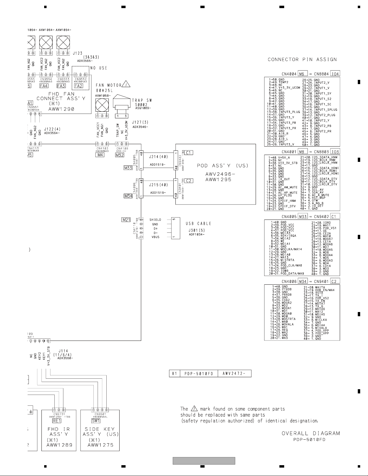
4. BLOCK DIAGRAM .............................................................................................................................................................. 20
4.1 OVERALL WIRING DIAGRAM (1/2)............................................................................................................................. 20
4.2 OVERALL WIRING DIAGRAM (2/2)............................................................................................................................. 22
4.3 OVERALL BLOCK DIAGRAM (1/2).............................................................................................................................. 24
4.4 OVERALL BLOCK DIAGRAM (2/2).............................................................................................................................. 26
4.5 POWER SUPPLY UNIT ................................................................................................................................................ 28
4.6 50F X DRIVE ASSY...................................................................................................................................................... 29
4.7 50F Y DRIVE, 50F SCAN A, B, C and D ASSYS ......................................................................................................... 30
4.8 POWER SUPPLY BLOCK of 50F X, Y DRIVE and 50F SCAN A, B, C and D ASSYS ................................................ 31
4.9 50F ADDRESS L and S ASSYS................................................................................................................................... 32
4.10 50F DIGITAL ASSY .................................................................................................................................................... 33
4.11 MAIN ASSY (DTV BLOCK DIAGRAM)....................................................................................................................... 34
4.12 POWER SUPPLY BLOCK of MAIN ASSY.................................................................................................................. 36
4.13 TANSHI ASSY ............................................................................................................................................................ 38
4.14 50FHD LED and FHD IR ASSYS ............................................................................................................................... 39
4.15 POWER SUPPLY BLOCK of FHD RLS and SIDE KEY ASSYS ................................................................................ 40
5. DIAGNOSIS ........................................................................................................................................................................ 41
5.1 POWER SUPPLY OPERATION.................................................................................................................................... 41
5.1.1 LED DISPLAY INFORMATION............................................................................................................................... 41
5.1.2 POWER ON SEQUENCE ...................................................................................................................................... 42
5.1.3 DETAILS OF POWER ON SEQUENCE................................................................................................................. 43
5.2 DIAGNOSIS FLOWCHART OF FAILURE ANALYSIS .................................................................................................. 45
5.2.1 WHOLE UNIT......................................................................................................................................................... 45
5.2.2 POWER SUPPLY UNIT.......................................................................................................................................... 47
5.2.3 DRIVE ASSY.......................................................................................................................................................... 48
5.2.4 DIGITAL ASSY ....................................................................................................................................................... 52
5.2.5 MAIN ASSY............................................................................................................................................................ 53
5.2.6 VIDEO SYSTEM .................................................................................................................................................... 54
5.2.7 AUDIO SYSTEM ....................................................................................................................................................60
5.3 DIAGNOSIS OF PD (POWER-DOWN) ........................................................................................................................ 63
5.3.1 BLOCK DIAGRAM OF THE POWER-DOWN SIGNAL .......................................................................................... 63
5.3.2 PD (POWER-DOWN) DIAGNOSIS OF FAILURE ANALYSIS ................................................................................ 64
5.4 DIAGNOSIS OF SD (SHUTDOWN) ............................................................................................................................. 67
5.4.1 BLOCK DIAGRAM OF THE SHUTDOWN SIGNAL............................................................................................... 67
5.4.2 SD (SHUTDOWN) DIAGNOSIS............................................................................................................................. 68
5.5 NON-FAILURE INFORMATION .................................................................................................................................... 70
5.5.1 INFORMATION ON SYMPTOMS THAT DO NOT CONSTITUTE FAILURE.......................................................... 70
5.5.2 FUNCTION OF DECREASING THE BRIGHTNESS LEVEL................................................................................. 73
5.6 OUTLINE OF THE OPERATION .................................................................................................................................. 74
5.6.1 PANEL DRIVE-POWER ON / OFF FUNCTION ..................................................................................................... 74
5.6.2 SPECIFICATION OF THE FAN CONTROL............................................................................................................75
5.6.3 PROCESSING IN ABNORMALITY........................................................................................................................ 76
5.6.4 TRAP SWITCH.......................................................................................................................................................79
A
B
C
D
E
PDP-5010FD
56
F
5
7
8
Page 6

1234
6. SERVICE FACTORY MODE................................................................................................................................................80
6.1 OUTLINE OF THE SERVICE FACTORY MODE ..........................................................................................................80
A
6.1.1 SERVICE FACTORY MODE TRANSITION CHART...............................................................................................80
6.1.2 HOW TO ENTER/EXIT SERVICE FACTORY MODE .............................................................................................80
6.1.3 FUNCTIONS WHEN ENTERING THE SERVICE FACTORY MODE .....................................................................81
6.1.4 REMOTE CONTROL CODE IN SERVICE FACTORY MODE ................................................................................82
6.1.5 PDP SERVICE REMOTE CONTROL.....................................................................................................................83
6.1.6 FACTORY HIERARCHICAL TABLE .......................................................................................................................84
6.1.7 INDICATIONS IN SERVICE FACTORY MODE ......................................................................................................86
6.2 DETAILS OF FACTORY MENU ....................................................................................................................................88
6.2.1 INFORMATION .......................................................................................................................................................88
6.2.2 PANEL FACTORY (+) .............................................................................................................................................98
6.2.3 OPTION................................................................................................................................................................108
6.2.4 INITIALIZE............................................................................................................................................................109
B
7. DISASSEMBLY..................................................................................................................................................................112
7.1 FLOWCHART OF REMOVAL ORDER FOR THE MAIN PARTS AND BOARDS .......................................................112
7.2 DISASSEMBLY ...........................................................................................................................................................113
7.3 DISASSEMBLY AND REASSEMBLY PRECAUTIONS FOR SPEAKER SYSTEM.....................................................121
8. EACH SETTING AND ADJUSTMENT ..............................................................................................................................122
8.1 ADJUSTMENT REQUIRED WHEN THE UNIT IS REPAIRED OR REPLACED ........................................................122
8.2 BACKUP OF THE EEPROM (DIGITAL ASSY) ...........................................................................................................124
8.3 HOW TO CLEAR HISTORY DATA ..............................................................................................................................127
8.4 ADJUSTMENT WHEN THE SERVICE PANEL ASSY IS REPLACED .......................................................................128
8.5 ADJUSTMENT WHEN THE DRIVE ASSYS ARE REPLACED ..................................................................................141
8.6 PRECAUTION ON REPLACEMENT OF THE POWER SUPPLY UNIT......................................................................144
9. RS-232C............................................................................................................................................................................145
C
9.1 OUTLINE OF RS-232C COMMAND...........................................................................................................................145
9.1.1 PREPARED TOOLS .............................................................................................................................................145
9.1.2 USING RS-232C COMMANDS............................................................................................................................145
9.2 LIST OF RS-232C COMMANDS ................................................................................................................................146
9.3 DETAILS OF EACH COMMANDS ..............................................................................................................................155
9.3.1 QS1 (PANEL STATUS) .........................................................................................................................................155
9.3.2 QS2 (PANEL OPERATION DATA) ........................................................................................................................156
9.3.3 QS3 (OTHER DATA ON THE PANEL) ..................................................................................................................157
9.3.4 QAJ (PANEL ADJUSTMENT DATA) .....................................................................................................................158
9.3.5 QPW (VIDEO ADJUSTMENT DATA OF THE PANEL) .........................................................................................159
9.3.6 QPM (PULSE METER VALUE) ............................................................................................................................159
D
9.3.7 QPD (PD LOGS) ..................................................................................................................................................160
9.3.8 QSD (SD LOGS) ..................................................................................................................................................161
9.3.9 QSE (DESTINATION PECULIAR INFORMATION) ..............................................................................................162
9.3.10 QMT (TEMPERATURE / FAN ROTATION / ROOM LIGHT SENSOR) ...............................................................162
9.3.11 QNG (SHUTDOWN INFORMATION OF MTB)...................................................................................................163
9.3.12 QSI (INPUT SIGNAL DATA)................................................................................................................................165
9.3.13 DRV (PANEL DRIVE-POWER ON / OFF) ..........................................................................................................165
9.3.14 FAY / FAN (ADJ. COMMANDS PERMISSION / PROHIBITION) ........................................................................166
9.3.15 FAJ / UAJ / CBU / BCP (BACKUP FUNCTION FOR ADJUSTMENT VALUE) ...................................................166
10. EXPLODED VIEWS AND PARTS LIST...........................................................................................................................168
10.1 PACKING SECTION .................................................................................................................................................168
10.2 REAR SECTION .......................................................................................................................................................170
E
10.3 FRONT SECTION.....................................................................................................................................................172
10.4 CHASSIS SECTION (1/2).........................................................................................................................................174
10.5 CHASSIS SECTION (2/2).........................................................................................................................................176
10.6 PANEL CHASSIS SECTION .....................................................................................................................................178
10.7 MULTI BASE SECTION ............................................................................................................................................180
10.8 PDP SERVICE ASSY 508F (AWU1272)...................................................................................................................182
10.9 TABLE TOP STAND ..................................................................................................................................................184
10.10 SPEAKER SYSTEM (PACKING) ............................................................................................................................185
10.11 CS ASSY ................................................................................................................................................................186
F
6
1 234
PDP-5010FD
Page 7

5678
1. SERVICE PRECAUTIONS
1.1 NOTES ON SOLDERING
• For environmental protection, lead-free solder is used on the printed circuit boards mounted in this unit.
Be sure to use lead-free solder and a soldering iron that can meet specifications for use with lead-free solders for repairs
accompanied by reworking of soldering.
• Compared with conventional eutectic solders, lead-free solders have higher melting points, by approximately 40 °C.
Therefore, for lead-free soldering, the tip temperature of a soldering iron must be set to around 373 °C in general, although
the temperature depends on the heat capacity of the PC board on which reworking is required and the weight of the tip of
the soldering iron.
A
Compared with eutectic solders, lead-free solders have higher bond strengths but slower wetting times and higher melting
temperatures (hard to melt/easy to harden).
The following lead-free solders are available as service parts:
• Parts numbers of lead-free solder:
GYP1006 1.0 in dia.
GYP1007 0.6 in dia.
GYP1008 0.3 in dia.
B
C
D
PDP-5010FD
56
E
F
7
7
8
Page 8
1234
1.2 CHARGED SECTION AND HIGH VOLTAGE GENERATING POINT
A
Charged Section
The places where the commercial AC power is used without
passing through the power supply transformer.
If the places are touched, there is a risk of electric shock. In
addition, the measuring equipment can be damaged if it is
connected to the GND of the charged section and the GND of the
non-charged section while connecting the set directly to the
commercial AC power supply. Therefore, be sure to connect the
set via an insulated transformer and supply the current.
1. Power Cord
B
2. AC Inlet
3. Power Switch
4. Fuse (In the POWER SUPPLY Unit)
5. STB Transformer and Converter Transformer
(In the POWER SUPPLY Unit)
6. Other primary side of the POWER SUPPLY Unit
C
: Part is Charged Section.
: Part is the High Voltage Generating Points
other than the Charged Section.
High Voltage Generating Point
The places where voltage is 100 V or more except for the charged
places described above. If the places are touched, there is a risk of
electric shock.
The VSUS voltage remains for several minutes after the power to
the unit is turned off. These places must not be touched until
about 10 minutes after the power is turned off, or it is confirmed
with a tester that there is no residual VSUS voltage.
If the procedures described in “5.6.1 PANEL DRIVE-POWER
ON/OFF FUNCTION” are performed before the power is turned
off, the voltage will be discharged in about 30 seconds.
POWER SUPPLY UNIT ................................................... (205 V)
50F X DRIVE Assy .......................................................... (205 V)
50F Y DRIVE Assy ......................................... (−270 V to 400 V)
50F SCAN A Assy .......................................... (−270 V to 400 V)
50F SCAN B Assy ........................................... (−270 V to 400 V)
50F SCAN C Assy ........................................... (−270 V to 400 V)
50F SCAN D Assy ........................................... (−270 V to 400 V)
50F Y DRIVE Assy POWER SUPPLY Unit 50F X DRIVE Assy Conductive plate X
D
Assy
50F SCAN A
Assy
50F SCAN B
E
Assy
50F SCAN C
Assy
50F SCAN D
F
AC inlet Power switch
Fig. High Voltage Generating Point (Rear view)
8
1 234
PDP-5010FD
Page 9
5678
2. SPECIFICATIONS
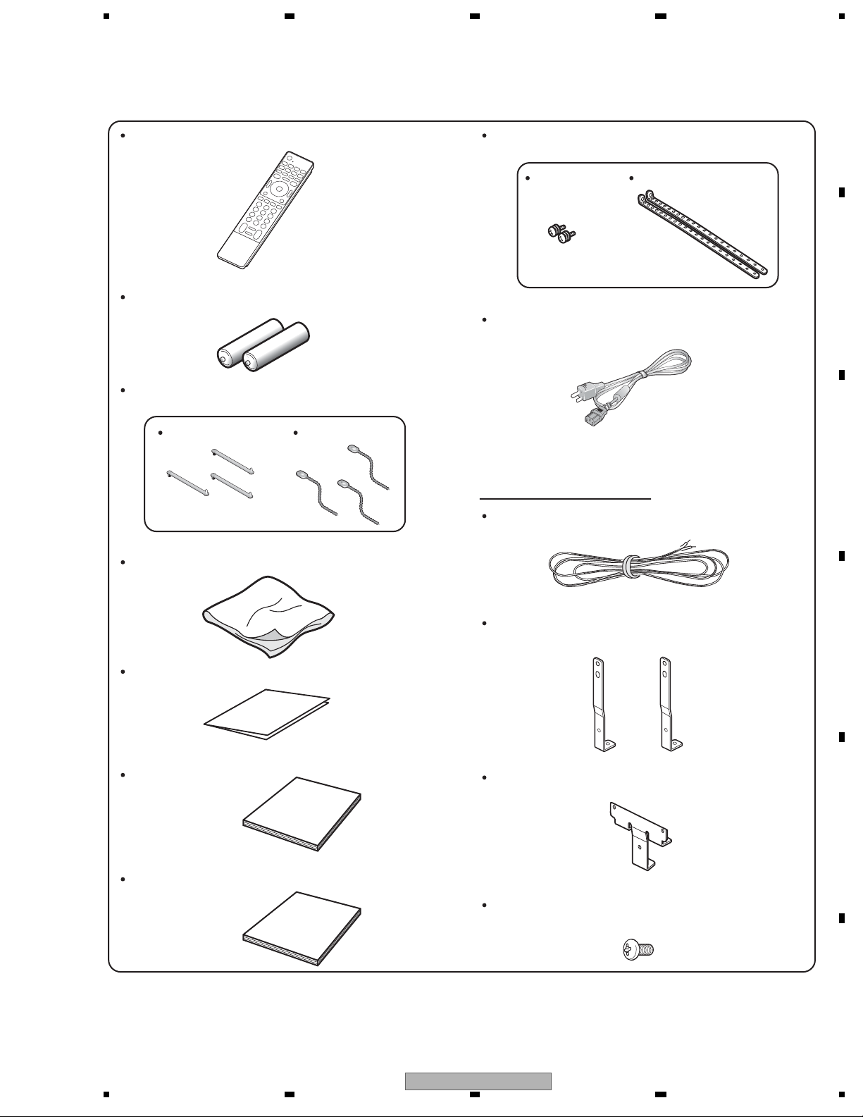
2.1 ACCESSORIES
A
Remote control unit
(AXD1550)
Alkaline dry cell battery (LR6, AA)
Binder Assy
(AEC1908)
Speed clamp: ×3
Bead band: ×3
Band assy
(AXY1192)
Screw: ×2
(M4×10 mm)
(for plastic bands)
Power cord (2 m/6.6 feet)
(ADG1215)
Plastic band: ×2
Speaker accessories
Speaker cable: ×2
(SDS1202)
B
C
Cleaning cloth (AED1285)
Warranty card
Operating instructions
(PDP-5010FD/KUCXC)
(ARE1472)
Operating instructions
(PDP-5010FD/KUC)
(ARE1487)
Bracket Assy (S): ×2
(SXG1127)
Brackets for side: ×2
Bracket Assy (C)
(SXG1128)
Brackets for center
Speaker mounting screw (M5 x 10 mm: Black): ×9
(BMZ50P100FTB)
D
E
PDP-5010FD
56
F
9
7
8
Page 10
1234
2.2 SPECIFICATIONS
A
Item
Number of pixel
Audio Amplifier
Speakers
Sound Effect
Power Requirement
Weight
B
Reception System (Digital)
Circuit type
Tuner
Audio format Dolby Digital
Reception System (Analog)
Circuit type
Tuner
Audio multiplex
Terminals Rear 75 Ω UNBAL, F Type for DTV/VHF/UHF/CATV in
C
D
Side INPUT 3
On-screen display languages
VHF/UHF
CATV
VHF/UHF
CATV
ANT/CABLE A IN
ANT B IN
INPUT 1
INPUT 2
INPUT 4
PC INPUT
INPUT 5
INPUT 6
INPUT 7
AUDIO OUT AUDIO out (Fixed)
DIGITAL OUT
CONTROL OUT 1
SPEAKERS
SUB WOOFER Variable
CableCARD
PHONES 16 Ω to 32 Ω recommended
USB USB in**
* This conforms to HDMI1.3 and HDCP1.1.
HDMI (High Definition Multimedia Interface) is a digital interface that handles both video and audio using a single cable.
HDCP (High-bandwidth Digital Content Protection) is a technology used to protect copyrighted digital contents that use
the Digital Visual Interface (DVI).
** This conforms to USB 1.1 and 2.0 .
E
• Design and specifications are subject to change without notice.
1920 × 1080 pixels
17 W + 17 W (1 kHz, 10 %, 6 Ω)
Woofer: 4.8 cm x 13 cm cone type
Tweeter: 2.5 cm semidome type
SRS FOCUS/SRS/SRS TruBass
120 V AC, 60 Hz, 442 W (26 W Standby)
Main unit: 38.5 kg (84.9 lbs.)
Stand: 2.2 kg (4.9 lbs.) (including bolts)
Speaker system: 3.3 kg (7.3 lbs.) (including
cables, mounting fittings and screws)
Total: 44.0 kg (97 lbs.)
ATSC Digital TV system
8VSB/64QAM/256QAM/QPSK demodulation
VHF Ch. 2 to 13 UHF Ch. 14 to 69
Ch. 2 to 135
American TV standard NTSC system
Video signal detection PLL full synchronous detection, PLL digital Synthesizer system
VHF Ch. 2 to 13 UHF Ch. 14 to 69
ANT/CABLE A IN Ch. 1 to 135 ANT B IN Ch. 1 to 125
BTSC system
75 Ω UNBAL, F Type for VHF/UHF/CATV in
S-VIDEO in, VIDEO in, AUDIO in
COMPONENT VIDEO in, VIDEO in, AUDIO in
HDMI in*, AUDIO in
Analog RGB in, AUDIO in
HDMI in*, AUDIO in
HDMI in*
HDMI in*
Optical
6 Ω to 16 Ω
Point of Deployment
COMPONENT VIDEO in, VIDEO in, AUDIO in
English/French/Spanish
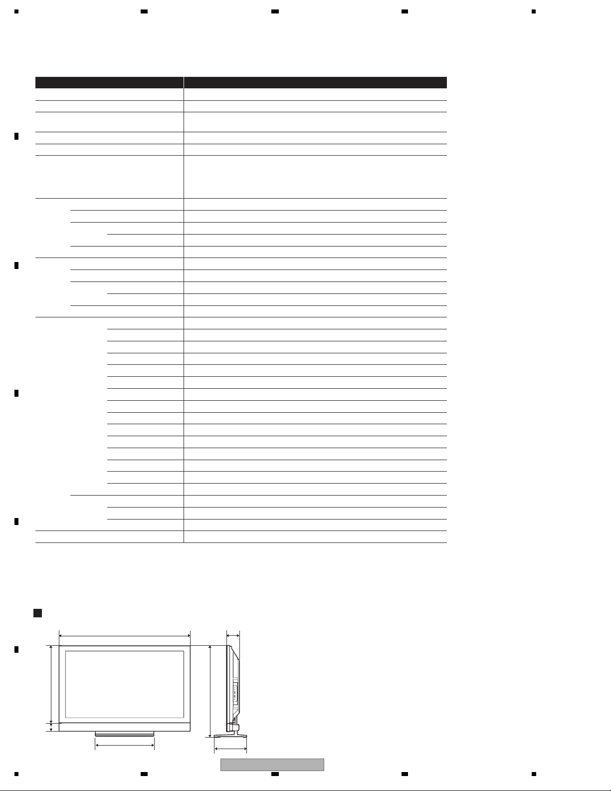
Dimensions
1232 (48-1/2)
722 (28-7/16)
F
80 (3-5/32)
550 (21-21/32)
10
1 234
120 (4-23/32)
850 (33-15/32)
300 (11-13/16)
Unit: mm (inch)
PDP-5010FD
Page 11
5678
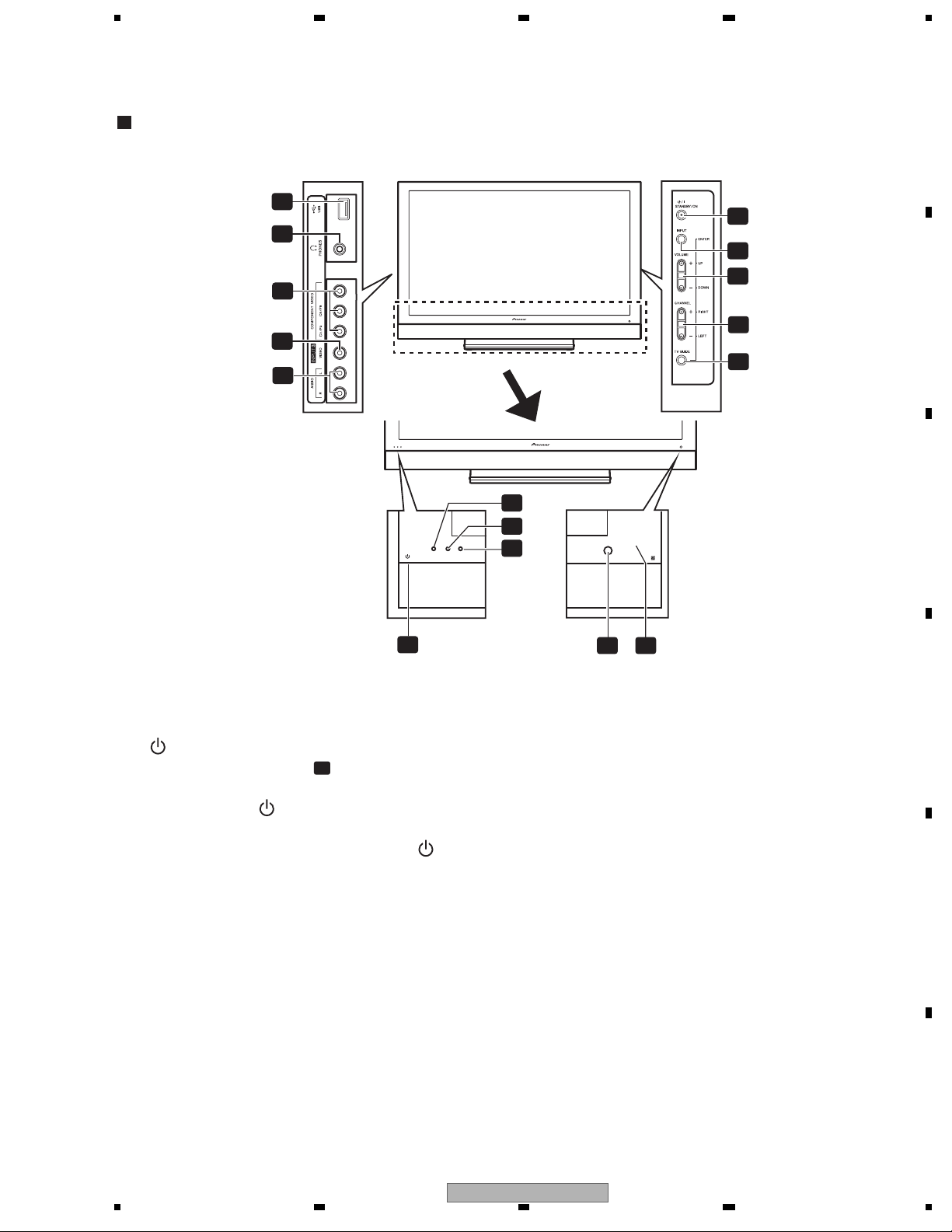
2.3 PANEL FACILITIES
Front Section
12
13
14
15
16
Side
ON STANDBY SLEEP
A
Side
7
8
9
B
10
11
2
C
3
4
1
1
button (This button is located on the bottom
on the rear panel (see on Rear section).
If the button is off, the power will not turn on
even when
STANDBY/ON
TV
on the remote control unit or
on the plasma display is
pressed. To turn on the power, press ).
2
POWER ON indicator
3
STANDBY indicator
4
SLEEP indicator
5
Room Light Sensor
6
Remote control sensor
7 STANDBY/ON
button
1
1
5
6
8 INPUT
9 VOLUME UP/DOWN
button (
ENTER
button*)
buttons (
UP/DOWN
buttons*)
10 CHANNEL UP/DOWN
buttons (
LEFT/RIGHT
buttons*)
11 TV GUIDE
12
USB port
13
PHONES output terminal
14
INPUT 3 terminals (COMPONENT VIDEO: Y, PB,
P
R
)
15
INPUT 3 terminal (VIDEO)
16
INPUT 3 terminals (AUDIO)
The buttons with asterisks (*) can operate the TV Guide On
Screen™ system.
button*
D
E
PDP-5010FD
56
F
11
7
8
Page 12
A
Rear Section
B
1234
45
21
19
20
13
45
45
14
15
1
C
17
16
22
23
26
2 3
27
4
18
25 24
6
7 85
D
1
button
2
CableCARD™ slot
3
ANT/CABLE A IN terminal
4
E
F
AC IN terminal
5
INPUT 4 terminal (HDMI)
6
INPUT 5 terminal (HDMI)
7
INPUT 6 terminal (HDMI)
8
INPUT 7 terminal (HDMI)
9
PC INPUT terminal (ANALOG RGB)
10
CONTROL OUT terminal
11
RS-232C terminal (used for factory setup)
12
ANT B IN terminal
13
INPUT 1 terminal (S-VIDEO)
14
INPUT 1 terminal (VIDEO)
15
SUB WOOFER terminal
16
AUDIO OUT terminals (AUDIO)
* For exact terminal positions, refer to
the terminal position sheet located
near the terminal compartment.
17
INPUT 1 terminals (AUDIO)
18
INPUT 2 terminals (AUDIO)
19
INPUT 4 terminals (AUDIO)
20
INPUT 5 terminals (AUDIO)
21
INPUT 2 terminal (VIDEO)
22
DIGITAL OUT terminal (OPTICAL)
23
PC INPUT terminal (AUDIO)
24
INPUT 2 terminals (COMPONENT VIDEO: Y, PB,
PP
25
26
27
R
)
SPEAKERS (R/L) terminals
SPEAKERS (R) terminal (Speaker side)
SPEAKERS (L) terminal (Speaker side)
9
10
11
12
12
PDP-5010FD
1 234
Page 13
5678
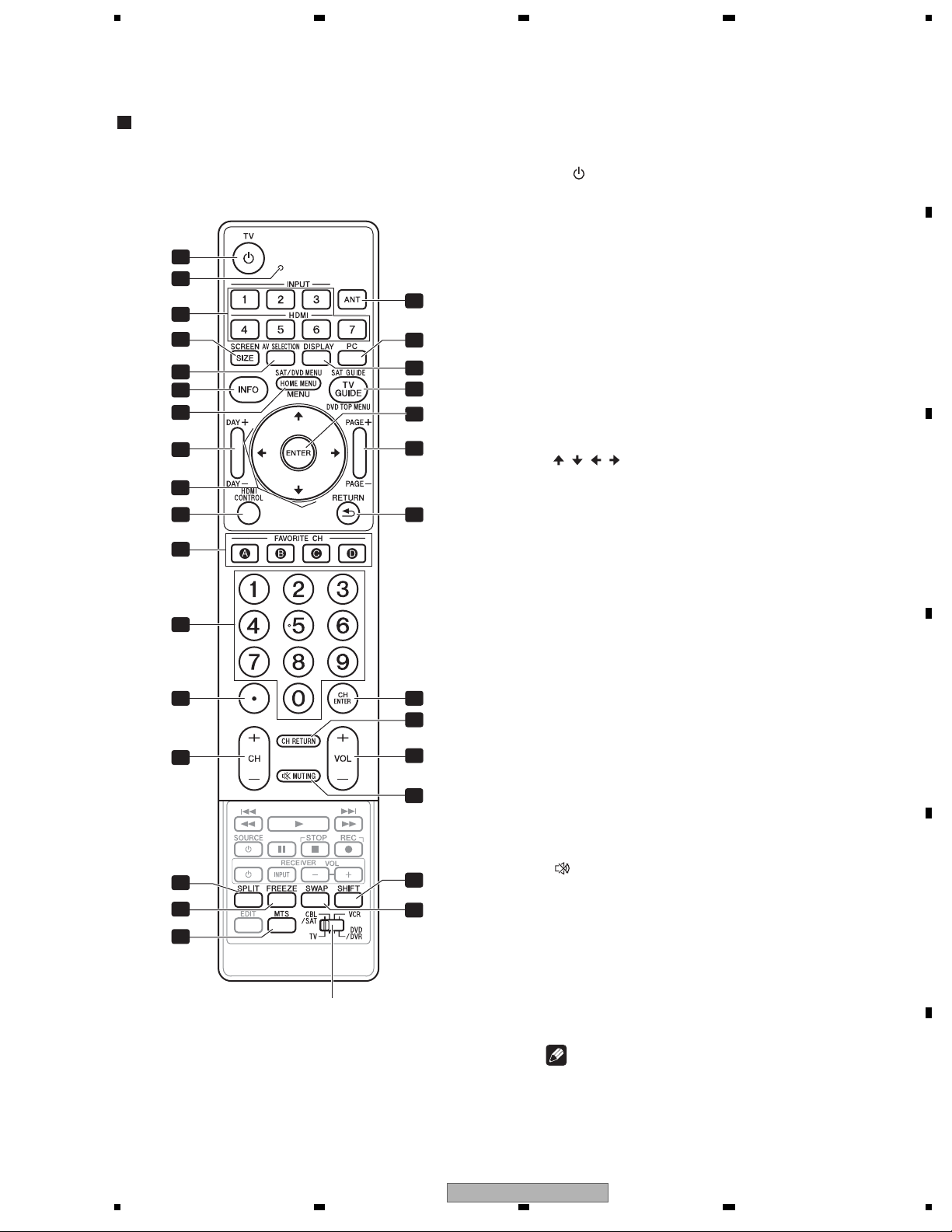
Remote Control Unit
This section describes the functions of the buttons available
when the mode switch has been set to TV.
1
2
3
4
5
6
7
8
9
10
11
12
13
14
15
16
17
Mode switch
(with “TV” selected)
18
19
20
21
22
23
24
25
26
27
28
29
30
1 TV
:
into standby mode.
2
3 INPUT
(“INPUT1”, “INPUT 2 ”, “INPUT3”, “INPUT4”, “INPUT5”,
“INPUT6” and “INPUT 7 ”)
4 SCREEN SIZE
5 AV SELECTION
OPTIMUM, STANDARD, DYNAMIC, MOVIE, GAME, USER.
PC source: STANDARD, USER.)
6 INFO
watched.
When the TV Guide On Screen™ system is in operation, displays
information about the currently highlighted channel (if available).
7 HOME MENU
MENU
system is in operation.
8 DAY +/–
in the TV Guide On Screen™ Listing service.
9
10 HDMI CONTROL
11 FAVORITE CH (A, B, C, D)
Selects any of the four preset channels.
While watching, you can toggle the set channels by pressing
B, C
12 0 to 9
13 • (dot)
14 CH +/–
15 SPLIT
picture, and single-screen.
16 FREEZE
cancel the function.
17 MTS
being watched.
18 ANT
19 PC
20 DISPLAY
21 TV GUIDE
22 ENTER
23 PAGE +/–
program listing screen vertically.
24 RETURN
25 CH ENTER
26 CH RETURN
disabled while the TV Guide On Screen™ system is displayed.
27 VOL +/–
28
29 SHIFT
picture-in-picture mode.
30 SWAP
or picture-in-picture mode.
Luminous remote control buttons
All buttons on the remote control unit are luminous and gather
and store light. This enables quick access to the desired
function when performing operations in dark places.
Turns on the power to the plasma display or places it
Transmission confirmation LED
: Selects an input source of the plasma display.
: Selects the screen size.
: Selects audio and video settings.
: Displays a channel banner when a TV program is being
: Displays the HOME MENU screen.
: Displays a panel menu when the TV Guide On Screen™
: Jumps to the next or previous day of program listings
/ / / : Selects a desired item on the menu screen.
and D.
: Selects the channel.
: Enters a dot.
: Selects the channel.
: Switches the screen mode among 2-screen, picture-in-
: Freezes a frame from a moving image. Press again to
: Selects MTS/SAP or language depending on the program
: Selects the antenna (A, B).
: Selects the PC terminal as an input source.
: Executes a command.
: Sets the volume.
MUTING
: Moves the location of the small screen when in the
: Switches between the two screens when in the 2-screen
: Displays the HDMI Control menu.
:
: Displays the channel information.
: Displays the TV Guide On Screen™ system.
(for the TV Guide On Screen™ system): Scrolls the
: Returns to the previous menu screen.
: Executes a channel number.
: Returns to the previous channel. This button is
: Mutes the sound.
(AV source:
A
,
A
B
C
D
E
Note
• When using the remote control unit, point it at the plasma
display.
PDP-5010FD
56
F
13
7
8
Page 14
1234
3. BASIC ITEMS FOR SERVICE
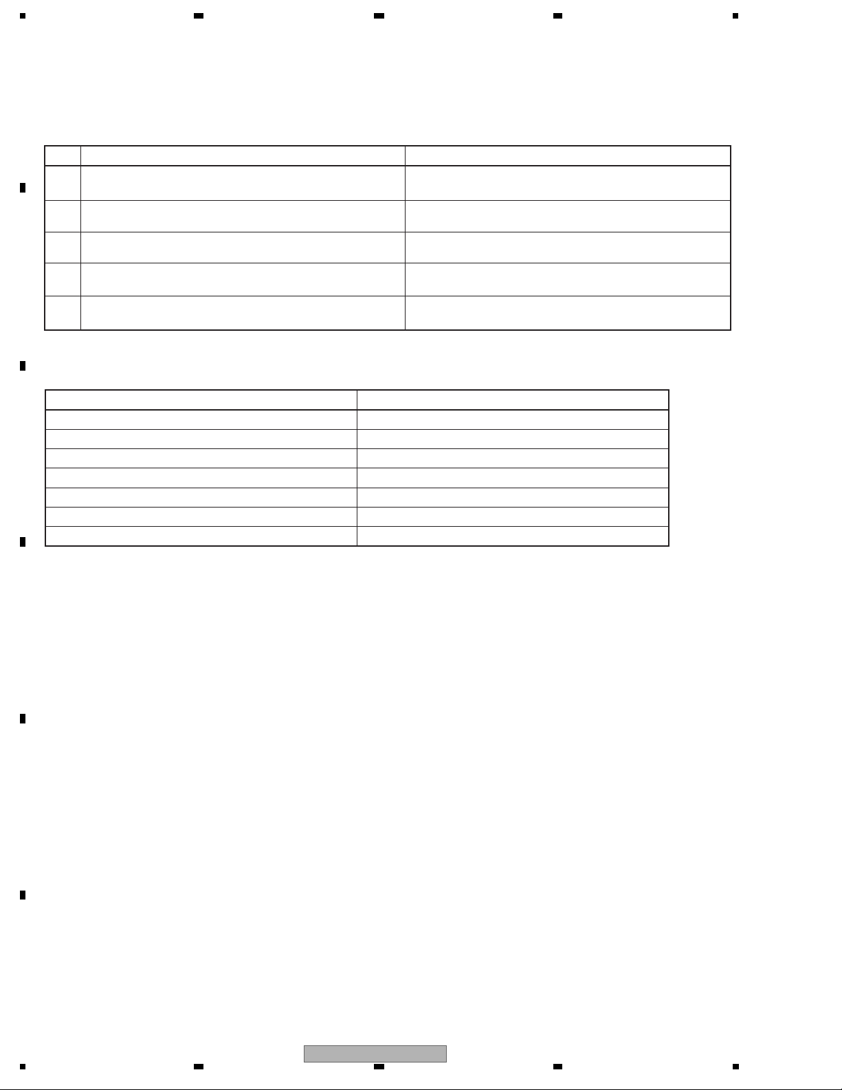
3.1 CHECK POINTS AFTER SERVICING
A
Items to be checked after repair (PDP)
To ensure the quality of the product after repair, check the recommended items shown below:
No. Procedures Item to be checked
Check if all the symptoms pointed out by the customer have been
1
addressed.
2 Connect the peripheral equipment.
3 Check the video and audio.
B
4 Check the buttons and controls.
5 Check the cabinet.
See the table below for the items to be checked regarding video and audio:
Item to be checked regarding video Item to be checked regarding audio
Block noise Distortion
Horizontal noise Noise
C
Dot noise Volume too low
Disturbed image (video jumpiness) Volume too high
Too dark Volume fluctuating
Too bright Sound interrupted
Mottled color
The symptoms in question must not be reproduced.
Connect all external peripheral equipment as originally connected
and check if the connections are correct.
Tune in to the stations that the customer would normally receive
and check if video and audio are normal.
Use the buttons and controls on the remote control unit and main
unit and check if they operate properly.
Check for any scratches or dirt that have been made or attached
on the cabinet after receiving the product for repair.
D
E
F
14
PDP-5010FD
1 234
Page 15
5678
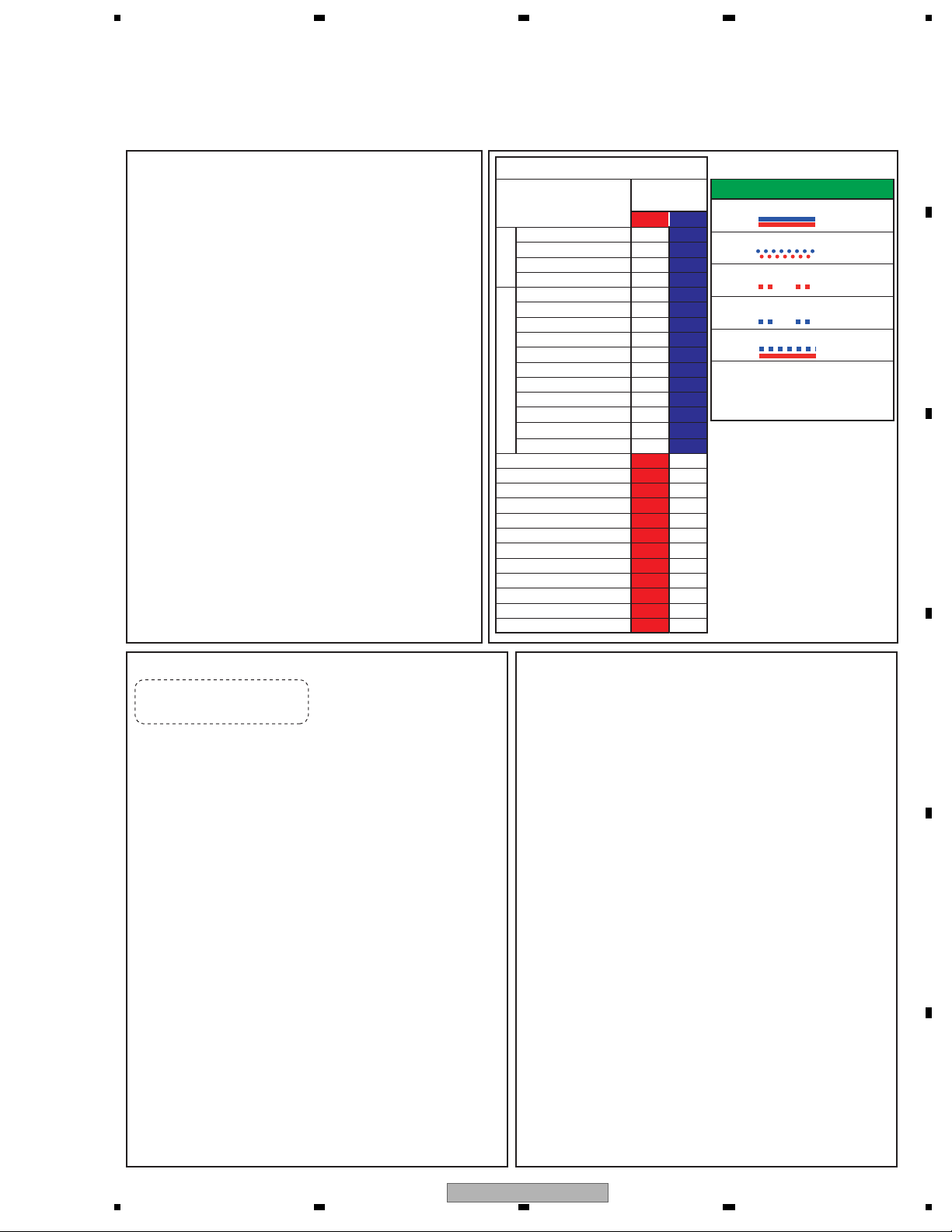
3.2 QUICK REFERENCE
Quick Reference upon Service Visit 1
Notes, PD/SD diagnosis, and methods for various settings
Notes when visiting for service
1. Notes when disassembling/reassembling
1 Rear case
When reassembling the rear case, the screws must be tightened in a
specific order. Be careful not to tighten them in the wrong order forcibly.
For details, see "Rear Case" in "7. DISASSEMBLY".
2 Attaching screws for the HDMI connector
When attaching the HDMI connector after replacing the Main Assy,
secure the HDMI connector manually with a screwdriver, but not
with an electric screwdriver. If you tighten the screws too tightly
with an electric screwdriver, the screw heads may be damaged, in
which case the screws cannot be untightened/tightened any more.
2. On parts replacement
1 How to discharge before replacing the Assys
A charge of significant voltage remains in the Plasma Panel even
after the power is turned off. Safely discharge the panel before
replacement of parts, in either manner indicated below:
Let the panel sit at least for 3 minutes after the power is turned off.
A:
B: Turn the Large Signal System off before the power is turned off
then, after 1 minute, turn the power off.
For details, see "5.6.1 PANEL DRIVE-POWER ON/OFF
FUNCTION".
2 On the settings after replacement of the Assys
Some boards need settings made after replacement of the Assys.
For details, see "8. EACH SETTING AND ADJUSTMENT".
3. On various settings
1 Setting in Factory mode
After a Mask indication into the panel is performed, be sure to
set the Mask setting to "OFF" then exit Factory mode.
PD/SD
Item
SQ_LSI
Communication with the module IIC
DIGITAL-RST2
Panel high temperature
Panel section
Audio/
Short-circuit SP terminal
Communication with the Module UCOM
Main 3-wire serial communication
Main IIC communication
Communication with the Main UCOM
FAN
Unit high temperature
MTB section
Digital Tuner communication
MTB-RST2/RST4
Home Media Gallery
Main EEPROM
POWER
SCAN
SCN-5V
Y-DRIVE
Y-DCDC
Y- S U S
ADRS
X-DRIVE
X-DCDC
X-SUS
DIG-DCDC
UNKNOWN
No. of LEDs
flashing
Red Blue
Blue 1
Blue 2
Blue 3
Blue 4
Blue 5
Blue 6
Blue 7
Blue 8
Blue 9
Blue 10
Blue 11
Blue 12
Blue 13
Blue 14
Blue 15
Red 2
Red 3
Red 4
Red 5
Red 6
Red 7
Red 8
Red 9
Red 10
Red 11
Red 12
Red 15
LED Display Information
1 TRAP SW
2 Rewriting software
3 PD (2-15)
4 SD (1-15)
5 No backup
This indication does not display all
LED patterns.
For details, please refer to 5.1.1 LED
DISPLAY INFORMATION.
A
B
C
How to locate several items on the Factory menu
{ } : Item on the Factory menu
[ ] : Key on the remote control unit
" " : Screen indication
1. Confirmation of accumulated power-on time and power-on
count
Select {INFORMATION} then {HOUR METER}.
(After entering Factory mode, press [j] five times.)
2. Confirmation of the Power-down and Shutdown histories
1 Panel system
PD: Select {PANEL FACTORY} then {POWER DOWN}.
(After entering Factory mode, press [MUTING] once, press
[ENTER/SET], then press [j] three times.)
SD: Select {PANEL FACTORY} then {SHUT DOWN}.
(After entering Factory mode, press [MUTING] once, press
[ENTER/SET], then press [j] four times.)
2 MTB section
Select {INFORMATION} then {MAIN NG}.
(After entering Factory mode, press [j] three times.)
3. How to display the Mask indication
1 Mask indication in the panel side
1. Select {PANEL FACTORY} then {RASTER MASK SETUP}.
(After entering Factory mode, press [MUTING] once, press
[ENTER/SET], then press [j] 8 times.)
2. Press [ENTER/SET], then select a Mask indication, using [i] or [j].
Adjustments and Settings after replacement of the
Assys (Procedures in Factory mode)
1. Digital Video Assy: Transfer of backup data
1 Select {PANEL FACTORY}, {ETC}, then {BACKUP DATA}. (After entering Factory
mode, press [MUTING] once, press [ENTER/SET], press [j] seven times, then
press [ENTER/SET].)
2 Select {TRANSFER}, using [l], then hold [ENTER/SET] pressed for at least 5
seconds.
3 After transfer of backup data is completed, {ETC} is automatically selected, and the
LED on the front panel returns to normal lighting.
2. MAIN Assy: Execution of FINAL SETUP.
1 Select {INITIALIZE} then {FINAL SETUP}, then press [ENTER/SET]. (After entering
Factory mode, press [MUTING] three times, then press [j] four times.)
2 Select "YES", using [l]. Then hold [ENTER/SET] pressed for at least 5 seconds.
3 After "FINAL SETUP IS COMPLETE" is displayed on the screen, turn the POWER
switch of the main unit off.
3. POWER SUPPLY Unit: Clearance of the accumulated power-on count
and maximum temperature value
1 Select {PANEL FACTORY}, {ETC}, then {P COUNT INFO}. (After entering Factory
mode, press [MUTING] once, press [ENTER/SET], press [j] seven times, press
[ENTER/SET], then press [j] six times.)
2 Press [l] to select "CLEAR". Hold [ENTER/SET] pressed for at least 5 seconds.
After clearance is completed, "ETC" is automatically selected. Clear the maximum
temperature value (MAX TEMP) in the same manner.
4. Other Assys: Clearance of the maximum temperature value
1 Select {PANEL FACTORY}, {ETC}, then {MAX TEMP}. (After entering Factory mode,
press [MUTING] once, press [ENTER], press [j] seven times, press [ENTER/SET],
then press [j] seven times.)
2 Press [l] to select "CLEAR". Hold [ENTER/SET] pressed for at least 5 seconds.
After clearance is completed, "ETC" is automatically selected.
D
E
F
PDP-5010FD
56
15
7
8
Page 16
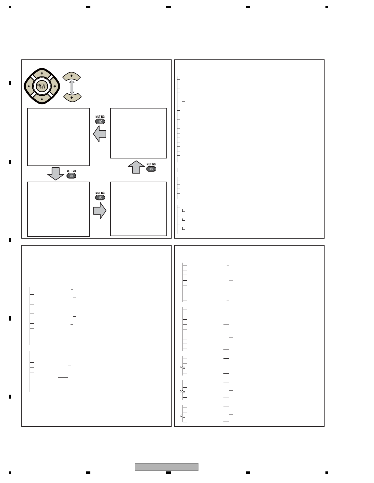
1234
A
Mode transition in Service Factory mode
INFORMATION mode
1. VERSION (1)
B
C
2. VERSION (2), (3)
3. MAIN NG
4. TEMPERATURE
5. HOUR METER
6. HDMI SIGNAL INFO 1
7. HDMI SIGNAL INFO 2
8. VDEC SIGNAL INFO 1
9. VDEC SIGNAL INFO 2
10. DTV TUNING STATUS 1, 2, 3
11. DTV TV-GUIDE BER
12. DEBUG INFO
PANEL FACTORY mode
1. PANEL INFORMATION
2. PANEL WORKS
3. POWER DOWN
4. SHUT DOWN
5. PANEL-1 ADJ
6. PANEL-2 ADJ
7. PANEL FUNCTION
8. ETC.
9. RASTER MASK SETUP
10. PATTEN MASK SETUP
11. COMBI MASK SETUP
Mode transition and structure of layers in Service Factory mode
Up
Down
Quick Reference upon Service Visit 2
• To shift to another mode, press [MUTING].
• To shift to another item in a specific mode,
press [i] or [j].
• To shift to the next nested layer below for an
item with a "(+)" indication, press [ENTER/SET].
To return to the next nested layer above,
also press [ENTER/SET].
INITIALIZE mode
1. SIDE MASK LEVEL
2. FINAL SETUP
3. Wide XGA AUTO
OPTION mode
1. EDID WRITE MODE
2. ANTENNA MODE
3. AFT
4. SYNC DET
Structure of Layers in Service Factory Mode
INFORMATION mode
1. VERSION (1) The software versions for each microcomputer
2. VERSION (2) The Flash memory versions for each device
3. VERSION (3) The Flash memory versions for each device
4. MAIN NG The shutdown message ID/event times
(Going Clear mode by [ENTER/SET] key)
4-1. CLEAR
5. TEMPERATURE The temperature/FAN rotating status/Room Light Sensor
6. HOUR METER The HOUR METER/P-COUNT information
6-1. CLEAR
7. HDMI SIGNAL INFO 1 The information of HDMI information files
8. HDMI SIGNAL INFO 2 The information of HDMI information files
9. VDEC SIGNAL INFO 1 The signal information of VDEC
10. VDEC SIGNAL INFO 2 The signal information of VDEC
11. DTV TUNING STATUS 1 Detail information for DTV
12. DTV TUNING STATUS 2 Detail information for DTV
13. DTV TUNING STATUS 3 Detail information for DTV
14. DTV TV-GUIDE BER For production line use
15. DEBUG INFO For factory use
PANEL FACTORY mode Refer to [PANEL FACTORY MODE]
OPTION mode
1. EDID WRITE MODE For factory use
2. ANTENNA MODE For production line use
3. AFT For production line use
4. SYNC DET For technical analysis
INITIALIZE mode
1. SIDE MASK LEVEL For factory use
1-1. SIDE MASK LEVEL
2. FINAL SETUP Set to Factory default settings (it should perform after
2-1. DATA RESET replacing a MAIN Assy)
3. HMG/HG SERVICE MODE Information for a USB device is displayed
3-1. MODE SHIFT
4. Wide XGA AUTO For technical analysis
Select Yes by [l] key l pushing and hold [ENTER/SET] key
Select Yes by [l] key l pushing and hold [ENTER/SET] key
Structure of Layers in Panel Factory Mode 1
1. PANEL INFORMATION Version indication of the panel
2. PANEL WORKS Indications of the accumulated power-on time, pulse-meter
count, and power-on count of the panel
3. POWER DOWN Indication of the Power-down history
D
4. SHUT DOWN Indication of the Shutdown history
5. PANEL-1 ADJ (+)
1. VOL SUS
2. VOL OFFSET
• • • • •
8. VOL YNOFS4
9. RESET1ST_KSB
10. RESET2ND_KSB
• • • • •
23. YSTL_FMR_HZ
24. SUS FREQ
6. PANEL-2 ADJ (+)
1. R-HIGH
2. G-HIGH
E
3 .B-HIGH Parameters for the WB adjustment of the panel, which are
4. R-LOW required during adjustment after panel replacement
5. G-LOW
6. B-LOW
7. ABL Setting of the power consumption. A setting table is
available for each vertical signal.
To "Structure of Layers in Panel Factory Mode 2"
Settings required after replacement of the panel
Modification not required because these items
are basically for factory presetting
For AM noise prevention (Depending on the mode,
brightness of the screen changes.)
For confirmation of the result of the setting change,
the unit must be turned off then back on again.
Structure of Layers in Panel Factory Mode 2
7. PANEL FUNCTION (+)
1. R-LEVEL
2. G-LEVEL
3. B-LEVEL
4. ADDRESS L1 Items for use by engineers
5. ADDRESS L2
• • • • •
11. ADDRESS U4
12. STK MODE
8. ETC (+)
1. BACKUP DATA For transferring backup data (after replacement of
the DIGITAL Assy)
2. DIGITAL EEPROM To clear data of the digital video
3. PD INFO.
4. SD INFO. For clearance of data for the corresponding items.
5. HR-MTR INFO. The clearing method is the same: Select "CLEAR",
6. PM/B1-B5 using [l], then hold [ENTER/SET] pressed for at
7. P COUNT INFO. least 5 seconds. After clearance is completed, {ETC}
8. MAX TEMP. is automatically selected.
9. RASTER MASK SETUP (+)
1. MASK OFF
2. RST MASK 01 For use while Raster Mask (full mask) is displayed.
• • • • • Use [i] or [j] to select the type of mask.
26. RST MASK 25
10. PATTEN MASK SETUP (+)
1. MASK OFF
2. PTN MASK 01 For use while Pattern Mask is displayed. Use [i] or
• • • • • [j] to select the type of mask.
50. PTN MASK 49
11. COMBI MASK SETUP (+)
1. MASK OFF
2. CMB MASK 01 For use while Combination Mask is displayed.
• • • • • Use [i] or [j] to select the type of mask.
18. CMB MASK 17
F
16
PDP-5010FD
1 234
Page 17
5678
3.3 PCB LOCATION
Note:
The wiring shown in the photo is different from the actual wiring, because the product in the photo is a prototype.
Upon servicing, be sure to restore the original wiring of the unit after repair work.
FHD FAN CONNECT
Assy
Assy
50F ADDRESS S
Assy
50F X DRIVE
Assy
Assy
50F SCAN A
Assy
50F SCAN B
SIDE KEY Assy
Assy
50F SCAN C
50F ADDRESS L
Assy
50F Y DRIVE
Assy
PA NEL SENSOR
50F ADDRESS L
Assy
POWER SUPPLY
Unit
Assy
POD
Assy
50F ADDRESS L
MAIN
Assy
A
B
C
SIDE IO AssyFHD POWER SW
Assy
50F SCAN D
FHD IR Assy
Bottom view
50F ADDRESS S
Assy
FHD RLS
Assy
TA NSHI Assy
50F ADDRESS L
Assy
Mark No. Description Part No.
LIST OF ASSEMBLIES
NSP 50F ADDRESS L ASSY AWW1310
NSP 50F ADDRESS S ASSY AWW1311
NSP 50F SCAN A ASSY AWW1312
IC2801 - IC2804 AN16174A
NSP 50F SCAN B ASSY AWW1313
IC2901 - IC2904 AN16174A
NSP 50F SCAN C ASSY AWW1314
IC3001 - IC3004 AN16174A
NSP 50F SCAN D ASSY AWW1315
IC3101 - IC3104 AN16174A
50F DIGITAL
Assy
Rear view
50F ADDRESS L
Assy
50F ADDRESS L
Assy
50FHD LED Assy
Front view
Mark No. Description Part No.
> MAIN ASSY AWV2457
SIDE IO ASSY AWW1274
SIDE KEY ASSY AWW1275
TA NSHI ASSY AWW1334
FHD IR ASSY AWW1289
FHD FAN CONNECT ASSY AWW1290
50FHD LED ASSY AWW1291
FHD RLS ASSY AWW1292
FHD POWER SW ASSY AWW1293
Assy
D
E
50F X DRIVE ASSY AWV2510
50F Y DRIVE ASSY AWV2511
PA NEL SENSOR ASSY AWW1309
50F DIGITAL ASSY AWW1316
56
POD ASSY AWW1295
> POWER SUPPLY UNIT AXY1168
PDP SERVICE ASSY 508F AWU1272
PDP-5010FD
7
F
17
8
Page 18
1234
3.4 JIGS LIST
A
Service Cotton Cloth Glove
B
C
Name Jig No. Remarks
GYX1002
7.3 DISASSEMBLY AND REASSEMBLY
PRECAUTIONS FOR SPEAKER SYSTEM
3.5 CLEANING
D
Cleaning liquid GEM1004
Cleaning paper GED-008
E
Name Part No. Remarks
Used to fan cleaning.
Refer to “10.4 CHASSIS SECTION (1/2)”.
F
18
1 234
PDP-5010FD
Page 19

5678
A
B
C
D
E
PDP-5010FD
56
F
19
7
8
Page 20
1234
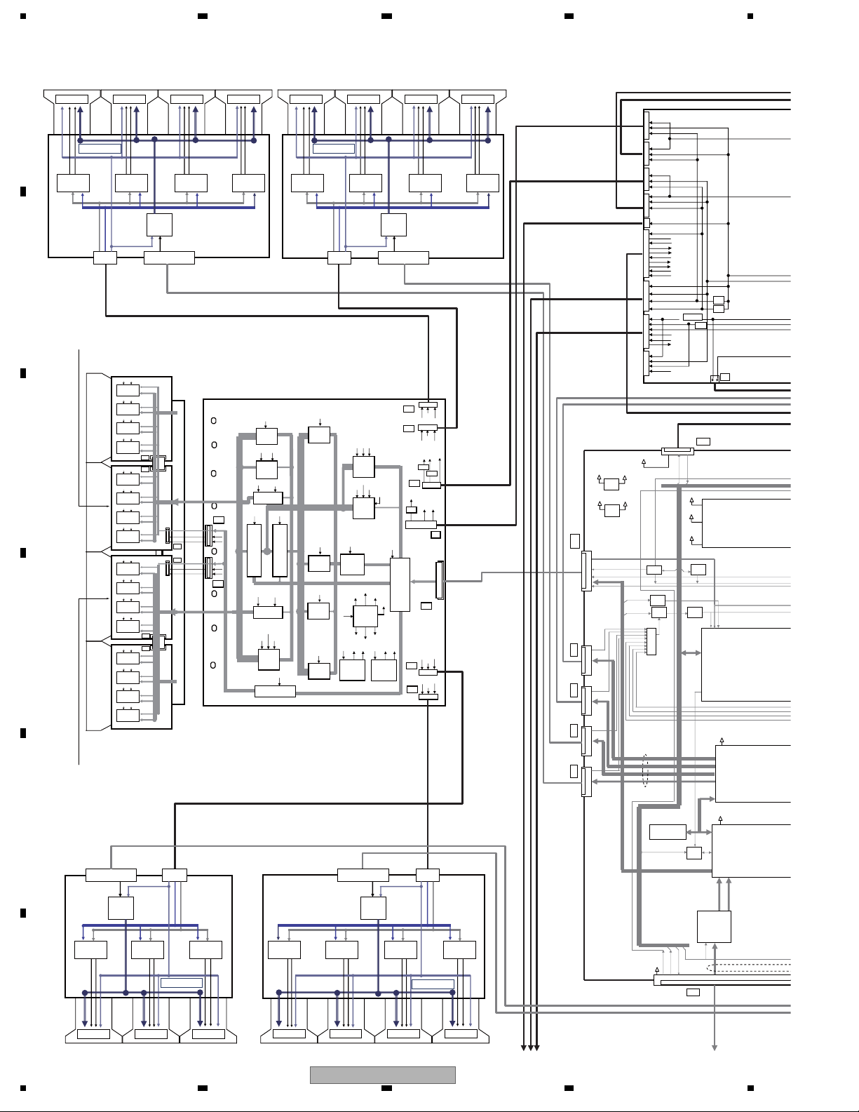
4. BLOCK DIAGRAM
4.1 OVERALL WIRING DIAGRAM (1/2)
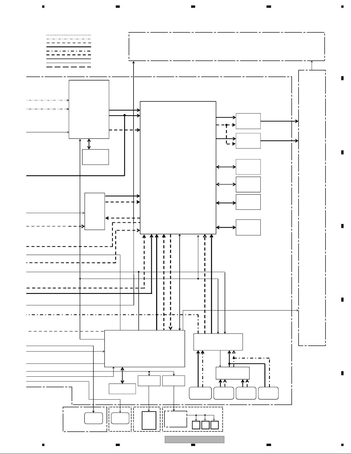
A
B
C
D
E
F
20
1 234
PDP-5010FD
Page 21

5678
A
B
C
D
E
When ordering service parts, be sure to refer to "EXPLODED
VIEWS and PARTS LIST" or "PCB PARTS LIST".
The mark found on some component parts indicates the
importance of the safety factor of the part. Therefore, when
replacing, be sure to use parts of identical designation.
PDP-5010FD
56
F
21
7
8
Page 22
1234
4.2 OVERALL WIRING DIAGRAM (2/2)
A
B
V+8V_AU
V+3_3V_A
V+3_3V_AU_D
C
D
E
F
22
1 234
PDP-5010FD
Page 23
5678
A
B
C
D
E
PDP-5010FD
56
F
23
7
8
Page 24
1234
4.3 OVERALL BLOCK DIAGRAM (1/2)
50F ADDRESS L ASSY
DRIVER IC
A
IC1651
RESONANCE
BLOCK
CLK / LE / HBLK / LBLK
R/G/B
V+60V
B
50F SCAN B ASSY
(HIGH-SIDE_LOW)
C
D
50F SCAN C ASSY
(LOW-SIDE_HIGH)
E
RESONANCE
BLOCK
VDDLS3 VADR2 VADR1VDDLS2 VDDLS1
F
DRIVER IC
IC1661
RESONANCE
BLOCK
IC1601
LVDS
V+3.3V
V+8V
AD2
CN1601
Receiver
50F SCAN A ASSY
(HIGH-SIDE_HIGH)
VH IC5V
Scan Signal
Scan IC
PSUS
IC2804
VH IC5V
Scan IC
IC2803
VH
IC5V
Scan IC
IC2802
VH
IC5V
Scan IC
IC2801
SA1
VH IC5V
SB2
Scan IC
IC2904
VH IC5V
Scan IC
IC2903
VH
IC5V
Scan IC
IC2902
VH IC5V
Scan IC
IC2901
VH
IC5V
Scan Signal
Scan IC
PSUS
IC3004
IC5V
VH
Scan IC
IC3003
IC5V
VH
Scan IC
IC3002
IC5V
VH
Scan IC
IC3001
SC2
VH
IC5V
SD1
Scan IC
IC3104
VH IC5V
Scan IC
IC3103
VH IC5V
Scan IC
IC3102
VH
IC5V
Scan IC
IC3101
50F SCAN D ASSY
(LOW-SIDE_LOW)
AD1
CN1802
AN/P BN/P
CN/P DN/P
CLKN/P
Receiver
VADR3
IC1801
LVDS
RESONANCE
BLOCK
V+3.3V
DRIVER IC
IC1671
RESONANCE
BLOCK
AN/P BN/P
CN/P DN/P
CLKN/P
AD1
CN1602
SB1
SC1
AD2
CN1801
V+60V
V+8V
CLK / LE / HBLK / LBLK
R/G/B
DRIVER IC
IC1681
VADR4VADR3
VDDLS3VADR2VADR1 VDDLS2VDDLS1
RESONANCE
BLOCK
50F Y DRIVE ASSY
PSUS
Y 2
Scan Signal
VH
VH
IC5V
IC5V
Scan Signal
VH
VH
IC5V
IC5V
Y 3
PSUS
RESONANCE
BLOCK
50F ADDRESS L ASSY
DRIVER IC
IC1651
VDDLS4
VC_P
VC_U
RESONANCE
VC_S
H-MSK
VC_U
RESONANCE
+16.5V
+16.5V
RST-D
BLOCK
VYPRST
PRST
BLOCK
BLOCK
BLOCK
VKNOFS1
KNOFS1
KNOFS3
BLOCK
Photo Coupler
RESONANCE
BLOCK
+16.5V
VC_S
L-MSK
+16.5V
VKNOFS3
IC5V
BLOCK
RESONANCE
BLOCK
VADR4 VADR3
VDDLS4
SUSOUT
DRIVER IC
IC1661
CLK / LE / HBLK / LBLK
R/G/B
RESONANCE
BLOCK
V+60V
V+3.3V
V+8V
AD2
CN1601
VSUS
SUS
BLOCK
MSK-S
BLOCK
BLOCK
BLOCK
VSUS
SUS
VSUS
SUS
VSUS
SUS
Gate Signal
PreDrive
VSUS
VKNOFS2
+16.5V
DC/DC
CONV.
+16.5V
+16.5V
SUS
VSNOFS
VC_S VC_U
15V
VC_S
KNOFS4
SOFT-G
BLOCK
VSNOFS
SNOFS
KNOFS2
BLOCK
VYPRST
MAIN
DC/DC
CONV.
VKNOFS3
VKNOFS4
VKNOFS2
Drive Signal
Drive Signal
Scan Signal
AD1
CN1602
AN/P BN/P
CN/P DN/P
CLKN/P
IC1601
LVDS
Receiver
RESONANCE
BLOCK
VDDLS3 VADR2 VADR1VDDLS2 VDDLS1
VC_S
Drive Signal
VKNOFS1
VKNOFS4
+16.5V
IC5V/VF
IC1601
Receiver
VH
IC5V VC_P+16.5V
DC/DC
CONV.
RESONANCE
LVDS
+5V
AN/P BN/P
CN/P DN/P
CLKN/P
AD1
CN1602
LOGIC
BLOCK
BLOCK
RESONANCE
Y 6
Y 7
Y 5
+5V
REG
+6.5V
Y 8
Y 9
V+3.3V
DRIVER IC
IC1671
VDDLS3VADR2VADR1 VDDLS2VDDLS1
BLOCK
+8V
VADR
+3.3V
+8V
+3.3V
VADR
VADR
+8V
+3.3V
REG
REG
+5.1V
12V
+16.5V
VSUS
Y 4
Y 1
VADR
+3.3V
+8V
VADR
+3.3V
+8V
AD2
CN1601
V+60V
V+8V
CLK / LE / HBLK / LBLK
R/G/B
VADR4VADR3
RESONANCE
BLOCK
DRIVER IC
IC1681
VDDLS4
RESONANCE
BLOCK
50F DIGITAL ASSY
V+3V_EE
V+2_5V_D
V+1_2V_D
1.2V
REG.
V+1_8V_D
1.8V
REG.
VH_UV_PD,
YDRIVE_PD,
YRESNC_PD,
YDD_CHV_PD,
IC5V_UV_PD
VOFS_ADJ,YPRST_ADJ,
XKNOFS1_2_ADJ,
XKNOFS3_ADJ,XKNOFS4_ADJ,
SCAN,YSUS
RELAY2
STOP_SQ
ADRPDMSK
LVDS
V+3VACTV
V+2_5V_D
D21
D16D15D14
D13
P1
P2P7P6P5
P4P8P9P12
DAC
Pulse
Width
MASK
OR
Flash Memory
IC3302
RELAY2
+16.5V
+12V
+6.5V
+5.1V
STB5.1V
STB3.3V
+35V
M_SW_DET
STB5.1V
+12V
STB3.3V
SCL,
SDA
ADR_PD1
+16.5V
+6.5V
VSUS
+16.5V
+6.5V
+12V
+5.1V
+60V
+12V
+5.1V
+16.5V
+5.1V
DRF_SW_B
M_SW_DET
EXT_PD
VSUS_ADJ
PS_PD
RELAY
DRF_B
AC_DET
PD_TRIG_B
AC_DET
US_SW
AC_DET
MSEL
SCL,SDA
UART
SECONDARY
T401
T402
IC202 152
Q203
+B for RELAY
DRIVE
P10
D24
TEMP1
Vsus_ADJ
PD_TRG_B, AC_DET, M_SW_DET
V+3_3V_D
V+2_5V_D
DC-DC
CONVERTER
BD8602FV
IC3801
V+1_1V_D
SCL,
SDA
DAC
SQ_NON
Pulse
Width
ADRS PD
UART
ODI_R, G, B
LVDS
Reciever
IC3201
INP_MUTE
D11
V+1_2V_D
V+3_3V_D
V+1_1V_D
V+1_8V_D
V+3_3V_D
ODI_SYNC
24
DRIVER IC
IC1871
DRIVER IC
IC1861
DRIVER IC
IC1851
50F ADDRESS S ASSY
DRIVER IC
IC1681
DRIVER IC
IC1671
DRIVER IC
IC1661
50F ADDRESS L ASSY
DRIVER IC
IC1651
ABC D
PDP-5010FD
1 234
Page 25
5678
T701
T901
+35V
T501
+16.5V
+12V
T101
RY102
+5_1V
RELAY
RELAY
+5_1V
PS_PWDN
PD
O
R
PD_MUTE
MODULE UCOM
M30620FCPGP
IC3601
LVDS
TRANSMITTER
PEG384B
IC3401
SUB-FILD CONV.
&
XY DRV SEQUENCE
PATTERN GEN.
PEG383B-K
IC3301
THEATER
LVDS
Reciever
IC3202
PRIMARY
Switching
Q701
Q702
Switching
Switching
Q901
Q902
Switching
Switching
Q501
Q502
Switching
IC101
Switching
OR
DRF_B
AND
XKOFS1_ADJ,XKNOFS2_ADJ
AND
V+3VACTV
EVI_SYNC
EVI_R, G, B
LVDS
POWER SUPPLY
UNIT
+390 V
PFC Q101
Q102
Q103
D109
D106
D108
RELAY
DRF_
EXT_PD
AND
PSW1
XSUSTN_PD,
XDD_CNV_PD,
XDRIVE_PD
PSW2
V+3VACTV
RESET
V+3V_D
RESET
RST2
AND
RST_SQ
PSIZE
LVDS
XSUS
RESETX
VD
D23
DRF_SW_B
PSW2
P11
SUS_MUTE
50F ADDRESS L ASSY
DRIVER IC
IC1651
D101
RESONANCE
BLOCK
CLK / LE / HBLK / LBLK
R/G/B
V+60V
V+8V
AD2
CN1601
DRIVER IC
IC1661
RESONANCE
BLOCK
V+3.3V
IC1601
LVDS
Receiver
AN/P BN/P
CN/P DN/P
CLKN/P
AD1
CN1602
DRIVER IC
IC1671
VDDLS3VADR2VADR1 VDDLS2VDDLS1
RESONANCE
BLOCK
VADR4VADR3
RESONANCE
50F ADDRESS S ASSY
DRIVER IC
IC1681
VDDLS4
BLOCK
DRIVER IC
IC1851
RESONANCE
BLOCK
CLK / LE / HBLK / LBLK
R/G/B
V+60V
V+8V
AD2
CN1801
DRIVER IC
IC1861
RESONANCE
BLOCK
V+3.3V
IC1801
LVDS
Receiver
CN1802
AN/P BN/P
CN/P DN/P
CLKN/P
AD1
DRIVER IC
IC1871
VADR3
RESONANCE
BLOCK
A
VDDLS3VADR2VADR1 VDDLS2VDDLS1
B
FHD POWER
SW ASSY
NEUTRAL
LIVE
F101
P3
AC INLET
SW2
SE1
PANEL
SENSOR
ASSY
50F X DRIVE ASSY
+60V +12V +5.1V
X 4
+60V
X 3
+8V
+60V
+8V
+3.3V
+3.3V
X 7
Gate Signal
+16.5V
X 5
PSUS
VXKOFS1
VXKOFS2
+16.5 VSUS
XPRST
+16.5
OFFSET
BLOCK
+12V
REGULATOR
+5.1V
REGULATOR
+16.5V
D22
VSUS +6.5V
X 2
+5V
Drive Signal
X 1
REGULATOR
+8V
+3.3V
+5V
+16.5V
SUS
PreDrive
PU
LOGIC
BLOCK
Drive Signal
RESONANCE
BLOCK
Drive Signal
D20D19
VPOFS
DC/DC
+16.5V
CONV.
D18
+60V +8V +3.3V
VPU
15V
+60V +8V +3.3V
VPOFS
OFFSET
Reg.
X 6
D17
: Wire harness
: FFC
VSUS
SUS
BLOCK
VSUS
SUS
BLOCK
+16.5
SOFT-D
VSUS
SUS
BLOCK
VSUS
SUS
BLOCK
PSUS
C
PSUS
D
E
AD1
CN1602
AN/P BN/P
CN/P DN/P
CLKN/P
IC1601
LVDS
Receiver
RESONANCE
BLOCK
VDDLS3 VADR2 VADR1VDDLS2 VDDLS1
RESONANCE
BLOCK
AD2
CN1601
V+3.3V
CLK / LE / HBLK / LBLK
R/G/B
V+60V
V+8V
RESONANCE
BLOCK
RESONANCE
BLOCK
VADR4 VADR3
VDDLS4
AD1
CN1602
AN/P BN/P
CN/P DN/P
CLKN/P
IC1601
LVDS
Receiver
RESONANCE
BLOCK
VDDLS3 VADR2 VADR1VDDLS2 VDDLS1
RESONANCE
BLOCK
AD2
CN1601
V+3.3V
CLK / LE / HBLK / LBLK
R/G/B
V+60V
V+8V
RESONANCE
BLOCK
RESONANCE
BLOCK
VADR4 VADR3
VDDLS4
F
DRIVER IC
IC1681
DRIVER IC
IC1671
DRIVER IC
IC1661
DRIVER IC
IC1651
50F ADDRESS L ASSY
PDP-5010FD
56
DRIVER IC
IC1681
DRIVER IC
IC1671
50F ADDRESS L ASSY
7
DRIVER IC
IC1661
DRIVER IC
IC1651
25
8
Page 26
1234
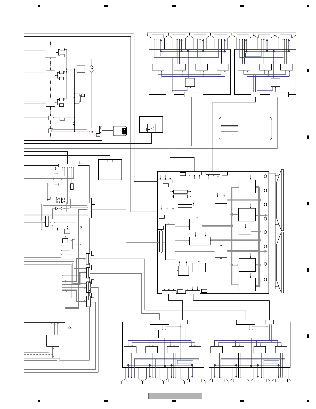
4.4 OVERALL BLOCK DIAGRAM (2/2)
Modulator
U6001
AXF1171
(Frontend)
U6101
AXF1178
(Frontend)
REM
IC6102
7W66FU
I2C_TUNER_SCL
I2C_TUNER_SDA
IR_REPEATER
Antenna B
A
TANSHI ASSY
Input
Antenna A
Input
MAIN ASSY
AIR_R
AIR_L
B
AUDIO_OUT_L/R
SW_L/R
L/R
L/R
L/R
L/R
AUDIO Output
SUB WOOFER
Input 1
Input 2
PC Input
Input 4 HDMI
V
Y/C
V
Y/Pb/Pr
SIF_OUT
AIR2_V
AIR1_V
V
IC6002
74HC4066
IC6001
LA72702NVA
IC4601
R2S11006FT
(AVSW)
VBI_Y
SIF_SW
SDA_AV5
SCL_AV5
SDA_AV5
SCL_AV5
FE_I2C_SEL
SDA_AV5
SCL_AV5
DA_GY
C
IC9101
MAP5601M
(MAP)
L/R
Input 5 HDMI
GY_VDEC
Input2_Y/Pb/Pr
L/R
Input 3
SIDE IO ASSY
PC Input
D
SDA_AV
SCL_AV
I2S_BCLK_DTV
I2S_LRCLK_DTV
I2S_SDATA_DTV
SPDIF_DTV
I2S_BCLK_HDMI
I2S_LRCLK_HDMI
I2S_SDATA_HDMI
SPDIF_HDMI
SR_OUT
V
TXD_SR+
RXD_SR+
REM
PC_RGB
PC_H/V
Input3_Y/Pb/Pr
IC4701
R2S11001FT
(RGBSW)
DA_RCR
DA_BCB
DA_GY
CLP_RGB
SDA_AV5
SCL_AV5
E
IC8301
AGC1037(IF UCOM)
IC9201
TAS5122DCA-TBB
(D-AMP)
RS232C
REM
REM
FHD IR ASSY
DS_IF_N
DS_IF_P
TXD/RXD
232C_DET
IC7001
TC90173FG
KEY
F
POD Card
26
KEY_AD1/AD2
SIDE KEY ASSY
POD ASSY
IC6301
BCM3517
PDP-5010FD
IC6401
BCM7038
USB
1 234
Page 27
MAIN_Y/C
SUB_Y/C
SDA_MB
SCL_MB
5678
: Analog Audio signal
IC4801
CM0048BF
(VDEC)
REQ_VDEC
RST_ASIC
HY57V161610FTP
: Analog Video signal
: Component signal
: Digital Video signal
: Digital Audio signal
: Synchronized signal
: Data signal
: Control signal
: RF signal
VD3,4
HD3,4
MD_VDEC
MA_VDEC
MCTRL
IC4802
(SDRAM)
DIN4
DIN3
M_SW_DET
AC_DET_DRV
POWER SUPPLY UNIT
IC8001
PD6568A-K
(ARIA)
RA_0
GA_0
BA_0
VD_0
HD_0
RB_0
GB_0
BB_0
MA_ARIA_A
MD_ARIA_A
IC4101
BU8254KVT
(LVDS)
IC4102
BU8254KVT
(LVDS)
IC8201
EDD1232ABBH
(128Mbit DDR)
DIGITAL
ASSY
A
B
SDA_AV
SCL_AV
RCR_AD
BCB_AD
GY_AD
LED_ON1/ON2/OFF
TXD_IF/RXD_IF
RST3
TXD/RXD_DT
IC5001
AD9985KSTZ
(ADC)
TRAP SW
DIN5_RCR
DIN5_BCB
DIN5_GY
HD5
HD_PLL
HOLD_PLL
CLP_AD
INT_HD1/VD1
EXT_HD1/VD1
A0 to 19
DQ0 to 15
IC8402
AGC1039-
(FLASH)
IC8401
UPD61123F1
(EMMA2SV)
FAN_ON1/CONT1
PQ200WNA1ZPH
(FAN CONTROL)
VD1
HD1
IC4310
DIN7_BCB/RCR/GY
DIN7_ALPHA
DIN1_DVO
HD7
FAN_ON2/CONT2
PQ200WNA1ZPH
(FAN CONTROL)
VD7
IC4303
HD7_0
VD7_0
MA_ARIA_B
MD_ARIA_B
MA_ARIA_C
MD_ARIA_C
EXD_ARIA
EXA_ARIA
RXD_IC3
TXD_IC3
RST_ASIC
VD6
HD6
DIN6_BCB
DIN6_RCR
DIN6_GY
IC8202
EDD1232ABBH
(128Mbit DDR)
IC8203
EDD1232ABBH
(128Mbit DDR)
IC8204
AGC104 9-
AGC104 9
(16Mbit Flash)
C
D
TXD_MD
RXD_MD
REQ_MD
RST_ASIC
HDMI_INT
SCL_MB
SDA_MB
E
Input 4
HDMI
IC5201
SII9025CTU
(HDMI RX)
DSDA_1
Input 5
HDMI
DSCL_1
IC5101
CXB1442
(HDMI SW)
Input 6
HDMI
Input 7
HDMI
LED
50 FHD LED ASSY
TRAP SW
FAN
FHD FAN
CONNECT
ASSY
FAN FAN FAN
PDP-5010FD
56
F
27
7
8
Page 28
1234
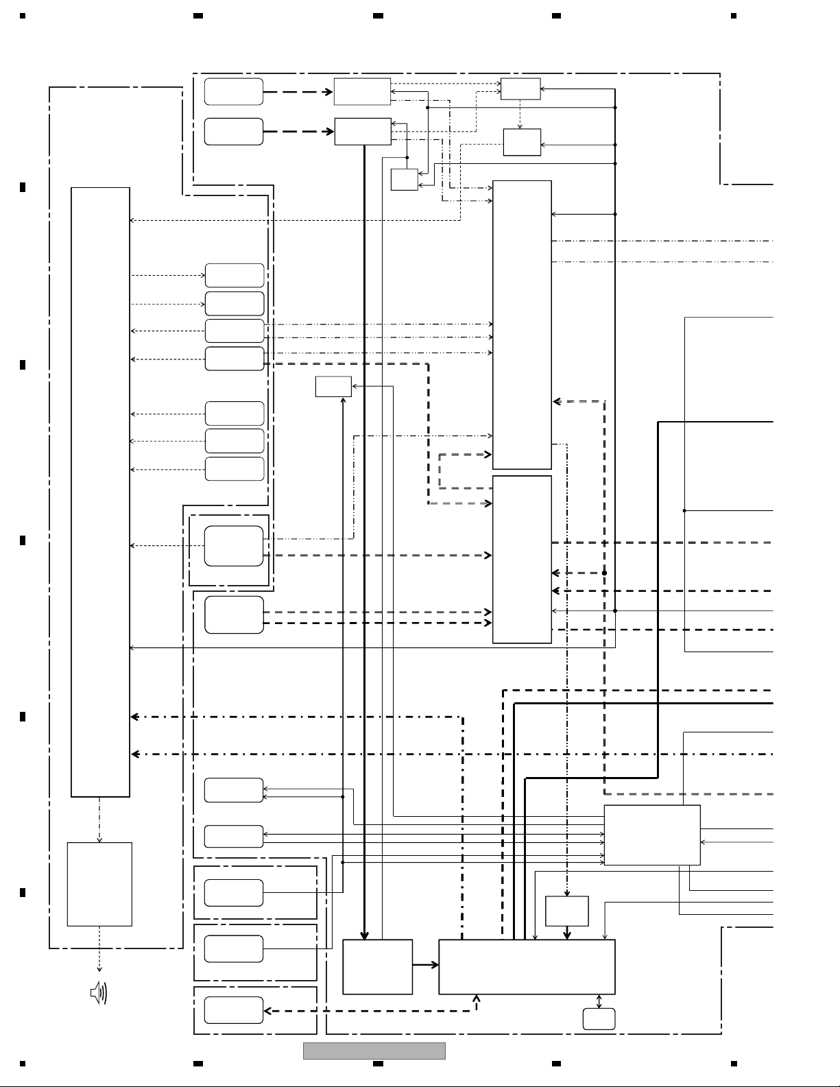
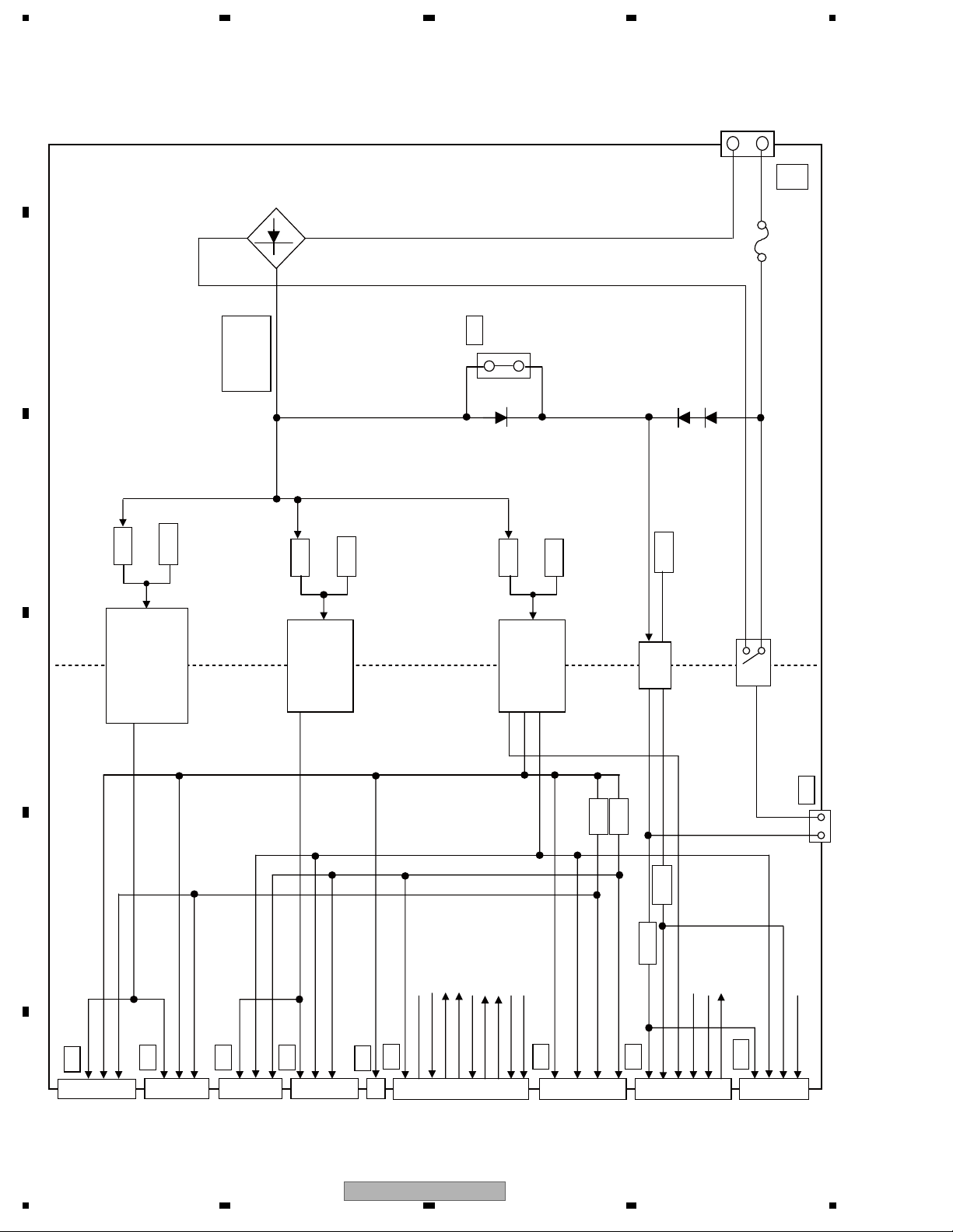
4.5 POWER SUPPLY UNIT
A
POWER SUPPLY UNIT
D101
B
Q102
Q103
P3
LIVE
NEUTRAL
F101
P11
PFC Q101
D108
D106
D109
+390V
C
Q701
Switching
Q702
Switching
Q901
Switching
Q902
Switching
Q501
Switching
Q502
Switching
IC101
Switching
PRIMARY
RY102
T101
D
T701
T901
SECONDARY
T501
+35V
+16.5V
+12V
T401
T402
P10
+B for Relay Drive
Q203
E
IC202
+12V
+60V
+12V
+5.1V
P7
P2
+6.5V
+16.5V
VSUS
+16.5V
+6.5V
P1
F
28
1 234
P6
+5.1V
+16.5V
+5.1V
P4
P5
PDP-5010FD
VSUS_ADJ
DRF_SW_B
EXT_PD
M_SW_DET
PS_PD
RELAY
DRF_B
AC_DET
PD_TRIG_B
+12V
+16.5V
P8
+6.5V
+5.1V
STB5.1V
STB3.3V
P9
M_SW_DET
+35V
US_SW
AC_DET
+12V
STB5.1V
P12
AC_DET
STB3.3V
Page 29
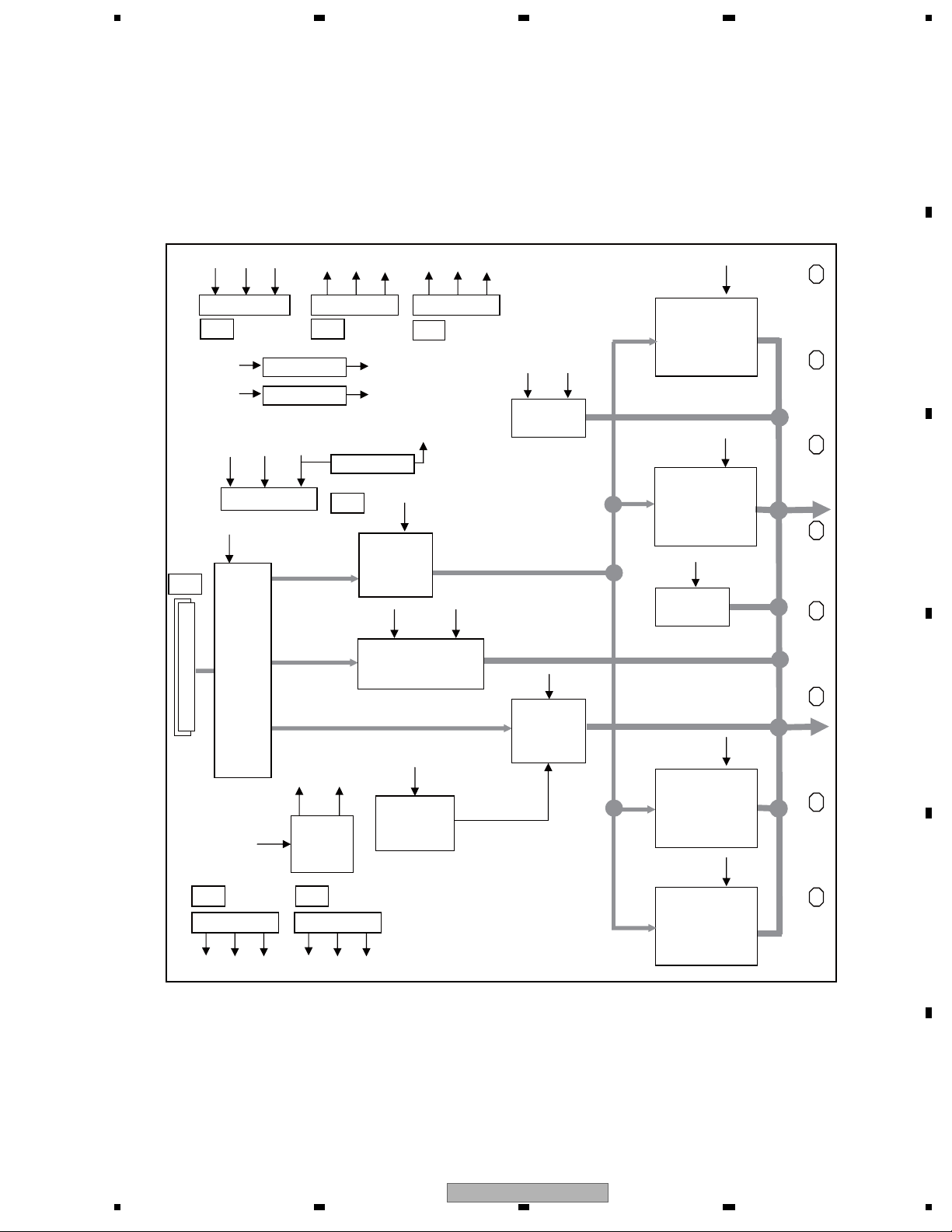
5678
4.6 50F X DRIVE ASSY
50F X DRIVE ASSY
+60V +12V +5.1V
X 7
+12V
+5.1V
VSUS +6.5V
REGULATOR
+16.5V
+60V
X 4
REGULATOR
REGULATOR
+8V
+3.3V
+8V
+3.3V
+60V
X 3
+5V
+8V
+3.3V
A
VSUS
B
SUS
BLOCK
+16.5 VSUS
XPRST
VSUS
X 1
X 6
+5V
LOGIC
BLOCK
+16.5V
X 2
Drive Signal
Drive Signal
Drive Signal
VPOFS
VPU
15V
DC/DC
CONV.
X 5
+16.5V
SUS
PreDrive
PU
RESONANCE
BLOCK
VPOFS
OFFSET
Reg.
Gate Signal
+16.5V
VXKOFS1
VXKOFS2
PSUS
+16.5
OFFSET
BLOCK
SUS
BLOCK
+16.5
SOFT-D
SUS
BLOCK
SUS
BLOCK
VSUS
VSUS
PSUS
C
D
PSUS
E
+60V +8V +3.3V
+60V +8V +3.3V
PDP-5010FD
56
F
29
7
8
Page 30
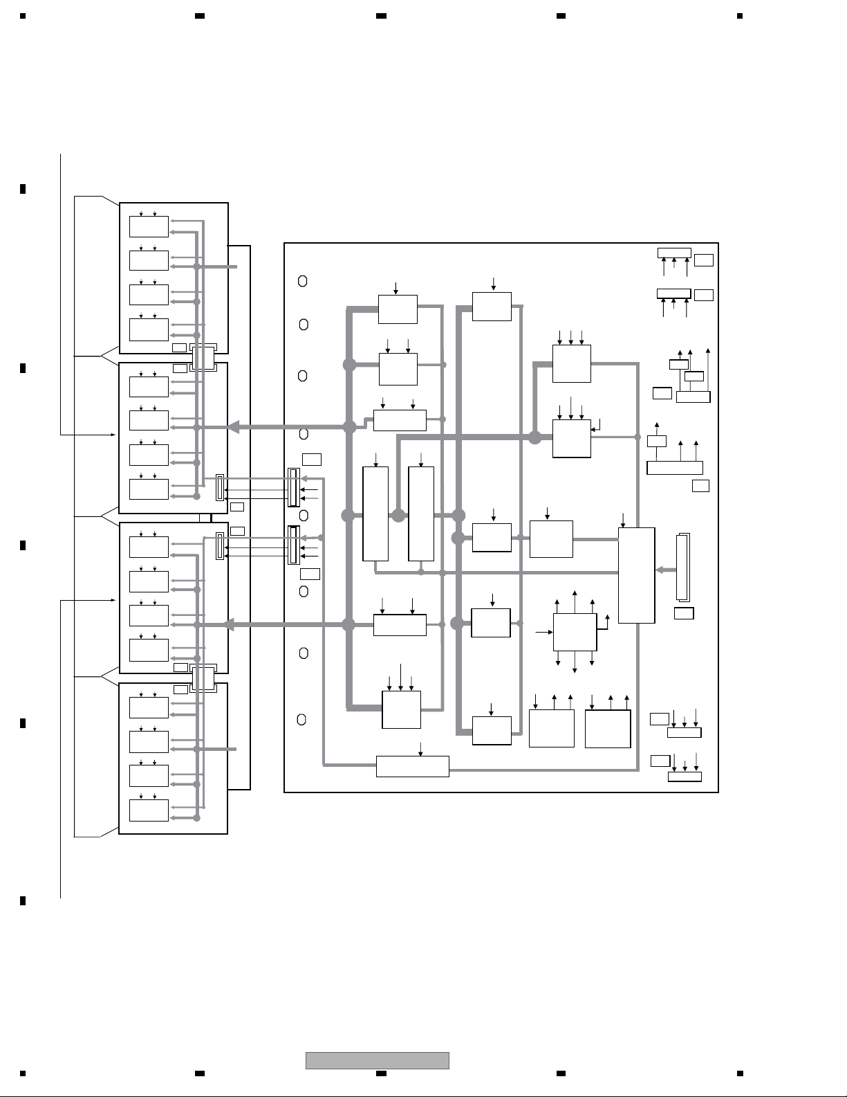
1234
4.7 50F Y DRIVE, 50F SCAN A, B, C and D ASSYS
A
50F SCAN B ASSY
(HIGH-SIDE_LOW)
50F SCAN A ASSY
(HIGH-SIDE_HIGH)
VH IC5V
Scan Signal
Scan IC
PSUS
IC2804
VH IC5V
Scan IC
IC2803
VH
B
C
D
E
IC5V
Scan IC
IC2802
VH
IC5V
Scan IC
IC2801
VH IC5V
Scan IC
IC2904
VH IC5V
Scan IC
IC2903
VH
IC5V
Scan IC
IC2902
VH IC5V
Scan IC
IC2901
VH
IC5V
Scan IC
IC3004
IC5V
VH
Scan IC
IC3003
IC5V
VH
Scan IC
IC3002
IC5V
VH
Scan IC
IC3001
VH
IC5V
Scan IC
IC3104
VH IC5V
Scan IC
IC3103
VH IC5V
Scan IC
IC3102
VH
IC5V
Scan IC
IC3101
SA1
SB2
Scan Signal
PSUS
SC2
SD1
SB1
SC1
50F Y DRIVE ASSY
PSUS
PSUS
Y 3
Y 2
VH
IC5V
VH
IC5V
Scan Signal
VH
IC5V
Scan Signal
VH
IC5V
+16.5V
RST-D
BLOCK
VC_P
PRST
BLOCK
VC_U
RESONANCE
BLOCK
VC_S
H-MSK
VC_U
RESONANCE
BLOCK
VKNOFS1
+16.5V
KNOFS1
KNOFS3
BLOCK
Photo Coupler
VYPRST
+16.5V
VC_S
L-MSK
+16.5V
VKNOFS3
IC5V
BLOCK
VSUS
SUS
BLOCK
MSK-S
SUSOUT
VSUS
SUS
BLOCK
VSUS
SUS
BLOCK
VSUS
SUS
BLOCK
+16.5V
+16.5V
Gate Signal
+16.5V
SUS
PreDrive
VSNOFS
VSUS
VKNOFS2
VC_S VC_U
15V
DC/DC
CONV.
Scan Signal
VC_S
VKNOFS4
KNOFS4
SOFT-G
BLOCK
VSNOFS
SNOFS
KNOFS2
BLOCK
VYPRST
MAIN
DC/DC
CONV.
VKNOFS3
VKNOFS2
VC_S
Drive Signal
Drive Signal
Drive Signal
VKNOFS1
VKNOFS4
+16.5V
IC5V/VF
DC/DC
CONV.
Y 6
+8V
VADR
+3.3V
Y 7
+8V
+3.3V
VADR
VADR
+8V
+3.3V
REG
REG
+5.1V
12V
Y 5
+5V
+16.5V
REG
VSUS
+6.5V
Y 4
+5V
LOGIC
BLOCK
VH
IC5V VC_P+16.5V
Y 8
Y 9
+3.3V
+3.3V
Y 1
VADR
+8V
VADR
+8V
50F SCAN D ASSY
(LOW-SIDE_LOW)
50F SCAN C ASSY
(LOW-SIDE_HIGH)
F
30
1 234
PDP-5010FD
Page 31

5678
4.8
POWER SUPPLY BLOCK of 50F X, Y DRIVE and 50F SCAN A, B, C and D ASSYS
A
50F Y DRIVE ASSY
Logic
Pre
SUS-B
drive
FET
Pre
SUS-G
drive
FET
Pre
SUS-U
drive
IGBT
Pre
SUS-D
drive
IGBT
Pre
HMSK
drive
FET
Pre
LMSK
drive
FET
Pre
YPRST
drive
FET
Pre
SNOFS
drive
FET
Pre
YKOFS
drive
1
FET
Pre
YKOFS
drive
2
FET
Pre
YKOFS
drive
3
FET
Pre
YKOFS
drive
4
FET
Pre
RST-D
drive
FET
VF1
VF2
VF3
IC5V
VH
VF
DC/DC
Conv.
VPOFS
VXKOFS1
Reg.
VXKOFS2
Reg.
to
ADDRESS ASSY
9.0V 12V
5.0V 6.5V
to
ADDRESS ASSY
3.3V 5.1V 3.3V 5.1V
3.3V
Reg.IC
5.0V
15V
DC/DC Conv.
IC5V
DC/DC Conv.
DC/DC
Conv.
VYPRST
Reg.
VSNOFS
Reg.
VYKOFS
12
Reg.
9V
9V
Reg.IC
5V
Reg.IC
12V
6.5V
16.5V
VSUS
from
POWER
SUPPLY
50F X DRIVE ASSY
Logic
SUS-B
FET
SUS-G
FET
SUS-U
IGBT
SUS-D
IGBT
XPRST
FET
XSOFT-G
FET
XKOFS1
FET
XKOFS2
FET
drive
drive
drive
drive
drive
drive
drive
drive
Pre
Pre
Pre
Pre
Pre
Pre
Pre
Pre
5.0V
VXKOFS1
VXKOFS2
Note:
VYKOFS
3
Reg.
VYKOFS
4
Reg.
VYPRST, VSNOFS, VYKOFS12, VYKOFS3, VYKOFS4
VXKOFS1 and VXKOFS2 voltages are electrical volume controls.
3.3V
Reg.IC
9V
Reg.IC
5V
Reg.IC
B
16.5V
VSUS
from
POWER
SUPPLY
C
D
Pre
SOFT-G
drive
FET
Scan
Logic
IC5V VH
Scan IC
50F SCAN A, B, C, D ASSYS
56
PDP-5010FD
E
F
31
7
8
Page 32

1234
4.9 50F ADDRESS L and S ASSYS
A
50F ADDRESS L ASSY
DRIVER IC
IC1651
CLK / LE / HBLK / LBLK
R/G/B
B
RESONANCE
BLOCK
V+60V
C
AD2
CN1601
V+3.3V
V+8V
DRIVER IC
IC1661
RESONANCE
BLOCK
IC1601
LVDS
Receiver
AN/P BN/P
CN/P DN/P
CLKN/P
AD1
CN1602
DRIVER IC
IC1671
VDDLS3VADR2VADR1 VDDLS2VDDLS1
RESONANCE
BLOCK
DRIVER IC
IC1681
VADR4VADR3
RESONANCE
BLOCK
VDDLS4
50F ADDRESS S ASSY
DRIVER IC
D
E
IC1851
CLK / LE / HBLK / LBLK
R/G/B
RESONANCE
BLOCK
DRIVER IC
IC1861
RESONANCE
BLOCK
IC1801
LVDS
V+60V
F
V+3.3V
V+8V
Receiver
AD2
CN1801
CN1802
VADR3
AN/P BN/P
CN/P DN/P
CLKN/P
AD1
DRIVER IC
IC1871
VDDLS3VADR2VADR1 VDDLS2VDDLS1
RESONANCE
BLOCK
32
PDP-5010FD
1 234
Page 33

5678
4.10 50F DIGITAL ASSY
50F DIGITAL ASSY
V+3V_EE
V+2_5V_D
V+2_5V_D
D21
D16D15D14
V+1_2V_D
1.2V
REG.
V+1_8V_D
1.8V
REG.
VH_UV_PD,
YDRIVE_PD,
YRESNC_PD,
YDD_CHV_PD,
IC5V_UV_PD
VOFS_ADJ,YPRST_ADJ,
XKNOFS1_2_ADJ,
XKNOFS3_ADJ,XKNOFS4_ADJ,
SCAN,YSUS
RELAY2
STOP_SQ
ADRPDMSK
OR
DAC
Pulse
Width
MASK
TEMP1
SCL,SDA
PD_TRG_B, AC_DET, M_SW_DET
V+3_3V_D
V+2_5V_D
V+1_1V_D
SCL,
SCL,
SDA
SDA
SQ_NON
Pulse
Width
ADR_PD1
CONVERTER
DAC
ADRS PD
Vsus_ADJ
DC-DC
BD8602FV
IC3801
MODULE UCOM
M30620FCPGP
PS_PWDN
O
R
PD_MUTE
IC3601
RELAY
+5_1V
+5_1V
RELAY
OR
DRF_B
AND
PD
XKOFS1_ADJ,XKNOFS2_ADJ
AND
V+3VACTV
RELAY
PSW1
PSW2
RESET
RST2
RST_SQ
D23D24
EXT_PD
V+3VACTV
RESET
V+3V_D
DRF_
AND
AND
DRF_SW_B
XSUSTN_PD,
XDD_CNV_PD,
XDRIVE_PD
PSW2
SUS_MUTE
A
B
D22
C
D13
LVDS
Flash Memory
IC3302
UART
V+1_2V_D
V+3_3V_D
TRANSMITTER
V+1_1V_D
V+1_8V_D
V+3_3V_D
SUB-FILD CONV.
XY DRV SEQUENCE
PATTERN GEN.
ODI_R, G, B
ODI_SYNC
LVDS
Reciever
IC3201
LVDS
PEG384B
IC3401
&
PEG383B-K
IC3301
THEATER
EVI_R, G, B
LVDS
Reciever
IC3202
PSIZE
D20D19
D
D18
LVDS
D17
XSUS
RESETX
E
VD
EVI_SYNC
INP_MUTE
RELAY2
MSEL
V+3VACTV
UART
LVDS
D11
PDP-5010FD
56
F
33
7
8
Page 34

1234
4.11 MAIN ASSY (DTV BLOCK DIAGRAM)
A
B
C
D
[CN4005/CN4006]
CIMaX sp2
[IC7302]
[IC6602]
SDRAM
[IC6603]
2
[IC6604]
[IC6605]
To POD ASSY
Logic
Circuit
SLICER
[IC7001 ]
SDRAM
256Mbit
56M bit
SDRAM
256Mbit
SDRAM
2
56
Mbit
G-Link
OOB_Data
EBI BUS
VBI
HSX_0
I2C0
TS
MEMORY BUS
FLASH
32M
[IC6902 ]
.
.
.
To TANSHI ASSY
[CN4001]
I2S out
1Chip System IC
BCM7038KPB1G-B2-K
[IC6401]
SPDIF out
UARTA
SAW
filter
EEPROM
64Kbit
IF SW
[IC6103]
I2C1
IF AGC
TS0
DVO
[12bit]
YUV(656)
[8bit]
VBI_Y
AGC
RF
Tuner
[U6101]
QPSK IF
QPSK IF
Down Conv.
[IC6201]
Demodulate IC
BCM3517
KQLGB0-K
[IC6301]
I2C_TUNER_SCL
AIR1_V
IF
I2C_TUNER_SDA
I2C SW
[IC6102]
SCL_AV5
SDA_AV5
To AV_SW
From EMMA2
To ARIA
From VDEC
From AV_SW
E
F
34
PDP-5010FD
1 234
Page 35

5678
A
B
C
D
E
PDP-5010FD
56
F
35
7
8
Page 36

1234
4.12 POWER SUPPLY BLOCK of MAIN ASSY
A
SW REG CONTROLED BY RELAY
V
V+35
Discrete
30V-REG
(V+30V_ANT_A)
Discrete
B
30V-REG
(V+30V_ANT_B)
for Tuner for Main BoardFAN
V+30V_ANT_A
for Tuner
V+30V_ANT_B
V+12
V
IC4310
Variable REG
(FAN_VCC1)
PQ200WNA1ZPH
IC4303
Variable REG
(FAN_VCC2)
PQ200WNA1ZPH
IC4301
8V-LEG (Variable REG)
(V+8V_AIR/AU/A/A2
/DSP)
PQ200WNA1ZPH
+6_
V
5V
IC4305
5V-REG
FAN_VCC1
for FHD Panel FAN
FAN_VCC2
for SW, Audio, Ant_A,
Ant_B, DSP
V+8V_A
V+8V_A_AV
V+8V_A_DSP V+5V_A2_RGB
(V+5V_ANT_A)
NJM2846DL3-05
IC4307
5V-REG
(V+5V_A)
NJM2846DL3-05
for Ant_A, QPSK, Ant_B, MPX
for AV_SW, RGB_SW, HDMIROM,
7038EEPROM, 7038IIC A/D
V+5V_ANT_A
V+5V_ANT_A_SAW
V+5V_ANT_A_QPSK
V+5V_ANT_B
V+5V_ANT_B_MPX
V+5V_A_AV
V+5V_A_7038
V+5V_A2_HDMI_ROM
C
STBY SW REG
V+5_1V_STB V+3_3V_STB
V+5_1V_STB
for IF U COM
V+3_3V_STB
IC4309
DD com.
(V+5V_USB/DLNA)
R1224N102H/
RTQ040P02
for USB, DLNA
IC6402
Switch IC
(V+5V_USB)
R5523H001B
V+5V_HNM
V+5V_USB
D
Filter
(V+3_3V_UCOM)
Q4421
FET Switch
(V+3_3V_UCOM)
RTQ040P02
for EMMA
V+3_3V_UCOM
V+3_3V_UCOM_ROM
E
2ch
DD com.
IC4308
Variable REG
(POD_VPP)
PQ200WNA1ZPH
IC4306
DD com.
(POD_VCC)
R1224N102H/
RTQ040P02
LC Filter
(V+5V_D)
for POD VPP
POD_VPP (5.0V/3.3V)
for POD_VCC
POD_VCC (3.3V)
V+5V_D
LTC3407
IC4501
DD com.
(V+2_5V_UCOM)
LTC3407-2
IC4501
DD com.
(V+1_5V_UCOM)
LTC3407-1
for EMMA
for EMMA
V+2_5V_UCOM
V+2_5V_UCOM_DDR
V+1_5V_UCOM
F
IC4401
3.3V-REG
(V+3_3V_A)
NJM2846DL3-33
IC4404
DD com.
(V+1_2V_D)
LTC3416
Q4416
FET Switch
(V+3_3V_A_VDEC)
RTQ040P02
for 7038, 3517
V+3_3V_A_ADC
V+3_3V_A_VDEC
V+1_2V_D_7038
V+1_2V_D_3517
36
PDP-5010FD
1 234
Page 37

5678
A
V+5_1V
IC4403
3ch DD com.
(V+3_3V_D)
BD8602FV-1/
SP8M4
for 7038, 3517, POD, DT_D, DSP, ARIA, LVDS,
VDEC_D, ADC, HDMI, HDMI_SW, VBI
Q4515
FET Switch
(V+3_3V_D2)
RTQ040P02
V+3_3V_D_DSP V+3_3V_UCOM_VBI
V+3_3V_D_ADC V+3_3V_D_7038
Q4415
FET Switch
(V+3_3V_D2)
RTQ040P02
3ch DD com. BD8602FV
Q4404
FET Switch
(V+3_3V_D4)
RTQ040P02
V+3_3V_A2_7038
V+3_3V_A2_DSP
V+3_3V_D_7038_ROM
V+3_3V_D_3517
V+3_3V_D_POD
for VDEC_D, HDMI, HDMI_SW
V+3_3V_D2_VDEC
V+3_3V_D2_VDEC_RAM
Q4418
FET Switch
(V+3_3V_D3)
RTQ045N03
V+3_3V_D4_ARIA V+1_8V_A_HDMI
V+3_3V_D4_ARIA_ROM
V+3_3V_D3_HDMI
V+3_3V_D3_HDMISW
IC4405
1.8V-REG
(V+1_8V_A)
NJM2846DL3-18
B
C
IC4403
3ch DD com.
(V+2_5V_D)
BD8602FV-3/
SP8M4
IC4403
3ch DD com.
(V+1_2V_D2)
BD8602FV-3/
RSS100N03
RSS090P03
for 7038, 3517, ARIA, VBI
V+2_5V_D_7038 V+1_8V_A_VDEC
V+2_5V_D_7038_DDR
V+2_5V_D_3517
Q4411
FET Switch
(V+2_5V_D2)
RSS100N03
Q4514
FET Switch
(V+3_3V_D2)
RTQ040P02
IC4106
for ARIA
V+1_2V_D2_ARIA
1.5V-REG
(V+1_5V_VDEC)
NJM2886DL3-15
V+3_3V_D4_LVDS
V+2_5V_D2_ARIA
V+2_5V_D2_ARIA_DDR
V+2_5V_UCOM_VBI
V+1_5V_UCOM_VBI
Q4422
FET Switch
(V+1_8V_A_VDEC)
MCH3406
D
E
F
PDP-5010FD
56
37
7
8
Page 38

1234
4.13 TANSHI ASSY
A
TANSHI ASSY
IO6
+16.5V
IO5
+3.3V+8V
B
+16.5V
PWM
DIGITAL AMP IC
IC9201
TAS5122DCA
+16.5V +12V
REGULATOR
IC9181
NJM78M12DL1A
MAP IC
IC9101
MAP5601M
LPF
+3.3V
REGULATOR
IC9191
NJM2846DL3
+3.3V
OUTPUT(AUDIO)
INPUT(AUDIO)
C
SCL_AV
SDA_AV
RST_MSP
SPDIF_DTV
R_OUT+
R_OUT-
L_OUT-
L_OUT+
DC
DETECT
BLOCK
OTW
A_NG_B
I2S_DTV
SPDIF_HDMI
+1.8V
OPT_OUT
IO3
+1.8V
OPTICAL OUT
SUB WOOFER OUT
AUDIO OUT
INPUT1
INPUT2
INPUT3
INPUT4
INPUT5
PC AUDIO
AIR
INPUT3(AUDIO,CVBS)
INPUT(VIDEO)
AIR
INPUT3(YPbPr)
HP
IO4
for MAIN ASSY
IO2
for SIDE IO ASSY
IO1
for SIDE IO ASSY
for MAIN ASSY
IO8
D
IO9
L OUTR OUT
SP TERMINAL
E
F
38
1 234
PDP-5010FD
Page 39

5678
4.14 50FHD LED and FHD IR ASSYS
A
FAN FAN FAN
M4
USB FAN
POWER SUPPLY UNIT
FA3 FA4 FA5
FA1
FHD FAN CONNECT ASSY
M5
MAIN ASSY
M34
M33
M9
B
C
C2
C1
POD ASSY
D
IO5
D11 P8 P9
M11
M15
DIGITAL ASSY
LED_TIMER
LED_OFF
LED_ON M1 M3 M2 M21
50FHD LED ASSY
FHD IR ASSY
PDP-5010FD
56
M8
M6
IO3
IO4
IO_AUDIO ASSY
E
F
FHD RLS ASSY
39
7
8
Page 40

1234
4.15 POWER SUPPLY BLOCK of FHD RLS and SIDE KEY ASSYS
A
FHD RLS ASSY
B
V+3_3V_UCOM
OP AMP
IC9781
CN9781
C
MAIN ASSY
MM3012XN
RLS
IC9782
AMS114YD01
D
SIDE KEY ASSY
V+3_3V_STB
KEY
S9501 to S9507
E
CN9501
MAIN ASSY
F
40
1 234
PDP-5010FD
Page 41

5678
5. DIAGNOSIS
5.1 POWER SUPPLY OPERATION
5.1.1 LED DISPLAY INFORMATION
LED Pattern
AC OFF or
Main power switch OFF
Standby power
management
Power ON
Power-down
Shutdown
No digital adjustment
data copied for backup
In the process of
rewriting the program
of the microcomputer
During factory
operation
During DTV Module
software downloading
Downloading of DTV
Module software is finished
normally.
Downloading of DTV
Module software is
abnormally finished.
Trap switch
Blue
Red
Orange
Blue
Red
Orange
Blue
Red
Orange
Blue
Red
Orange
Blue
Red
Orange
Blue
Red
Orange
Blue
Red
Orange
Blue
Red
Orange
Blue
Red
Orange
Blue
Red
Orange
Blue
Red
Orange
Blue
Red
Orange
Once
500 mS
500 mS
Once
200 mS
100 mS
100 mS
100 mS
100 mS
500 mS 500 mS 500 mS 500 mS 500 mS 500 mS 500 mS
500 mS 500 mS 500 mS 500 mS 500 mS 500 mS 500 mS
Twice n times
Twice n times Once
POWER ON STANDBY SLEEP
LED Pattern / RemarksLEDState
Lightins out
Lightins out
Lightins out
Lightins out
Always lighting
Lightins out
Always lighting
Lightins out
Lightins out
2.5 S
Lightins out
2.5 S
Lightins out
Always lighting
Lightins out
Lightins out
Always lighting
Always lighting
Lightins out
A
B
Once
C
D
E
PDP-5010FD
56
F
41
7
8
Page 42

1234
5.1.2 POWER ON SEQUENCE
A
REM
infrared
receiver
B
Side Keys
MOD
Microcomputer
IC3151
Power MOD
4
RELAY Control
Inv. Amp
Q9731
KEY_1
REM
C
SR_IN
Inv. Amp
Q4105
Microcomputer
1
KEY_2
1
IF
IC8301
Inv. Amp
Q8302
SR_OUT
TXD_IF
RXD_IF
CE_IF
REQ_IF
BUSY_IF
TXD_MD
RXD_MD
REQ_MD
2
3
MAIN
Microcomputer
IC8401
D
SR OUT Jack
JA9404
1 : The remote control (or KEY) signal is input to the IF microcomputer.
2 : The IF microcomputer sends the operation data of the remote control unit (or KEY) to the main microcomputer.
3 : The main microcomputer issues a startup command (PON) to the MOD microcomputer.
4 : The relay is controlled with logical OR interpretation of control signals by the main microcomputer and
module (MOD) microcomputer.
E
F
42
PDP-5010FD
1 234
Page 43

5678
5.1.3 DETAILS OF POWER ON SEQUENCE
Power supply status - AC off
A
Microcomputer
output port state
IF: ACTIVE
Main: RELAY2
Main: PSW1
Module: RELAY
Module: DRF_B
Microcomputer
input port state
Main: RST4
Main: RST2
Module: RST2
IR/Key/
OFF
232C
OFF
OFF
OFF
OFF
OFF
LED
EEPROM
Short
ACTIVE
OFF
OFF
SW
MOD_
RST
Main
EEPROM
Digital
BAK_EEP
Sensor
X/Y Drive
Scan
DRIVE
The state of AC cord is pulled out.
IF ucom
Main_
ucom
Module_
ucom
AC_DET
M_SW_DET
M_SW_DET_B
RST3
AND
RST4
PSW1
AND
RST2
EMG_USB
DLNA/USB
GR
(Elite)
USB
OR
RELAY
DRF_B
DCDC/REG
DCDC/REG
VDEC
HDMI
ASIC
LVDS-Tx
DCDC/REG
AND
Address
PDET
ON OFF
DCDC/REG
A.TUNER
A.D.TUNER
D.TUNER
A.TUNER
A.D.TUNER
VBI
VBI
COFDEM
BCM
BCM
CIF
POD
iLink
AAC-DEC
USB(Reg.)
RST2
ASIC
AV-SW
FAN
RGB-SW
AD
LVDS-Rx
SQ ASIC
ADDRESS
DAC
R
I/O
US_SW
MAP
MSPMAP
D-AMP
Power supply
M_SW
_DET
Jumper
P11
Vsus
Vadr
DRIVE/SCAN
STB
AC_
DET
Vcc
V+3.3V_STB
V+5.1V_STB
Relay
V+35V
V+16.5V
V+12V
V+6.5V
V+5.1V
VSUS
VADR
Main
Switch
AC
B
C
Power supply status - Main switch off
Microcomputer
output port state
IF: ACTIVE
Main: PSW1
Module: RELAY
Module: DRF_B
Microcomputer
input port state
Main: RST4
Main: RST2
Module: RST2
ON
OFF
OFF
OFF
ON
OFF
OFF
56
IR/Key/
232C
IF ucom
Short
SW
MOD_
RST
ACTIVE
Main_
ucom
LED
EEPROM
Main
EEPROM
Module_
ucom
Digital
BAK_EEP
Sensor
X/Y Drive
Scan
DRIVE
The user operation with the remote control unit is invalid. (All LED: OFF)
Standby power device and some Vcc power devices operate.
RGB-SW/AD/D-AMP/MAP are electrified, but uses the power-saving mode function of the IC.
AC_DET
M_SW_DET
M_SW_DET_B
RST3
AND
RST4
PSW1
AND
RST2
EMG_USB
DLNA/USB
(Elite)
USB
OR
RELAY
DCDC/REG
DCDC/REG
VDEC
HDMI
ASIC
GR
LVDS-Tx
DRF_B
AND
Address
PDP-5010FD
PDET
DCDC/REG
ON OFF
DCDC/REG
A.TUNER
A.D.TUNER
D.TUNER
A.TUNER
A.D.TUNER
VBI
VBI
COFDEM
BCM
BCM
CIF
POD
iLink
AAC-DEC
USB(Reg.)
RST2
ASIC
AV-SW
FAN
RGB-SW
AD
LVDS-Rx
SQ ASIC
ADDRESS
7
DAC
R
I/O
D-AMP
US_SW
MAP
MSP
MAP
Power supply
M_SW
_DET
Jumper
P11
V+3.3V_STB
V+5.1V_STB
STB
AC_
DET
Vcc
Vsus
Vadr
DRIVE/SCAN
Relay
VSUS
VADR
V+35V
V+16.5V
V+12V
V+6.5V
V+5.1V
8
AC
Main
Switch
D
E
F
43
Page 44

1234
A
Power supply status - Standby
Microcomputer
B
C
output port state
IF: ACTIVE
Main: PSW1
Module: RELAY
Module: DRF_B
Microcomputer
input port state
Main: RST4
Main: RST2
Module: RST2
IR/Key/
ON
232C
OFF
OFF
OFF
LED
ON
OFF
EEPROM
OFF
Main
EEPROM
Digital
Sensor
Remote control unit waiting state. (Red LED: ON)
Standby power device and some Vcc power devices operate.
RGB-SW/AD/D-AMP/MAP are electrified, but uses the power-saving mode function of the IC.
Short
SW
BAK_EEP
ACTIVE
MOD_
RST
IF ucom
Main_
ucom
"POF"
Module_
ucom
X/Y Drive
Scan
DRIVE
AC_DET
M_SW_DET
M_SW_DET_B
RST3
AND
RST4
PSW1
AND
RST2
EMG_USB
DLNA/USB
GR
(Elite)
USB
OR
RELAY
DRF_B
DCDC/REG
DCDC/REG
VDEC
HDMI
ASIC
LVDS-Tx
DCDC/REG
AND
Address
PDET
A.TUNER
A.D.TUNER
D.TUNER
A.TUNER
A.D.TUNER
AAC-DEC
USB(Reg.)
ON OFF
DCDC/REG
AV-SW
VBI
VBI
COFDEM
BCM
BCM
CIF
RGB-SW
POD
iLink
RST2
ASIC
FAN
AD
LVDS-Rx
SQ ASIC
ADDRESS
DAC
R
I/O
US_SW
MAP
MSP
MAP
D-AMP
Power supply
M_SW
_DET
Jumper
P11
V+3.3V_STB
V+5.1V_STB
STB
AC_
DET
Vcc
Vsus
Vadr
DRIVE/SCAN
Relay
VSUS
VADR
V+35V
V+16.5V
V+12V
V+6.5V
V+5.1V
AC
Main
Switch
Power supply status - ON
D
Microcomputer
output port state
IF: ACTIVE
Main: PSW1
Module: RELAY
Module: DRF_B
Microcomputer
input port state
Main: RST4
Main: RST2
Module: RST2
E
F
44
ON
ON
ON
ON
ON
ON
ON
1 234
ON OFF
IR/Key/
232C
LED
EEPROM
Main
EEPROM
Digital
BAK_EEP
Sensor
Short
SW
ACTIVE
MOD_
RST
X/Y Drive
Scan
IF ucom
Main_
ucom
"PON"
Module_
ucom
DRIVE
AC_DET
M_SW_DET
M_SW_DET_B
RST3
AND
RST4
PSW1
AND
RST2
EMG_USB
DLNA/USB
GR
(Elite)
USB
OR
RELAY
DRF_B
DCDC/REG
DCDC/REG
VDEC
HDMI
ASIC
LVDS-Tx
DCDC/REG
AND
Address
PDET
DCDC/REG
A.TUNER
A.D.TUNER
A.TUNER
D.TUNER
A.D.TUNER
VBI
VBI
COFDEM
BCM
BCM
CIF
POD
iLink
AAC-DEC
USB(Reg.)
RST2
ASIC
A state when it displays a picture on the PDP. (Blue LED: ON)
All devices are electrified.
PDP-5010FD
AV-SW
FAN
RGB-SW
AD
LVDS-Rx
SQ ASIC
ADDRESS
DAC
R
I/O
US_SW
MAP
MSP
MAP
D-AMP
Power supply
M_SW
_DET
Jumper
P11
Vsus
Vadr
DRIVE/SCAN
STB
AC_
DET
Vcc
V+3.3V_STB
V+5.1V_STB
Relay
V+35V
V+16.5V
V+12V
V+6.5V
V+5.1V
VSUS
VADR
AC
Main
Switch
Page 45

5678
5.2 DIAGNOSIS FLOWCHART OF FAILURE ANALYSIS
5.2.1 WHOLE UNIT
Flowchart of Failure Analysis for The Whole Unit
A
START
Problems concerning STB status
Is the STB LED lit?
Ye s
Problems concerning the power
Can the unit be turned on
(Relay ON)?
Ye s
A shutdown occurs.
No
A power-down occurs.
No
Problems concerning lighting of the panel
Note: Check that the Main power SW is ON side.
No
Is STB 3.3 V power supplied?
(Check the power at the IF microcomputer on the MAIN Assy.)
Ye s
Are the voltages at AC_DET and
MSW_DET on the POWER
SUPPLY Unit high?
Failure analysis for the
MAIN Assy => MA1
No
Is the power shutdown?
Ye s
See "5.4 DIAGNOSE OF SD (SHUTDOWN)."
Ye s
See "5.3 DIAGNOSE OF PD (POWER-DOWN)."
Ye s
If AC_DET or MSW_DET is Low, LED goes off.
Ye s
No
No
No
Check if the cable that connects
the POWER SUPPLY and MAIN
Assys is firmly connected.
The green LED on the DIGITAL Assy indicates ON/STB
of the panel and causes for a power-down or shutdown.
If neither the green nor red LED lights, it is likely that the
power to the STB system is not supplied. (failure, PASV-STB status)
Replace the POWER SUPPLY
Unit.
Is the voltage at the RELAY port
of the connectors between the
DIGITAL Assy and POWER
SUPPLY Unit H (3.3 V)?
Ye s
Failure analysis for the
POWER SUPPLY Unit => PS2
A power-down will not be generated if the drive is off.
NG
Failure analysis for the
POWER SUPPLY Unit => PS1
No
Failure analysis for the
MAIN Assy => MA2
If a module microcomputer does not set a
relay in High, there is a possibility that a
main microcomputer does not issue a
command (PON).
B
C
D
Does the screen display reset
lighting?
Ye s
Is the panel arbitrary turned on or
off repeatedly? Or do luminescent
spots appear on the screen?
No
Is there any local abnormality
on the screen?
No
A
56
No
Is the drive off?
No
Failure analysis for the
drive system => DR1
Ye s
Failure analysis for the
POWER SUPPLY Unit => PS3
Failure analysis for the
drive system => DR2
Ye s
Ye s
Is the abnormality associated
with one ADDRESS or one TCP?
Ye s
Failure analysis for the
drive system => DR3
Ye s
Turn the drive on.
In a case where luminescent spots appear
or the panel is repeatedly turned on or off
In a case where luminescent spots appear
No
Is the abnormality associated
with a single scan line?
Ye s
Failure analysis for the
drive system => DR4
PDP-5010FD
7
• Check the DRF SW.
• Before turning the drive off with the RS-232C
commands or using the remote control unit,
turn the unit off.
No
Replace the panel chassis.
8
E
F
45
Page 46

1234
A
A
In the subsequent diagnostic steps, it is most likely that the multi base section is in failure.
Problems concerning video display
Is the panel mask properly
displayed?
Ye s
B
Is the on-screen display (OSD)
properly displayed?
Is an external video signal
displayed properly?
C
Is the audio signal output?
Specific failure whose cause is
difficult to identify in the initial stage
Check with the animated slanting ramp mask.
Ye s
Check on the Factory menu.
Ye s
Ye s
Is it return to properly indication
No
when a command (PMTS00) is
issued?
No
Failure analysis for the
DIGITAL Assy => DG1
No
Failure analysis for the
MAIN Assy => MA3
Problems concerning the audio output
No
Failure analysis for the
audio system => AU1
No
Failure analysis for the
drive system => DR2
Ye s
Failure analysis for the
MAIN Assy => MA4
A main microcomputer may stop in the state
that it hung a panel mute due to something.
D
E
F
46
PDP-5010FD
1 234
Page 47

5678
5.2.2 POWER SUPPLY UNIT
Flowchart of Failure Analysis for The POWER SUPPLY Unit
Failure analysis for the
POWER SUPPLY Unit => PS1
STB 3.3 V power is not output.
Is the cable connected firmly to
the P4 connector?
Ye s
Is the cable to the P4 connector
broken?
No
Is the cable connected firmly to
the P9 connector?
Ye s
Is the cable to the P9 connector
broken?
No
Is the fuse (F101) blown?
No
Is one of the limiting resistors
(R101/R102) blown?
No
No
Properly connect the cable between
the P4 and D23 connectors.
Ye s
Replace the defective cable (J104).
No
Properly connect the cable between
the P9 and M2 connectors.
Ye s
Replace the defective cable (J106).
Ye s
Replace the POWER SUPPLY
Unit.
Ye s
Replace the POWER SUPPLY
Unit.
Check the voltage at the DIGITAL Assy and
POWER SUPPLY Unit.
Check the resistance between C102 (lead
nearest LF101) and the D105 anode,
using a tester.
A
B
C
Failure analysis for the
POWER SUPPLY Unit => PS2
Failure analysis for the
POWER SUPPLY Unit => PS3
The POWER SUPPLY Unit is
normal.
The power is not on, even though
the RELAY port is active.
Is the relay (RY102) on?
Ye s
Is the PFC voltage normal?
Ye s
The POWER SUPPLY Unit is
normal.
The cells of the panel do not
light normally.
Is the VADR voltage within the
specified values?
Ye s
Is there a fluctuation in the
VADR voltage?
No
Is the VSUS voltage within the
specified range?
Ye s
Is there a fluctuation in the
VSUS voltage?
No
The POWER SUPPLY Unit is
normal.
No
Replace the POWER SUPPLY
Unit.
No
Replace the POWER SUPPLY
Unit.
No
Replace the POWER SUPPLY
Unit.
Ye s
Replace the POWER SUPPLY
Unit.
No
Replace the POWER SUPPLY
Unit.
Ye s
Replace the POWER SUPPLY
Unit.
• Check the relay operation at the terminal
(Pin 11 of P4). (Voltage: 3.3 V)
• Check the relay sound (click).
• Check the voltage between the JW135
(PFC OUT) and JW112 (GND of primary
side) terminal.
• The voltage must be around 390 V.
Caution: High voltage!
The specified voltage values are between
57 and 63 V.
The ripple must be within 5 V.
The specified voltage values are between
200 and 210 V (VSU: 125/35°C).
The ripple must be within 10 V.
D
E
F
PDP-5010FD
56
47
7
8
Page 48

1234
5.2.3 DRIVE ASSY
A
Flowchart of Failure Analysis for The Drive Assy
Failure analysis for the
drive system => DR1
Reset lighting is not displayed.
X/Y DRIVE Assys
B
Is the waveform normal when the
voltage is applied to the panel?
No
Are the FFC cables properly
connected?
Ye s
No
Properly connect the FFC cables.
NGYe s
Are the panel FPC and SCAN Assys
connectors properly connected to
the X/Y DRIVE Assys?
Ye s
C
Replace the panel chassis.
D
No
Properly connect the panel FPC
and SCAN Assys connectors.
NG
Is the input signal normal?
Ye s
Replace the X/Y DRIVE Assys.
No
Replace the FFC cables.
Replace the DIGITAL Assy.
NG
E
F
48
1 234
PDP-5010FD
Page 49

5678
Failure analysis for the
drive system => DR2
Abnormality across the whole
screen, such as luminescent spots
A
Because it is difficult to identify which drive is in failure, follow the flowchart below to check each Assy.
Y DRIVE Assy / SCAN A, B, C, D
Assys
Y DRIVE Assy
Are all the connectors properly
connected?
Ye s
Is the VH set voltage (130 V)
correctly set?
Ye s
Is the VSNOFS set voltage correctly
set (set value: designated for each panel)?
Ye s
Is the VYRST set voltage correctly
set (set value: designated for each panel)?
Ye s
Is the VKNOFS1, 2 set voltage
correctly set?
Ye s
Is the VKNOFS3 set voltage correctly
set (set value: designated for each panel)?
Ye s
X DRIVE Assy
No
No
No
No
No
No
ADDRESS Assy
B
B
Reconnect the connectors.
Set the VH voltage correctly.
Set the VSNOFS voltage correctly.
Set the VYRST voltage correctly.
Set the VKNOFS1, 2 voltage correctly.
Set the VKNOFS3 voltage correctly.
C
NG
NG
C
NG
NG
NG
D
NG
Is the VKNOFS4 set voltage correctly
set (set value: designated for each panel)?
Another Assy may be in failure.
Is the input signal normal?
(See the oscilloscope photos.)
Ye s
Ye s
Ye s
Is the waveform normal when the
voltage is applied to the panel?
(See the oscilloscope photos.)
No
No
No
D
Is the waveform of the control
signal from the SCAN Assy normal?
(See the oscilloscope photos.)
Ye s
Replace the SCAN IC.
56
No
PDP-5010FD
Set the VKNOFS 4voltage correctly.
NG
E
Replace the FFC cables.
NG
Replace the DIGITAL Assy.
Replace the Y DRIVE Assy.
F
49
7
8
Page 50

1234
A
Are all the connectors properly
connected?
Is the VXKOFS1 set voltage
correctly set?
B
Is the VXKOFS2 set voltage
correctly set?
D
Another Assy may be in failure.
C
Is the input signal normal?
(See the oscilloscope photos.)
X DRIVE Assy
B
Ye s
Ye s
Ye s
Ye s
No
No
No
Ye s
Is the waveform normal when the
voltage is applied to the panel?
(See the oscilloscope photos.)
No
No
Reconnect the connectors.
NG
Set the VXKOFS1 voltage correctly.
NG
Set the VXKOFS2 voltage correctly.
NG
Replace the FFC cables.
NG
Replace the X DRIVE Assy.
ADDRESS Assy
C
Are all the connectors properly
connected?
D
Is the TCP control signal normal?
(See the oscilloscope photos.)
E
Ye s
Ye s
No
No
Replace the panel chassis.
Replace the DIGITAL Assy.
Reconnect the connectors.
NG
Is the input signal normal?
(See the oscilloscope photos.)
Ye s N o
Replace the FFC cables.
NG
Replace the DIGITAL Assy.
F
50
1 234
PDP-5010FD
Page 51

5678
A
Failure analysis for the
drive system => DR3
The abnormality is associated with
one ADDRESS or one TCP?
Is the TCP control signal normal?
Ye s Ye s
Replace the panel chassis.
In most cases of damage on one line,
the panel chassis must be replaced.
Failure analysis for the
drive system => DR4
The abnormality is associated
with a single scan line.
Is the waveform normal when the
voltage is applied to the panel?
Ye s
Diagnose the ADDRESS Assy.
No
Are the FFC cables properly
connected?
NG
Replace the DIGITAL Assy.
Diagnose the SCAN A, B, C and D Assys.
No
Is the Three pieces connector
connected properly to the socket?
Ye s
No
Properly connect the FFC cables.
NG
If the FFC cable that connects the DIGITAL and ADDRESS Assys is in failure,
the abnormality is associated with one address in most cases.
No
Reconnect the connector properly.
NG
B
C
Replace the SCAN IC.
NG
Replace the panel chassis.
Is the waveform of the SCAN IC
control signal from the Y DRIVE
Assy normal?
Ye s
No
Replace the Y DRIVE Assy.
D
E
F
PDP-5010FD
56
51
7
8
Page 52

1234
5.2.4 DIGITAL ASSY
A
Flowchart of Failure Analysis for The DIGITAL Assy
Failure analysis for the
DIGITAL Assy => DG1
The on-screen display (OSD) is
not properly indicated.
Is V sync judgment detected by
issuing the QSI command?
B
C
Is the indication position
correct?
D
Is the tone correct?
Ye s
Ye s
Ye s
• If the OSD is not properly displayed although the panel mask is properly displayed,
a failure exists in the path from the output of IC2801 on the MAIN Assy to IC3301 on the DIGITAL Assy.
-> If only the OSD is abnormal, the MAIN Assy is in failure.
No
Is the sync signal properly output
from the MAIN Assy?
Ye s
No
Is the 50-pin FFC cable (J211)
firmly connected?
Ye s
Is the 50-pin FFC cable (J211)
broken?
No
Is the FFC connector poorly
contacted?
Ye s
DIGITAL : D11
MAIN : M1
No
Replace the MAIN Assy.
If neither the V frequency nor H existence judgment is inappropriate, it is most likely
that the output from the DIGITAL Assy is in free run and that the screen only displays
reset lighting.
(It is judged that the drive, POWER SUPPLY Unit and the panel are normal.)
No
Firmly connect the 50-pin FFC
cable (J211).
When disconnecting the FFC cable, take care not to damage the CN3201 connector
on the DIGITAL Assy, which can easily be damaged.
Ye s
Replace the 50-pin FFC cable
(J211).
In a case of D11
No
Replace the DIGITAL Assy.
In a case of M1
Replace the MAIN Assy.
Replace the MAIN Assy.
No
It is most likely that the sync signal is abnormal.
No
It is most likely that the video signal data are missing.
Replace the MAIN Assy.
E
F
52
PDP-5010FD
1 234
Page 53

5678
5.2.5 MAIN ASSY
Flowchart of Failure Analysis for The MAIN Assy
Failure analysis for the
MAIN Assy => MA1
The STB LED does not light although
STB 3.3 V power is supplied.
No
Does the POWER switch on?
Ye s
Is resetting of the IF
microcomputer canceled?
Ye s
Is the voltage at Pin 3 of the M11
connector High?
Ye s
Is the M11 connector securely
connected?
Ye s
Is the cable that is connected to
the M11 connector broken?
No
No problem with the MAIN Assy.
Check the LED Assy.
Turn the POWER switch on.
No
Replace the MAIN Assy.
No
Replace the MAIN Assy.
No
Securely connect the M11 connector.
Ye s
Replace the cable (J115).
Failure in the RST IC (IC8302) output or its peripheral circuits
Failure in the line between the IF microcomputer and M11 connector
A
B
C
Failure analysis for the
MAIN Assy => MA2
The RELAY port does not work.
The power is not turned on.
Does the POWER switch on?
Ye s
Is the voltage at Pin 3 of the M1
connector 3.3 V?
Ye s
Are the voltages (3.3 V/2.5 V/1.5 V)
supplied to the main microcomputer?
Ye s
Is voltage at REQ_IF on the MAIN
Assy High (3.3 V)?
Ye s
No
Turn the POWER switch on.
No
Replace the MAIN Assy.
No
Replace the MAIN Assy.
No
Can the unit be turned on, using
the remote control unit?
Ye s
Can the unit be turned on, using
the Power switch on the unit?
Ye s
Can the unit be turned on, using
RS-232C commands?
Relay control is unable unless it supplies a power supply to the module microcompute.
• Failure in the output of REG IC (IC4501).
• Is active low?
Replace the cable that connects
No
between the IR and MAIN Assys.
No
Replace the cable that connects
between the SIDE KEY and MAIN Assys.
No
Replace the MAIN Assy.
Failure in the RS-232C driver and its
peripheral circuits
No
Replace the IR Assy.
Replace the MAIN Assy.
No
Replace the SIDE KEY Assy.
Replace the MAIN Assy.
No
No
D
E
Replace the MAIN Assy.
56
Failure in the Main microcomputer.
PDP-5010FD
F
53
7
8
Page 54

1234
5.2.6 VIDEO SYSTEM
A
Flowchart of Failure Analysis for The Video System
Failure analysis for the
MAIN Assy => MA3
The input signal is not displayed.
Is the selected input signal a
terrestrial analog TV?
B
Is the selected input signal a
composite signal?
Is the selected input signal a
S-video signal?
Is the selected input signal a
component signal?
Is the selected input signal an
C
PC signal?
Is the selected input signal a
digital TV signal?
Is the selected input signal an
HDMI signal?
D
No
No
No
No
No
No
No
Ye s
=> TV
Ye s
=> COMP / S
Ye s
=> COMP / S
Ye s
=> COMP / PC1
Ye s
=> PC
Ye s
=> DTV
Are the data displayed on the
Ye s
"HDMI SIGNAL INFO" page of
the Factory menu correct?
Ye s
After changing the source
No
equipment, check the "HDMI
SIGNAL INFO" data again.
OK
The source equipment previously
used is in failure.
No problem with the MAIN Assy.
NG
Replace the MAIN Assy.
E
Is the selected input signal a
USB signal?
No problem with the MAIN Assy
F
54
1 234
No
Does the result of SIG mode
detection on the Factory menu
coincide with the input signal data?
Ye s
Replace the MAIN Assy.
Ye s
=> USB_E / USB_R
No
PDP-5010FD
Is the sync signal output from
IC5201?
Ye s
Is the sync signal input to IC8001?
Ye s
Replace the MAIN Assy.
No
Replace the MAIN Assy.
No
Replace the MAIN Assy.
Page 55

5678
Flowchart of Failure Analysis for The Video System
No video from Composite or S-VIDEO
=> COMP/S
Image for the composite or S-video
signal is not displayed.
Ye s
Is the function correspondeing to
selected signal input selected?
Ye s
Is the compornent cable is
connect to jack? (Input1 to Input3)
Ye s
Has the signal arrived at IC4601?
(pins 85, 91, 72)
Ye s
Which signal is not output,
main or sub signal?
MAIN
Is a signal output from IC4601?
(pins 42, 45)
Ye s
No
Select the corresponding signal
with the Input selector.
No
Disconnect component and
confirm again.
No
Check the flexible cable between
1
4
3
CN8804 and CN4004.
Check the flexible cable between
CN8803 and CN4001.
SUB
No
Check around IC4601 and check the
communications between IC4601
and microcomuputer. If there was
no ploblem replace IC4601.
NG
Replace the TANSHI Assy.
NG
Replace or reconnect flexible cable.
No
Is a signal output from IC4601?
(pin 49)
Ye s
A
B
5
C
Has the signal arrived at IC4801?
(pins 22, 26)
Ye s
Is the communication between
each IC on the MAIN Assy and the
microcomputer normal?
Ye s
Has the symptom been settled
when the MAIN Assy is replaced?
Ye s
Replace the MAIN Assy.
Waveforms
Input signal: Color-bar
IC4601 - pins 85, 91, 72
1
V: 500 mV/div H: 20 μsec/div
7
No
Check the circuit between IC4601 and
8
IC4801 and replace broken parts.
No
Check around the IC that is found to
have failure in communication and
the microcomputer. If there was no
ploblem replace MAIN Assy
No
The panel is defective.
IC4701 - pin 57
2
V: 500 mV/div H: 20 μsec/div
No
Has the signal arrived at IC4801?
(pin 70)
IC4601 - pin 42 (S-video)
3
V: 500 mV/div H: 20 μsec/div
6
IC4601 - pin 45 (Composite)
4 4
V: 500 mV/div H: 20 μsec/div
IC4601 - pin 45 (S-video)
V: 500 mV/div H: 20 μsec/div
D
E
IC4601 - pin 49 (Composite)
5
V: 500 mV/div H: 20 μsec/div
56
IC4801 - pin 70 (Composite)
6
V: 500 mV/div H: 20 μsec/div
IC4801 - pin 22 (Composite)
7 7
V: 500 mV/div H: 20 μsec/div
PDP-5010FD
IC4801 - pin 22 (S-video)
V: 500 mV/div H: 20 μsec/div
7
IC4801 - pin 26 (S-video)
8
V: 500 mV/div H: 20 μsec/div
8
F
55
Page 56

1234
A
No video from TV signal
=> TV
TV signal is not displayed on the
screen.
Is the input selecter set to TV?
(ANT-A or B)
B
Is a signal output normally from
the FE to IC4601?(pins 55, 57)
Which signal is not output,
main or sub signal?
Is a signal output from IC4601?
(pins 42, 45)
Ye s
Ye s
Ye s
MAIN
Ye s
No
Set the Input selector to TV.
(ANT-A or B)
No
Check around the FE and check
2
the communications between FE
and microcomuputer. If there was
no ploblem replace MAIN Assy.
SUB
No
Check around IC4601 and check the
4
3
communications between IC4601
and microcomuputer.If there was no
ploblem replace IC4601.
No
Is a signal output from IC4601?
(pin 49)
Ye s
5
C
Has the signal arrived at IC4801?
(pins 22, 26)
Ye s
Is the communication between
each IC on the MAIN Assy and
the microcomputer normal?
Ye s
Has the symptom been settled
when the MAIN Assy is replaced?
Ye s
Replace the MAIN Assy.
D
Waveforms
Input signal: Color-bar
E
No
Check the circuit between IC4601 and
8
7
IC4801 and replace broken parts.
No
Check around the IC that is found to
have failure in communication and
the microcomputer. If there was no
ploblem replace MAIN Assy.
No
The panel is defective.
IC4601 - pin 57
2
V: 500 mV/div H: 20 μsec/div
No
Has the signal arrived at IC4801?
(pin 70)
IC4601 - pin 42 (S-video)
3
V: 500 mV/div H: 20 μsec/div
6
IC4601 - pin 45 (Composite)
4 4
V: 500 mV/div H: 20 μsec/div
IC4601 - pin 45 (S-video)
V: 500 mV/div H: 20 μsec/div
IC4601 - pin 49 (Composite)
5
V: 500 mV/div H: 20 μsec/div
F
56
1 234
IC4801 - pin 70 (Composite)
6
V: 500 mV/div H: 20 μsec/div
IC4801 - pin 22 (Composite)
7 7
V: 500 mV/div H: 20 μsec/div
PDP-5010FD
IC4801 - pin 22 (S-video)
V: 500 mV/div H: 20 μsec/div
IC4801 - pin 26 (S-video)
8
V: 500 mV/div H: 20 μsec/div
Page 57

5678
=> COMP/PC1
Image for the component signals
is not displayed.
Ye s
Is the function corresponding to
selected signal input selected?
Ye s
Has the signal arrived at IC4701 ?
Ye s
No
Select the corresponding signal
with the input selector.
No
Check the communication between
the CN8804 and CN4004 or
between CN8803 and CN4001 or
around of jack.
No
Replace flexible cable.
A
B
Is a signal output from IC4701?
(pins 30, 32, 34)
Ye s
1413
Has the signal arrived at IC5001?
(pins 43, 48, 54)
Ye s
1716
Is the communication between
each IC on the MAIN Assy and
the microcomputer nomal?
Ye s
Has the symptom been settled
when the MAIN Assy is replaced?
Ye s
Replace the MAIN Assy.
No
Check around IC4701 and check the
15
communications between IC4701
and the microcomputer. If there was
no ploblem replace IC4701.
No
Check the circuit between IC4901 and
18
IC5001 and replace broken parts.
No
Check around the IC that is found to
have a failure in communication and
the microcomputer. If there was no
ploblem replace MAIN Assy.
No
The panel is defective.
Waveforms
Input signal: Color-bar
IC4701 - pin 30 (component_PR)
13
V: 500 mV/div H: 10 μsec/div
IC4701 - pin 30 (PC_R)
13
V: 500 mV/div H: 10 μsec/div
IC4701 - pin 32 (component_Pb)
14
V: 500 mV/div H: 10 μsec/div
IC4701 - pin 32 (PC_B)
14
V: 500 mV/div H: 10 μsec/div
C
D
IC4701 - pin 34 (component_Y)
15
V: 500 mV/div H: 10 μsec/div
IC5001 - pin 48 (component)
17
V: 500 mV/div H: 10 μsec/div
IC4701 - pin 34 (PC_G)
15
V: 500 mV/div H: 10 μsec/div
IC5001 - pin 48 (PC)
17
V: 500 mV/div H: 20 μsec/div
16
18
PDP-5010FD
56
IC5001 - pin 43 (component)
V: 500 mV/div H: 10 μsec/div
IC5001 - pin 54 (component)
V: 500 mV/div H: 20 μsec/div
7
IC5001 - pin 43 (PC)
16
V: 500 mV/div H: 10 μsec/div
IC5001 - pin 54 (PC)
18
V: 500 mV/div H: 20 μsec/div
8
E
F
57
Page 58

1234
A
=> PC
Image for the PC signal is not
displayed.
Is the function corresponding to
selected signal input selected?
B
Has the signal arrived at IC4701?
(pins 30, 32, 34)
Is a signal output from IC4701?
(pin 41, 43, 45)
Ye s
Ye s
Ye s
Ye s
No
Select the corresponding signal
with the input selector.
No
Check the communication between
121110
15181413
the CN4701 and around IC4901.
No
Check around IC4701 and check the
communications between IC4701
and the microcomputer. If there was
no ploblem replace IC4701.
Has the signal arrived at IC5001?
(pin 43, 48, 54)
Ye s
C
Is the communication between
each IC on the MAIN Assy and
the microcomputer nomal?
Ye s
Has the symptom been settled
when the MAIN Assy is replaced?
Ye s
Replace the MAIN Assy.
D
Waveforms
Input signal: Color-bar
IC4701 - pin 64 (PC_G)
10
V: 500 mV/div H: 20 μsec/div
IC4701 - pin 66 (PC_B)
11
E
V: 500 mV/div H: 20 μsec/div
No
Check the circuit between IC4701 and
1716
IC5001 and replace broken parts.
No
Check around the IC that is found to
have a failure in communication and
the microcomputer. If there was no
ploblem replace MAIN Assy.
No
The panel is defective.
IC4701 - pin 30 (component_PR)
13
V: 500 mV/div H: 10 μsec/div
IC4701 - pin 34 (component_Y)
15
V: 500 mV/div H: 10 μsec/div
IC4701 - pin 30 (PC_R)
13
V: 500 mV/div H: 10 μsec/div
IC4701 - pin 34 (PC_G)
15
V: 500 mV/div H: 10 μsec/div
IC4701 - pin 32 (component_Pb)
14
V: 500 mV/div H: 10 μsec/div
IC5001 - pin 43 (component)
16
V: 500 mV/div H: 10 μsec/div
IC4701 - pin 32 (PC_B)
14
V: 500 mV/div H: 10 μsec/div
IC5001 - pin 43 (PC)
16
V: 500 mV/div H: 10 μsec/div
IC4701 - pin 68 (PC_R)
12
V: 500 mV/div H: 20 μsec/div
F
IC5001 - pin 48 (component)
17
V: 500 mV/div H: 10 μsec/div
58
1 234
IC5001 - pin 48 (PC)
17
V: 500 mV/div H: 20 μsec/div
PDP-5010FD
IC5001 - pin 54 (component)
18
V: 500 mV/div H: 20 μsec/div
IC5001 - pin 54 (PC)
18
V: 500 mV/div H: 20 μsec/div
Page 59

5678
=> DTV
DTV (Digital Terrestrial Video)
is not displayed.
Ye s
Is the power-supply voltage of
CN4105 normal?
Ye s
When power ON, is RESET_DT
(IC8401 - pin 60) Low after
D+3.3 V standing up?
Ye s
Do you communicate by TXD_DT
(IC8401: pin 53) and RXDDT
(IC8401: pin 52)?
Ye s
Is the signal from IC6401 to
IC8001?
Ye s
Has the symptom been settled
when the MAIN Assy is replaced?
Ye s
No
Check between CN4105 and
P8 (POWER SUPPLY Unit).
No
Check around IC6902.
No NG
Check between IC8401 (pins 52,
53) and IC6401 (pins 385, 466).
Exchange IC6301.
No
Check between IC6401 and
IC8001. Exchange IC6401 if there
is no problem.
No
The panel is defective.
A
B
Replace the MAIN Assy.
C
Finishing troubleshooting.
No video from USB input
=> USB_R
The image of the USB card
doesn't come out.
Ye s
Has the function is selected Home
Media Gallery by Home menu?
Ye s
Is the contents list are appear?
Ye s
Has the signal come to IC6401?
Ye s
Is the signal from IC6401 to
IC8001?
Ye s
Has the symptom been settled
when the MAIN Assy is replaced?
Ye s
No
Select the input of specification
by the input switch.
No
Has USB memory or digital camerra
is connected to USB connecter?
No
Check around USB connecter or
USB cable and check between
pins 2, 3 of CN4110 and pins 302,
391 of IC6401.
No
Check between IC6401 and
IC8001. If there is no problem
then replace IC6401.
No
The panel is defective.
NG
Insert USB device such as
USB flash memory.
NG
Replace USB cable.
D
E
Replace the MAIN Assy.
56
PDP-5010FD
F
59
7
8
Page 60

1234
5.2.7 AUDIO SYSTEM
A
Flowchart of Failure Analysis for The Audio System
=> AU1
Has the sound been emitted from
the speakers?
B
C
Ye s
No
Is sound muting set?
No
Is the volume set to 0?
No
Is not headphone inserted?
Ye s
Sound of all functions does not
output?
Ye s
Check the speakers and speaker
cables. Is it no problem?
Ye s
Is a voltage (+16.5 V) supplied to
IC9201?
Ye s
Is not a signal output from
CN9251? (pins 2, 4, 5, 7)
Ye s
Is not a PWM signal output from
IC9201?
(pins 34, 38, 46, 50)
Ye s
42 43
44 45
Ye s
Cancel muting, then check again.
Ye s
Raise the volume, then check again.
No
Pull out headphone, then check
again.
No
Go to .
A
No
Replace the speakers or speaker
cables.
No
Check the cables (CN8806) from the main power and peripheral circuit.
Repair the failure points.
No
Check the CN9251 and peripheral circuit.
Repair the failure points.
No
Check between the LPF (L9255, L9256) and CN9251.
Repair the failure points.
D
Has the sound been emitted from
the Audio out terminal?
E
Ye s
Is not a PWM signal output from
IC9101?
(pins 52, 53, 54, 55)
Ye s
Is a signal input to IC9101?
(pins 24, 25)
Ye s
Has I2C communication signal
arrived at IC9101?
No
Is a 12 V output from +12V_Reg
output of IC9181 normal?
Ye s
Are signals input to IC9151?
(pins 2, 3, 5, 6)
Ye s
Are signals output from IC9151?
(pins 1, 7)
46 47
48
49 50
51
No
Check around the IC9101.
Repair the failure points.
No
Check between the input terminals and IC9101.
Repair the failure points.
Check the peripheral circuits and the communication with the
No
microcomputer and clock output of X9101.
If there was no ploblem replace the MAP5601M.
Check the IC9181 and peripheral circuit.
Repair the failure points.
Check the peripheral circuits and the communication with the
microcomputer and clock output of X9101.
If there was no ploblem replace the MAP5601M.
Check the IC9151 and peripheral circuit.
Repair the failure points.
F
B
60
1 234
PDP-5010FD
Page 61

5678
A
B
Has the sound been emitted from
the Headphones?
Waveforms
Input signal: L/R 1 kHz, 0.5 Vrms (VOL 30)
CN9251 - pins 2, 4
42 43
V: 2 V/div H: 1 mS/div
No
Is sound muting set?
No
Is the volume set to 0?
No
Is a signal output from IC9101?
(pins 38, 39)
Ye s
Is a signal output from IC8871?
(pins 1, 7)
Ye s
Check the cables between CN8801
and CN9351 or check around the
Headphones jack.
CN9251 - pins 5, 7
V: 2 V/div H: 1 mS/div
52
53
IC9201 - pins 34, 38
44
V: 10 V/div H: 5 μS/div
Ye s
Cancel muting, then check again.
Ye s
Raise the volume, then check again.
No
Check around the IC9101
Check the communications around the IC8871 and between the IC8871
No
and r
epair the failure points
.
and the microcomputer. If there was no ploblem, replace BH3544F.
NG
Replace the cables or SIDE IO Assy.
IC9201 - pins 44, 52
45
V: 10 V/div H: 5 μS/div
IC9101 - pins 52, 53
46
V: 2 V/div H: 5 μS/div
B
C
IC9101 - pins 54, 55
47 48
V: 2 V/div H: 5 μS/div
IC9101 - pins 38, 39
52 53
V: 1 V/div H: 1 mS/div
IC9101 - pins 24, 25
V: 2 V/div H: 1 mS/div
IC8871 - pins 1, 7
V: 1 V/div H: 1 mS/div
IC9151 - pins 2, 3
49
V: 2 V/div H: 1 mS/div
IC9151 - pins 5, 6
50
V: 2 V/div H: 1 mS/div
IC9151 - pin 1, etc.
51
V: 2 V/div H: 1 mS/div
D
E
F
PDP-5010FD
56
61
7
8
Page 62

1234
A
A
Has the sound of the Analog
broadcasting output?
Has the sound of the HDMI
output?
B
Has the sound of the Digital
broadcasting output?
C
Ye s
Ye s
Ye s
Is a signal input to IC9101?
No
(pins 28, 29)
Ye s
Check the communications around the IC9101 and between the IC9101
and the microcomputer. If there was no ploblem, replace MAP5601M.
Is a SPDIF signal output from
No
IC5201? (pin 78)
Ye s
Is a SPDIF signal input to
IC9101? (pin 4)
Ye s
Check that the HDMI switch of the
MENU is properly set.
Check the FFC and cables between
No
the MAIN Assy and TANSHI Assy.
Does not sound output even if replace
them?
No
Is a I2S signal input to IC9101?
(pins 100 to 102)
Ye s Ye s
Check the communications around the
IC9101 and between the IC9101 and
the microcomputer. If there was no
ploblem replace the MAIN Assy.
55
54
54
5756
Check the communications between
No
the IC6001 and the microcomputer
and between the IC6001 and IC9101.
No
Replace the IC5201.
Poor contact of the connector or FFC, or cable is defective.
No
Replace FFC or cable.
NG
Check the communications around the IC9101 and between the IC9101
and the microcomputer. If there was no ploblem, replace MAP5601M.
Poor contact of the connector or
Ye s
FFC, or cable is defective.
Replace FFC or cable.
No
Is a signal output from IC8401 of
the MAIN Assy?
Check around IC8401
the failure points
NG
Replace the IC6001
epair the failure points
r
No
Repare the DTB block.
and r
.
epair
and
.
Has the sound of the Analog RCA
and PC inputs output?
D
Has the sound of the side input
output?
E
Waveforms
Input signal: L/R 1 kHz, 0.5 Vrms (VOL 30)
IC5201 - pin 78
54
V: 1 V/div H: 1 μS/div
F
Ye s
Is a signal input to IC9101?
No
(pins 24 to 27, 32 to 37)
Ye s
Check the communications around the IC9101 and between the IC9101
and the microcomputer. If there was no ploblem replace the MAIN Assy.
Check the cables between CN8801
No
and CN9351, and check around
the pin jack.
OK
Is a signal input to IC9101?
(pins 30, 31)
Ye s
Check the communications around the IC9101 and between the IC9101
and the microcomputer. If there was no ploblem replace the MAIN Assy.
IC9101 - pin 106
55 56 57
V: 1 V/div H: 10 μS/div
IC9101 - pin 107
V: 1 V/div H: 10 μS/div
No
Check between input terminal and
IC9101
and r
5049
NG
Replace the cables.
Check between IC9101 and
No
5049
CN8801
epair the failure points
and r
epair the failure points
.
.
IC9101 - pin 108
V: 1 V/div H: 10 μS/div
62
PDP-5010FD
1 234
Page 63

5678
S
S
S
S
5.3 DIAGNOSIS OF PD (POWER-DOWN)
5.3.1 BLOCK DIAGRAM OF THE POWER-DOWN SIGNAL
Block Diagram of the Power-Down Signal
Note:
The figures to indicate the number of
times the LED flashes when power-down
occurs in the corresponding route.
POWER SUPPLY UNIT
DRF_SW
D23
A
Relay
Control
EXT_PD
DRF_SW
Protection
Circuit
PS_PD
PD_TRIG_B
B
C
DIGITAL ASSY
IC3801
D13 to D20
DCDC
Converter
DIGI_DCDC_PD
12
ADR_PD1
D3501toD3504
OR
IC3604
to
D3601
D22
PD
MUTE
D3605,
D3608,
XDD_PD
XDRV_PD
Circuit
OR
D3612
XSUS_PD
PD_MUTE_B
SCN5V_PD
SCAN_PD
D21
YDRV_PD
YSUS_PD
YDD_PD
IC3601
Module Microcomputer
D
E
AD1AD1
AD1AD1
X1
Y1Y1
S
ADDRESS L
ASSY
ADDRESS S
ASSY
X DRIVE
ASSY
Y DRIVE
ASSY
PDP-5010FD
56
7
8
F
63
Page 64

1234
5.3.2 PD (POWER-DOWN) DIAGNOSIS OF FAILURE ANALYSIS
Prediction of failure symptoms when a PD (power-down) is generated
A
Red LED
Operating
Flashing
Count
2
POWER
3
B
4
SCN-5V
C
6
Y-DCDC Y DRIVE Assy
7
8
D
9
XDRIVE
10
X-DCDC X DRIVE Assy
E
11
12
DIG-DCDC
15
UNKNOW
F
Defective Assy PD Outline Checkpoint Possible Defective Part Remarks
PD
POWER SUPPLY Unit
X DRIVE Assy
Y DRIVE Assy Y SUS BLOCK
SCAN Assy
X DRIVE Assy
SCAN
Y DRIVE Assy
DIGITAL Assy CN3509
SCAN Assy
Y DRIVE Assy
Y-SUS Y DRIVE Assy
ADDRESS Assy
ADRS
DIGITAL Assy
X DRIVE Assy
Y DRIVE Assy
X DRIVE Assy
DIGITAL Assy CN3510
X-SUS X DRIVE Assy
DIGITAL Assy
POWER SUPPLY Unit
DIGITAL Assy
Failure in the POWER SUPPLY Unit
X SUS BLOCK
VSUS UVP
SCAN IC SCAN IC
X SUS BLOCK
VH UVP
Connectors
disconnection
detection
Connectors
disconnection detection
IC5V UVP
VNOFS UVP
Vprst UVP
15VDD UVP
VKOFS1_2 UVP
VKOFS3 UVP
VKOFS4 UVP
Center electric potential
detection PD
Connectors
disconnection
detection
Connectors
disconnection
detection
Connectors
disconnection detection
15VDD UVP
VXKOFS1 UVP
VXKOFS2 UVP
Center electric potential
detection PD
3.3V, 2.5V, 1.1V
UVP, OVP, OCP
5.1V OCP
Connectors
disconnection detection
Connectors
disconnection detection
ModuleUcom can not
detection
Y SUS BLOCK
VH DC/DC converter
CN2001,CN2301
CN2801,CN2901,CN2902,CN3001,
CN3002,CN3101
SCAN IC
IC5V DC/DC Q2764,D2768,R2764
Y MSK BLOCK LMSK is short-circuited.
VNOFS DC/DC D2606,Q2709,Q2710
YPRST Regulator Q2604,Q2605,IC2602
15VDC/DC Q2662,R2669
Y MSK BLOCK LMSK is short-circuited.
VKOFS1_2 Regulator Q2705,Q2702
Y MSK BLOCK LMSK is short-circuited.
VKOFS3 Regulator Q2706,Q2703
Y MSK BLOCK LMSK is short-circuited.
VKOFS4 Regulator Q2707,Q2704
Y RESONANCE BLOCK
ADDRESS RESONACE BLOCKVADR UVP
TCPVADR UVP
CN1601,CN1602,CN1801,CN1802
CN3501 to CN3508
CN1202 to CN1206
CN2302 to CN2306
CN1001
CN1201
X SUS BLOCK L1201,R1217
15VDC/DC Q1402
VXKOFS1 Regulator Q1405,Q1406
X OFFSET BLOCK Q1302,Q1304
VXKOFS2 Regulator Q1403,Q1404
X OFFSET BLOCK Q1301,Q1303
X RESONANCE BLOCK
Abnormality in the DC-DC converter
control IC
Periphery of the DC-DC converter
Abnormality in 5.1V input
(include abnormality in the protection fuse)
P4
CN3801
Each PD line of ModuleUcom
Q1219 to Q1224
Q2217 to Q2224
Q1218 to Q1224,Q1226
Q2217 to Q2224
IC2601,IC2603,D2604
SCAN IC
Q2320 to Q2325,Q2330,Q2332,Q2334
Q2320 to Q2325,Q2330,Q2332,Q2334
Q2320 to Q2325,Q2330,Q2332,Q2334
Q2320 to Q2325,Q2330,Q2332,Q2334
Q2106 to Q2109,Q2111,Q2113,
D2104 to D2107
Q1108,Q1116,Q1112,Q1119
IC3801
Q3841, Q3861, Q3881
L3841, L3861, L3881
R3820, R3848, R3868, R3888
FU3801
UVP: Under Voltage Protect , OVP: Over Voltage Protect
VSUS-SUSOUT and SUSOUTSUSGND are short-circuited.
VSUS-SUSOUT and SUSOUTSUSGND are short-circuited.
VSUS-SUSOUT and SUSOUTSUSGND are short-circuited.
VSUS-SUSOUT and SUSOUTSUSGND are short-circuited.
EXT_PD line: Open
EXT_PD line: Open
It becomes "UNKNOW" except
above-mentioned PD detection
condition.
64
PDP-5010FD
1 234
Page 65

5678
How to distinguish which connector is disconnected
Assy
X DRIVE Assy
Y DRIVE Assy
SCAN A, B, C, D
Assy
Connector
CN1001 DIGITAL Assy 5 (XDRIVE)
CN1201 Black screenPOWER SUPPLY Unit (drive system power)
CN1202 POWER SUPPLY Unit (ADR system power) 8 (ADRS)
CN1203
CN2001 DIGITAL Assy 3 (SCAN)
CN2301 POWER SUPPLY Unit (drive system power) 3 (SCAN)
CN2302 POWER SUPPLY Unit (ADR system power)
CN2303 to
CN2306
CN2501,
CN2502
CN2901, CN3001
CN2801, CN2902
CN3002, CN3101
To which Assy the Connector
is Connected
ADDRESS Assy
ADDRESS Assy
SCAN A, B, C, D Assy
Y DRIVE Assy
SCAN A, B, C, D Assy
LED Flashing Count
8 (ADRS)
8 (ADR)
8 (ADR)
4 (SCN-5V)
4 (SCN-5V)
A
Screen Display
B
ADDRESS Assy
CN1602, CN1802
CN1601, CN1801
DIGITAL Assy 8 (ADRS)
X DRIVE Assy,
Y DRIVE Assy
8 (ADRS)
C
D
PDP-5010FD
56
E
F
65
7
8
Page 66

1234
A
X Drive PD system
Resonance center
electric potential 1
Increase or decrease
voltage detection
XSUS_PD
Resonance center
electric potential 2
B
X_CN
15VDD
VXKOFS1
VXKOFS2
C
Increase or decrease
voltage detection
Decrease voltage
detection
Decrease voltage
detection
Decrease voltage
detection
XDRV_PD
XDD_PD
Y Drive PD system
Resonance center
electric potential
Increase or decrease
voltage detection
YSUS_PD
IC5V
Increase or decrease
voltage detection
SCN5V_PD
DCDC converter
D
drive stop
SCAN Hi
Unconnect
SCAN Low
Unconnect
FFC
disconnection
YDRV_PD
detection
E
15VDD
Decrease voltage
detection
VNOFS
VKOFS1_2
VKOFS3
Decrease voltage
detection
YDD_PD
VKOFS4
VPRST
Decrease voltage
detection
F
66
VH
Increase or decrease
voltage detection
PDP-5010FD
1 234
SCAN_PD
Page 67

5678
5.4 DIAGNOSIS OF SD (SHUTDOWN)
5.4.1 BLOCK DIAGRAM OF THE SHUTDOWN SIGNAL
Block Diagram of the Shutdown Signal
MULTI
MONO
IC3607
STOP_SQ
IC3301
SQ_LSI
1
TXD_SQ
RXD_SQ
CLK_SQ
CE_SQ
BUSY_SQ
DIGITAL ASSY
SQ_NON
1
IC8001
7
1
MULTI_LSI
FU3801
5.1V_FUSE
PSIZE
IC3801
3.3V_DDCON
RST2
IC3601
MODULE
MODEL
IC3805
3.3V_RST_IC
3
_UCOM
1
D11
M1
2
SCL
IC3605
SDA
DAC1
IC3606
1
E_SCL
E_SDA
4
USB Power
OVP Block
V+3_3V_D4
DAC2
IC3602
2
EEPROM
TEMP
D23
EMG_USB
IC8406
13
IC4403
AND-Gate
BUS
TE1
3chDC-
EMG_DDC
IC3902
EEPROM
IC8406
13
3-wire serial
I2C
IC3901
UART
SENSOR
Status notice line
PANEL SENSOR ASSY
V+5_1V
V+6_5V
AND-Gate
V+12V
A
B
C
IC8401
EMMA2_UCOM
SCL_MA
15
EEPROM
VDEC
2 =>1
IC8404
IC4801
88
IC5201
HDMI_RX
SCL_MB
SDA_M
Note : The figures 1 to f indicate the number of times the
LED flashes when shut-down occurs in the corresponding
route.
MAIN ASSY
56
SDA_M
SW
12
IC7302
TXD_IC3
POD Interface
RXD_IC3
REQ_IC3
12
IC6401
12
IC6903
TXD_DT
RXD_DT
BCM7038
12
IC7001
EEPROM
RST2
TXD_MD
RXD_MD
REQ_MD
CE_IF
CLK_IF
TXD_IF
SCL_AV
SDA_AV
8
ADC
IC5001
SCL_AV5
SDA_AV5
Converter
5V ⇔ 3.3V
5
8
8
U6101
AD-FE
IC6001
MPX
IC4601
AV SW
IC4701
RGB SW
U6001
A-FE
M9
A_NG_B
RXD_IF
97
ANT_POW_DE
OTW
5
BUSY_IF
IC8301
IF_UCOM
REQ_IF
M6
11
RST4
TEMP2
10
M4
FAN NG1
10
M5
D
FAN NG2
E
12
IO3
MSP
IC9201
IC9101
IC6301
BCM3517
TV-G slicer
D- Am p
IO4
TH9091
Temp. sensor
Internal
FAN
External
FAN
F
TANSHI ASSY
PDP-5010FD
7
8
67
Page 68

1234
5.4.2 SD (SHUTDOWN) DIAGNOSIS
A
Remarks
B
SQ_IC communication not established. IC3301 may not have properly started up.
A shutdown occurs if IC3301 has not properly started up (a communication failure between IC3301 and IC3302 [FLASH]).
A shutdown occurs if the SEQ-PROG that has been stored in backup
memory does not coincide with the actual SEQ-PROG.
Check the pull-up resistor of the IIC control line and the power to the corresponding IC.
Check the pull-up resistor of the IIC control line and the power to the corresponding IC.
Check the pull-up resistor of the IIC control line and the power to the corresponding IC.
Check the pull-up resistor of the IIC control line and the power to the corresponding IC.
If RST2 does not become high after the unit is turned on, a shutdown will be generated in several seconds.
Check if V + 5.1 V is started. Also check if the FU3801 on the DIGITAL Assy has been melted.
If TEMP1 that is read by the module microcomputer is 85 °C or higher, a shutdown will be generated.
The written SEQ_PROG is incoherent with data on the DIGITAL Assy.
A shutdown occurs if the reading of TEMP1 detected by the module microcomputer is
–20°C or less. Also check the connection with the PANEL SENSOR Assy.
Check if cables are firmly connected.
Check the communication lines (TXD_IF/RXD_IF/CLK_IF/BUSY_IF/CE_IF/REQ_IF).
Check the communication lines (SCL_TU/SDA_TU or SCL_AV5/SDA_AV5).
Check the communication lines (SCL_AV5/SDA_AV5).
Check the communication lines (SCL_AV5/SDA_AV5).
Check the communication lines (TXD_MOD/RXD_MOD/REQ_MOD).
Check if any speaker cable is in contact with the chassis.
Check the communication lines (TXD_IC3/RXD_IC3).
Check the communication lines (SCL_MB/SDA_MB).
Check the communication lines (SDRAM). Defective SDRAM
Check the communication lines (SCL_AV/SDA_AV).
Check the communication lines (TXD_IF/RXD_IF/CLK_IF/BUSY_IF/CE_IF/REQ_IF).
Check the communication lines (SCL_AV5/SDA_AV5).
Check the communication lines (SCL_AV5/SDA_AV5).
Check the fan. (SD10 does not detect it at the temperature that a fan does not turn.)
Check that the voltage outputs it.
Check the fan. (SD10 does not detect it at the temperature that fans do not turn.)
FAN NG
Check if cables are firmly connected.
Part
C
CN3201, IC3202, IC3301
IC3301, IC3601
Possible Defective
IC3301, IC3601 If BUSY_SQ remains high, a shutdown is generated.
IC3302, IC3601
PANEL SENSOR Assy (IC3902),
IC3601
IC3302, IC3601, IC3602
IC3605, IC3601
IC3606, IC3601
TP3881, TP3882
POWER SUPPLY Unit,FU3801
PANEL SENSOR Assy (IC3901)
PANEL SENSOR Assy (IC3901)
JA9301
CN8803,CN4001,CN8806,P5
U6101,IC8401
IC8301, IC8401
IC8001, IC8401
U6001, IC8401
IC8301, IC8401
FHD FAN CONNECT Assy
CN9551 to CN9555,CN4108
Checkpoint
D
Check if the video sync signal is input to IC3301.
SQNO
RTRY CLK_SQ/TXD_SQ, etc.
MAIN SUB
Log Indication in Factory Mode
BUSY_SQ
Check the model number of the DIGITAL Assy and the
destination of the sequence LSI.
Check the model number of the DIGITAL Assy and the
destination of the sequence LSI.
EEPROM IIC communication line of IC3602 IC3602, IC3601
BUSY
VER-HS
SQ-LSI
BACKUP IIC communication line of IC3902
VER-MS
MD-IIC
Is the output voltage (3.3 V) of the DC-DC converter low?
The 5.1 V power is not output.
High temperature abnormality in the panel temperature sensor
IIC communication line of IC3605
IIC communication line of IC3606
Low temperature abnormality in the panel temperature sensor
TMP-H
TMP-L
TMP-NG
Communication line between IF and MAIN
Periphery of the cable between IO3 and M8, and IO6 and P5
Communication line between MAIN and MOD IC3151, IC8401
Speaker terminals
AUDIO_AMP IC9201, IC9101 Check if the AMP output is short-circuited.
Communication line between MULTI and MAIN
Periphery of the cable between D11 and M1 CN3001, CN4101 Check if cables are firmly connected.
IF
MULTI
MA-3L
IIC communication line between Tuner (ANT-A) and MAIN
FE1
MSPMAP IIC communication line between MSP/MAP and MAIN IC9101, IC8401 Check the communication lines (SCL_AV/SDA_AV).
IIC communication line between M-VDEC and MAIN IC4801, IC8401
VDEC
IIC communication line between Tuner (ANT-B) and MAIN
MA-IIC
Communication line between IF and MAIN
MAIN –
Dirt attached to the fan motor –
Periphery of the cable between FAN and M4 CN4103 Check if cables are firmly connected.
Periphery of the fan control regulator IC4310
FAN1
FAN
Dirt attached to the fan motor –
Periphery of the FHD FAN CONNECT
Periphery of the cable between FA1 and M5, FAN and M4, and FA2 and FA5
FAN2
Periphery of the fan control regulator IC4303 Check that the voltage outputs it.
E
– RST2 –
–
– MODULE –
– AUDIO –
–
Drive stop
Busy
Incoherent version
Communication error
(hardware, software)
Incoherent version
(memory, software)
DIGITAL Assy EEPROM
PANEL SENSOR Assy EEPROM
DAC1 DAC1
DAC2 DAC2
IF microcomputer
Tuner 1
MULTI processor
MSP/MAP
AV switch AV-SW IIC communication line between AV-SW and MAIN IC4601, IC8401
RGB switch RGB-SW IIC communication line between RGB-SW and MAIN IC4701, IC8401
Main VDEC
VDEC SDRAM SDRAM IIC communication line between VDEC and SDRAM IC4801, IC4802
AD/PLL ADC IIC communication line between ADC and MAIN IC5001, IC8401
HDMI HDMI IIC communication line between HDMI_RX and MAIN IC5201, IC8401 Check the communication lines (SCL_MB/SDA_MB).
Tuner 2 FE2
US-MSP US-MSP IIC communication line between US_MSP and MAIN IC6001, IC8401
FAN1
FAN2
Major Type Detailed Type
F
Frequency of
LED Flashing
Abnormality in the
Sequence LSI
Blue 1
68
Failure in IIC
communication with the
module microcomputer
Abnormality in RST2
Blue 2
Blue 3
power decrease
Abnormality in panel
temperature
Blue 4
Failure in communication with
Short-circuiting of the
the module microcomputer
speakers / D-AMP
temperature abnormality
Blue 6
Blue 5
Failure in main
microcomputer 3-wire
serial communication
Blue 7
PDP-5010FD
Failure in IIC
communication with the
main microcomputer
Blue 8
Failure in communication
with the main microcomputer
Blue 9
Blue 10 FAN NG
1 234
Page 69

5678
A
Remarks
B
Part
Possible Defective
Checkpoint
Log Indication in Factory Mode
MAIN SUB
TEMP2 A shutdown occurs because of high temperature.
Periphery of the temperature sensor TH9091 TEMP2
Periphery of the cable between IO4 and M6 CN8804, CN4004 Check if cables are firmly connected.
Temperature sensor or its periphery –
Startup of BCM7038 IC6401 Check the startup of the BCM7038 and the communication line with MAIN.
PS/RST
Check the startup of the BCM7038 and the communication line with MAIN.
Check the BCM7038 and its periphery device
Check the BCM7038 and its periphery device
Check the BCM7038 and its periphery device
IC6903, IC6401
IC7302, IC6401,
POD Assy
Periphery of VBI slicer
RETRY Communication line between BCM7038 and MAIN IC6401
DE-BCM Periphery of BCM7038 IC6401
DE-FE Front-end block (ANT-A) IC6401, U6101
DE-CAS
DE-VBI IC7001
DE-EP1 Check the BCM7038 and its periphery device
DTUNER
Check the BCM7038 and its periphery device
–
TV-GUIDE function (Data from broadcast wave)
TV-G
Check the BCM7038 and its periphery device
–
–
IC6401, AWV2497
DTV application
DTV middleware
HOME-G HNM circuit
DTVMID
DTVAPP
DC-DC converter or its periphery, RST2 IC4403, Q4404 Check if V + 3.3 V_D4 is started.
EMG_USB IC4309, Q4304 Check if the voltage at a waveform check point is 5 V.
M-DCDC
The 12 V power is not output, RST4 POWER SUPPLY Unit Check if V + 12 V is started.
The 6.5 V power is not output POWER SUPPLY Unit Check if V + 6.5 V is started.
RST-MA
The 5.1 V power is not output POWER SUPPLY Unit Check if V + 5.1 V is started.
EMG_DDC DC-DC converter Check if the DC-DC converter is overloaded.
Check the communication lines (SCL_EP/SDA_EP).
Check if cables are firmly connected.
CN4111
IIC communication line between EEPROM and MAIN
Periphery of connector
Periphery of the cable between P8 and M3 CN4105 Check if cables are firmly connected.
HNM power supply IC4309, Q4304 Check if the voltage at a waveform check point is 5 V.
START
HMG
IC8404, IC8401
C
D
–
MA-EEP
– TEMP2 –
DTV communication error
BCM7038 is abnormal
Tuner1 or Tuner2
Card I/F IC
VBI Slicer
EEPROM
TV Guide
Home Gallery
Middleware
DTV startup error
Application
DC-DC Converter power decrease
POWER SUPPLY RELAY
Major Type Detailed Type
High temperature of the
Frequency of
LED Flashing
unit
Blue 11
Digital Tuner
Blue 12
Failure in the power
supply
Blue 13
PDP-5010FD
56
HMG startup error
Home Media Gallery
Blue 14
Main EEPROM communication error
Main EEPROM
Blue 15
E
F
69
7
8
Page 70

1234
5.5 NON-FAILURE INFORMATION
5.5.1 INFORMATION ON SYMPTOMS THAT DO NOT CONSTITUTE FAILURE
A
Information on symptoms that do not constitute failure
Symptom Cause, item to check, information
HDMI: Symptoms concerning the input format and settings
The picture color for an INPUT 4 to 7 signal is not correct.
The video signal to INPUT 4 to 7 is not displayed, and a
message is displayed.
The color setting for INPUT 4 to 7 is not compatible with that of the output equipment.
Check whether the color setting is YPbPr or RGB.
A unsupported video signal is input.
The audio signal input to the INPUT 4 to 5 is not output.
No HDMI signal is input.
B
No sound of signals to INPUT 4 to 7 is output.
The 1080p input signal is not displayed properly or at all,
although the 1080i input signal is displayed properly.
DIGITAL OUT
Playback of the signal from the DIGITAL audio output
connector is possible, but recording is not possible.
Miscellaneous
The no-signal off function is not activated.
C
The no-operation off function is not activated.
Power management does not function.
The AUTO SETUP function is not activated.
Control via the SR connector is not possible. Wrong connection of the cable to the PC INPUT (AUDIO) connector is suspected.
The audio signal from the PC is not output. Wrong connection of the cable to the SR connector is suspected.
The picture-quality setting (AV Selection) is not stored.
The picture size changes arbitrary. The Auto Size setting is set to ON.
D
The display position of the screen changes slightly while the
screen is on.
The video signal to the S video connector is not displayed.
The video signal to the composite video connector is not
displayed.
The audio setting for INPUT 4 to 5 is any setting and a video signal is not input. If the audio
setting is any setting to output an analog audio signal, the HDMI signal must be input. (If a DVI
device is to be connected, use a DVI-HDMI conversion cable.) If the HDMI video signal is not
input, the analog audio signal is not output.
The setting on the side of the HDMI output equipment is wrong.
Example: Dolby Digital
Check that the connected cable supports HDMI Category 2. (As the clock frequency for the 1080p
signal is triple that for the 1080i signal, signal degradation caused by a cable must not be
neglected. A cable supporting HDMI Category 2 can be used for the 1080p signal. Although some
conventional cables can support the 1080p signal, some others cannot.)
The video signal output from the DIGITAL connector is copy-protected.
The no-signal off and no-operation off functions are effective only if video (composite, S video,
component, HDMI [excluding PC]) input or TV input is selected.
Power Management is effective only while an analog PC signal is being input. It is not effective
with HDMI-PC signal input.
The Auto Setup function is effective only while an analog PC signal is being input. This function
does not work if an analog PC signal is not input, even if the INPUT PC is selected.
The picture-quality setting is stored for each input. As the setting is changed when another input
is selected, the user may have a false idea that the setting is not stored.
The orbiter function for minimizing the effects of phosphor burn is activated. Although the setting
for this function can be changed on the Home menu, retaining the factory setting is strongly
recommended.
The component video cable is connected to the same input function as for the S video (even if no
signal is input to the component video connector, merely having something plugged in to the
connector will result in judgment that a signal is being fed in and the component video connector
takes priority). (Priority of connectors: component video > S video > composite video)
The S Video or component video cable is connected to the same input function as for the
composite video. (Priority of connectors: component video > S video > composite video)
SUPPLEMENT: On the video setting for HDMI
There are three types of HDMI output formats: color difference 4:4:4, color difference 4:2:2, and RGB4:4:4.
(The proportions, such as 4:4:4 and 4:2:2, represent those of the amount of data for video signal components. For example, as for color difference 4:4:4, the
E
proportion of the amount of data as for Y, Cb, and Cr is 4:4:4.)
It is required to make the settings of the PDP according to the settings of the output equipment. For usual operation, however, set them to AUTO. If the color is
inappropriate, make the settings manually.
In the HDMI system, video signals are coded at 24 bits per pixel and transmitted as a series of 24-bit pixels. In a case of color difference 4:4:4, Y, Cb, and Cr use 8
bits each. In a case of color difference 4:2:2, Y, Cb, and Cr use 12 bits each, but Cb and Cr are transmitted at a half sampling rate of Y. This unit is capable of
processing the upper 10 bits out of 12 bits of video data. Recent high-end DVD players, such as Pioneer DV-79AVi, are capable of outputting 10-bit color-difference
signals. In general, it is said that picture quality for color difference 4:2:2 format is assumed to be higher, because human eyes are more sensitive to luminance
than to colors. In the case of RGB4:4:4, R, G, and B use 8 bits each.
F
70
1 234
PDP-5010FD
Page 71

5678
4 5
5.5.1.1 CONFIRMATION ON THE HDMI CONTROL FUNCTION
When you use the HDMI Control (HDMI-CEC) function, if the unit does not function properly, such as not being able to control
or recognize connected equipment, check the following:
" Confirmation of the manufacturer of the connected equipment
Check if the connected equipment was manufactured by Pioneer and if it supports the HDMI Control function.
If its manufacturer is not Pioneer, proper operations are not guaranteed.
" Confirmation of connections
Check if the unit is connected properly, as shown in the figures below:
(For details, refer to "Making the HDMI Control connections" in the Operating instructions.)
4 5
BD player
HDMI compliant cable (HDMI
cable having the HDMI mark)
Rear view
AV cable
(commercially
available)
4 5
Optical digital cable
(commercially available)
AV amp
4 5
Rear view
AV cable
(commercially
available)
HDMI compliant
cable (HDMI cable
having the HDMI
mark)
4 5
Optical digital
cable
(commercially
available)
BD playerAV amp
HDMI compliant
cable (HDMI
cable having the
HDMI mark)
Rear view
A
B
C
BD player
Example 1: When an AV amplifier that supports
HDMI Control is connected
Example 2: When an AV amplifier that does
not support HDMI Control is connected
Example 3: When an AV amplifier
is not connected
Check that the following conditions are met:
• The connected equipment must support the HDMI Control function.
• The equipment must be connected to the INPUT connector that has been selected in "Input Setting" on the HDMI Control
Setting menu.
• The connections must be made properly, as shown in the above figures (in a case where an AV device, such as an AV
amplifier, and a DVD recorder/BD player are connected, in a case where only a DVD recorder/BD player is connected,
and in a case where an AV device, such as an AV amplifier, which does not support HDMI-CEC, is connected).
• When an AV device that supports the HDMI Control function is connected, it must be connected between the PDP and a
DVD recorder/BD player.
• The HDMI Control function must be activated on the connected equipment (DVD recorder, BD player, AV device
[AV amplifier, etc.]). (Refer to the Operating instructions of the connected equipment.)
D
E
F
PDP-5010FD
56
71
7
8
Page 72

1234
A
" Confirmation of the number of connected devices
Check that the number of connected devices does not
exceed the maximum number for guaranteed operations.
Equipment
DVD recorder 2
BD player 2
AV System 1
B
Maximun
Number
" Confirmation of settings
Check that the settings for the HDMI Control function are
properly made. (For details, refer to "Setting the HDMI
Control" in the Operating instructions.)
Check that the following conditions are met:
• "Input Setting" on the HDMI Control Setting menu must
be set to the same input as that to which the equipment
that supports the HDMI Control function is connected.
• When Power Off Control, Power-On Ready, or Hold
Sound Status are to be used, their settings must be On.
C
" Confirmation of operations
Check that the HDMI Control function works properly.
(1) Connect a device that supports the HDMI Control
function.
(2) Perform the procedures that are required after changing
connections, which are described in "Making the HDMI
Control connections" in the Operating instructions.
1 Turn on the plasma television and all the connected
devices.
D
2 Confirm that the setting in “Input Setting” for “HDMI
Control Setting” is properly entered according to the
connected devices. Also confirm the HDMI Control
related settings in the connected devices.
3 Switch to the HDMI input terminals to which the
devices are connected to check if audio and video
images are properly output and displayed.
4 Try turning off the plasma television, then turn the
power back on to the plasma television.
(3) Perform "Power On Test" or "Power Off Test" on the
HDMI Control Setting menu. (For details, refer to "Power
E
On/Off Test" in the Operating instructions.)
If the following occurs even if the operation check is
performed properly, a failure, such as breakage of the HDMI
cable, problems on the side of the connected device, and
problems with the MAIN Assy, may be suspected:
• "Power On Test" or "Power Off Test" cannot be selected
(the items are grayed)
• The connected device cannot be turned on/off.
In some cases, an operation check using another HDMI
input connector may be required in order to narrow down the
F
cause.
72
1 234
PDP-5010FD
Page 73

5678
5.5.2 FUNCTION OF DECREASING THE BRIGHTNESS LEVEL
High-temperature protection function 1
If the panel temperature (TEMP1) reaches 80 °C, the limit for the maximum count of plasma discharge will be gradually
decreased to lower the temperature of the panel.
• This function is activated based on the TEMP1 temperature.
• The limit for the maximum count of plasma discharge will be decreased 8 per 5 seconds.
• The lowest limit for the maximum count of plasma discharge is about 700.
• The maximum count of plasma discharge will begin to increase gradually if the panel temperature falls to the specified
temperature.
High-temperature protection function 2
If the panel temperature (TEMP1) reaches 55 °C, the plasma-discharge count that is determined based on the input APL will
be decreased. In actual operation, the ABL adjustment value will be offset.
• This function is activated based on the TEMP1 temperature.
• The ABL adjustment value will be decreased by one step per 30 seconds.
• The ABL adjustment value will begin to increase gradually if the panel temperature falls to the specified temperature.
Panel protection function 1 (protection against still picture)
If a still picture is displayed for 3 minutes or more, the limit for the maximum count of plasma discharge will be gradually
decreased to minimize the effects of phosphor burn.
• This function is activated after detection if the displayed picture is still (the picture will be considered to be still if only the
mouse cursor is moved).
• The limit for the maximum count of plasma discharge will be decreased 8 per 5 seconds.
• The lowest limit for the maximum count of plasma discharge is about 700 (it takes about 15 minutes to reach the lowest limit,
although the required time varies depending on the displayed picture).
• The maximum count of plasma discharge will begin to increase gradually if the displayed picture is changed to animated
picture.
Note: How to decrease the brightness level in this function is the same as in high-temperature protection function 1.
A
B
C
Panel protection function 2 (SCAN IC protection)
If a particular load is applied to the SCAN IC, the limit for the
maximum count of plasma discharge will be gradually decreased.
Note: How to decrease the brightness level in this function is the
same as in high-temperature protection function 1.
Panel protection function 3
(protection against panel cracking)
A bright window, as shown in the figure on the right, on the screen
increases the heat of the panel. If such a pattern is recognized on
the screen, the limit for the maximum count of plasma discharge
will be gradually decreased.
Note: How to decrease the brightness level in this function is the
same as in high-temperature protection function 1.
2000
700
High-temperature protection function 1/
panel protection functions 1, 2, and 3
High-temperature protection function 1/panel
protection: The limit for the maximum count
of plasma discharge will be gradually
decreased if the panel temperature reaches
80 °C.
High-temperature protection function 2
The count of plasma discharge with regard to the APL will be
decreased if the panel temperature becomes 55 °C or higher.
D
Detection example: SCAN IC protection
E
Detection example: Protection against panel cracking
Maximum count of plasma discharge
APL (average picture level)
56
PDP-5010FD
F
73
7
8
Page 74

1234
5.6 OUTLINE OF THE OPERATION
5.6.1 PANEL DRIVE-POWER ON / OFF FUNCTION
A
Function:
It is an operational mode where the digital signal processing performs circuit operation but the power is not supplied to the
panel driving system (Vsus, VAddress) in order to avoid a power down (PD).
Application:
1. When it is necessary to check whether the signal output is correctly reaching the drive system in a repairing activity etc.
2. In the case of a PD, to determine whether the problem is with the panel drive-power supply or with the other system power
supply.
Method:
B
1. Short-circuit between the specified location of the POWER SUPPLY Unit and GND (Multi base section recommended),
using a jumper with alligator clips (refer to the photos below).
2. Execute [DRV S00] by RS-232C command. ([DRV S01] for release)
Supplemental explanation:
When the panel drive-power is in OFF state, there will be no PD, except PS_PD, as the PD signal has been muted.
•
• If the clip is removed in the OFF state of the panel drive-power, PD will take place at the instance of clip removal.
Therefore, be sure to remove the clip after turning the power OFF.
• Under RS-232C command control, [DRV S01] (release) is possible during power ON. However, there is a possibility of
damaging the set. Therefore, make this operation only after turning the power OFF.
• Command [DRV S00/S01] is effective even during standby.
• When the main power switch is set to OFF, no command is accepted.
C
• When the AC power cord is unplugged, the panel drive-power OFF state established by the [DRV S00] command is
canceled. (The panel drive-power OFF state remains in effect even if the main power switch is set to OFF after that
command is sent.)
When the panel drive-power is ON When the panel drive-power is OFF
POWER SUPPLY Unit
D
POWER SUPPLY Unit
DRF-SW-B
DRF-SW-B
(TEST PIN)
(TEST PIN)
Alligator clip
E
Multi base
F
GND
Multi base
74
PDP-5010FD
1 234
Page 75

5678
5.6.2 SPECIFICATION OF THE FAN CONTROL
Block diagram
The internal fan cools down the MTB and Power blocks.
The external fans cool down the whole unit.
DIGITAL Assy TANSHI Assy
Module_Ucom
If an emergency signal
is detected, it will be
transmitted.
Main_Ucom
The Main microcomputer controls
the IF microcomputer
as a port expander.
IF_Ucom
TEMP2
R R
TEMP2
FAN_NG1
FAN_ON1
FAN_CONT1
FAN_NG2
FAN_ON2
FAN_CONT2
Internal fan External fans
OR
Detection of
disconnection
Detection of
FAN_1_
REG
VOLTAGE
CONTROL
FAN_VCC1
0 to 12V
disconnection
FAN_2_
REG
VOLTAGE
CONTROL
FHD FAN
CONNECT
Assy
FAN_VCC2
0 to 12V
A
B
C
MAIN Assy
Operation specifications
Internal FAN
HIGH
LOW
STOP
36.0 ºC 39.0 ºC 39.0 ºC 42.0 ºC 62.0 ºC
DAC output
DAC2
DAC1
STOP
0xFF
External FAN
36.5 ºC 38.5 ºC 46.0 ºC 60.0 ºC 62.0 ºC
Notes:
• The operating temperature of the fan is higher than the ambient temperature, because the sensor temperature is read by
the microcomputer.
• If the critical values for signals are displayed in the address circuit, the fan may be activated or be rotated at higher speed
in response to values lower than the set temperature values shown above.
• When the temperature rises, the sensor voltage of TEMP2 decreases.
• When the voltage of the DAC output for external FAN decreases, rotation speed of FAN rises.
PDP-5010FD
56
7
Temperature SD
8
D
E
F
75
Page 76

1234
5.6.3 PROCESSING IN ABNORMALITY
A
Protection of the Power Amplifier
Circuit configuration
TANSHI Assy
DIGITAL
POWER
AMP IC
B
MAIN Assy
PULL_D
PULL_D
OTWOT W
A_NG_BA_NG_B
IF_UCOM
MAIN_UCOM
Specifications for port monitoring
Port Name SD/PD Indication Active
A_NG_B AUDIO
OTW AUDIO
Shutdown occurs when the signal is "L."
30 mS ∗ 3 times
Shutdown occurs when the signal is "L."
130 mS ∗ 3 times
Monitoring conditions
RST4 = "H" (always)
(Monitoring starts 2 sec
after the above conditions
are established.)
The main CPU operations described below will be
performed when either "A_NG_B = L" or "OTW = L" is
detected (established) under the monitoring conditions.
Operation specifications of the main CPU
(1) When a shutdown decision is made by the main CPU
• After a warning indication is displayed for 5 sec, a shutdown is generated (the blue LED flashes 5 times).
• A warning indication is displayed for all input-signal types.
C
• Example of a warning indication: "The speaker terminals are short-circuited. After reconnection, turn the unit on again."
(For 50-inch models) (For 42-inch models, an indication declaring a forced power-off is displayed.)
(2) Display conditions
When the panel is on: A warning indication is displayed immediately.
When the panel is off: A warning indication is not displayed immediately but is displayed when the panel is turned on.
Note: A warning indication is displayed each time the panel is turned on if the conditions for a shutdown persist.
Conditions for resetting the circuits
The circuits will be reset upon Standby ON/OFF.
Operation
D
E
F
76
PDP-5010FD
1 234
Page 77

5678
Power supply and DC-DC converter
Circuit configuration
A
POWER SUPPLY Unit
AC_DET
V+5.1V
MAIN
POWER
SW
SW_REG
RELAY
MODULE_Ucom
DIGITAL ASSY
Specifications for port monitoring
Port Name SD/PD Indication Active
RST2 ASIC power
(M-DCDC)
RST3 AC power
RST4 MAIN power
(RELAY)
Shutdown occurs when the
signal is "L."
for 5 sec after PSW1 is ON.
or
for 2 sec while the unit is
ON.
AC_OFF when the signal is
"H."
Shutdown occurs if the
signal is "L."
for 5 sec after RELAY is
ON.
or
for 2 sec while the unit is
ON or in Functional STB.
V+5.1V
PULL_U
PULL_D
MAIN Assy
V+3.3V_D
PULL_U
EMG_DDC
V+3.3V_UCOM
Inverter
V+12V
PULL_U
PULL_D
V+6.5V
PULL_U
PULL_D
DC/DC Converter
Monitoring conditions
• Panel ON (RST4 = H and
PSW1 = L)
• While awaiting restoration
of RST2 (RST2 = L)
• Active STB (including SD/PD
statuses)
• Functional STB
• Panel ON
• (Areas other than North America)
While the main power switch is
set to OFF (M_SW_DET_B = H)
• (North America) While the main
power switch is set to OFF
(M_SW_DET_B = H)
• While awaiting restoration of AC
power (RST3 = H)
• While awaiting restoration of
RST2 (RST2 = L)
• While awaiting restoration of
RST4 (RST4 = L)
• Functional STB
• Panel ON
• (Areas other than North America)
While the main power switch is
set to OFF (M_SW_DET_B = H)
• While awaiting restoration of
RST2 (RST2 = L)
• While awaiting restoration of
RST4 (RST4 = L)
AND
V+5V_USB
Overvoltage
EMG_
USB
AND
Detection
PSW1
Command
RST3
RST4
RST2
MAIN_UCOM
AC shutdown
detection
Voltage
detection
Startup
Main ucom
Voltage
detection
DC_DC Converter
output control
PON/POFF
Command
IF_UCOM
ACTIVE
Operation
The SD timer starts when "RST2 = L" is detected under
monitoring conditions. If "RST3 = H," "M_SW_DET_B = H," or
"RST4 = L" is detected, or if a power-down or shutdown in the
module microcomputer system is not generated, the unit waits
for 30 mS. Then, if the SD timer continues to count for 2 sec
or more, a shutdown is determined, and a shutdown process
starts. A specific LED flash pattern (blue LED, 13 times)
starts. The next PON operation is valid, and the flag is cleared
upon the next power-on.
If RST2 is H, a restoration process starts according to the
latest power-on/-off status.
If "RST3 = H" (AC_OFF) is detected under the
monitoring conditions, a power-off process starts.
Monitoring of the RST3 port is continued, while
monitoring of other ports is interrupted.
Communication is controlled only by the IF
microcomputer. The port outputs are set as specified.
If the signal at the RST3 port continues to be H after
30 mS of waiting, monitoring is continued.
If RST3 is L, a restoration process starts according to
the latest power-on/-off status.
The SD timer starts when "RST4 = L" (power-off of
devices in the functional STB system) is detected under
monitoring conditions.
The RST4 initialization process starts, and input
monitoring, communication setting, and output-terminal
setting are performed.
The RST4-SD timer starts. If either "RST3 = H" or
"M_SW_DET_B = H" is detected, or if a power-down or
shutdown in the module microcomputer system is not
generated, the unit waits for 30 mS. Then, if the SD
timer continues to count for 2 sec or more, a shutdown
is determined, and a shutdown process starts.
A specific LED flash pattern (blue LED, 13 times) starts.
The next PON operation is valid, and the flag is cleared
upon the next power-on.
If RST4 is H, a restoration process starts according to
the latest power-on/-off status.
B
C
D
E
F
PDP-5010FD
56
77
7
8
Page 78

1234
A
Fan and temperature sensor
Circuit configuration
TANSHI Assy
SENSOR
FAN
1
B
FAN
FAN
TEMP2
FAN_12V
FAN_12V
MAIN Assy
Drive
Circuit
FHD FAN
CONNECT Assy
OR
V+3_3V_UCOM
PULL_U
Drive
Circuit
V+3_3V_UCOM
PULL_U
V+3_3V_UCOM
PULL_U
TEMP2
FAN ON1
FAN CONT1
FAN_NG1 (H act)
FAN ON2
FAN CONT2
FAN_NG2 (H act)
IF_UCOM
DAC
FAN
C
Specifications for port monitoring
Port Name SD/PD Indication Active
FAN_NG1 FAN1
D
FAN_NG2 FAN
TEMP2 High temperature at
E
TMP_NG
F
MTB
High temperature in
the drive circuits
Low temperature in
the drive circuits
PANEL SENSOR
Assy
SENSOR
Shutdown occurs when
the signal is "H."
1 S ∗ 3 times
Shutdown occurs when
the signal is "H."
1 S ∗ 3 times
Shutdown occurs if any
values equal to or
greater than minimum to
require a shutdown are
detected.
1 S ∗ 3 times
Shutdown occurs if any
values equal to or
greater than minimum to
require a shutdown are
detected.
200 mS ∗ 5 times
(average)
DIGITAL Assy
TEMP1
MODULE_
UCOM
PULL_D
Monitoring conditions
RST4 = H and FAN_ON1 = H
(Monitoring starts 3 sec after the
above conditions are established.)
RST4 = H and FAN_ON2 = H
(Monitoring starts 3 sec after the
above conditions are established.)
RST4 = H
(Monitoring starts 1 sec after the
above conditions are established.)
Digital video RST2 = H
MAIN_UCOM
Operation
If FAN_NG1 (for details on detection logic, see "File of
fan-control specifications") is detected (established) under the
monitoring conditions, a shutdown process starts. A specific
LED flash pattern (blue LED, 10 times) starts.
The next PON operation is valid, and the flag is cleared upon
the next power-on.
If FAN_NG2 (for details on detection logic, see "File of
fan-control specifications") is detected (established) under the
monitoring conditions, a shutdown process starts. A specific
LED flash pattern (blue LED, 10 times) starts.
The next PON operation is valid, and the flag is cleared upon
the next power-on.
If any values equal to or greater than minimum to
require a shutdown are detected (established) under
the monitoring conditions, a warning indication will be
displayed for 30 sec, after which a shutdown process
starts. A specific LED flash pattern (blue LED, 11 times)
starts.
The next PON operation is valid, and the flag is cleared
upon the next power-on.
If any values equal to or greater than minimum to
require a shutdown is detected (established) under the
monitoring conditions, those changes in status will be
transmitted to the main microcomputer via the UART.
Upon receiving the data, a warning indication will be
displayed for 30 sec, after which a shutdown process
starts. The main microcomputer orders a specific LED
flash pattern (blue LED, 4 times).
The next PON operation is valid, and the flag is cleared
upon the next power-on.
If any values equal to or greater than minimum to
require a shutdown is detected (established) under the
monitoring conditions, those changes in status will be
transmitted to the main microcomputer via the UART.
Upon receiving the data, the main microcomputer
orders a specific LED flash pattern (blue LED, 4 times).
The next PON operation is valid, and the flag is cleared
upon the next power-on.
78
PDP-5010FD
1 234
Page 79

5678
5.6.4 TRAP SWITCH
Outline and Notes
For video data transmission inside this Plasma Display, digital signals are used. Therefore, this unit adopts the HDCP
(High-bandwidth Digital Content Protection) system for copyright protection. This unit is also provided with a detection switch
(TRAP switch) that will prohibit the unit from being turned on again "if the rear case of the unit is accidentally opened," in order
to prevent the panel technology from being leaked out.
The TRAP switch is disabled while the unit is turned off.
When performing internal diagnosis of the PDP, fix the switch to the OFF position using adhesive tape before turning on the
unit. After servicing, be sure to remove the adhesive tape.
TRAP switch
A
B
C
POD Assy MAIN Assy
WHEN THE TRAP SWITCH IS ACTIVATED
When the TRAP switch is activated, the red and blue LEDs will light.
In order to deactivate the TRAP switch, close the upper plate of the unit or fix the TRAP switch to the OFF position in the
manner described above.
Then, follow procedures (1) or (2) below:
(1) Deactivating with the remote control unit
• Enter Factory mode.
• Proceed to the INITIALIZE layer of Factory mode. Hold the DISPLAY key pressed for more than 5 seconds.
(2) Deactivating with the RS-232C command
• Send the CTM (cancel) command.
D
E
PDP-5010FD
56
F
79
7
8
Page 80

1234
6. SERVICE FACTORY MODE
6.1 OUTLINE OF THE SERVICE FACTORY MODE
Operations during Service Factory mode are described here.
A
6.1.1 SERVICE FACTORY MODE TRANSITION CHART
Standby mode Power supply ON mode
POWER
[POF]
B
FAC T
[FAY]
FAC T
HOME MENU
[FAN]
• The function is changed.
• The signal mode is changed.
C
D
INFORMATION
(MTB INFORMATION)
PANEL FACTORY
OPTION
INITIALIZE
6.1.2 HOW TO ENTER/EXIT SERVICE FACTORY MODE
How to enter Service Factory Mode
By using a PDP service remote control)
• PDP service remote control : Press [FACTORY] key.
By issuing RS-232C commands )
• During normal Standby mode : Issue [PON] then [FAY].
• During normal operation mode : Issue [FAY].
How to exit Service Factory Mode
By using a PDP service remote control)
• PDP service remote control : press [FACTORY] key.
E
• Supplied remote control unit : press [HOME MENU] key.
By issuing RS-232C commands)
• Issue [FAN].
• Same as previous model. Please refer to the technical document
(Service Know-how).
Effective IR in Factory mode
RS-232C Factory mode
[ (MUTING)]
Effective 232C
command in Factory mode
How to enter Service Factory Mode by Using the
supplied Remote Control Unit
F
80
1 234
PDP-5010FD
Page 81

5678
6.1.3 FUNCTIONS WHEN ENTERING THE SERVICE FACTORY MODE
Fuctions whose setting are set to OFF
The settings for the following functions are set to OFF when Service Factory mode is entered
(including when the “FAY” command is received) :
Function Remarks
2-Screen Operation Input function set on the main side is selected.
FREEZE
Auto size, Side Mask
ORBITER, Mask control Central value operation (ORBITER)
Sleep Timer Cancel the operation.
Room light sensor Turn off the detecting operation (Setting data will be retained.)
Blue LED dimmer Turn off the operation (Setting data will be retained.)
Detection of the TRAP switch The detection operation is stopped.
TRAP history To a possible turning on though the memory is maintained.
Display of TV guide
Setting of Parental Control When this is turned off, the block of the screen is released.
Power Control Turn off the operation (However, the setting maintains it.)
Image Position Central value operation
It is not performed during Factory mode.
Finish the TV-GUIDE function.
Note: Enter the factory after cancelling ACI because the ACI operation setting OFF and not done.
User data
User data will be treated as follows :
A
B
C
• User data on picture-quality and audio-quality adjustments are not reflected, and factory-preset data are output
(user data will be retained in memory). When the unit enters Service Factory mode, the current audio-quality adjustment
data will be still be retained in memory.
• User-setting data will be applied to the various settings (items on the menus), signal formats, and the items that are
associated with path change (HDMI settings, etc.).
• Data on screen (i.e., screen position; meaning clock dividers, and not including data on screen size).
Are reset to the default values (data stored in memory will be retained).
Screen size will be retained.
D
E
PDP-5010FD
56
F
81
7
8
Page 82

1234
6.1.4 REMOTE CONTROL CODE IN SERVICE FACTORY MODE
A
Remote Control Keys Basic Functions Remarks
MUTING Switching the main items. Shifting to the next main item (top).
j (DOWN)
i (UP)
k (LEFT)
l (RIGHT)
ENTER/SET Switching the layers. Shifting downward or upward to the next lower or upper layer.
INPUT Selecting INPUT. Shifting the INPUT to the next function.
INPUTxx Selecting INPUT. Switching the INPUT to xx. (xx=1 to 7 etc)
B
CH+/P+ Increasing the channel number.
CH-/P- Decreasing the channel number.
Numeric Keys Function: TV Function: TV (previously selected channel number is selected)
POWER Power OFF. Turning the power off.
FACTORY
HOME MENU Menu ON. In Factory mode, turn Factory mode off.
VOLUME+ Volume UP. Increasing 10 the adjustment value. (PANEL FACTORY)
VOLUME- Volume DOWN. Decreasing 10 the adjustment value. (PANEL FACTORY)
C
DRIVE OFF (Note1) Drive Mode OFF. Turning Drive mode off.
INTEGRATOR INTEGRATOR MENU ON. Enter INTEGRATOR MODE.
(Note 1) When ten seconds have passed since the [DRIVE OFF] key was pressed at the standby, it becomes invalid.
Please press [POWER] key from the [DRIVE OFF] key pressing within ten seconds when you do power supply ON while
driven OFF.
Switching the subtitled items. Shifting downward to the next subtitiled item.
Switching the subtitled items. Shifting upward to the next upper layer.
Decreasing the adjustment value. Decreasing the adjustment value.
Increasing the adjustment value. Increasing the adjustment value.
Factory OFF (Factory mode) In Factory mode, turning Factory mode off.
Factory ON (Non-Factory mode). In Non-Factory mode, turn Fuctory mode on.
D
E
PDP service
remote control
F
PRO-1150HD
PRO-950HD
PDP-5010FD
82
PDP-5010FD
1 234
Page 83

5678
6.1.5 PDP SERVICE REMOTE CONTROL
• The keys labeled with the same names on the service remote control unit have the same functions as those of the supplied
remote control unit. (See "2.3 PANEL FACILITIES.")
• For the keys not provided on the supplied remote control unit, see the explanations below:
GENERATION switch for remote control codes
This switch selects the generation of remote control
codes to be transmitted:
1: The old-generation codes are transmitted.
2: The new-generation codes are transmitted.
With this generation plasma display,
set the switch to 2.
A
B
INTEGRATOR
Press this key to enter Integrator mode.
SUB INPUT
Not used with this model.
DRIVE OFF
Press this key to turn off the panel drive.
For details on how to cancel this command,
see the explanation for the DRV command.
AUTO SETUP
Use this key for automatic setup, such as
the display position setting when an analog
PC signal is input.
ID NO. SET
Not used with this model.
POINT ZOOM
Not used with this model.
ZOOM +/-
Not used with this model.
INPUT
Press this key to cyclically change the input source.
EXT INPUT
Press this key to cyclically change only the
external input source.
FACTORY
Press this key to enter Factory mode.
2nd FACTORY
Not used with this model.
POWER CONTROL
Not used with this model.
CLEAR
Not used with this model.
POWER ON
Press this key to turn on the unit.
This key cannot turn the unit off.
POWER OFF
Press this key to turn off the unit.
This key cannot turn the unit on.
C
D
E
PDP-5010FD
56
F
83
7
8
Page 84

1234
6.1.6 FACTORY HIERARCHICAL TABLE
A
Large Item
Middle Item
6.2.1 INFORMATION
B
6.2.2 PANEL FACTORY (+)
6.2.1.1 VERSION (1)
6.2.1.2 VERSION (2)
6.2.1.3 VERSION (3)
6.2.1.4 MAIN NG
6.2.1.5 TEMPERATURE
6.2.1.6 HOUR METER
6.2.1.7 HDMI SIGNAL INFO 1
6.2.1.8 HDMI SIGNAL INFO 2
6.2.1.9 VDEC SIGNAL INFO 1
6.2.1.10 VDEC SIGNAL INFO 2
6.2.1.11 DTV TUNING STATUS 1
6.2.1.12 DTV TUNING STATUS 2
6.2.1.13 DTV TUNING STATUS 3
6.2.1.14 DTV TV-GUIDE BER
6.2.1.15 DEBUG INFO
6.2.2.1 PANEL INFORMATION
6.2.2.2 PANEL WORKS
6.2.2.3 POWER DOWN
6.2.2.4 SHUT DOWN
6.2.2.5 PANEL-1 ADJ (+) VOL SUS <=> 000 to 255 Equivalent to VSU
C
D
6.2.2.6 PANEL-2 ADJ (+) R-HIGH <=> 000 to 511 Equivalent to PRH
E
6.2.2.7 PANEL FUNCTION (+) R-LEVEL <=> LV-0 to LV-7 Equivalent to RRL (Setting value: Lv-1)
Small Item
CLEAR <=> NO <=> YES
MTB HOUR METER CLEAR NO <=> YES
VOL OFFSET <=> 000 to 255 Equivalent to VOF
VOL RST P <=> 000 to 255 Equivalent to VRP
VOL XPOFS1 <=> 000 to 255 Equivalent to VX1
VOL XPOFS2 <=> 000 to 255 Equivalent to VX2
VOL YNOFS1 <=> 000 to 255 Equivalent to VY1
VOL YNOFS3 <=> 000 to 255 Equivalent to VY3
VOL YNOFS4 <=> 000 to 255 Equivalent to VY4
RESET1ST_KSB <=> 112 to 144 Equivalent to R1K (Setting value: 128 fixed)
RESET2ND_KSB <=> 112 to 144 Equivalent to R2K (Setting value: 128 fixed)
YSTL_1SF_KSB <=> 112 to 144 Equivalent to Y1K (Setting value: 128 fixed)
YSTL_1SF_HZ <=> 112 to 144 Equivalent to Y1Z (Setting value: 128 fixed)
XSUS_1ST_B <=> 112 to 144 Equivalent to X1B (Setting value: 128 fixed)
YSUS_2ND_B <=> 112 to 144 Equivalent to Y2B (Setting value: 128 fixed)
XSUS_3RD_B <=> 112 to 144 Equivalent to X3B (Setting value: 128 fixed)
YSUS_B <=> 112 to 144 Equivalent to YSB (Setting value: 128 fixed)
XSUS_B <=> 112 to 144 Equivalent to XSB (Setting value: 128 fixed)
YSTL_KSB <=> 112 to 144 Equivalent to YTK (Setting value: 128 fixed)
YSTL_HZ <=> 112 to 144 Equivalent to YTZ (Setting value: 128 fixed)
YSTL_2SF_KSB <=> 112 to 144 Equivalent to Y2K (Setting value: 128 fixed)
YSTL_2SF_HZ <=> 112 to 144 Equivalent to Y2Z (Setting value: 128 fixed)
YSTL_FMR_KSB <=> 112 to 144 Equivalent to YNK (Setting value: 128 fixed)
YSTL_FMR_HZ <=> 112 to 144 Equivalent to YNZ (Setting value: 128 fixed)
SUS FREQ. <=> MODE 1 to MODE 8 Equivalent to SFR (Setting value: MODE1)
G-HIGH <=> 000 to 511 Equivalent to PGH
B-HIGH <=> 000 to 511 Equivalent to PBH
R-LOW <=> 000 to 999 Equivalent to PRL (Setting value: 512 fixed)
G-LOW <=> 000 to 999 Equivalent to PGL (Setting value: 512 fixed)
B-LOW <=> 000 to 999 Equivalent to PBL (Setting value: 512 fixed)
ABL <=> 000 to 255 Equivalent to ABL
G-LEVEL <=> LV-0 to LV-7 Equivalent to RGL (Setting value: Lv-1)
B-LEVEL <=> LV-0 to LV-7 Equivalent to RBL (Setting value: Lv-0)
ADDRESS L1 <=> PH0 to PH9 Equivalent to AP0S*- (Setting value: PH1)
ADDRESS L2 <=> PH0 to PH9 Equivalent to AP0S-* (Setting value: PH0)
ADDRESS L3 <=> PH0 to PH9 Equivalent to AP1S*- (Setting value: PH2)
ADDRESS L4 <=> PH0 to PH9 Equivalent to AP1S-* (Setting value: PH1)
ADDRESS U1 <=> PH0 to PH9 Equivalent to AP2S*- (Setting value: PH1)
ADDRESS U2 <=> PH0 to PH9 Equivalent to AP2S-* (Setting value: PH0)
ADDRESS U3 <=> PH0 to PH9 Equivalent to AP3S*- (Setting value: PH2)
ADDRESS U4 <=> PH0 to PH9 Equivalent to AP3S-* (Setting value: PH1)
STK MODE <=> OFF <=> MODE1 to MODE8 <=> SKM S00 to S07
Variable / Adjustment Range Remarks
for the technical analysis
for the technical analysis
(Setting value: Factory adjustment value)
(Setting value: Factory adjustment value)
(Setting value: Factory adjustment value)
(Setting value: Factory adjustment value)
(Setting value: Factory adjustment value)
(Setting value: Factory adjustment value)
(Setting value: Factory adjustment value)
(Setting value: Factory adjustment value)
(Setting value: Factory adjustment value)
(Setting value: Factory adjustment value)
(Setting value: Factory adjustment value)
(Setting value: Factory adjustment value)
*: Setting value
F
84
PDP-5010FD
1 234
Page 85

5678
A
Large Item
Middle Item
6.2.2 PANEL FACTORY (+)
6.2.2.8 ETC. (+) BACKUP DATA <=> NO OPRT <=> TRANSFER or ERR Equivalent to BCP
6.2.2.9 RASTER MASK SETUP (+) MASK OFF Equivalent to MKS+S00
6.2.2.10 PATTERN MASK SETUP (+) MASK OFF Equivalent to MKS+S00
6.2.2.11 COMBI MASK SETUP (+) MASK OFF Equivalent to MKC+S00
6.2.3 OPTION
6.2.3.1 EDID WRITE MODE <=>
6.2.3.2 ANTENNA MODE <=>
6.2.3.3 AFT <=>
6.2.3.4 SYNC DET (+)
6.2.3.5 CC (+)
6.2.4 INITIALIZE
6.2.4.1 SIDE MASK LEVEL (+)
6.2.4.2 FINAL SETUP DATA RESET <=>
6.2.4.3 HMG/HG SERVICE MODE MODE SHIFT <=> NO <=> YES
6.2.4.4 Wide XGA AUTO <=>
Small Item
DIGITAL EEPROM <=> NO OPRT <=> DELETE/REPAIR Equivalent to FAJ/UAJ
PD INFO. <=> NO OPRT <=> CLEAR Equivalent to CPD
SD INFO. <=> NO OPRT <=> CLEAR Equivalent to CSD
HR-MTR INFO. <=> NO OPRT <=> CLEAR Equivalent to CHM
PM/B1-B5 <=> NO OPRT <=> CLEAR Equivalent to CPM
P COUNT INFO. <=> NO OPRT <=> CLEAR Equivalent to CPC
MAX TEMP. <=> NO OPRT <=> CLEAR Equivalent to CMT
RST MASK 01 <=> <=> 48V <=> 50V <=> 60V <=> 72V <=>
• • • • • •
RST MASK 25 <=> Equivalent to MKS+S75
PTN MASK 01 <=> Equivalent to MKS+S01
• • • • • •
PTN MASK 49 <=> Equivalent to MKS+S49
CMB MASK 01 <=> Equivalent to MKC+S01
• • • • • •
CMB MASK 17 <=> Equivalent to MKC+S17
SIDE MASK LEVEL <=>
Variable / Adjustment Range Remarks
75V <=> 60P <=>
<=> 48V <=> 50V <=> 60V <=> 72V <=>
75V <=> 60P <=>
<=> 48V <=> 50V <=> 60V <=> 72V <=>
75V <=> 60P <=>
DISABLE <=> ENABLE
CABLE <=> AIR
DISABLE <=> ENABLE
NO <=> YES
DISABLE <=> ENABLE
Equivalent to MKS+S51
Exclusively used for
production line
for the technical analysis
for the technical analysis
Exclusively used for
technical analysis
(details omitted)
B
C
D
E
F
PDP-5010FD
56
85
7
8
Page 86

1234
6.1.7 INDICATIONS IN SERVICE FACTORY MODE
1 5 10 15 20 25 30 35 40
A
1
5
10
NNIFOR
EVRSI (N1)O
AMTIO
/IF 0–
AMIN 0–7A22K
UMLTI PRS
OMDULE
ESQ
PIC
PRS
V–D1 3 1010 –NTV HA–B
0–2K
0–2K
0–6A
0–3W
0A1
0K1
0A1
0A
_
A
01
1
A
Main-items
Subtitled-items
15
B
16
AP N L I N FO XXXXXXXXE
Main-item indications
20 25 30 35 40
V–D1 3 1010 –NTV HA–B
12 34
1 Input function
Input Functions OSD
C
D
VIDEO 1 to 7 VD 1 to 7
Terrestrial Wave A ARA
Terrestrial Wave B ARB
Cable A CBA
Cable B CBB
Home Gallery (Regular model only) HG
Home Media Gallery (ELITE model only) HMG
PC PC
2 SIG mode and Screen size
Note: See SIG-Mode Tables. (See next page.)
3 Color system and Signal type
Color System and Signal Type
NTSC
Y/CB/CR
Y/PB/PR
RGB
E
Digital Video signal
4
Option (Destination, Panel Generation, etc.)
Options
Regular model ATB
ELITE model
F
86
1 234
PDP-5010FD
Composite input
S-connector input
OSD
AHB
OSD
NTV
NTS
CBR
PBR
RGB
DIG
Page 87

5678
2 SIG Mode and Screen size (by User is displayed)
1st and 2nd characters : Resolution of the input signal
3rd and 4th characters : Refresh rate of the input signal
5th character : Selection of the screen size
g Input signal mode table for video signals (resolutions and V frequencies)
1st to 4th Character Signal Type Fv (Hz) Fh (kHz)
10
20
30
40
50
50
g Input signal mode table for PC signals (resolutions and V frequencies)
1st to 4th Character Signal Type Fv (Hz) Fh (kHz)
C1 70 720 x 400 70.087 31.469
C2
C4
C6 1280 x 720
C7
C9 60 1360 x 768 60.015 47.712
D6 60 1280 x 1024 60.000 64.000
60 SDTV*525i 60.000 15.750
60 SDTV*525p 60.000 31.500
60 HDTV*1125i 60.000 33.750
60 HDTV*750p 60.000 45.000
24 HDTV*1125p 24.000 27.000
60 HDTV*1125p 60.000 67.500
Fv: Vertical Frequency, Fh: Horizontal Frequency
60
60 60.317 37.879
60 60.000 44.800
60
640 x 480
800 x 600
1024 x 768
59.940 31.469
60.004 48.363
Fv: Vertical Frequency, Fh: Horizontal Frequency
A
B
C
g Current selection of the screen size
5th Character GUI Notation VIDEO PC Remarks
0 DOT BY DOT
1 4:3
2 FULL
3 ZOOM
4 CINEMA
5 WIDE
k (∗) −
kk
k
k
k
k
k: supported, −: unsupported
Note (∗): It is effective only with models having the Full HD panel.
k
−
−
−
D
E
PDP-5010FD
56
F
87
7
8
Page 88

1234
6.2 DETAILS OF FACTORY MENU
6.2.1 INFORMATION
A
Operation items
No. Function/Display Context
6.2.1.1 VERSION (1)
6.2.1.2 VERSION (2)
6.2.1.3 VERSION (3)
6.2.1.4 MAIN NG The Shutdown Message ID/Event Times in Main Microcomputer are displayed. QNG
6.2.1.5 TEMPERATURE The Temperature/FAN rotating status in Main Microcomputer are displayed. QMT
6.2.1.6 HOUR METER The HOUR METER/P-COUNT information are displayed. QS3
B
6.2.1.7 HDMI SIGNAL INFO 1
6.2.1.8 HDMI SIGNAL INFO 2
6.2.1.9 VDEC SIGNAL INFO 1
6.2.1.10 VDEC SIGNAL INFO 2
6.2.1.11 DTV TUNING STATUS 1
6.2.1.12 DTV TUNING STATUS 2
6.2.1.13 DTV TUNING STATUS 3
6.2.1.14 DTV TV-GUIDE BER TV-Guide Bit Error Rate information –
6.2.1.15 DEBUG INFO Debug information –
C
The Flash memory versions for each device are displayed. (Common part)
The Flash memory versions for each device are displayed. (Individual part) QSE
The Information of HDMI information files are displayed.
Display the Signal Information on VDEC. –
Digital broadcast information and status is displayed upon receiving digital broadcast
signal.
RS-232C
Command
QS1
–
–
6.2.1.1 VERSION (1)
D
E
Microcomputer Item Name
I/F microcomputer I/F -07A 01A
Main microcomputer MAIN -02K2 01K
Multi processor MULTI PRS -02K 01A
Multi processor MULTI PIC -02K
Module microcomputer MODULE -06A 01A
Sequence processor SEQ PRS -03W_A 01A
Note: In the 29-32 rows, the Boot version information on each device is displayed.
In the 19-24 rows, the version of the execution program is displayed.
F
• PANEL INFO: It displays the generation of the panel, inchage and the type of the panel. For details on display values and settings,
see "10: Panel Information" in "9.3.1. QS1 (PANEL STATUS)."
1 5 10 15 20 25 30 35 40
1
5
10
15
16
NNIFOR
EVRSI (N1)O
AMTIO
/IF 0–
AMIN 0–7A22K
UMLTI PRS
OMDULE
ESQ
AP N L I N FO XXXXXXXXE
PIC
PRS
V–D1 3 1010 –NTV HA–B
0A1
0–2K
0–2K
0–6A
_
0–3W
A
0K1
0A1
0A
1
01
A
Display Example
(Execution program block)
Display Example
(Boot block)
88
PDP-5010FD
1 234
Page 89

5678
6.2.1.2 VERSION (2)
1 5 10 15 20 25 30 35 40
1
5
10
15
16
NNIFOR
EVRSI (N2)O
AMTIO
TDV
AHRWD ARE XXXXXXXX
ESR AI L 01234567
URN IT ME XXXXXXXX
FC E HHHHHHHH
EKR EN L HHHHHHHH
OROST HHHHHHHH
LFASGH/W(Y)
C–BA 3 1060 –DIG HA–B
VD R (Y) FONTS(Y)
FDA TS(Y)PLOG(Y)
A
B
Meaning Item Name
DTV Hardware Version HARDWARE XXXXXXXX
DTV Hardware Serial SERIAL 01234567
DTV Runtime Version RUNTIME HHHHHHHH
CFE Version CFE HHHHHHHH
KERNEL Version KERNEL HHHHHHHH
ROOTS Version ROOTS HHHHHHHH
H/W (Y)
FLAGS FLAGS DVR (Y) FONTS(Y)
DFAST(Y) PLOG (Y)
6.2.1.3 VERSION (3)
1 5 10 15 20 25 30 35 40
1
5
10
NNIFOR
EVRSI (N3)O
AMTIO
MHGH/ G 0123456 7
ASPWS ORD 1234
C–BA 3 1060 –DIG HA–B
Display Example
C
D
15
16
Meaning Item Name
Display Example
HMG/HG module Version HMG/HG 01234567
User Password PASSWORD 1234
PDP-5010FD
56
E
F
89
7
8
Page 90

1234
6.2.1.4 MAIN NG
A
B
MTB side's Shutdown NG information
OSD: MAIN OSD: SUB Cause of Shutdown
AUDIO ----
MODULE ---- Failure of communication to Module microcomputer.
MA-3L 3-wire Serial Communication of Main microcomputer.
MA-IIC IIC Communication failure of Main microcomputer
C
D
E
F
MAIN Communication failure of Main microcomputer
FAN Fan stopped
TEMP2
DTUNER Failure of Digital Tuner
RST-MA
HMG
MA-EEP IIC communication line between EEPROM and MAIN.
1 5 10 15 20 25 30 35 40
1
5
10
15
16
IF Communication failure of IF microcomputer
MULTI Multi Processor communication failure
FE1 Analog Tuner 1
FE2 Analog Tuner 2
MSPMAP MSP/MAP
AV-SW AV Switch
RGB-SW RGB Switch
VDEC VDEC
SDRAM VDEC - SDRAM
ADC AD/PLL
HDMI HDMI
US-MSP
FAN1
FAN2
PS/RST Failure to DTV Starting
RETRY DTV communication error
DE-BCM Abnormally in BCM7038
DE-FE Tuner 1 or 2
DE-CAS Card I/F IC
DE-VBI VBI Slicer
DE-EPI EEPROM
TV-G TV-Guide Error
HOME-G Failure at Home Gallery
DTVMID Middleware
DTVAPP Application
M-DCDC Abnormally in RST2 of MAIN Assy. (power decrease of DC-DC converter)
RELAY Abnormally in RST4 of MAIN Assy. (power decrease of Relay power)
HMG Home Media Gallery startup error
NNIFOR
AMI
3
4
5
6
7
8
AMTIO
NGN
AMIN
AM1–II
C
AM2
–IIC
MA – 3 L
MA I N
TEMP2
Short-circuit of the speaker terminal or failure of audio amplifier.
MSP
Fan stopped (Only with models having the Full HD panel)
Abnormally high temperature at MTB.
Failure at Home Media Gallery
V–D1 3 1060 –NTV HA–
USB
EF1
VA–SW
FI
––––––
––––––
5001 1H21M
3000 1H50M
1000 3H03M
0000 2H52M
0000 1H58M
0000 0H07M
B
90
PDP-5010FD
1 234
Page 91

5678
1 5 10 15 20 25 30 35 40
1
5
10
15
16
NNIFOR
A
8
CMLEAR <=> :NO
AMTIO
IN GN
V–D1 3 1060 –NTV HA–B
Operation:
Even if [k] key or [l] key is pressed, {CLEAR <=> :YES} ⇔ {CLEAR <=> :NO} is repeated.
If the [ENTER/SET] key is kept on pressing for 5 second when the status of this menu is <YES>,
clear process will begin.
A
B
C
D
E
F
PDP-5010FD
56
91
7
8
Page 92

1234
6.2.1.5 TEMPERATURE
A
A present temperature and the FAN rotation are displayed.
If either [k] key or [l] key is pressed, the display data is refreshed.
1 5 10 15 20 25 30 35 40
1
5
B
10
15
16
NNIFOR
ETMP ARUREET
AMTIO
METP1
METP2::
N1AF
N2AF–––
SENS OR–B203(A/D)1
:
:
:
• Display/Meaning
TEMP1 : The temperature of the sensor on the panel side is displayed by the Fahrenheit (F).
TEMP2 : The temperature conversion display is done with 10 bit the A/D input value of IF uCOM 90 pin (AN4). It is displayed by
both the Fahrenheit (F) and 8 bit A/D value.
(Remark:When temperature (F) of the sensor becomes more than a specified temperature, the shutdown start of processing.)
FAN1 : The value of the FAN rotating state is displayed.
C
STOP: stopped, LOW: slow speed, HIGH: high speed.
FAN2 : The value of the rotation state of FAN is displayed.
During a rotation of FAN, 8bit D/A value output from 2 pin (DA0) of IF uCOM is displayed.
It is displayed with OFF during a stop (only for the FHD model).
B-SENSOR : The value that indicated the degree of brightness input into an Room light sensor is displayed.
AD value when the output of the Room light sensor was input into 89 pin (AN5) of IF uCOM is displayed.
V–D1 3 1060 –NTV HA–B
401.3
(F )
401.3
(F ) 031(A/D)
WOL
D
E
F
92
PDP-5010FD
1 234
Page 93

5678
6.2.1.6 HOUR METER
1 5 10 15 20 25 30 35 40
1
5
NNIFOR
OHUR EMERT
AMTIO
NAPEL
BTM
V–D1 3 1060 –NTV HA–
5001 1H 21M
5001 1H 21M
B
A
T
S/ERIAL
9TIMES
0
_______________
500000
10
PAN E L
15
16
COU N T
PC-OUN
SREIAL
• Display/Meaning
Meaning Item Name Display Example Corresponding RS-232C Command
HOUR METER (PANEL) PANEL 00151H 21M QS3
HOUR METER (MTB) MTB 00151H 21M QS3
POWER ON COUNTER P-COUNT 00000095 TIMES QS3
SYSTEM SERIAL SERIAL QS3
Note: The PANEL-side's HOUR METER/P-COUNT acquires information from the PANEL-side.
• MTB HOUR METER
In HOUR METER screen on Factory Menu, press the [ENTER] key, and then it moves to the screnn to clear MTB
HOUR METER. (MTB HOUR METER is cleared only.)
1 5 10 15 20 25 30 35 40
1
5
NNIFOR
T
AMTIO
BH RUOMERTE
V–D1 3 1060 –NTV HA–B
B
C
D
10
8
15
16
CMLEAR <=> :NO
Operation:
Even if [k] key or [l] key is pressed, {CLEAR <=> :YES} ⇔ {CLEAR <=> :NO} is repeated.
If the [ENTER/SET] key is kept on pressing for 5 second when the status of this menu is <YES>,
clear process will begin.
MTB HOUR METER is cleared only. PANEL HOUR METER is not cleared.
PDP-5010FD
56
7
E
F
93
8
Page 94

1234
6.2.1.7 HDMI SIGNAL INFO 1
A
1 5 10 15 20 25 30 35 40
1
5
10
B
15
16
Displays the input signal information of HDMI terminal
Item Meaning
PWR5V +5 V power detection (18 pin of HDMI terminal)
VSYNC VSYNC detection
CKDT Clock detection
C
D
SCDT SYNC detection
DCRPT HDCP decryption status
AUTHEN
HDCP authentication status
MODE HDMI mode status
BIST
----
NVAL N value
CTSVAL CTS value
AKSV Shadow AKSV value
BKSV Shadow BKSV value
IT CNT IT content (AVI info)
EXTCOL Extension calorimetry (AVI info)
RGV QR RGB range (AVI info)
PIXDEP Number of pixel/bit
NNIFOR
DHMI ISNALGNIO1F
AMTIO
RWP5
CKD T
SCD T
DCR PT
THUA
V
C
AVEC:IT
AVECIT
:VSYN
:
AVECIT
:
AVECIT
AVECIT
:
AVECIT
:
V–D1 1 1060
DEOM
STIB
ALVN
VALCST
VASK
VBSK
CTINT
–NTV HA–B
HID:M
––:
14006:0
4
70425:0
B7:0361F714
:
511EF21ACD
NO:
xYCC709EXTCOL : v
DFAULTRGB QR : E
0
b21PIXDEP: i t
E
F
94
1 234
PDP-5010FD
Page 95

5678
6.2.1.8 HDMI SIGNAL INFO 2
1 5 10 15 20 25 30 35 40
1
5
10
15
16
NNIFOR
DHMI ISNALGNIO2F
H
V
H
V
I
V
H
AMTIO
RE 2S:2
RE 5S:0
DE 9:1
DE 5:0
TNR NL:I
PO OL:P
PO OL:P
DIAU 8O:4
Displays input signal status of HDMI terminal
Display Item Meaning
H RES
V RES Number of vertical lines (decimal)
H DE
V DE Number of effectively vertical lines (decimal)
INTRL Interlace (=INT) or progressive (=PRG)
V POL VSYNC polarity
H POL HSYNC polarity
AUDIO (first line) Sampling frequency. (ex. DVD: 48kHz, CD: 44.1kHz) *1
AUDIO (second line) PCM (PCM) or No PCM (=no PCM)
AUDIO (third line) Quantization bit
COL SP Color space (AVI Info) (422 or 444 or RGB) *2
COLMET N/A
ASPECT Aspect (AVI Info)
ACTIVE Video active format (AVI Info)
V FMT Video identification code (AVI Info)
PIX RP N/A
SOURCE (first line) Vendor name of the emission device
SOURCE (second line) Model name of the emission device
*1: Confirm if this item is displayed when the audio is not outputted.
*2: If may not match to the state of source devices when the color is abnormal.
Number of horizontal pixels (decimal)
Number of effectively horizontal pixels (decimal)
00
36
02
04
T
S
S
k
C
MP
0bi t2
V–D1 1 1060
LOCSP22:4
LOCET09:7
M
PSACT69::1
E
TCAVE:
I
maSapicts
e
FVT:
M
291x1 i@0 8 060
0
XIPRP0:0
UOSCEIO:P
R
RVDD
-T90
–NTV HA–B
ERN
E
A
B
C
D
Display of HDMI FACTORY and correspondence of resolution
Please confirm the following 5 items when the picture doesn't come out.
Input
Signal
H RES V RES H DE V DE V FMT
FACTORY Display
480i (525i) @ 60 858 262 or 263 720 240 720x480i @ 60
480p (525p) @ 60 858 525 720 480 720x480p @60
1080i (1125i) @ 60 2200 562 or 563 1920 540 1920x1080i @ 60
720p (750p) @ 60 1650 750 1280 720 1280x720p @ 60
1080p (1125p) @ 60 2200 1125 1920 1080 1920x1080p @ 60
1080p (1125p) @ 24 2750 1125 1920 1080 1920x1080p @ 24
PDP-5010FD
56
E
F
95
7
8
Page 96

1234
6.2.1.9 VDEC SIGNAL INFO 1
A
B
Displays signal status that is input to VDEC.
1 5 10 15 20 25 30 35 40
1
5
10
15
16
NNIFOR
DVEC ISNALGNIOF
AMTIO
DVMEC
–0 00:0
0
–0 00:0
1
–0 09:0
4
–0 09:0
5
–0 09:0
6
–0 09:0
8
–1 0B:0
5
–1 0B:0
6
–1 0
7B:0
V–D1 3 1
060
1
DVSEC–4 00:0
–NTV HA–B
0
–4 00:01
–4 09:0
4
–4 09:0
5
–4 09:0
6
–––– ––
:
–5 0B:05
–5 0B:06
–5 0B:07
Device
Sub Address
(Main screen)
000h Line system distinction result
001h VTR distinction result
094h Slot number
VDEC
095h Color system distinction result
096h ACC coefficient
C
098h 3D YC flag
1B5h MV detection 1
1B6h MV detection 2
1B7h MV detection 3
6.2.1.10 VDEC SIGNAL INFO 2
1 5 10 15 20 25 30 35 40
1
D
5
10
Sub Address
(Sub screen)
400h
401h
494h
495h
496h
--5B5h
5B6h
5B7h
NNIFOR
DVEC ISNALGNIOF
AMTIO
DVMEC
–2 00:0
5
–2 00:0
8
–2 00:0
B
–2 00:0
C
–2 00:0
D
C–BA 3 1
060
2
DVSEC–6 00:0
Meaning
–D IG HA–B
5
–6 00:08
–6 00:0
B
–6 00:0
C
–6 00:0
D
15
16
E
Displays signal status that is input to VDEC.
Device
Sub Address
(Main screen)
205h CC detection 1
208h CC detection 2
VDEC
20Bh CC-CRI detection
20Ch XDS content advisor 0
20Dh XDS content advisor 1
F
96
1 234
Sub Address
(Sub screen)
605h
608h
60Bh
60Ch
60Dh
Meaning
PDP-5010FD
Page 97

5678
6.2.1.11 DTV TUNING STATUS 1
Displays digital broadcast signal information and status upon receiving digital signal.
1 5 10 15 20 25 30 35 40
1
5
10
15
16
NNIFOR
TDV TNUNGIATSUST
AMTIO
BNIAN
DERFQUENCY
ATSION
DOMUL
ATSTU
CGA
ROCREC DETERROR
CNUO
RR EETCDERROR
MITE
C–BA 3 1
060
1
:
–D IG HA–B
7:6 M5zH
AM:Q 562
O:L KC
5%:8
12345
78:6
5:4 ecs
6.2.1.12 DTV TUNING STATUS 2
Displays digital broadcast signal information and status upon receiving digital signal.
1 5 10 15 20 25 30 35 40
1
5
10
NNIFOR
TDV TNUNGIATSUST
AMTIO
ORPGR
AUNMMBER
PID
DIVEO
PID
DUAIO
RCP
PID
DIVEO ROFMAT
C–BA 3 1
2
:3
–D IG HA–B
060
01:2
0:22
01:2
08::1I/1690
A
B
C
15
16
6.2.1.13 DTV TUNING STATUS 3
Displays digital broadcast signal information and status upon receiving digital signal.
1 5 10 15 20 25 30 35 40
1
5
10
15
16
NNIFOR
TDV TNUNGIATSUST
AMTIO
BOO
ERFQUENCY
S
ATSTU
CGA
ROCREC DETERROR
CNUO
RR EETCDERROR
MITE
C–BA 3 1
060
3
:
–D IG HA–B
7:M0zH
O:LNUKC
2%:7
12345
78:6
5:4 ecs
6.2.1.14 DTV TV-GUIDE BER
Exclusively used for production line. TV-Guide error bit ratio information is displayed.
6.2.1.15 DEBUG INFO
Exclusively used for technical analysis. Debug information for development use is displayed.
D
E
F
PDP-5010FD
56
97
7
8
Page 98

1234
6.2.2 PANEL FACTORY (+)
A
Operation Items
This is the menu screen for the adjustment of the panel. Data acquisition and value adjustment can be performed for
the following items:
No. Indication Description of functions
6.2.2.1 PANEL INFORMATION Data, such as the version of the microcomputer of the panel, product serial number, and
6.2.2.2 PANEL WORKS Operation data, such as accumulated pulse-meter count, accumulated hour-meter
B
6.2.2.3 POWER DOWN The power-down history is displayed, with the hour-meter values that indicate the hour
6.2.2.4 SHUT DOWN
6.2.2.5 PANEL-1 ADJ (+) Settings of the driving pulse timing and driving voltage can be performed.
6.2.2.6 PANEL-2 ADJ (+) White balance and ABL (power consumption) for the panel can be set.
6.2.2.7 PANEL FUNCTION (+)
6.2.2.8 ETC. (+) Copying of backup data and clearance of various data can be performed.
6.2.2.9 RASTER MASK SETUP (+) The mask indication (RASTER) can be set and indicated.
C
6.2.2.10 PATTERN MASK SETUP (+) The mask indication (PATTERN) can be set and indicated.
6.2.2.11 COMBI MASK SETUP (+) The mask indication (COMBI) can be set and indicated.
statuses of memories for adjustment values for the main unit and for backup, are
displayed.
count, accumulated power-on count, and the temperature detected by the sensor, are
displayed.
values when power-downs occurred.
The shutdown history is displayed, with the hour-meter values that indicate the hour
values when shutdowns occurred.
Perform panel-degradation correction-level setting, phase adjustment of the address,
and the streaking-correction setting.
D
E
F
98
PDP-5010FD
1 234
Page 99

5678
Details of indications in each layer
• In the following examples, GUI images for a 50-inch and 60-inch models are indicated.
6.2.2.1 PANEL INFORMATION
• Data, such as the version of the microcomputer of the panel, product serial number, and statuses of memories for
adjustment values for the main unit and for backup, are displayed. No other layers are nested below this layer, and
there are no adjustment items.
1
5
10
15
16
1 5 10 15 20 25 30 32
A.PNEL
APN NEILFORNTAMOI
1
2
3
4
5
6
7
8
9
A
B
C
D
E
FACT
DOMULE
–PRG
––DAT
QESPRS=04Y
–PRQ
–P IC
–SEQ 620Y
RESIAL
GID.EEPAD TJUS ED
CABKUP
V–D1 1 5060
=02F
=02F
=02F
=04
=03Y
_______________
AD TJUS ED
–NTV TA–B
05F
04F
g Key operation
<DOWN> : Shifting to PANEL WORKS
<UP> : Shifting to COMBI MASK SETUP
(+)
<L/R> : Updating displayed information
Display items:
MODULE : The version of data written in the Module microcomputer (IC3601) is indicated.
-PRG : The program version of the Module microcomputer is indicated.
-DAT : The data version of the Module microcomputer is indicated.
SEQ-PRG : The version of data written in the Sequence LSI (IC3301) is indicated.
-PRG : The program version of the Sequence LSI is indicated.
-PIC : The Picture-data version of the Sequence LSI is indicated.
-SEQ : The sequence-data version of the Sequence LSI is indicated.
SERIAL : The serial number of the module is indicated.
DIG.EEP : The adjusted status of the EEPROM that is mounted on the DIGITAL Assy is indicated.
BACKUP : The adjusted status of the EEPROM for backup that is mounted on the SENSOR Assy is indicated.
A
B
C
6.2.2.2 PANEL WORKS
• Data on operations, such as the accumulated pulse-meter counts, hour-meter count, power-on count, and temperature
detected by the sensor, are sent back. No other layers are nested below this layer, and there are no adjustment items.
1
5
10
15
16
1 5 10 15 20 25 30 32
A.PNEL
1
APNEL OWRKS
2
3
4
5
6
7
8
9
A
B
C
D
E
FACT
MP–B1 000 10
MP–B2 000 10
MP–B3
MP–B4
MP–B5
RH–MTR
–PCOU TN00000028ITMSE
ETMP1 +3 8.3+71.5/
V–D1 1 5060 –NTV TA–B
075
000 10
000 00
000 0096M2
000 208 2M0H
02MM6
158
68MM8
g Key operation
<DOWN> : Shifting to POWER DOWN
<UP> : Shifting to PANEL INFORMATION
<L/R> : Updating displayed information
Temperature unit is " °C (Centigrade) ".
Contents of the Display item
• PM-B1 to B5: The accumulated pulse-meter counts for the 5 blocks on the screen are indicated.
(the lowest-order digit represents millions of pulses.)
• HR-MTR: The hour-meter value (accumulated power-on hours) is indicated.
• P-COUNT: The accumulated power-on count is indicated.
• TEMP1: The current panel temperature and the historical maximum temperature recorded in memory are indicated.
The range of temperature indication is from -50.0 to +99.9. (The temperature unit is " °C (Centigrade) ".)
PDP-5010FD
56
7
8
D
E
F
99
Page 100

1234
A
6.2.2.3 POWER DOWN
• The power-down history is displayed. The last most 8 power-down histories are displayed with the hour-meter values
that indicate the hours when power-downs occurred. No other layers are nested below this layer, and there are no
adjustment items.
1
5
B
10
15
16
1 5 10 15 20 25 30 32
A.PNEL
1
OPWER ODW
2
3
4
1–––––
5
2Y–SSU
6
3SCAN ––––
7
4
8
5
9
6SCAN5V
A
7
B
8
C
D
E
FACT
N
S1T N2D
X–D VR
POW RE
ADRS
Y–DC CD
V–D1 1 5060 –NTV TA–B
382000
H04M
SCA
N
SCAN
––– –
–
X–DC
––––
D
–––
–
–
C
–
177000H16M
014000H44M
014000H32M
014000H29M
031000H42M
021000H11M
000000H51M
HM
g Key operation
<DOWN> : Shifting to SHUT DOWN
<UP> : Shifting to PANEL WORKS
<L/R> : Updating displayed information
<Causes of power-down and corresponding OSD indications>
Cause of power-down OSD Indication Cause of power-down OSD Indication
POWER SUPPLY Unit P-PWR
SCAN Assy SCAN
C
5 V power for SCAN Assy SCAN5V
Y DRIVE Assy
Y-DRV X-drive SUS circuit X-SUS
DC/DC converter for Y drive Y-DCDC
Y-drive SUS circuit Y-SUS
ADDRESS Assy ADRS
X DRIVE Assy XDRV
DC/DC converter for X drive X-DCDC
Digital DC/DC converter D-DCDC
Unknown UNKNOWN
* When power-down is confirmed, the factor is displayed as "1st", "2nd", according to the accuracy order.
* The power-down history is not recorded when the power-down occurred at the same place and same time.
6.2.2.4 SHUT DOWN
• The shutdown history is displayed. The last most 8 shutdown histories are displayed with the hour-meter values
that indicate the hours when shutdowns occurred. No other layers are nested below this layer, and there are no
adjustment items.
D
E
1
5
10
15
16
* When there is detail information when shutdown occurred, the possible defective part is displayed as Sub information.
<Cause of shut-down and corresponding OSD Indication >
Drive Processing IC
MDU-IIC MD-IIC
F
Abnormally in RST2 power supply
Panel temperature
100
1 5 10 15 20 25 30 32
A.NEL
1
HPSUT ODW
2
3
4
1TEM–PH
5
2SQ–SLI
6
3MD–IIC DAC1
7
4
8
5
9
6
A
7
B
8
C
D
E
FACT
N
AMIN USB
TM –PNG
SQ– S IL
MD– I I C
SIL
SQ–
V–D1 1 5060 –NTV TA–B
382000
BUSHSY
VER–
BACKUP
BUSY
177000H16M
014000H44M
014000H32M
014000H29M
031000
021000
Cause of shut-down (MAIN) Cause of shut-down (SUB)
Item
1 234
OSD Indication
SQ_LSI
RST2
TMP-NG
g Key operation
H04M
H4211M
M
H
HM
HM
Communication Error
Drive Stop
Communication Busy
Version mismatching (H/S) (M/S)
MAIN EEPROM Communication Error
BACKUP EEPROM Communication Error
DAC1 Communication Error
DAC2 Communication Error
−
High temperature of the panel
Low temperature of the panel
PDP-5010FD
<DOWN> : Shifting to PANEL-1 ADJ (+)
<UP> : Shifting to POWER DOWN
<L/R> : Updating displayed information
Item
OSD Indication
RTRY
SQ-NON
BUSY
VER-HS, VER-MS
EEPROM
BACKUP
DAC1
DAC2
−
TEMP-H
TEMP-L
 Loading...