

Page 1
PIONEER CORPORATION 4-1, Meguro 1-chome, Meguro-ku, Tokyo 153-8654, Japan
PIONEER ELECTRONICS (USA) INC. P.O. Box 1760, Long Beach, CA 90801-1760, U.S.A.
PIONEER EUROPE NV Haven 1087, Keetberglaan 1, 9120 Melsele, Belgium
PIONEER ELECTRONICS ASIACENTRE PTE. LTD. 253 Alexandra Road, #04-01, Singapore 159936
PIONEER CORPORATION 2005
ORDER NO.
ARP3252
PDK-50HW3
HAND WRITING DEVICE
PDK-50HW3
THIS MANUAL IS APPLICABLE TO THE FOLLOWINGMODEL(S) AND TYPE(S).
Model Type Power Requirement Remarks
PDK-50HW3 UCYVBKE DC power supply Bus-powered from USB port
PDK-50HW3 Z/CN DC power supply Bus-powered from USB port
For details, refer to "Important Check Points for Good Servicing".
T-ZZK MAR. 2005 printed in Japan
Page 2
1234
SAFETY INFORMATION
A
This service manual is intended for qualified service technicians; it is not meant for the casual
do-it-yourselfer. Qualified technicians have the necessary test equipment and tools, and have been
trained to properly and safely repair complex products such as those covered by this manual.
Improperly performed repairs can adversely affect the safety and reliability of the product and may
void the warranty. If you are not qualified to perform the repair of this product properly and safely, you
should not risk trying to do so and refer the repair to a qualified service technician.
WARNING
This product contains lead in solder and certain electrical parts contain chemicals which are known to the state of California to
B
cause cancer, birth defects or other reproductive harm.
Health & Safety Code Section 25249.6 – Proposition 65
NOTICE
(FOR CANADIAN MODEL ONLY)
Fuse symbols (fast operating fuse) and/or (slow operating fuse) on PCB indicate that replacement
parts must be of identical designation.
REMARQUE
(POUR MODÈLE CANADIEN SEULEMENT)
Les symboles de fusible (fusible de type rapide) et/ou (fusible de type lent) sur CCI indiquent que
C
les pièces de remplacement doivent avoir la même désignation.
(FOR USA MODEL ONLY)
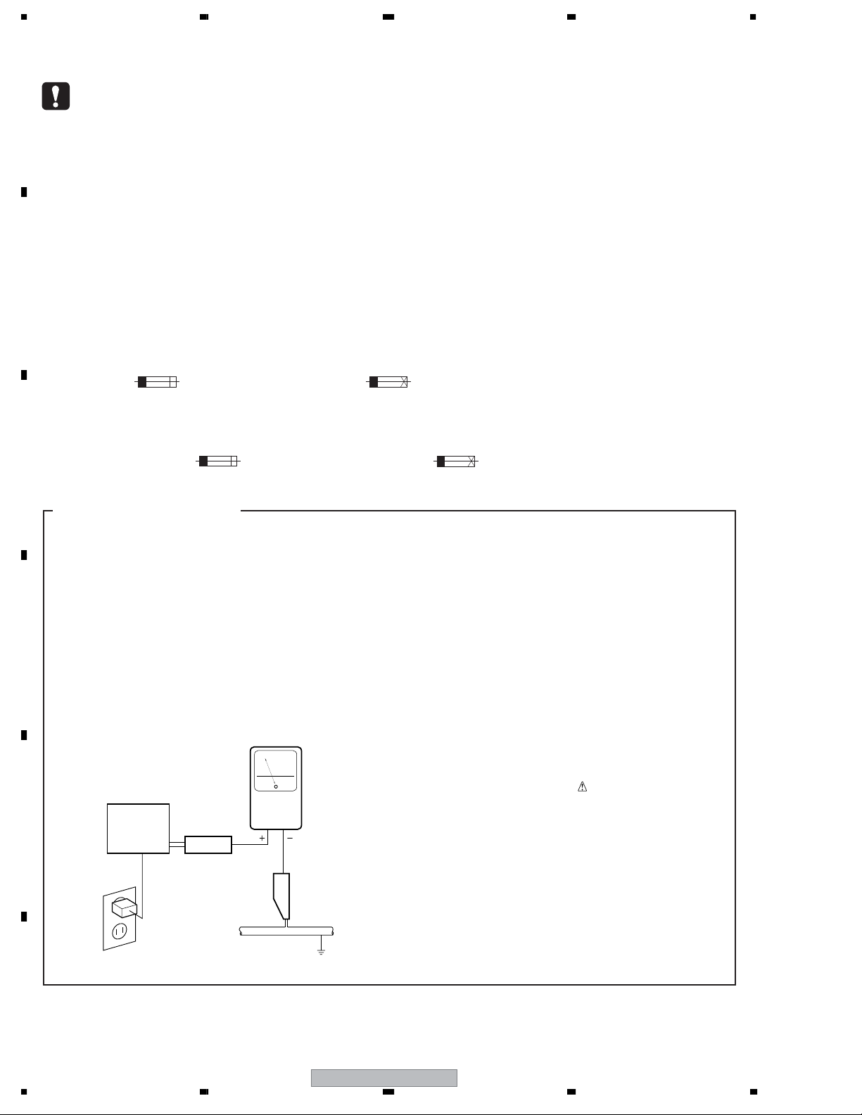
1. SAFETY PRECAUTIONS
The following check should be performed for the
continued protection of the customer and service
technician.
LEAKAGE CURRENT CHECK
Measure leakage current to a known earth ground
(water pipe, conduit, etc.) by connecting a leakage
current tester such as Simpson Model 229-2 or
D
equivalent between the earth ground and all exposed
metal parts of the appliance (input/output terminals,
screwheads, metal overlays, control shaft, etc.). Plug
the AC line cord of the appliance directly into a 120V
AC 60 Hz outlet and turn the AC power switch on. Any
current measured must not exceed 0.5 mA.
Leakage
current
E
Device
under
test
Also test with
plug reversed
(Using AC adapter
plug as required)
Test all
exposed metal
surfaces
AC Leakage Test
tester
Reading should
not be above
0.5 mA
Earth
ground
ANY MEASUREMENTS NOT WITHIN THE
LIMITS OUTLINED ABOVE ARE INDICATIVE
OF A POTENTIAL SHOCK HAZARD AND
MUST BE CORRECTED BEFORE RETURNING THE APPLIANCE TO THE CUSTOMER.
2. PRODUCT SAFETY NOTICE
Many electrical and mechanical parts in the appliance
have special safety related characteristics. These are
often not evident from visual inspection nor the
protection afforded by them necessarily can be obtained
by using replacement components rated for voltage,
wattage, etc. Replacement parts which have these
special safety characteristics are identified in this
Service Manual.
Electrical components having such features are
identified by marking with a
on the parts list in this Service Manual.
The use of a substitute replacement component which
does not have the same safety characteristics as the
PIONEER recommended replacement one, shown in the
parts list in this Service Manual, may create shock, fire,
or other hazards.
Product Safety is continuously under review and new
instructions are issued from time to time. For the latest
information, always consult the current PIONEER
Service Manual. A subscription to, or additional copies
of, PIONEER Service Manual may be obtained at a
nominal charge from PIONEER.
on the schematics and
F
2
1234
PDK-50HW3
Page 3
5678
[Important Check Points for Good Servicing]
In this manual, procedures that must be performed during repairs are marked with the below symbol.
Please be sure to confirm and follow these procedures.
1. Product safety
Please conform to product regulations (such as safety and radiation regulations), and maintain a safe servicing environment by
following the safety instructions described in this manual.
1 Use specified parts for repair.
Use genuine parts. Be sure to use important parts for safety.
2 Do not perform modifications without proper instructions.
Please follow the specified safety methods when modification(addition/change of parts) is required due to interferences such as
radio/TV interference and foreign noise.
3 Make sure the soldering of repaired locations is properly performed.
When you solder while repairing, please be sure that there are no cold solder and other debris.
Soldering should be finished with the proper quantity. (Refer to the example)
4 Make sure the screws are tightly fastened.
Please be sure that all screws are fastened, and that there are no loose screws.
5 Make sure each connectors are correctly inserted.
Please be sure that all connectors are inserted, and that there are no imperfect insertion.
6 Make sure the wiring cables are set to their original state.
Please replace the wiring and cables to the original state after repairs.
In addition, be sure that there are no pinched wires, etc.
7 Make sure screws and soldering scraps do not remain inside the product.
Please check that neither solder debris nor screws remain inside the product.
8 There should be no semi-broken wires, scratches, melting, etc. on the coating of the power cord.
Damaged power cords may lead to fire accidents, so please be sure that there are no damages.
If you find a damaged power cord, please exchange it with a suitable one.
9 There should be no spark traces or similar marks on the power plug.
When spark traces or similar marks are found on the power supply plug, please check the connection and advise on secure
connections and suitable usage. Please exchange the power cord if necessary.
0 Safe environment should be secured during servicing.
When you perform repairs, please pay attention to static electricity, furniture, household articles, etc. in order to prevent injuries.
Please pay attention to your surroundings and repair safely.
A
B
C
D
2. Adjustments
To keep the original performance of the products, optimum adjustments and confirmation of characteristics within specification.
Adjustments should be performed in accordance with the procedures/instructions described in this manual.
3. Lubricants, Glues, and Replacement parts
Use grease and adhesives that are equal to the specified substance.
Make sure the proper amount is applied.
4. Cleaning
For parts that require cleaning, such as optical pickups, tape deck heads, lenses and mirrors used in projection monitors, proper
cleaning should be performed to restore their performances.
5. Shipping mode and Shipping screws
To protect products from damages or failures during transit, the shipping mode should be set or the shipping screws should be
installed before shipment. Please be sure to follow this method especially if it is specified in this manual.
56
PDK-50HW3
E
F
3
7
8
Page 4

1234
CONTENTS
SAFETY INFORMATION..................................................................................................................................... 2
1. SPECIFICATIONS ............................................................................................................................................ 5
2. EXPLODED VIEWS AND PARTS LIST ............................................................................................................ 6
A
B
C
D
E
2.1 PACKING ................................................................................................................................................... 6
2.2 EXTERIOR................................................................................................................................................. 8
2.3 PEN.......................................................................................................................................................... 10
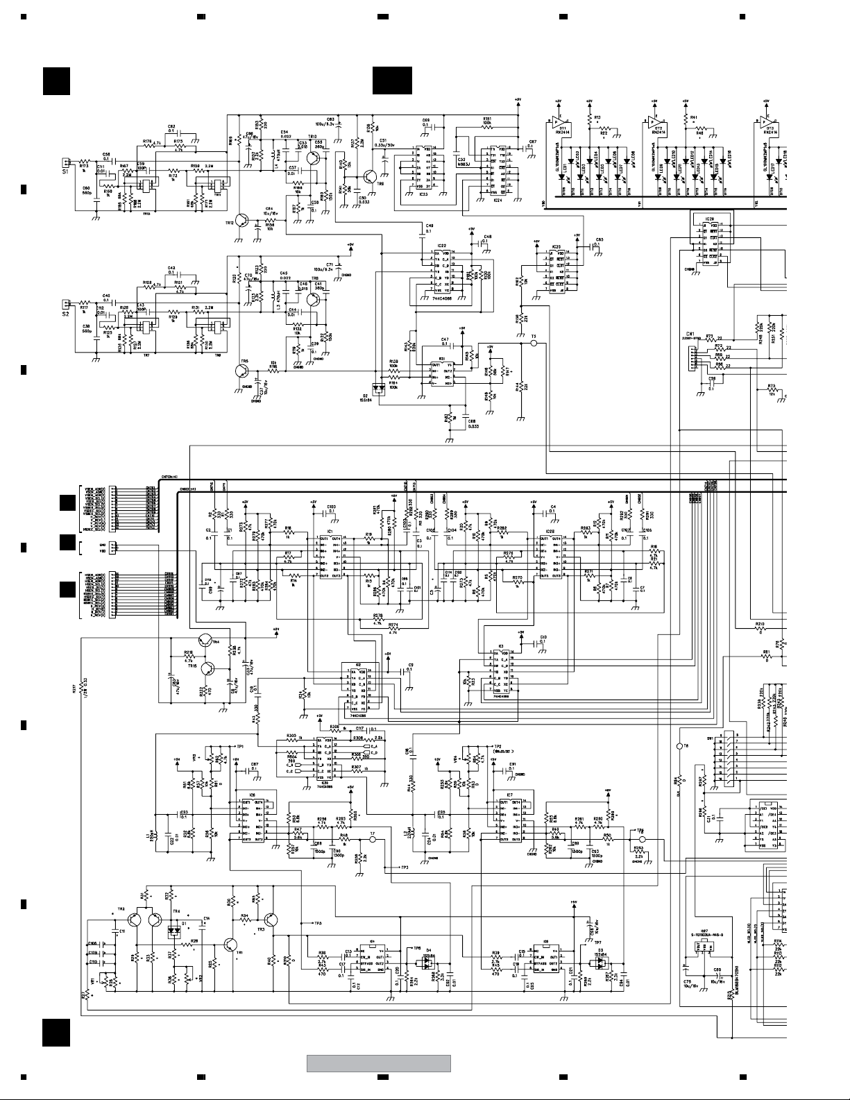
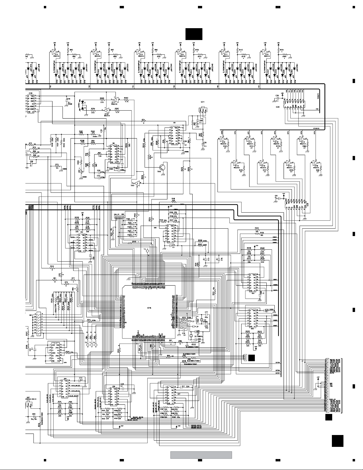
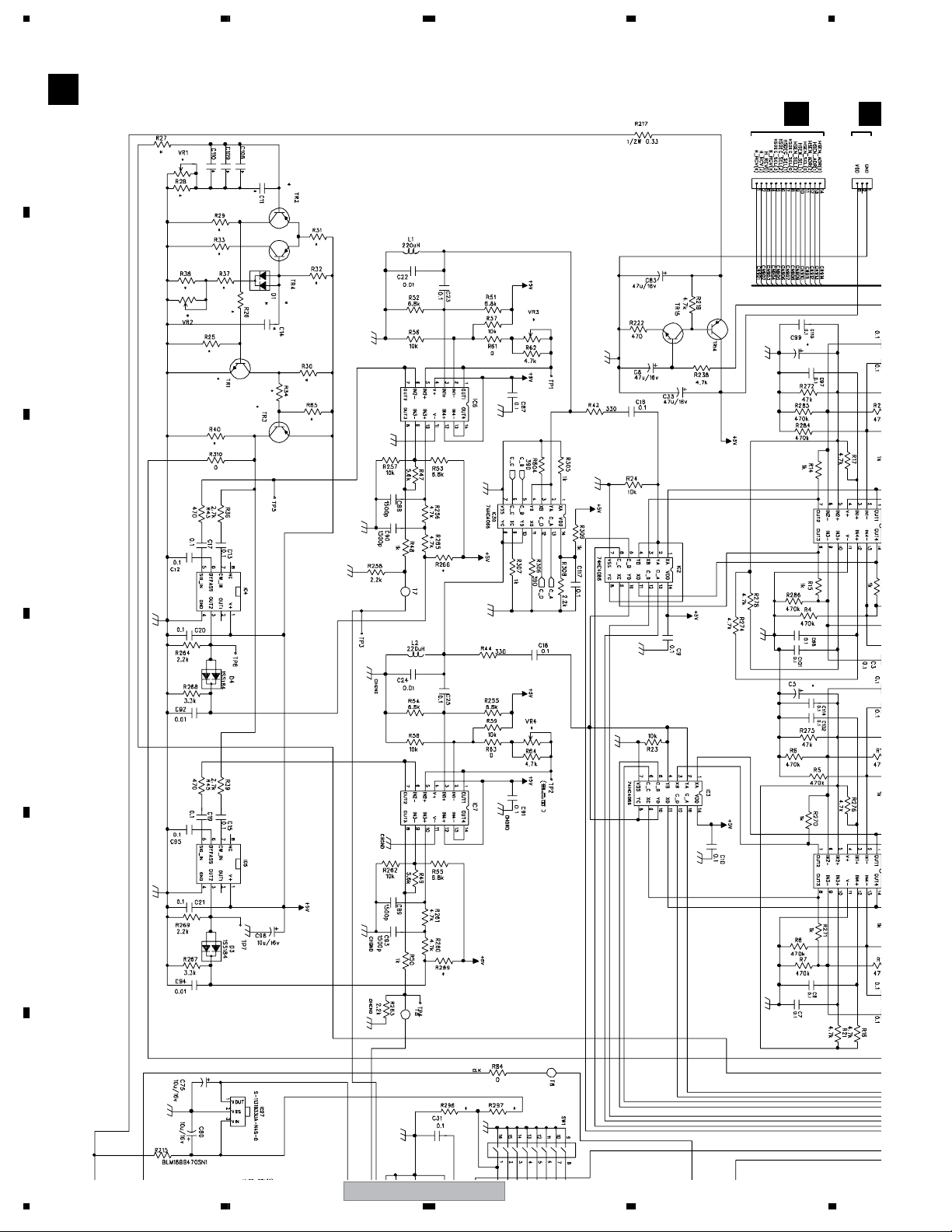
3. BLOCK DIAGRAM AND SCHEMATIC DIAGRAM..........................................................................................12
3.1 BLOCK DIAGRAM ................................................................................................................................... 12
3.1.1 OVERALL BLOCK DIAGRAM ........................................................................................................... 12
3.1.2 LED AND SENSOR BLOCK DIAGRAM............................................................................................ 14
3.2 OVERALL WIRING DIAGRAM................................................................................................................. 16
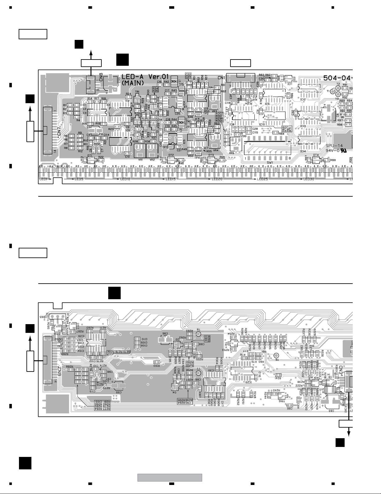
3.3 LED-A ASSY (GUIDE PAGE)................................................................................................................... 18
3.4 LED-A ASSY............................................................................................................................................ 20
3.5 LED-B ASSY............................................................................................................................................ 24
3.6 LED-C ASSY............................................................................................................................................ 26
3.7 LED-D ASSY............................................................................................................................................ 28
3.8 LED-E ASSY............................................................................................................................................ 30
3.9 LED-F ASSY ............................................................................................................................................ 32
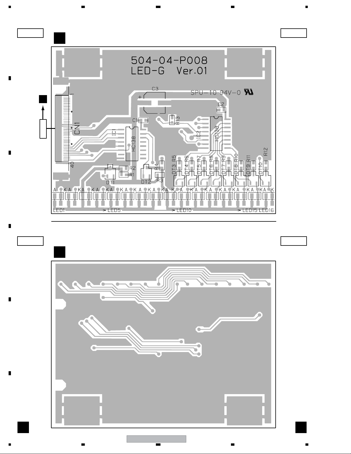
3.10 LED-G ASSY ......................................................................................................................................... 34
3.11 SENSOR-H ASSY ................................................................................................................................. 36
3.12 SENSOR-I ASSY ................................................................................................................................... 38
3.13 SENSOR-J ASSY ..................................................................................................................................40
3.14 SENSOR-K ASSY.................................................................................................................................. 42
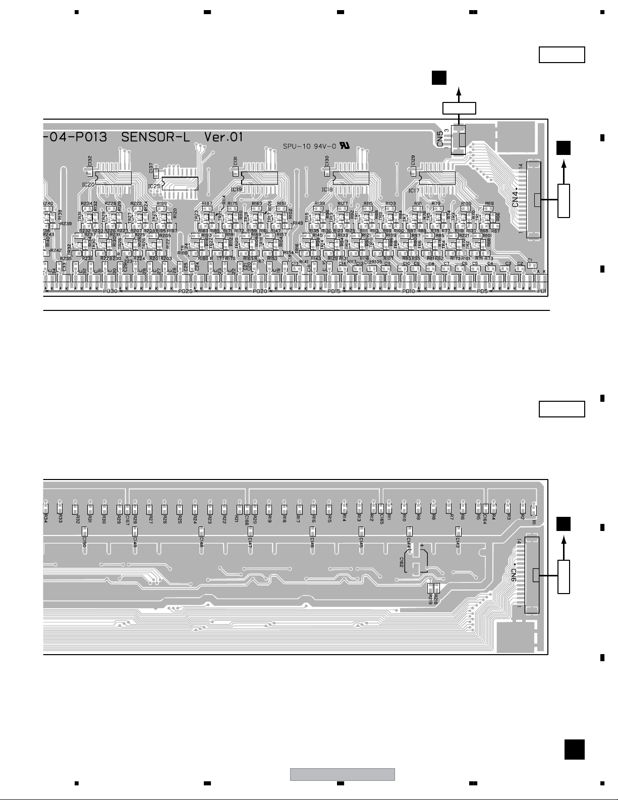
3.15 SENSOR-L ASSY .................................................................................................................................. 44
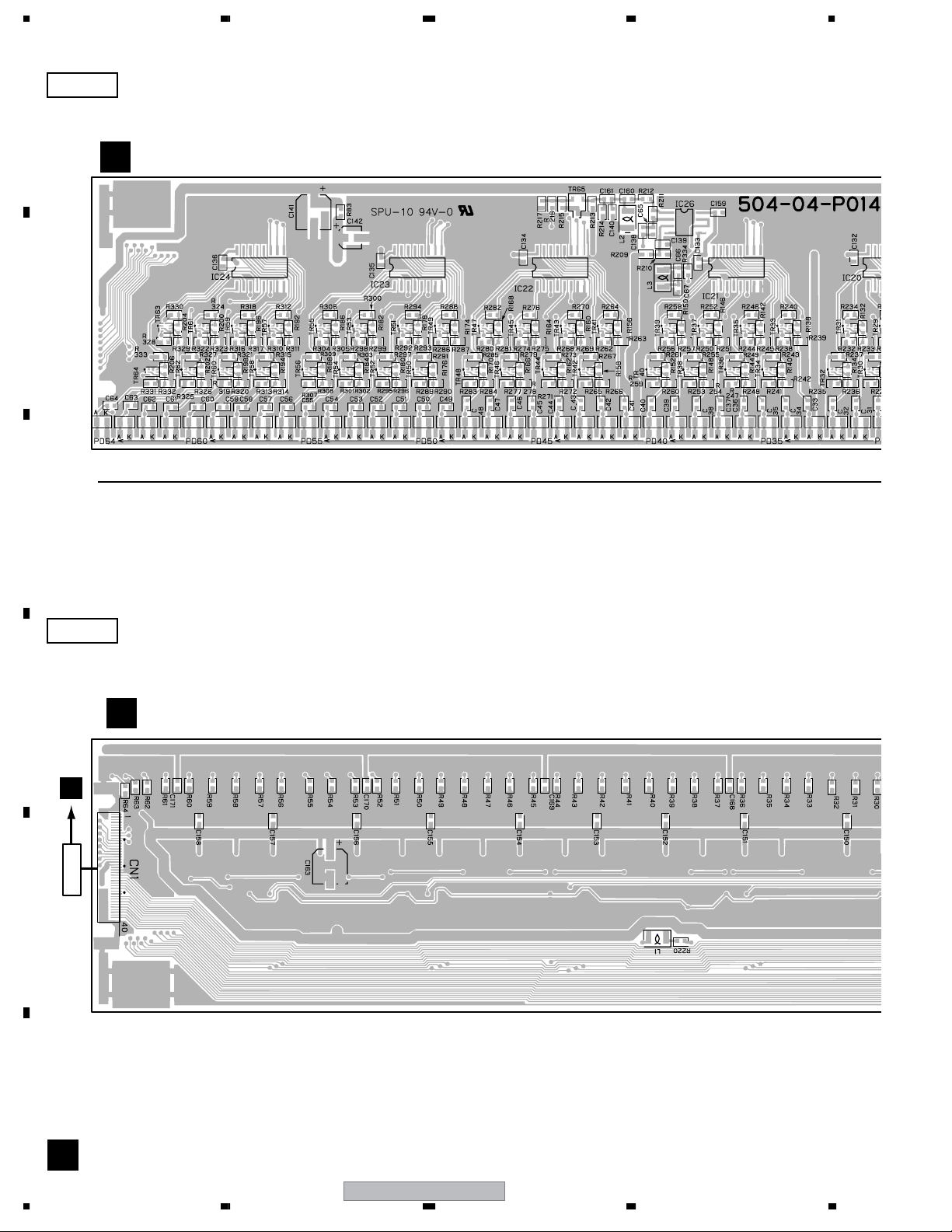
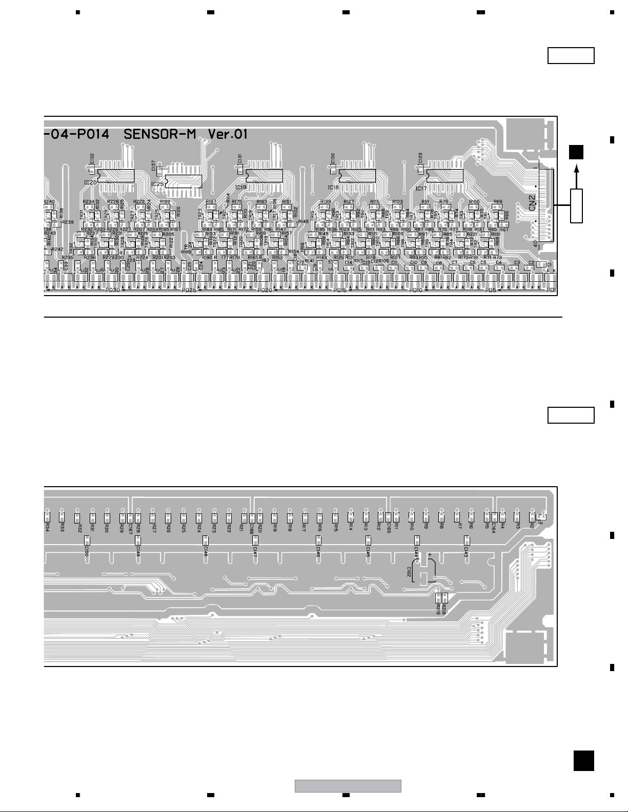
3.16 SENSOR-M ASSY ................................................................................................................................. 46
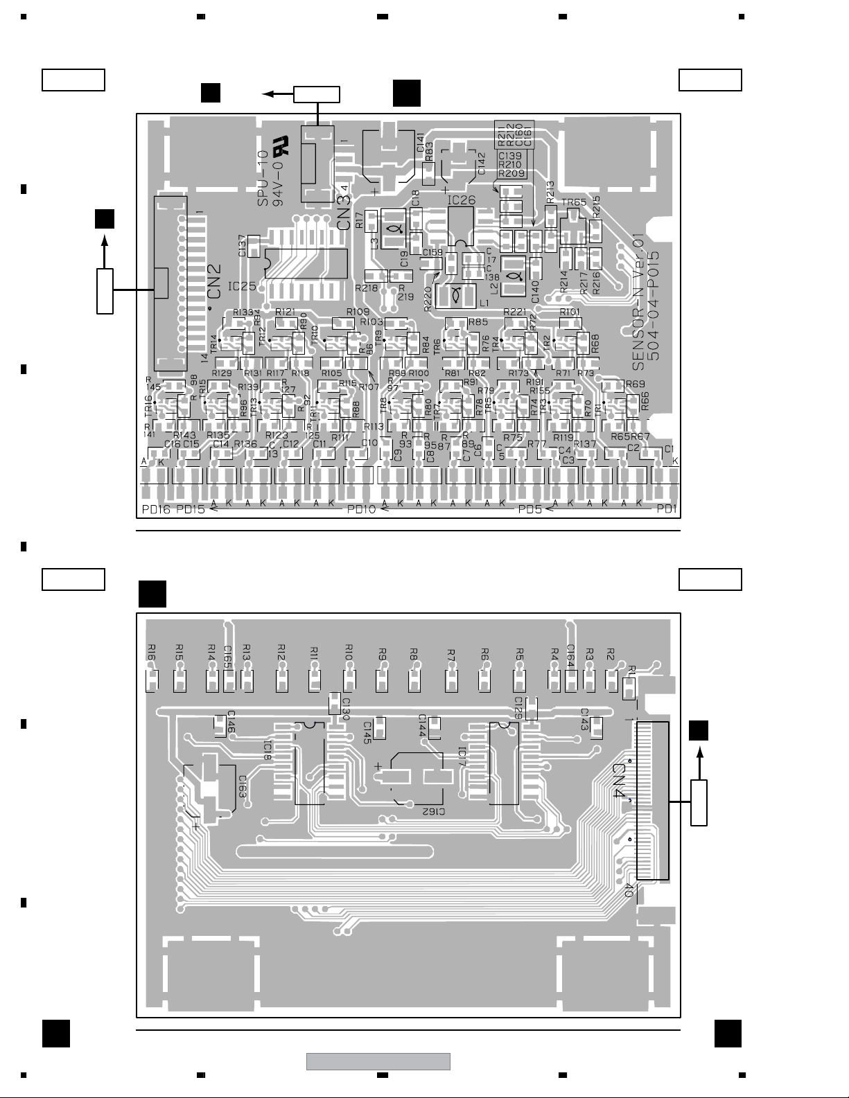
3.17 SENSOR-N ASSY ................................................................................................................................. 48
3.18 USB BOARD ASSY ...............................................................................................................................49
3.19 PEN PCB ASSY..................................................................................................................................... 50
3.20 WAVEFORMS ........................................................................................................................................ 52
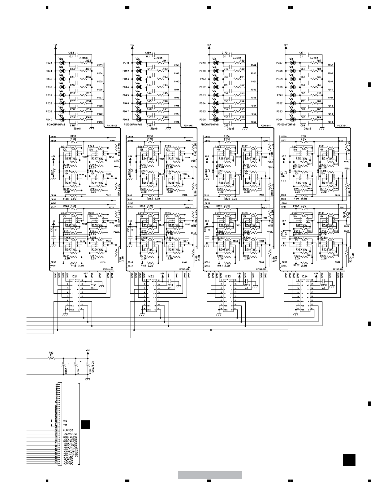
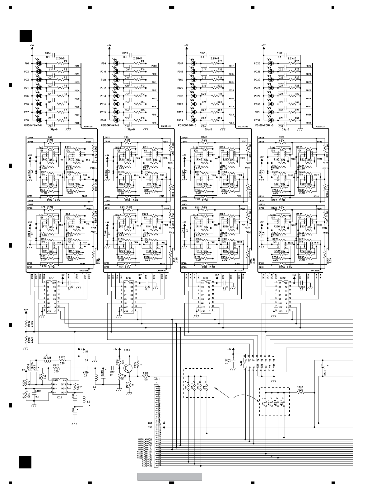
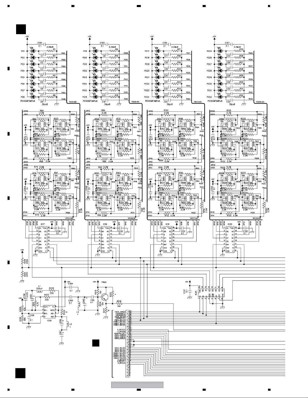
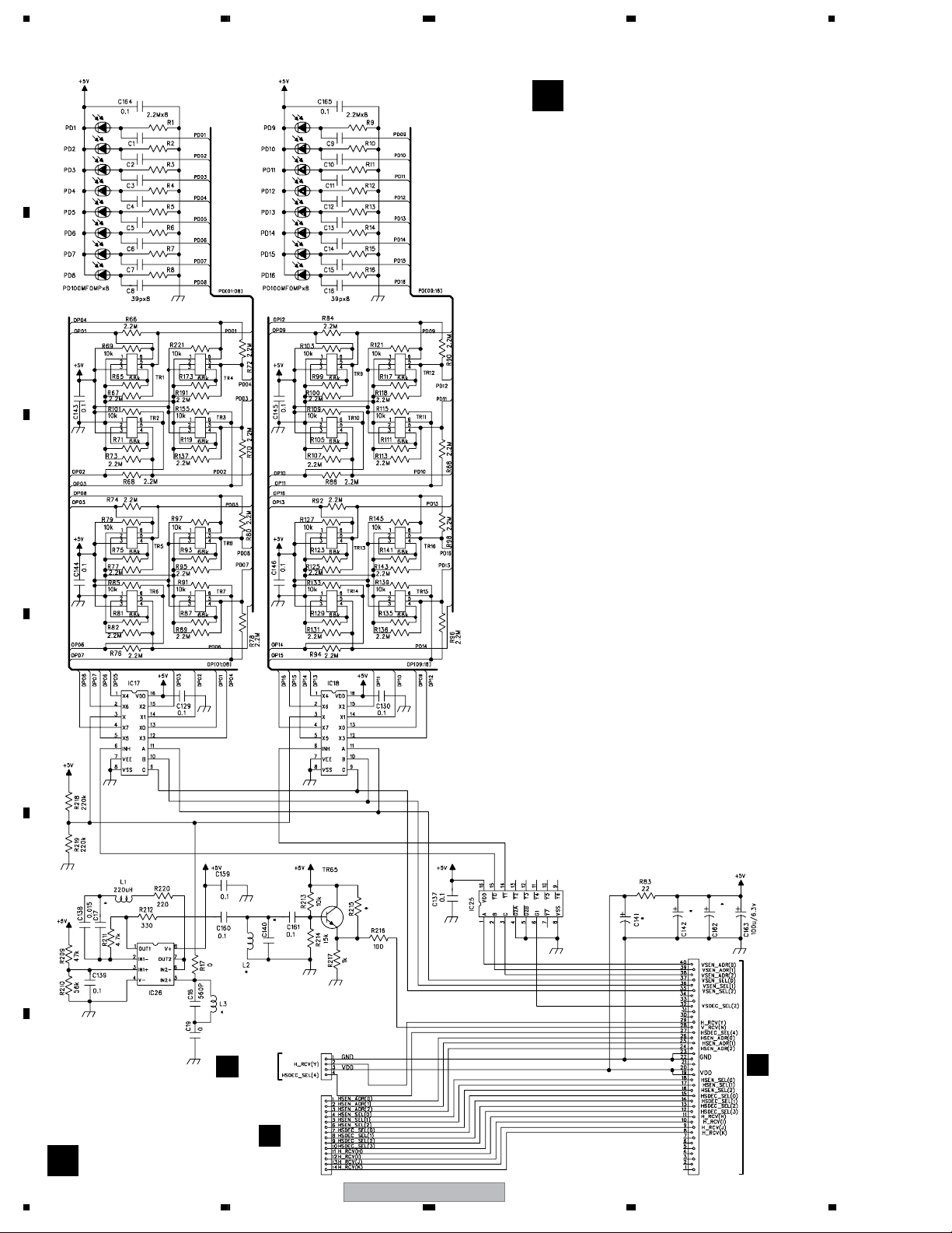
4. PCB CONNECTION DIAGRAM ..................................................................................................................... 53
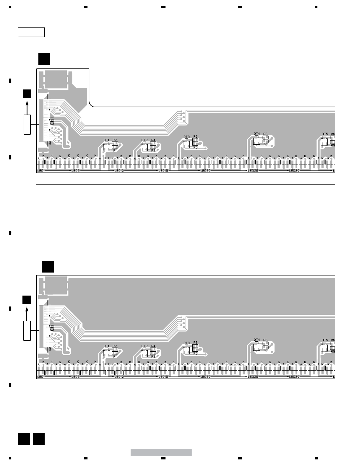
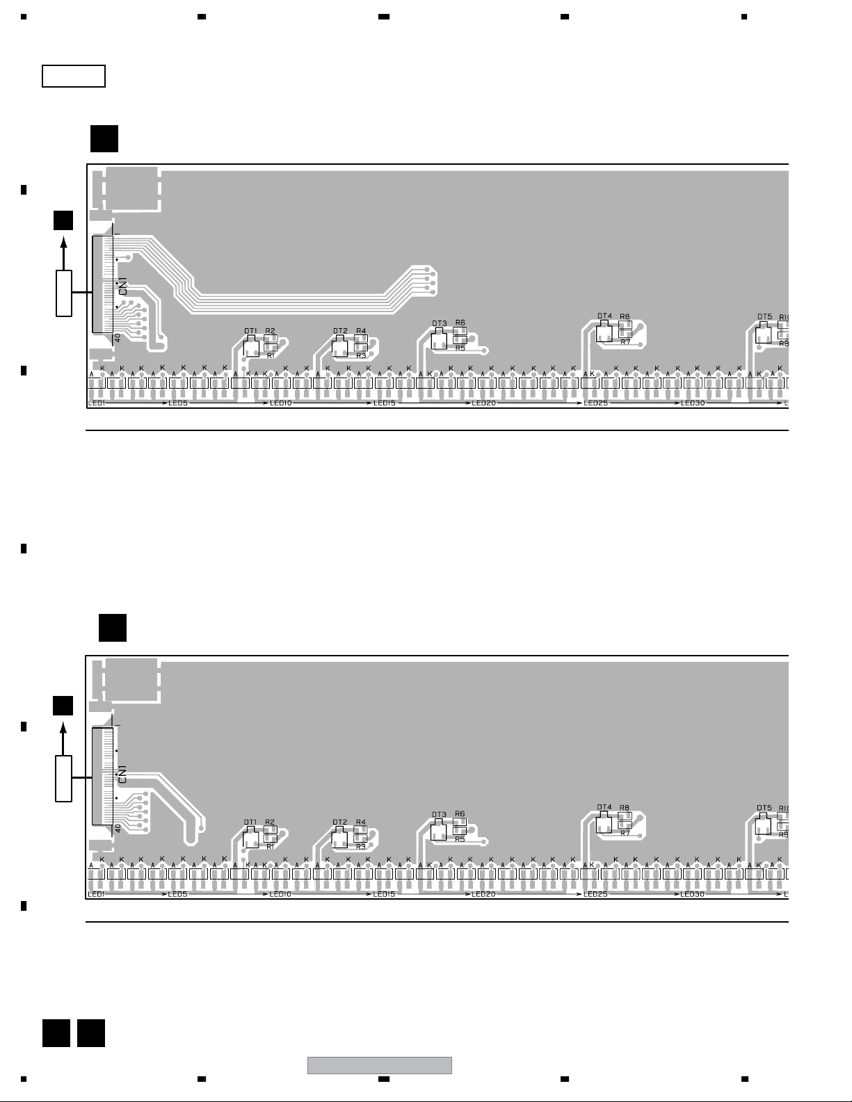
4.1 LED-A ASSY............................................................................................................................................ 54
4.2 LED-B and LED-C ASSYS....................................................................................................................... 56
4.3 LED-D and LED-F ASSYS....................................................................................................................... 58
4.4 LED-E ASSY............................................................................................................................................ 60
4.5 LED-G ASSY ........................................................................................................................................... 62
4.6 SENSOR-H ASSY ................................................................................................................................... 64
4.7 SENSOR-I ASSY ..................................................................................................................................... 66
4.8 SENSOR-J ASSY ....................................................................................................................................68
4.9 SENSOR-K ASSY.................................................................................................................................... 70
4.10 SENSOR-L ASSY .................................................................................................................................. 72
4.11 SENSOR-M ASSY ................................................................................................................................. 74
4.12 SENSOR-N ASSY ................................................................................................................................. 76
4.13 USB BOARD ASSY ...............................................................................................................................77
4.14 PEN PCB ASSY..................................................................................................................................... 78
5. PCB PARTS LIST ........................................................................................................................................... 79
6. ADJUSTMENT ............................................................................................................................................... 86
7. GENERAL INFORMATION............................................................................................................................. 87
7.1 DIAGNOSIS ............................................................................................................................................. 87
7.1.1 TEST MODE ...................................................................................................................................... 87
7.1.2 SELF TEST FUNCTION (SelfTest) .................................................................................................... 88
7.1.3 INTERNAL DIP SWITCH SETTINGS................................................................................................ 90
7.1.4 OPERATION CHECKS USING EXCHANGEABLE ASSY'S ............................................................. 91
8. PANEL FACILITIES ........................................................................................................................................ 92
F
4
1234
PDK-50HW3
Page 5
5678
1. SPECIFICATIONS
Scanning system...........................................................................................Infrared scanning
Power indicator..................................................................................................................LED
Interface......................................................................................................................USB 1.1
Power supply..............................................................................Bus-powered from USB port
Power consumption........................................................................................Maximum 2.5W
External dimensions
(including plasma display, excluding pen stand).................1,258 (W) x 758 (H) x 115 (D) mm
Weight (excluding plasma display, including pen stand[0.6 kg]).....................................7.4 kg
Dedicated Pen
Transmission...................................................................................................Ultrasonic wave
Operation switches...............................................................................Pen tip (x1), Body (x2)
Power......................................................................................AAA (LR03) alkaline battery x 1
External dimensions..............................................................................18.5 (W) x 186 (L) mm
Weight (including battery).................................................................................................43 g
Accessories
Pen........................................................................................................................................1
AAA (LR03) alkaline batteries..................................................................................................................2
Replacement pen tips............................................................................................................2
Allen bolt................................................................................................................................1
Pen stand...............................................................................................................................1
Operating Instructions............................................................................................................1
CD-ROM(Driver software disc)..............................................................................................1
Driver Installation Guide.........................................................................................................1
¶ Specifications and appearance may change without notice.
Dimensional Diagram
(View when this unit installed on the PDP-504CMX/PDP-50MXE1)
1258
(excluding the bolt head)
74
115
92
A
B
C
Unit: mm
• Accessories
Pen (x1)
(BZX1287)
AAA (LR03)
alkaline batteries (x2)
Replacement tips (x2)
(BZE2027)
758
120220
Allen bolt (x1)
(SMZ80H200FNI)
Pen stand (x1)
(BZN2398)
Operating Instructions (x1)
CD-ROM(Driver software disc) (x1)
Driver Installation Guide (x1)
D
58
56
E
F
56
PDK-50HW3
5
7
8
Page 6
1234
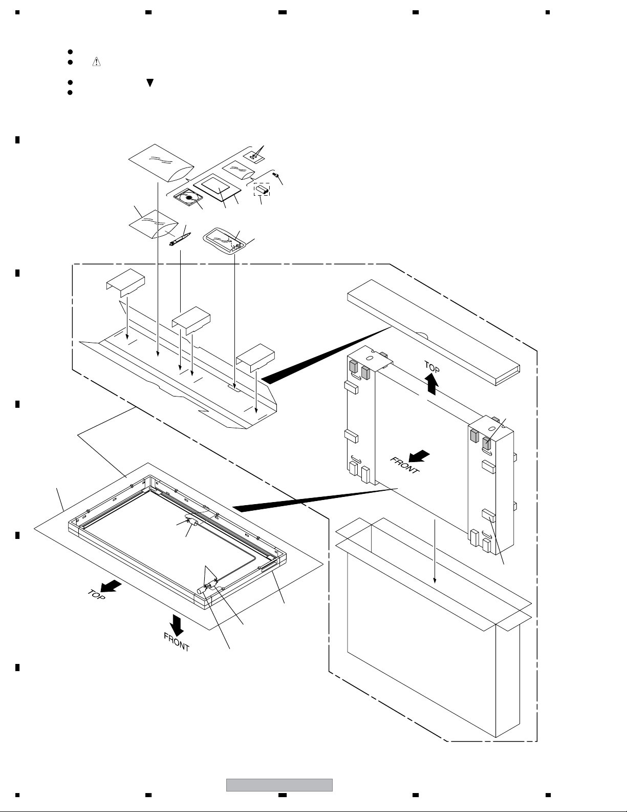
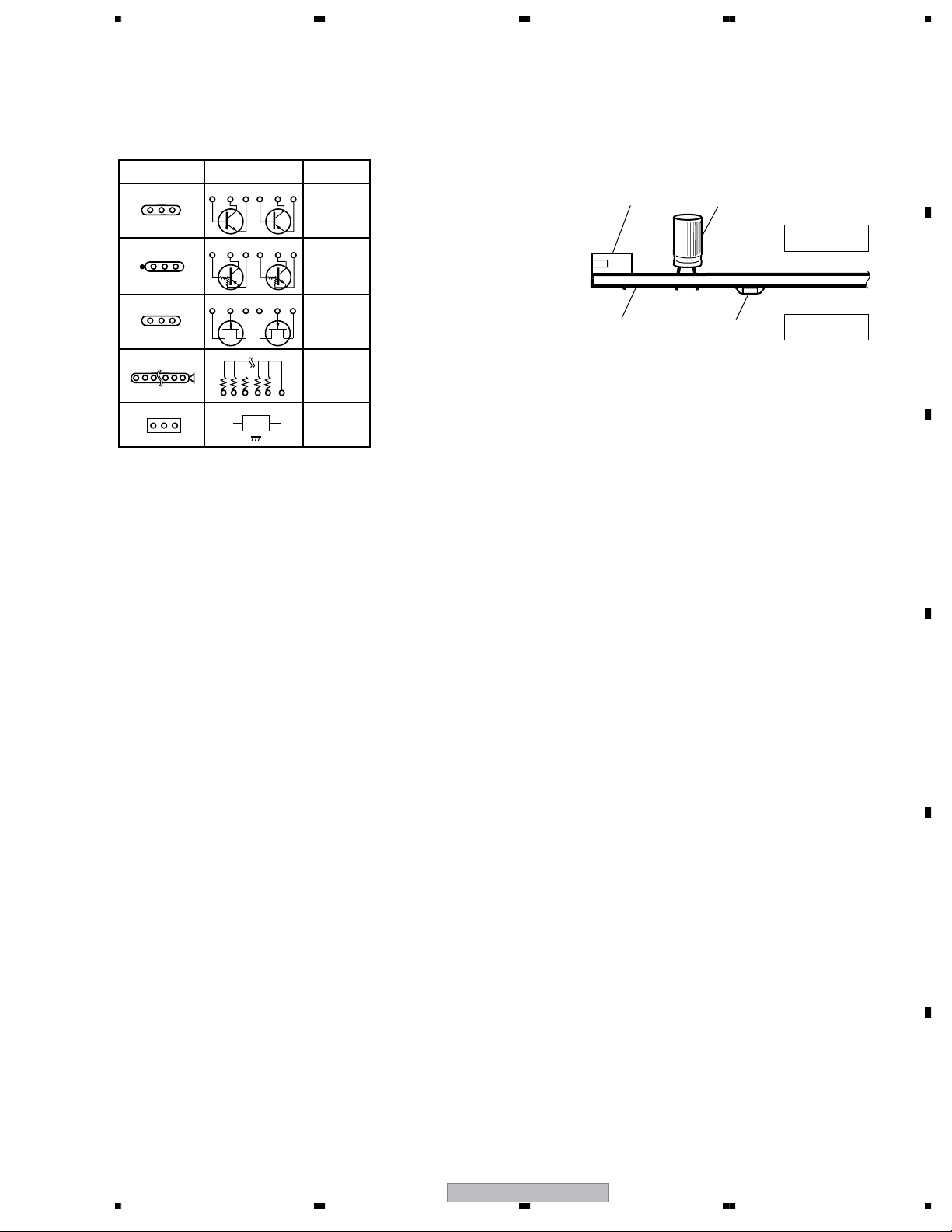
2. EXPLODED VIEWS AND PARTS LIST
NOTES:
Parts marked by "NSP" are generally unavailable because they are not in our Master Spare Parts List.
The mark found on some component parts indicates the importance of the safety factor of the part.
A
Therefore, when replacing, be sure to use parts of identical designation.
Screws adjacent to mark on product are used for disassembly.
For the applying amount of lubricants or glue, follow the instructions in this manual.
(In the case of no amount instructions, apply as you think it appropriate.)
2.1 PACKING
Air Cap Bag 1 (200 x 75)
B
C
3
4
6
7
1
8
2
5
Mirror Mat (350 x 550)
D
Mirror Mat
(1400 x 1800)
E
Pink
Pad
9
vinyl tie
Air Cap Sheet
(150 x 100)
vinyl tie
White
Pad
PDK-50HW3
Air Cap Sheet
(150 x 100)
Air Cap Bag 2
(75 x 100)
F
6
1234
PDK-50HW3
Page 7
5678
PACKING SECTION PARTS LIST
No. Description Part No.
No. Description Part No.
Mark
1Pen BZX1287
2 AAA (LR03) alkaline batteries • • • • •
3 Replacement Tips BZE2027
4 Allen Bolt SMZ80H200FNI
5Pen Stand BZN2398
Mark
6 Operating Instructions See Contrast table (2)
7 CD-ROM (Driver software disc) BZR1372
8Driver Installation Guide BZR1373
9Packing Set See Contrast table (2)
10 Label See Contrast table (2)
(2) CONTRAST TABLE
PDK-50HW3/UCYVBKE and Z/CN types are constructed the same except for the following:
A
Mark No. Description
6 Operating Instructions
(Japanese, English, French, German,
Italian, Dutch, Spanish, Chinese, Korean)
6 Operating Instructions Not used BZR1374
9Packing Set BZH1557 BZH1558
10 Label BZR1383 Not used
PDK-50HW3
/UCYVBKE
BZR1370 Not used
PDK-50HW3
/Z/CN
B
C
D
56
PDK-50HW3
E
F
7
7
8
Page 8

1234
2.2 EXTERIOR
45
14
44
45
45
42
45
36
42
39
45
47
41
35
17
25
39
41
41
51
16
36
45
1
15
37
A
30
13
32
12
45
36
46
L
O
M
B
C
46
N
46
2
45
44
42
41
42
16
34
3
4
45
D
A
47
42
B
26
C
41
41
29
45
24
5
6
39
45
44
42
47
42
H
46
I
8
D
39
E
33
41
45
42
9
10
45
44
42
47
42
41
52
16
J
K
G
11
29
45
42
E
F
45
30
7
31
36
28
16
40
F
8
27
PDK-50HW3
1234
Page 9
5678
Wiring Diagram
14
18
N
21
22
18
A
1
19
15
43
A
O
49
50
48
38
B
2
D
4
18
20
23
B
12
21
L
H
8
E
5
EXTERIOR SECTION PARTS LIST
No. Description Part No.
Mark
1 LED-A Assy BZW1509
2 LED-B Assy BZW1510
3 LED-C Assy BZW1511
4 LED-D Assy BZW1512
5 LED-E Assy BZW1513
6 LED-F Assy BZW1514
7 LED-G Assy BZW1515
8 SENSOR-H Assy BZW1516
9 SENSOR-I Assy BZW1517
10 SENSOR-J Assy BZW1518
11 SENSOR-K Assy BZW1519
12 SENSOR-L Assy BZW1520
13 SENSOR-M Assy BZW1521
14 SENSOR-N Assy BZW1522
15 USB BOARD Assy BZW1523
16 Sensor Holder AZN2425
17 Filter LED AZN2429
18 3P Connector Assy BZD1402
19 4P Connector Assy BZD1403
20 10P Connector Assy BZD1404
21 14P Connector Assy BZD1405
22 14P Connector Assy (Red) BZD1406
23 USB Cable BZD1411
24 Escutcheon BZN2376
25 Corner (Left Lower) BZN2377
26 Corner (Left Upper) BZN2379
27 Corner (Right Upper) BZN2380
No. Description Part No.
Mark
28 Filter RC BZN2381
29 Filter UL BZN2382
30 Filter LR BZN2383
31 Frame (Right) BZN2385
32 Frame (Left) BZN2386
33 Frame (Upper) BZN2388
34 Frame (Lower) BZN2389
35 Indicator Window BZN2399
36 Hook BZN2400
37 USB Cable Clamp BZN2401
38 Spacer BZN2403
39 Locking Fixture Assy BZN2404
40 Corner (Right Lower) BZN2406
41 Screw BZB1476
42 Screw BZB1477
43 Screw BZB1478
44 Screw BPZ30P080FTC
45 Screw PMB40P080FTB
NSP 46 Screw PMA30P060FTC
NSP 47 Screw PMA30P040FTC
NSP 48 Washer WC30FTC
NSP 49 Washer WS30FTC
NSP 50 Nut NA30FTC
51 SS Sensor L BZP1025
52 SS sensor R BZP1026
C
D
E
F
56
PDK-50HW3
9
7
8
Page 10
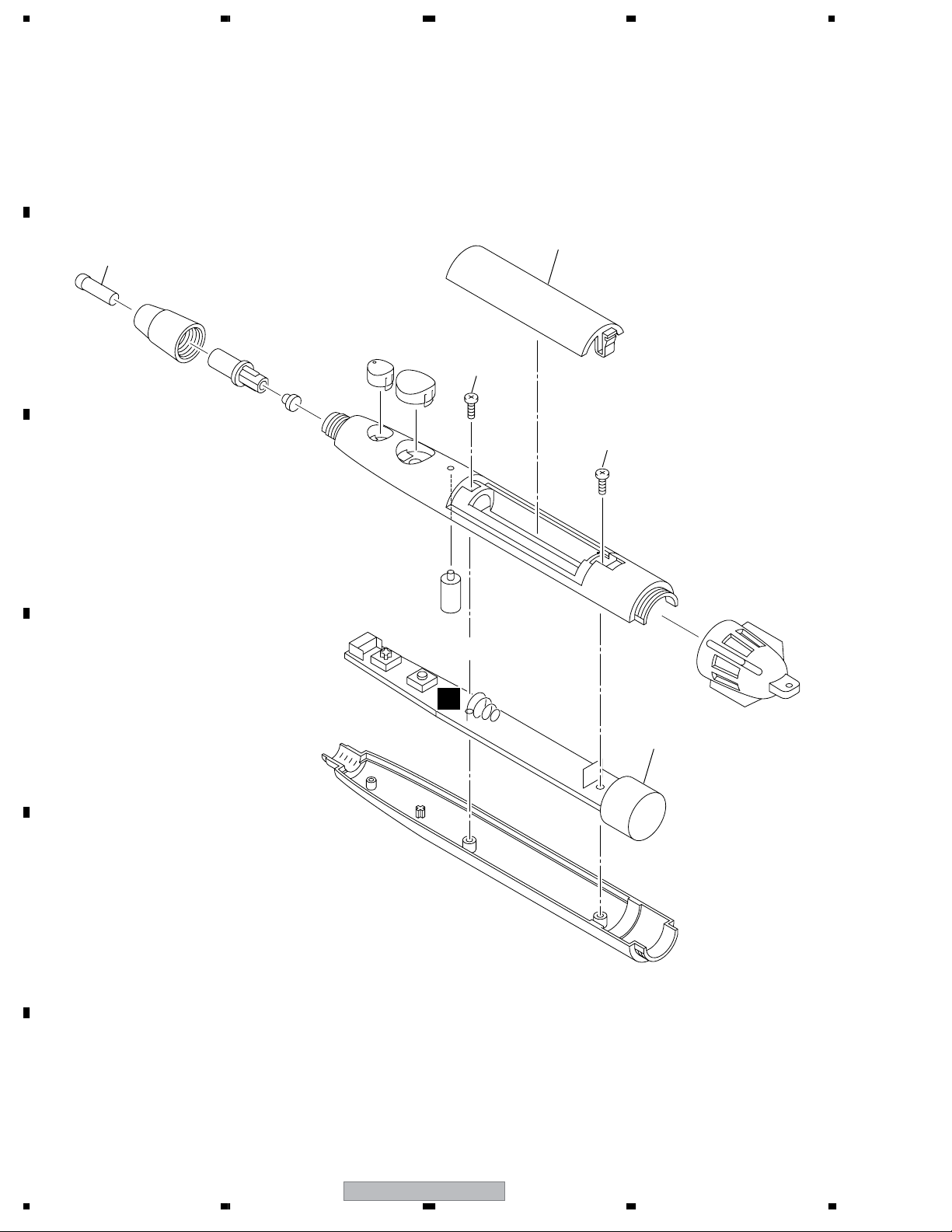
2.3 PEN
A
B
1234
2
3
4
4
C
D
E
P
1
F
10
1234
PDK-50HW3
Page 11

5678
PEN SECTION PARTS LIST
No. Description Part No.
Mark
1 PEN PCB Assy BZW1524
2 Battery Cover BZN2392
3Pen Tip BZE2027
NSP 4 Screw PBZ20P050FTB
A
B
C
D
E
56
PDK-50HW3
F
11
7
8
Page 12
1234
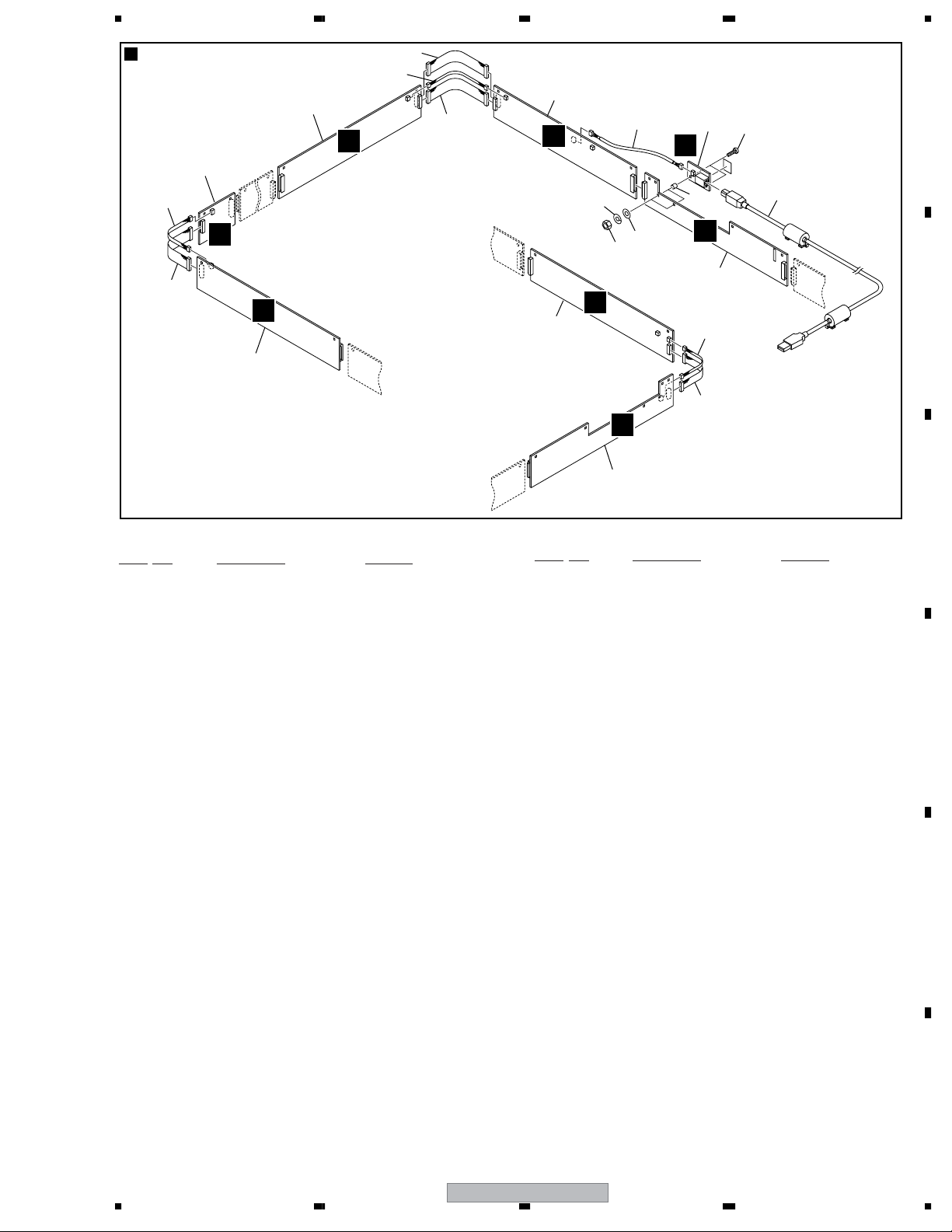
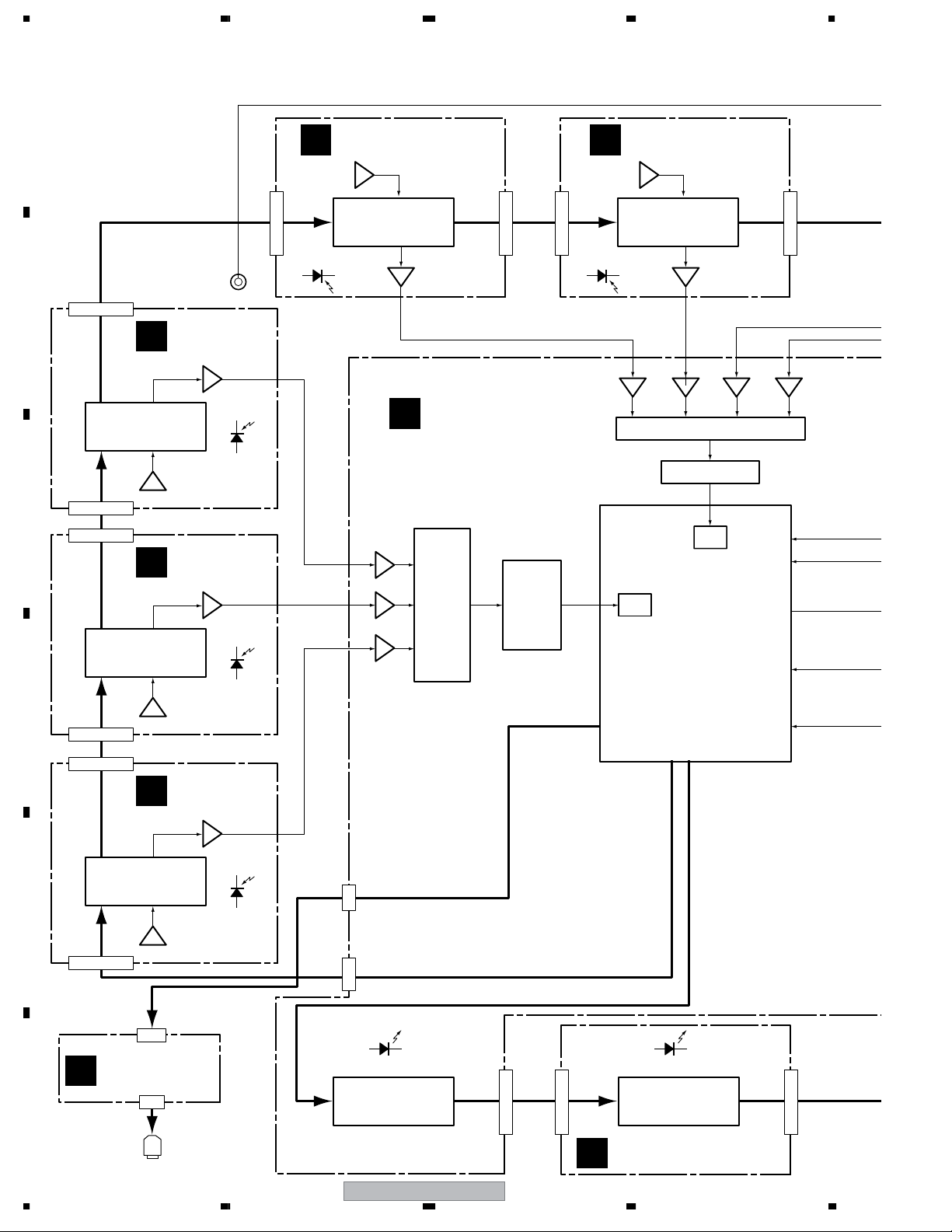
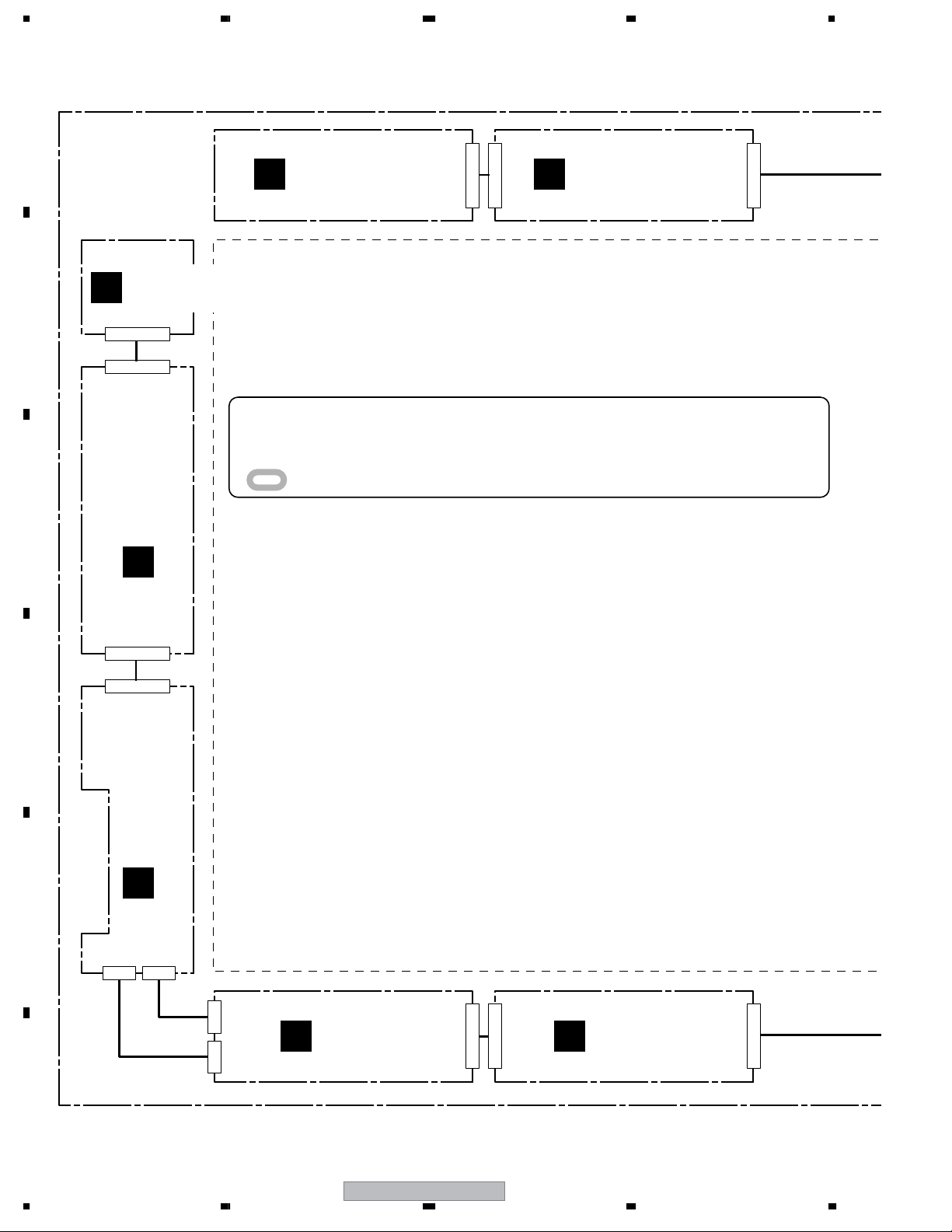
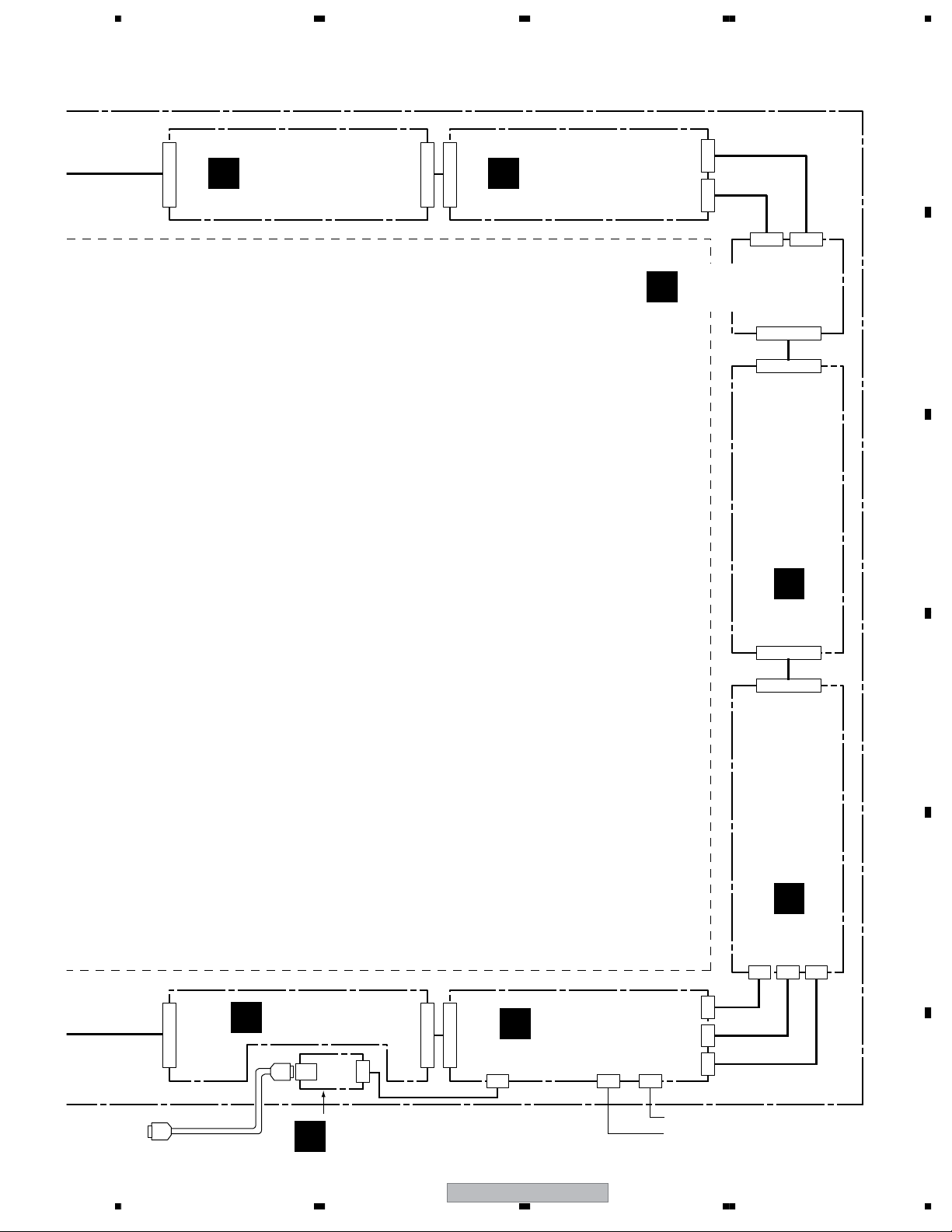
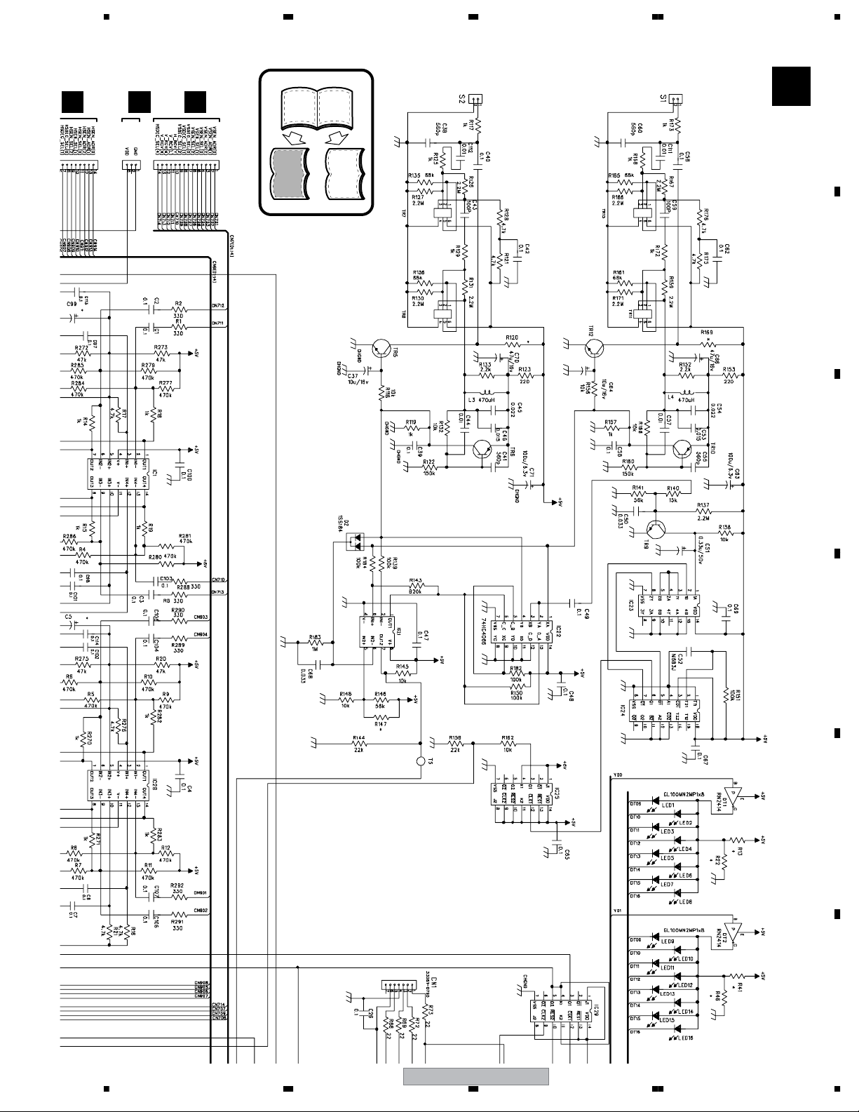
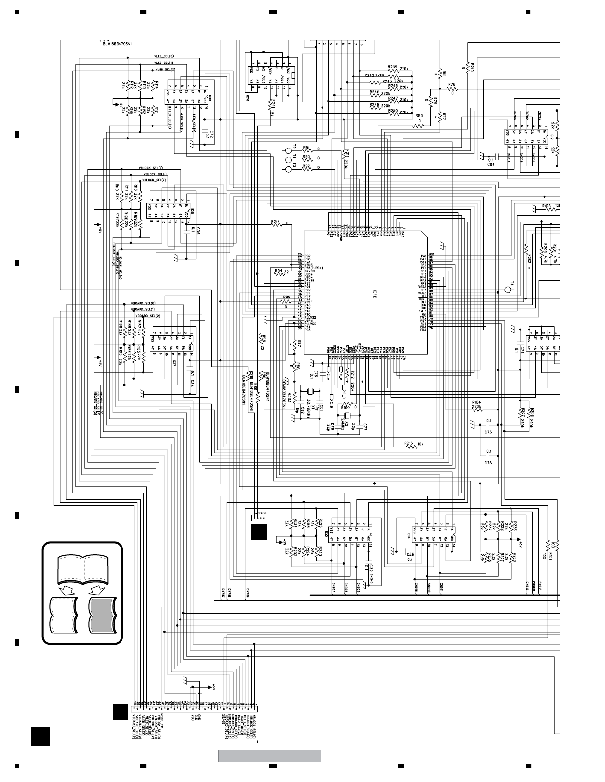
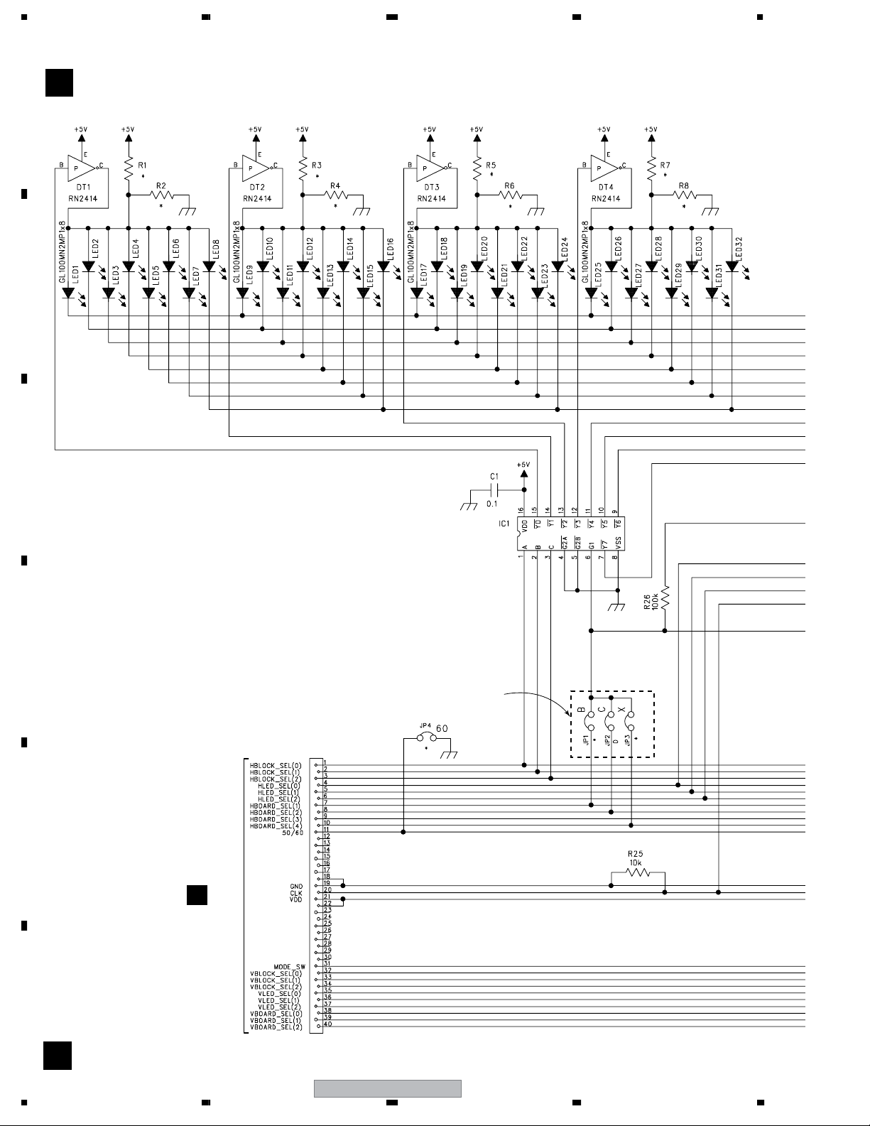
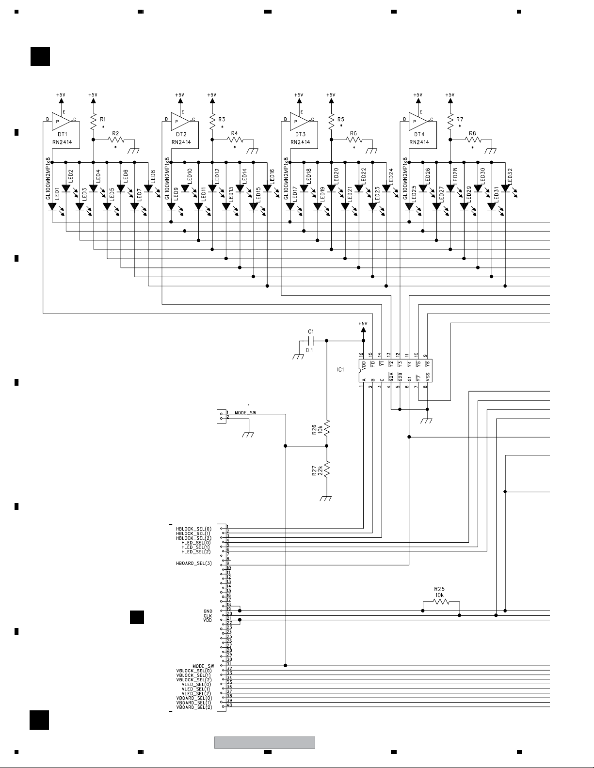
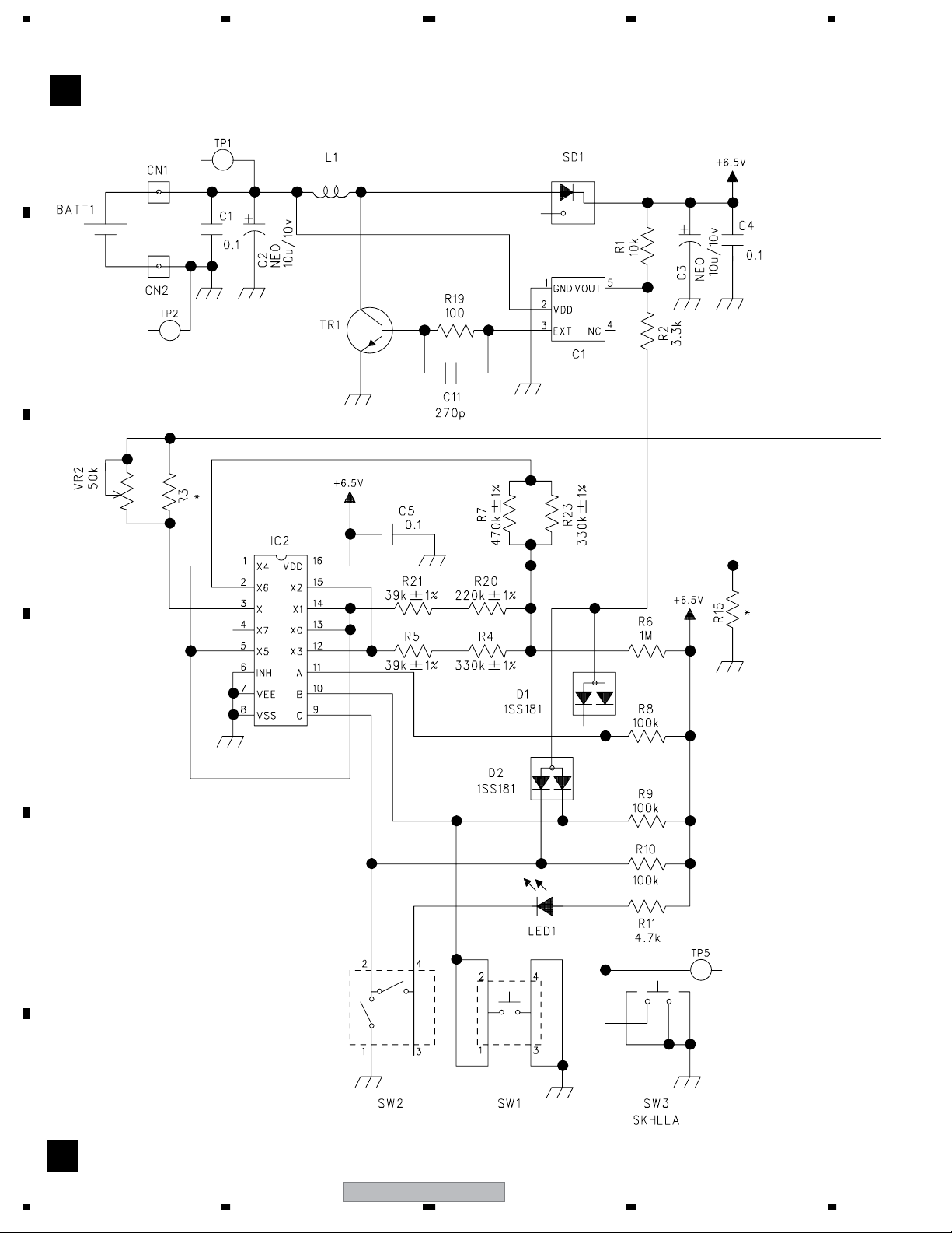
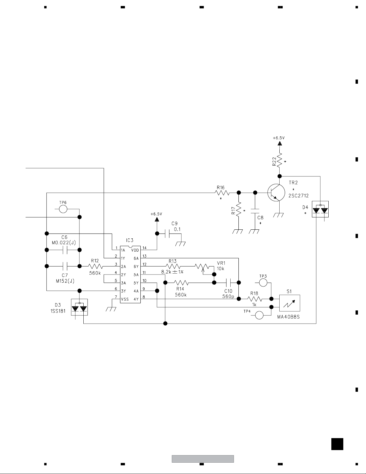
3. BLOCK DIAGRAM AND SCHEMATIC DIAGRAM
3.1 BLOCK DIAGRAM
3.1.1 OVERALL BLOCK DIAGRAM
A
SENSOR-H ASSY
H
Amp
CN5,
CN6
Horizontal decoding,
sensor and address
selector
64 IR sensors
Ultra Sonic MIC
B
CN2,
CN3
Vertical decoding,
sensor and address
selector
CN4
C
CN1
Vertical decoding,
sensor and address
selector
D
CN2
SENSOR-N
N
ASSY
Amp
SENSOR-M
M
ASSY
Amp
Buffer
16 IR
sensors
Buffer
64 IR
sensors
Amp
Amp
Amp
Buffer
LED-A ASSY
A
Vertical
Sensor
Selector
CN1
64 IR sensors
Detection
SENSOR-I ASSY
I
Amp
CN4
Horizontal decoding,
sensor and address
selector
Horizontal Sensor Selector
A/D
MAIN CPU
Buffer
Amp
Detection
A/D
CN1
Amp AmpAmp
CN1
Vertical decoding,
sensor and address
selector
E
CN4CN6
USB BOARD
O
ASSY
F
USB CABLE
12
1234
SENSOR-L
L
ASSY
Amp
CN2
CN1
Buffer
64 IR
sensors
CN3
CN7-CN9
64 IR LEDs
Horizontal Board,
Block and LED
selector
PDK-50HW3
CN4
H & V sens_adr
H & V sens_sel
H & V sdec_sel
CN1
B
64 IR LEDs
Horizontal Board,
Block and LED
selector
LED-B ASSY
H & V block_sel
H & V LED_sel
H & V board_sel
CN4
Page 13

5678
A
SENSOR-J ASSY
J
CN4
Horizontal decoding,
sensor and address
selector
64 IR sensors
POWER indication
DIP switch
Amp
Buffer
CN1
Ultra Sonic
Receiver Amp
Frequency
judgement
SENSOR-K ASSY
K
CN4
Horizontal decoding,
sensor and address
selector
64 IR sensors
Ultra Sonic
Receiver Amp
Amp
Carrier
Buffer
LED-G
G
ASSY
16 IR LEDs
LED-F
F
ASSY
64 IR LEDs
Ultra Sonic MIC
B
Vertical Board,
Block and LED
selector
CN1
C
CN4
Vertical Board,
Block and LED
selector
CN1
C
64 IR LEDs
Horizontal Board,
Block and LED
selector
LED-C ASSY
CN4
CN1
D
56
64 IR LEDs
Horizontal Board,
Block and LED
selector
LED-D ASSY
PDK-50HW3
CN5,CN6
7
LED-E
E
ASSY
64 IR LEDs
PEN/
NORMAL
Vertical Board,
Block and LED
selector
CN2,CN3
CN1
CN4
8
D
E
F
13
Page 14
1234
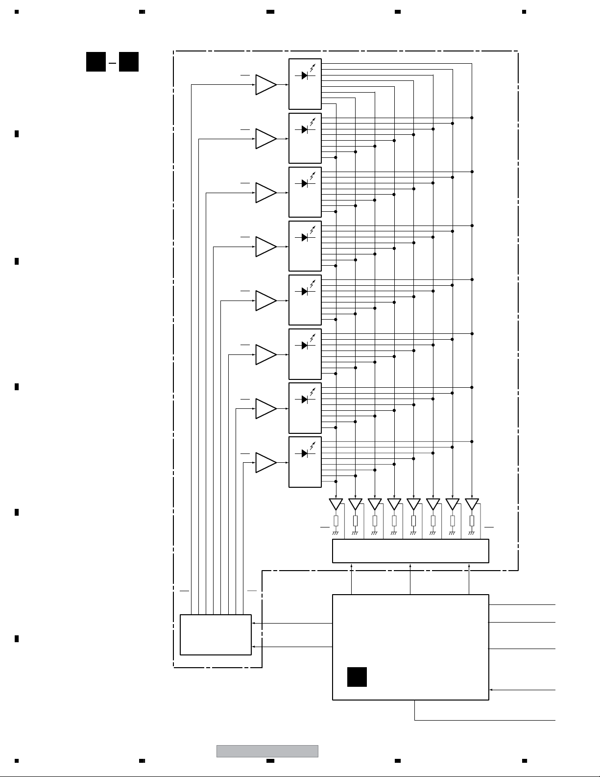
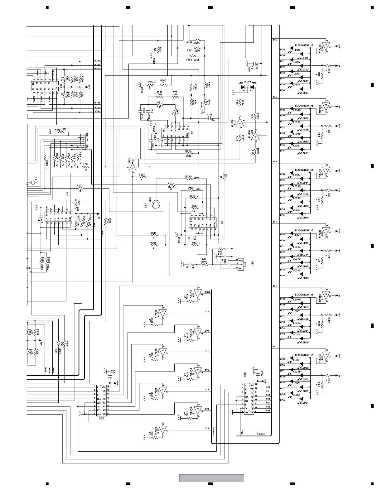
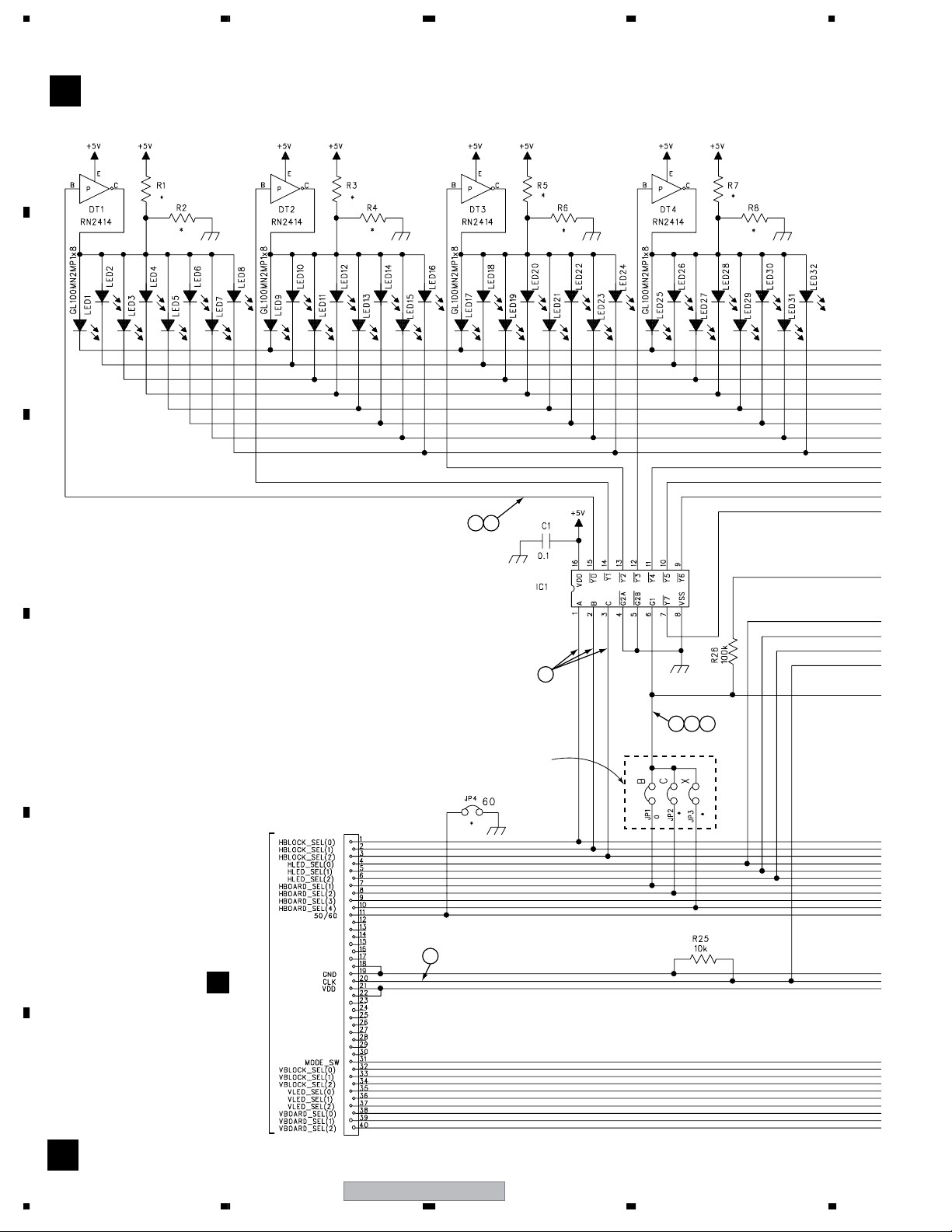
3.1.2 LED AND SENSOR BLOCK DIAGRAM
A
A G
LED-A ASSY –
LED-G ASSY
The illustration shows the block
diagram of the basic LED formation
(applicable to LED-A to LED-G Assys).
For both horizontally and vertically
formatted boards, the block structure is
the same. If any of the three problems
listed below are encountered, use the
B
checkpoints listed below.
• If the unit length of the board is a
problem
For a horizontally formatted board,
the HBOARD_SEL signal may not
be correct. Check the signal.
For a vertically formatted board,
the VBOARD_SEL signal may not
be correct. Check the signal.
• When there is a problem within the
8 LED unit
For a horizontally formatted board,
C
the HBLOCK_SEL signal may not
be correct. Check the signal.
For a vertically formatted board,
the VBLOCK_SEL signal may not
be correct. Check the signal.
Y7
Y6
Y5
Y4
Y3
Y2
DT8
DT7
DT6
DT5
DT4
DT3
LED
(x8)
LED
(x8)
LED
(x8)
LED
(x8)
LED
(x8)
LED
(x8)
• When there is a problem with the
8 LED sensor cycle
For horizontally and vertically
formatted boards, the LED_SEL
signal may not be correct. Check
the signal.
D
E
Y7
3 to 8 line
decoder / invertor
IC1
Y1
Y0
DT2
DT1
Y0
LED
(x8)
LED
(x8)
Y0 Y7
LED Block select
(0, 1, 2)
LED Board select
3 to 8 line decoder / invertor
LED Clock
94.75kHz
IC2
LED Board
select
UCOM
IC15
LED select
(0, 1, 2)
LED-A ASSY
A
F
14
1234
PDK-50HW3
Page 15
5678
Sensor
(x8)
+5V
Sensor
(x8)
+5V
Sensor
(x8)
+5V
Sensor
(x8)
+5V
Sensor
(x8)
+5V
Sensor
(x8)
+5V
Sensor
(x8)
+5V
Sensor
(x8)
+5V
Amp
Amp
Amp
Amp
Amp
Amp
Amp
Amp
Scanner
demux
IC24
Scanner
demux
IC23
Scanner
demux
IC22
Scanner
demux
IC21
Scanner
demux
IC20
Scanner
demux
IC19
Scanner
demux
IC18
Scanner
demux
IC17
Y7
Y6
Y5
Y4
Y3
Y2
Y1
Y0
H N
SENSOR-H ASSY – SENSOR-N ASSY
The illustration shows the block diagram of the sensor board
(applicable to SENSOR-H to SENSOR-N Assys).
For both horizontally and vertically formatted boards, the block
structure is the same. If any of the three problems listed below are
encountered, use the checkpoints listed below.
• If the unit length of the board is a problem
For a horizontally formatted board, the HSDEC_SEL or H_RCV
signal may not be correct. Check the signal.
For a vertically formatted board, the VSDEC_SEL or V_RCV
signal may not be correct. Check the signal.
• When there is a problem within the 8 sensor unit
For a horizontally formatted board, the HSEN_ADR signal may
not be correct. Check the signal.
For a vertically formatted board, the V HSEN_ADR signal may
not be correct. Check the signal.
• When there is a problem with the 8 LED sensor cycle
For a horizontally formatted board, the HSEN_SEL signal may
not be correct. Check the signal.
For a vertically formatted board, the VSEN_SEL signal may not
be correct. Check the signal.
A
B
C
D
Sensor select
(0, 1, 2)
Sensor Board select
Sensor Address select
(0, 1, 2)
X (RCV out)
TP
Adjustable amp
RCV Board select (0, 1)
56
3 to 8 line
decoder / invertor
IC25
4 channel analog
demultiplexer
IC2, IC3
LED-A ASSY
A
Y0
Y7
RCV data from other boards (X0, X1,...)
PDK-50HW3
E
F
15
7
8
Page 16
1234
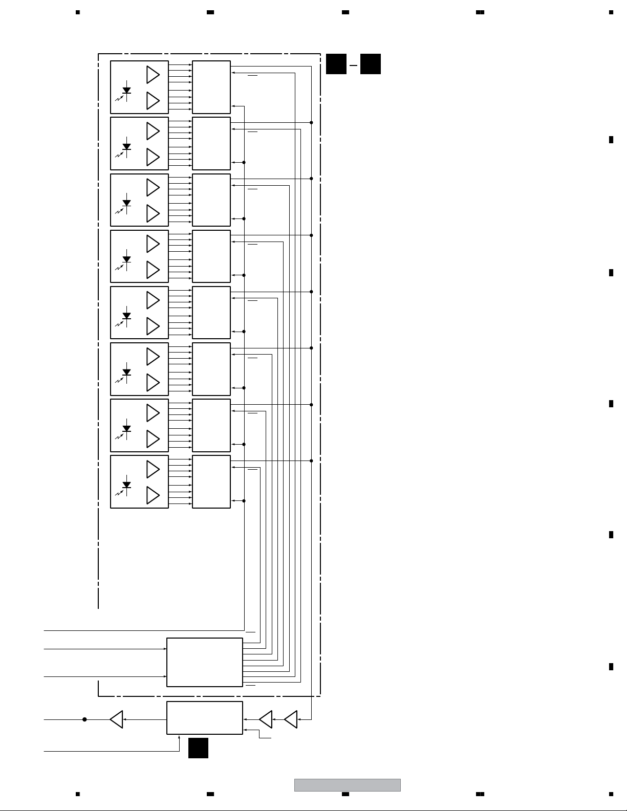
3.2 OVERALL WIRING DIAGRAM
A
SENSOR-K ASSY
K
(BZW1519)
By changing jumper-pin settings on the SENSOR-I, -J, and -K Assy's,
LED-G ASSY
G
B
C
(BZW1515)
CN1
CN4
LED-F ASSY
(BZW1514)
÷
When ordering service parts, be sure to refer to "EXPLODED VIEWS and PARTS LIST" or
"PCB PARTS LIST".
÷
The > mark found on some component parts indicates the importance of the safety factor
of the part. Therefore, when replacing, be sure to use parts of identical designation.
÷
: The power supply is shown with the marked box.
you can use the SENSOR-I, -J, and -K Assy's one in place of another.
Refer to "7.1.4 OPERATION CHECKS USING EXCHANGEABLE ASSY'S"
CN4
CN1
SENSOR-J ASSY
J
(BZW1518)
CN4
F
<BACK SIDE VIEW>
CN1
D
CN4
LED-E ASSY
(BZW1513)
E
E
CN3 CN2
CN5
CN6
LED-D ASSY
D
(BZW1512)
CN1
CN4
LED-C ASSY
C
(BZW1511)
CN1
F
16
1234
By changing jumper-pin settings on the LED-B, and -C Assy's,
you can use the LED-B Assy as the LED-C Assy, and vice versa.
Refer to "7.1.4 OPERATION CHECKS USING EXCHANGEABLE ASSY'S"
PDK-50HW3
Page 17
5678
A
CN1
SENSOR-I ASSY
I
(BZW1517)
<BACK SIDE VIEW>
CN4
CN1
SENSOR-H ASSY
H
(BZW1516)
CN5
CN6
SENSOR-N ASSY
N
(BZW1522)
CN3CN2
CN4
CN1
SENSOR-M ASSY
(BZW1521)
M
B
C
CN4
LED-B ASSY
B
(BZW1510)
CN1
CN2
CN1
CN4
LED-A ASSY
A
(BZW1509)
CN2
CN1
SENSOR-L ASSY
(BZW1520)
L
CN4
CN5
CN6
CN7
CN8
CN9
CN15
CN14CN3
D
E
USB CABLE
(BZD1411)
56
O
(BZW1523)
PDK-50HW3
USB BOARD ASSY
SENSOR HOLDER
SENSOR HOLDER
7
F
17
8
Page 18
1234
Q
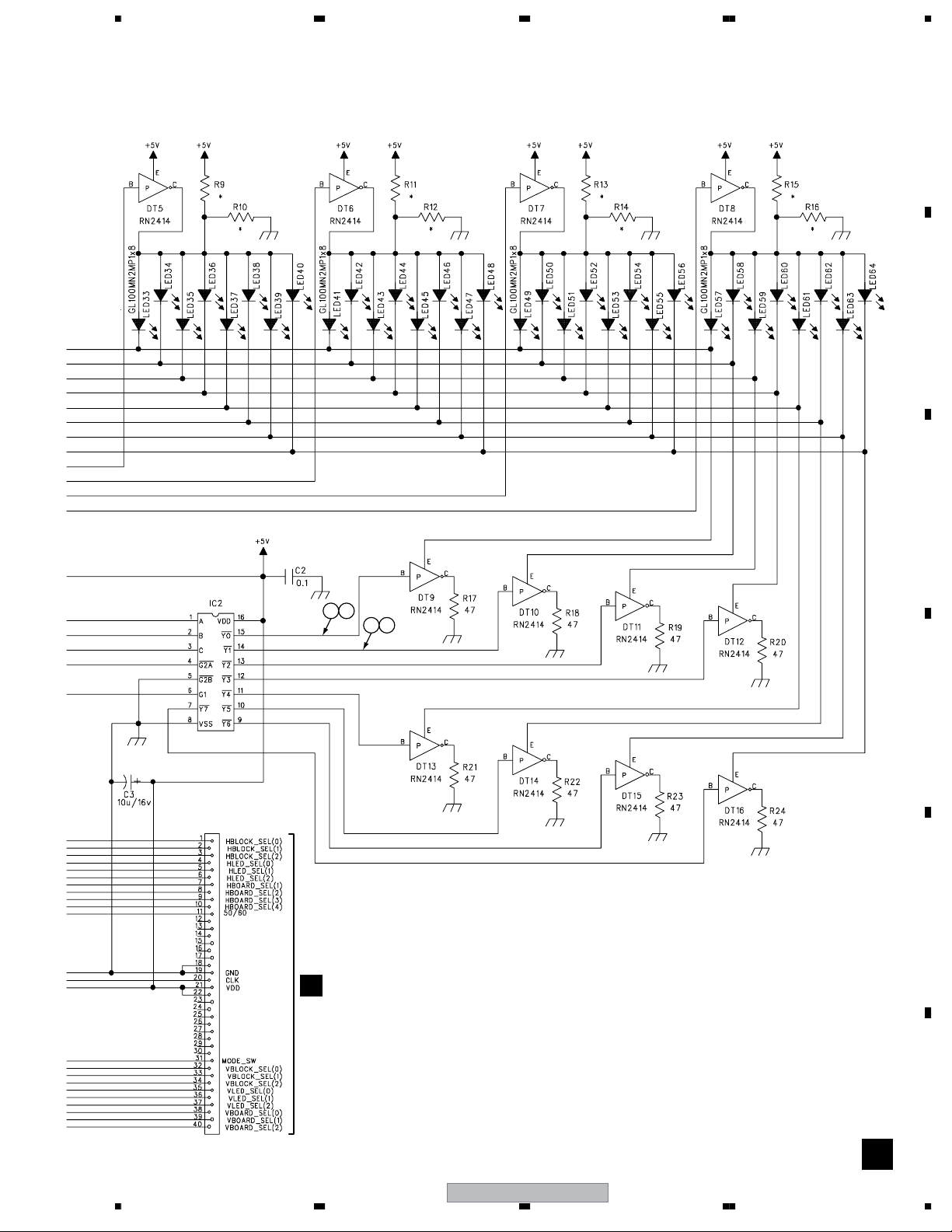
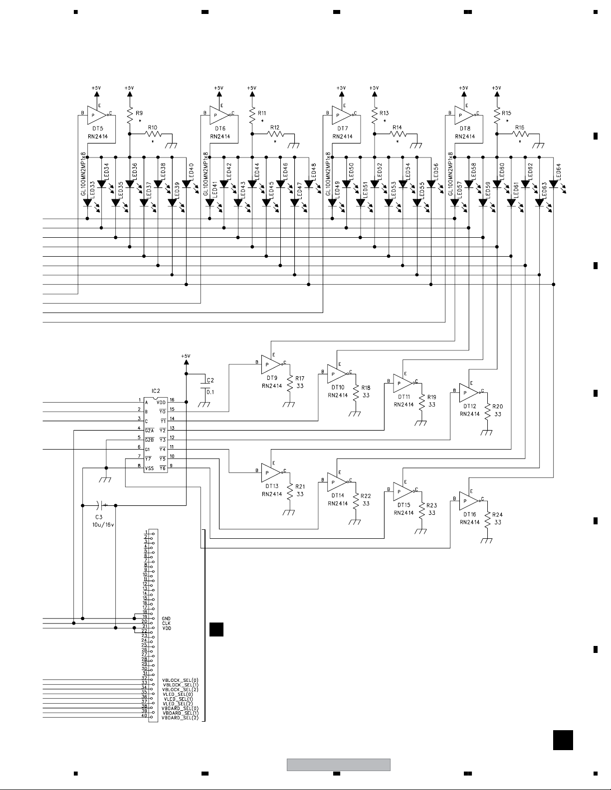
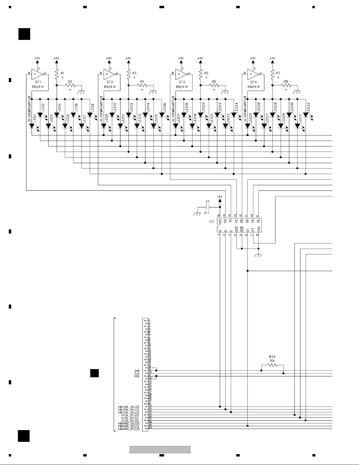
3.3 LED-A ASSY (GUIDE PAGE)
LED-A ASSY (BZW1509)
A
A-a
A
BZT1701
BZT1701
BZQ1765
BZQ1765
CN14
BZK1511
HOLDER
SENSOR
BZQ1747
BZQ1747
B
CN15
BZK1511
HOLDER
SENSOR
BZQ1766
BZQ1747BZQ1747
BZQ1766
BZQ1771
BZQ1766
BZQ1770
BZQ1764
BZQ1764
BZQ1763
C
CN7
BZK1516
L
CN4
L
CN5
L
CN6
D
E
CN8
BZK1512
CN9
BZK1516
AZT1217
BZQ1766
BZQ1746
BZQ1739
BZQ1739
AZT1217
BZQ1739
BZQ1739
BZS1350
BZQ
BZ
BZQ1737 BZQ1737
F
A
18
1234
PDK-50HW3
Page 19
5678
ZQ1764
AZQ1109
BZQ1771
BZQ1768
BZQ1766
BZQ1771
A-b
BZQ1740
BZQ1772
DT1-DT18 : BZQ1768
LED1-LED64 : AZQ1108
A
B
C
1350
BZQ1745
BZQ1743
BZQ1736
BZQ1743
BZT1703
BZT1702
BZQ1743
BZQ1743
CN3
BZK1513
O
CN2
BZQ1772
CN4
BZK1518
D
E
BZQ1743
BZQ1743
BZQ1743
PDK-50HW3
56
CN1
B
F
A
19
7
8
Page 20
1234
3.4 LED-A ASSY
A
BZK1512
BZQ1739
CN5
L
CN8
CN6
A
CN9
BZK1516
AZT1217
BZQ1766
B
BZQ1739
C
BZQ1746
L
BZQ1737 BZQ1737
AZT1217
D
BZQ1739
BZQ1739
E
BZS1350
F
20
1234
PDK-50HW3
Page 21
5678
L
BZQ1739
CN5
L
CN8
BZK1512
CN4
L
CN7
BZK1516
Guide page
2/2
1/2
1/21/2
Detailed page
1/22/2
BZQ1747BZQ1747
BZQ1766
SENSOR
HOLDER
BZK1511
BZT1701
BZQ1765
CN15
BZQ1747
BZQ1766
SENSOR
HOLDER
BZQ1747
BZK1511
BZT1701
CN14
BZQ1765
A
LED-A ASSY (BZW1509)
A
B
C
BZQ1739
BZQ1766
BZQ1771
BZQ1763
D
BZQ1770
BZQ1764
E
BZQ1764
PDK-50HW3
56
F
21
7
8
Page 22
1234
A
B
C
BZQ1743
BZQ1743
BZQ1743
BZQ1745
BZQ1743
BZQ1736
BZQ1743
BZT1703
BZT1702
D
CN3
O
BZK1513
BZQ1743
BZQ1743
CN2
Guide page
2/2
1/2
E
1/21/2
Detailed page
2/22/2
CN4
F
A
B
CN1
22
1234
BZK1518
PDK-50HW3
Page 23
Q
5678
A
BZ
1743
BZQ1771
BZQ1768
BZQ1743
BZQ1766
AZQ1109
B
C
BZQ1771
BZQ1740
BZQ1772
BZQ1772
DT1-DT18 : BZQ1768
LED1-LED64 : AZQ1108
D
E
F
56
PDK-50HW3
23
7
8
Page 24
1234
3.5 LED-B ASSY
LED-B ASSY (BZW1510)
B
A
B
C
9
5
BZQ1772
Block Selector
2
D
Refer to
"7.1.4 OPERATION CHECKS
USING EXCHANGEABLE ASSY'S"
CN1
BZK1517
E
3 4 8
1
CN4
A
F
B
24
1234
PDK-50HW3
Page 25
5678
DT1-DT16 : BZQ1768
LED1-LED64 : AZQ1108
A
B
C
BZQ1772
LED Selector
CN4
BZK1518
C
6
10
CN1
7
11
D
E
56
PDK-50HW3
F
B
25
7
8
Page 26
1234
3.6 LED-C ASSY
LED-C ASSY (BZW1511)
C
A
B
C
BZQ1772
Block Selector
D
Refer to
"7.1.4 OPERATION CHECKS
USING EXCHANGEABLE ASSY'S"
CN1
BZK1517
E
CN4
B
F
C
26
1234
PDK-50HW3
Page 27

5678
DT1-DT16 : BZQ1768
LED1-LED64 : AZQ1108
A
B
C
BZQ1772
LED Selector
CN4
BZK1518
CN1
D
PDK-50HW3
56
D
E
F
C
27
7
8
Page 28
1234
3.7 LED-D ASSY
LED-D ASSY (BZW1512)
D
A
B
C
BZQ1772
Block Selector
CN2
BZK1511
D
CN1
BZK1517
E
CN4
C
F
D
28
1234
PDK-50HW3
Page 29

5678
DT1-DT16 : BZQ1768
LED1-LED64 : AZQ1108
A
B
C
BZQ1772
LED Selector
CN5
BZK1512
CN2
E
CN6
BZK1515
CN3
E
PDK-50HW3
56
D
E
F
D
29
7
8
Page 30

1234
3.8 LED-E ASSY
LED-E ASSY (BZW1513)
E
A
B
C
BZQ1772
Block Selector
D
E
CN2
BZK1512
CN5
D
CN3
BZK1515
CN6
D
F
E
30
1234
PDK-50HW3
Page 31
5678
DT1-DT16 : BZQ1768
LED1-LED64 : AZQ1108
A
B
C
BZQ1772
LED Selector
CN1
F
CN4
BZK1518
PDK-50HW3
56
D
E
F
E
31
7
8
Page 32
1234
3.9 LED-F ASSY
LED-F ASSY (BZW1514)
F
A
B
C
BZQ1772
Block Selector
D
CN1
BZK1517
E
CN4
E
F
F
32
1234
PDK-50HW3
Page 33

5678
DT1-DT16 : BZQ1768
LED1-LED64 : AZQ1108
A
B
C
BZQ1772
LED Selector
CN4
BZK1518
CN1
G
PDK-50HW3
56
D
E
F
F
33
7
8
Page 34

1234
3.10 LED-G ASSY
LED-G ASSY (BZW1515)
G
A
B
C
BZQ1772
Block Selector
D
CN1
BZK1517
BZQ1772
LED Selector
E
CN4
F
F
G
34
1234
PDK-50HW3
Page 35

5678
A
LED1-LED16 : AZQ1108
B
C
D
E
DT1-DT10 : BZQ1768
PDK-50HW3
56
F
G
35
7
8
Page 36
1234
3.11 SENSOR-H ASSY
SEOSOR-H ASSY (BZW1516)
H
A
B
C
D
BZQ1769
AZT1217
E
BZQ1769
BZQ1766
CN1
BZK1517
BZQ1769
2
3
BZQ1738
BZQ1769
1
CN4
I
F
H
36
1234
PDK-50HW3
Page 37

5678
PD1-PD64 : AZQ1107
A
B
C
BZQ1769
CN5
BZK1513
BZQ1769 BZQ1769
TR1-TR64 : BZQ1747
CN3
N
CN6
BZK1516
CN2
N
PDK-50HW3
56
D
BZQ1769
E
F
H
37
7
8
Page 38
1234
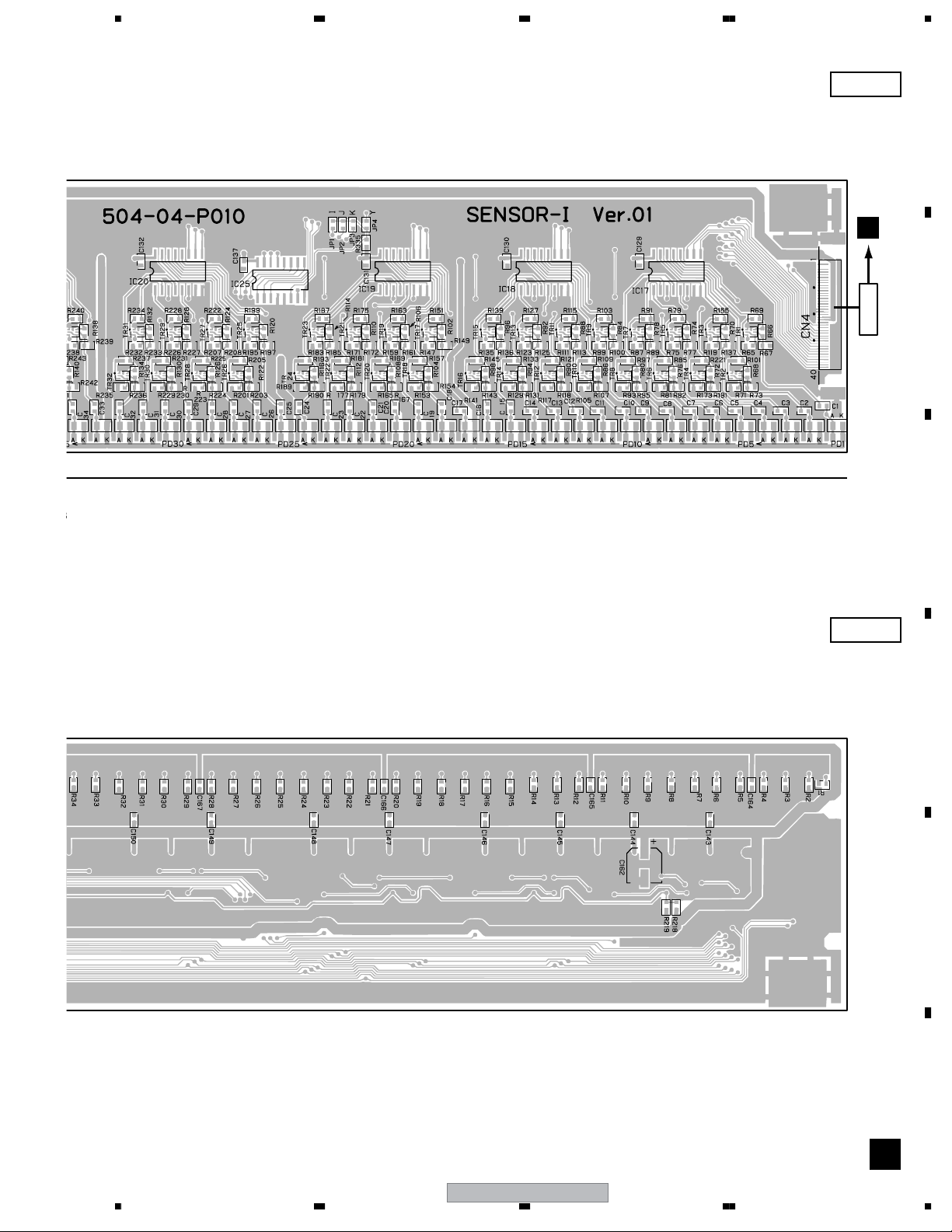
3.12 SENSOR-I ASSY
SENSOR-I ASSY (BZW1517)
I
A
B
C
D
BZQ1769BZQ1769BZQ1769BZQ1769
AZT1217
E
BZQ1766
CN1
BZK1517
BZQ1772
BZQ1738
CN4
J
F
Refer to "7.1.4
OPERATION
CHECKS USING
EXCHANGEABLE
ASSY'S"
I
38
1234
PDK-50HW3
Page 39

5678
PD1-PD64 : AZQ1107
A
B
C
BZQ1769
CN4
BZK1518
TR1-TR64 : BZQ1747
CN1
H
PDK-50HW3
56
D
BZQ1769BZQ1769BZQ1769
E
F
I
39
7
8
Page 40
1234
3.13 SENSOR-J ASSY
SENSOR-J ASSY (BZW1518)
J
A
B
C
D
BZQ1769BZQ1769BZQ1769
AZT1217
E
BZQ1766
CN1
BZK1517
BZQ1769
BZQ1772
BZQ1738
CN4
K
F
Refer to "7.1.4
OPERATION
CHECKS USING
EXCHANGEABLE
ASSY'S"
J
40
1234
PDK-50HW3
Page 41
5678
PD1-PD64 : AZQ1107
A
B
C
BZQ1769
CN4
BZK1518
BZQ1769BZQ1769
TR1-TR64 : BZQ1747
CN1
I
PDK-50HW3
56
D
BZQ1769
E
F
J
41
7
8
Page 42
1234
3.14 SENSOR-K ASSY
SENSOR-K ASSY (BZW1519)
K
A
B
C
D
BZQ1769
AZT1217
E
BZQ1766
BZQ1769BZQ1769BZQ1769
BZQ1772
BZQ1738
F
Refer to "7.1.4
OPERATION
CHECKS USING
EXCHANGEABLE
ASSY'S"
K
42
1234
PDK-50HW3
Page 43

5678
PD1-PD64 : AZQ1107
A
B
C
TR1-TR64 : BZQ1747
CN4
BZK1518
CN1
J
PDK-50HW3
56
D
BZQ1769BZQ1769BZQ1769BZQ1769
E
F
K
43
7
8
Page 44

1234
3.15 SENSOR-L ASSY
SENSOR-L ASSY (BZW1520)
L
A
B
C
D
BZQ1769
AZT1217
E
BZQ1766
CN1
BZK1517
BZQ1769BZQ1769BZQ1769
BZQ1772
BZQ1738
CN2
M
F
L
44
1234
PDK-50HW3
Page 45

5678
PD1-PD64 : AZQ1107
A
B
C
TR1-TR64 : BZQ1747
CN4
BZK1516
CN7
A
CN5
BZK1512
A
CN6
BZK1516
A
CN8
CN9
PDK-50HW3
56
D
BZQ1769BZQ1769BZQ1769BZQ1769
E
F
L
45
7
8
Page 46
1234
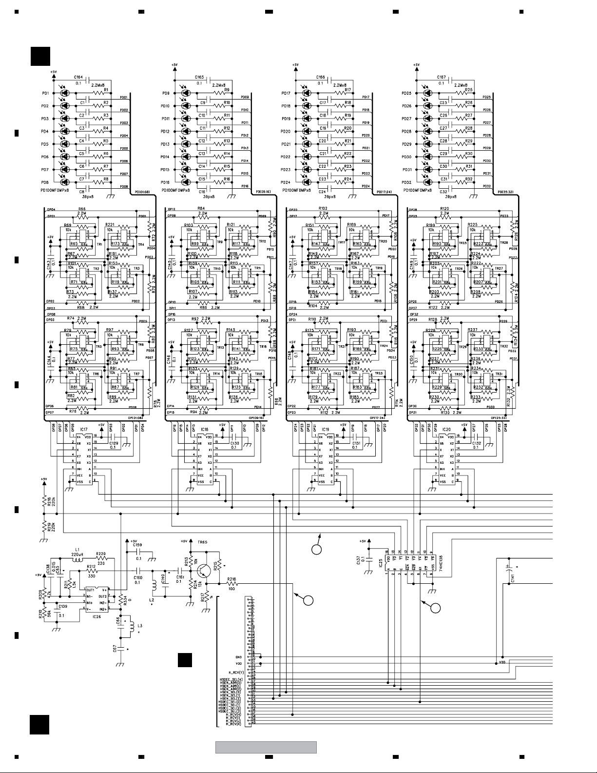
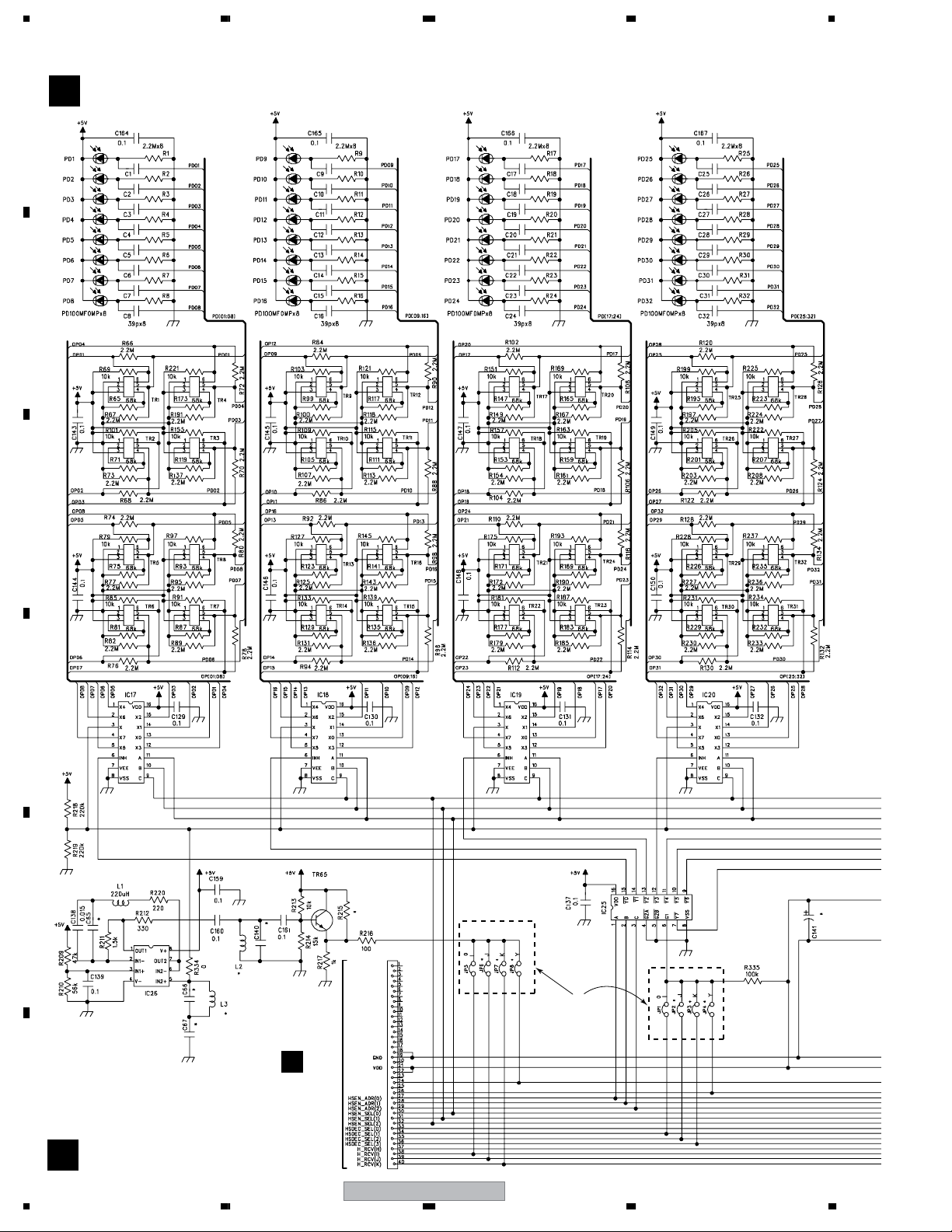
3.16 SENSOR-M ASSY
SENSOR-M ASSY (BZW1521)
M
A
B
C
D
BZQ1769BZQ1769BZQ1769BZQ1769
AZT1217
E
BZQ1766
CN1
BZK1517
BZQ1772
BZQ1738
CN4
N
F
M
46
1234
PDK-50HW3
Page 47

5678
PD1-PD64 : AZQ1107
A
B
C
TR1-TR64 : BZQ1747
CN2
BZK1518
CN1
L
PDK-50HW3
56
D
BZQ1769BZQ1769BZQ1769BZQ1769
E
F
M
47
7
8
Page 48
1234
3.17 SENSOR-N ASSY
A
B
PD1-PD16 : AZQ1107
SENSOR-N ASSY (BZW1522)
N
C
TR1-TR16 : BZQ1747
D
BZQ1769BZQ1769
AZT1217
E
BZQ1766
BZQ1772
CN4
BZK1518
BZQ1738
CN3
BZK1513
CN5
H
CN2
H
BZK1516
CN6
F
M
CN1
N
48
1234
PDK-50HW3
Page 49
5678
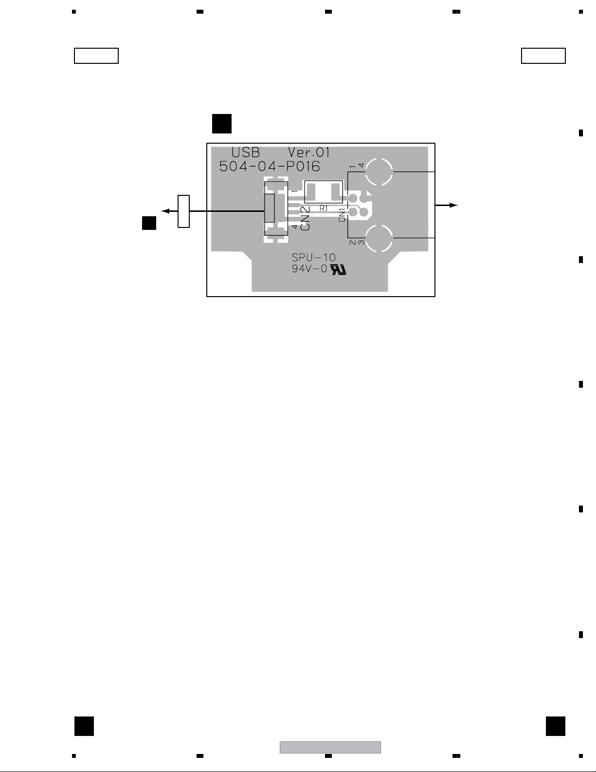
3.18 USB BOARD ASSY
USB BOARD ASSY (BZW1523)
O
A
(RED)
(WHT)
(GRN)
(BLK)
CN1
BZK1510
BZQ1759
CN2
BZK1513
CN3USB CABEL SIDE
A
B
C
D
56
PDK-50HW3
E
F
O
49
7
8
Page 50
1234
3.19 PEN PCB ASSY
PEN PCB ASSY (BZW1524)
P
A
AZT1219
B
BZQ1767
BZC2486
C
BZQ1762
BZQ1761
D
BZQ1744
E
AZQ1110
F
P
50
1234
AZS1142 AZS1140
BUTTON 2
(M)
PDK-50HW3
BUTTON 1
(R)
PEN
(L)
Page 51
5678
A
B
BZQ1742
C
BZC2483
D
AZP1163
E
56
PDK-50HW3
F
P
51
7
8
Page 52

1234
3.20 WAVEFORMS
Note : The encircled numbers denote measuring point in the schematic diagram.
A
LED-B ASSY
B
CN1 - pin 20 (CLK (100kHz))
1
V: 2V/div. H: 5µsec/div.
IC1 - pin 6 (BOARD_SELECT)
4
V: 5V/div. H: 1msec/div.
IC1 - pin 15 (BLOCK Y0)
5
V: 5V/div. H: 1msec/div.
IC2 - pin 15 (LED_SELECT Y0)
6
V: 5V/div. H: 1msec/div.
IC2 - pin 14 (LED_SELECT Y1)
7
V: 5V/div. H: 1msec/div.
B
4
5
6
7
IC1 - pin 1, 2, 3 (HBLOCK_SEL (0, 1, 2))
2
C
V: 5V/div. H: 1msec/div.
IC1 - pin 6 (BOARD_SELECT)
8
V: 5V/div. H: 1msec/div.
IC1 - pin 15 (BLOCK Y0)
9
V: 5V/div. H: 1msec/div.
IC2 - pin 15 (LED_SELECT Y0)
10
V: 5V/div. H: 1msec/div.
IC2 - pin 14 (LED_SELECT Y1)
11
V: 5V/div. H: 1msec/div.
8
9
D
10
11
IC1 - pin 6 (HBOARD_SEL (1))
3
V: 5V/div. H: 10msec/div.
E
SENSOR-H ASSY
H
IC25 - pin 6 (HSDEC_SEL (φ))
1
V: 5V/div. H: 5msec/div.
IC25 - pin 15 (HSDEC_Yφ)
2
V: 5V/div. H: 5msec/div.
CN1 - pin 37 (H_RCV (H))
3
V: 0.5V/div. H: 5msec/div.
1
2
F
3
52
1234
PDK-50HW3
Page 53
5678
4. PCB CONNECTION DIAGRAM
NOTE FOR PCB DIAGRAMS :
1. Part numbers in PCB diagrams match those in the schematic
diagrams.
2. A comparison between the main parts of PCB and schematic
diagrams is shown below.
Symbol In PCB
Diagrams
BCE
BCE
D
Symbol In Schematic
Diagrams
BCEBCE
BCE
DGGSS
BCE
DGS
Part Name
Transistor
Transistor
with resistor
Field effect
transistor
Resistor array
3-terminal
regulator
3. The parts mounted on this PCB include all necessary parts for
several destinations.
For further information for respective destinations, be sure to
check with the schematic diagram.
4. View point of PCB diagrams.
Connector
Capacitor
SIDE A
P.C.Board
Chip Part
SIDE B
A
B
C
D
E
56
PDK-50HW3
F
53
7
8
Page 54
1234
N
3
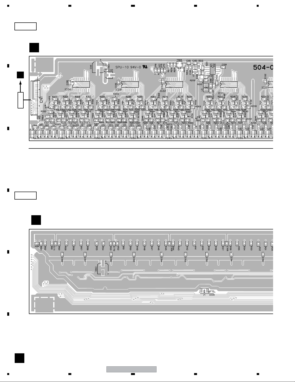
4.1 LED-A ASSY
SIDE A
A
CN4
L
B
CN7
L
CN5
LED-A ASSY
CN8 CN1
A
C
D
E
SIDE B
CN6
L
CN9
IC6
IC7
VR3
IC8 IC9 IC11 IC12
TR17
VR1 VR2 VR4 VR5
IC1 IC2
DT18 DT17 IC30 IC29
IC28
A
TR1
TR4DT1
TR2
IC3
LED-A ASSY
IC4
TR3
IC5
DT2 DT3 DT4
IC10
TR16
IC13
IC14
TR15 TR14
CN
O
C
F
A
54
1234
PDK-50HW3
Page 55

5678
DT4
To
SENSOR
HOLDER
CN2
IC15 IC16 IC17 IC21
DT5
IC18
IC19 IC20
CN15
TR5 TR6
DT6
IC22
IC23 IC24 IC25 IC26
DT7
TR10 TR12 TR13
DT8 DT9
DT10
DT11
To
SENSOR
HOLDER
CN14
DT13 DT15
DT12
DT14
SIDE A
A
CN1
B
B
CN4
C
15 IC27 DT16TR14
SIDE B
D
E
CN3
O
CN2
56
PDK-50HW3
F
A
55
7
8
Page 56
1234
4.2 LED-B and LED-C ASSYS
SIDE A
A
LED-B ASSY
B
CN4
A
B
CN1
DT1 DT2 DT3 DT4 DT5
C
LED-C ASSY
D
C
CN4
B
CN1
E
F
56
DT1 DT2 DT3 DT4 DT5
B C
PDK-50HW3
1234
Page 57

5678
SIDE A
A
CN1
C
B
CN4
DT5 IC1 IC2
DT6
DT9
DT10
DT11
DT12
DT13
DT15 DT7 DT8
DT14
DT16
C
D
CN1
D
CN4
E
DT5 IC1 IC2
56
DT6
DT9
DT10
DT11
DT12
DT13
DT15 DT7 DT8
DT14
DT16
PDK-50HW3
F
CB
57
7
8
Page 58
1234
4.3 LED-D and LED-F ASSYS
SIDE A
A
LED-D ASSY
D
CN4
C
B
CN1
DT1 DT2 DT3 DT4 DT5
C
LED-F ASSY
D
F
CN4
E
CN1
E
F
58
DT1 DT2 DT3 DT4 DT5
D F
PDK-50HW3
1234
Page 59

5678
SIDE A
A
DT5 IC1 IC2
DT6
DT9
DT10
DT11
DT12
DT13
DT15 DT7 DT8
DT14
DT16
CN2
CN2
E
CN5
B
CN6
CN3
E
C
DT5 IC1 IC2
56
DT6
DT9
DT10
DT11
DT12
DT13
DT15 DT7 DT8
DT14
DT16
PDK-50HW3
D
CN1
G
CN4
E
F
FD
59
7
8
Page 60

1234
4.4 LED-E ASSY
SIDE A
A
LED-E ASSY
E
CN6
D
B
CN3
CN2
D
CN5
C
D
E
SIDE B
LED-E ASSY
E
DT1 DT2 DT3 DT4 DT5
F
E
60
1234
PDK-50HW3
Page 61

5678
SIDE A
A
CN1
F
DT5 IC1 IC2
DT6
DT9
DT10
DT11
DT12
DT13
DT15 DT7 DT8
DT14
DT16
CN4
B
C
SIDE B
D
56
PDK-50HW3
E
F
E
61
7
8
Page 62
1234
4.5 LED-G ASSY
SIDE A SIDE A
LED-G ASSY
A
G
CN4
F
B
CN1
C
DT1 DT2 DT3 DT4 DT5 DT6
IC2IC1
DT7 DT8 DT9 DT10
SIDE B SIDE B
LED-G ASSY
G
D
E
F
G G
62
1234
PDK-50HW3
Page 63

5678
A
B
C
D
E
56
PDK-50HW3
F
63
7
8
Page 64

1234
0
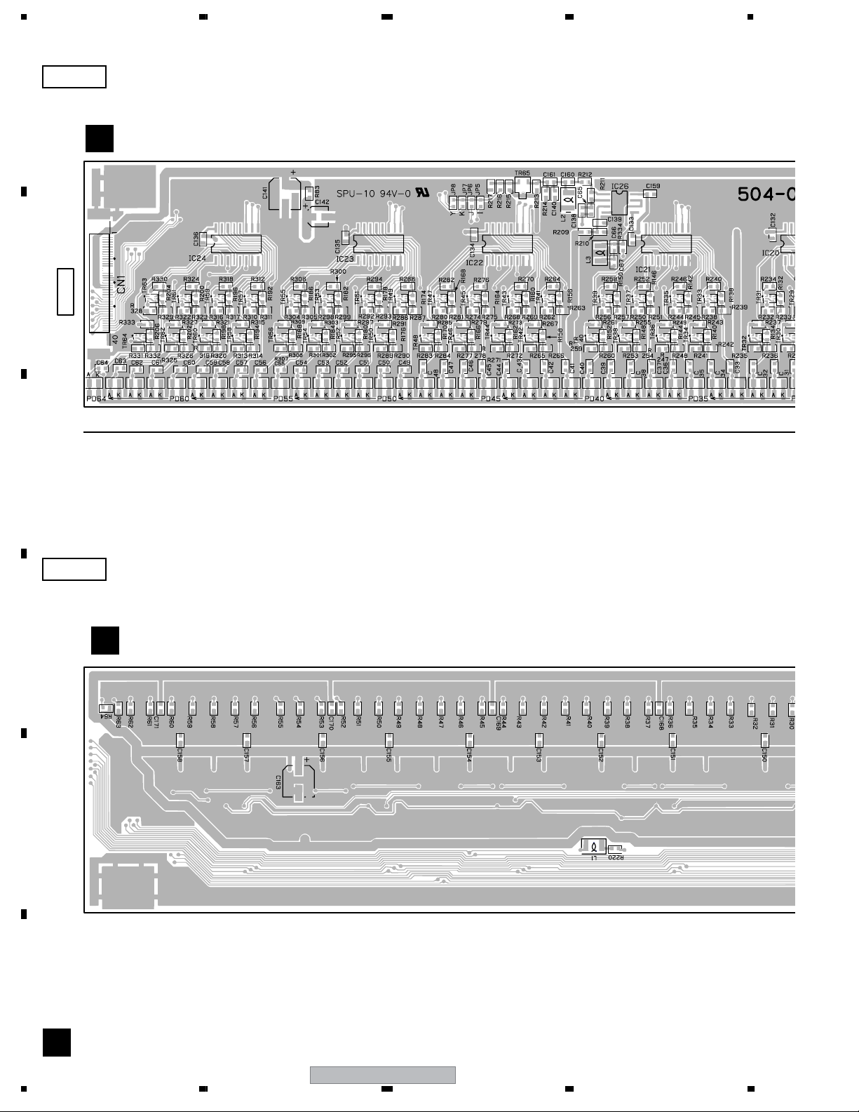
4.6 SENSOR-H ASSY
SIDE A
A
SENSOR-H ASSY
H
CN4
I
B
CN1
C
D
E
SIDE B
IC24
TR63
TR64 TR62 TR60 TR58 TR56 TR54 TR52 TR50
SENSOR-H ASSY
H
TR61 TR59 TR57 TR55 TR53 TR51 TR49
IC23 IC22 IC21IC26TR65
TR47 TR45 TR43 TR41 TR39 TR37 TR35 TR33
TR48 TR46 TR44 TR42 TR40 TR38 TR36 TR34
TR31 T
TR32 TR3
F
H
64
1234
PDK-50HW3
Page 65

5678
SIDE A
N
CN3
CN5
A
CN2
N
IC20 IC25 IC19 IC18 IC17
33
TR31 TR29 TR27 TR25 TR23 TR21 TR19 TR17 TR15 TR13 TR11 TR9 TR7 TR5 TR3 TR1
TR32 TR30 TR28 TR26 TR24 TR22 TR20 TR18 TR16 TR14 TR12 TR10 TR8 TR6 TR4 TR2
CN6
SIDE B
B
C
D
56
PDK-50HW3
E
F
H
65
7
8
Page 66
1234
3
T
4.7 SENSOR-I ASSY
SIDE A
A
SENSOR-I ASSY
I
CN4
J
B
CN1
C
D
E
SIDE B
IC24
TR63
TR64 TR62 TR60 TR58 TR56 TR54 TR52 TR50
SENSOR-I ASSY
I
TR61 TR59 TR57 TR55 TR53 TR51 TR49
IC23 IC22 IC21IC26TR65
TR47 TR45 TR43 TR41 TR39 TR37 TR35 TR33
TR48 TR46 TR44 TR42 TR40 TR38 TR36 TR34
TR31
TR32 TR
F
I
66
1234
PDK-50HW3
Page 67
5678
SIDE A
A
CN1
H
IC20 IC25 IC19 IC18 IC17
R33
4
TR31 TR29 TR27 TR25 TR23 TR21 TR19 TR17 TR15 TR13 TR11 TR9 TR7 TR5 TR3 TR1
TR32 TR30 TR28 TR26 TR24 TR22 TR20 TR18 TR16 TR14 TR12 TR10 TR8 TR6 TR4 TR2
CN4
SIDE B
B
C
D
56
PDK-50HW3
E
F
I
67
7
8
Page 68

1234
0
T
4.8 SENSOR-J ASSY
SIDE A
A
SENSOR-J ASSY
J
CN4
K
B
CN1
C
D
E
SIDE B
IC24
TR63
TR64 TR62 TR60 TR58 TR56 TR54 TR52 TR50
SENSOR-J ASSY
J
TR61 TR59 TR57 TR55 TR53 TR51 TR49
IC23 IC22 IC21IC26TR65
TR47 TR45 TR43 TR41 TR39 TR37 TR35 TR33
TR48 TR46 TR44 TR42 TR40 TR38 TR36 TR34
TR31
TR32 TR3
F
J
68
1234
PDK-50HW3
Page 69

5678
SIDE A
A
CN1
I
IC20 IC25 IC19 IC18 IC17
33
TR31 TR29 TR27 TR25 TR23 TR21 TR19 TR17 TR15 TR13 TR11 TR9 TR7 TR5 TR3 TR1
TR32 TR30 TR28 TR26 TR24 TR22 TR20 TR18 TR16 TR14 TR12 TR10 TR8 TR6 TR4 TR2
CN4
SIDE B
B
C
D
56
PDK-50HW3
E
F
J
69
7
8
Page 70
1234
0
T
4.9 SENSOR-K ASSY
SIDE A
A
SENSOR-K ASSY
K
B
CN1
C
D
E
SIDE B
IC24
TR63
TR64 TR62 TR60 TR58 TR56 TR54 TR52 TR50
SENSOR-K ASSY
K
TR61 TR59 TR57 TR55 TR53 TR51 TR49
IC23 IC22
TR47 TR45 TR43 TR41 TR39 TR37 TR35 TR33
TR48 TR46 TR44 TR42 TR40 TR38 TR36 TR34
IC26TR65
IC21
TR31
TR32 TR3
F
K
70
1234
PDK-50HW3
Page 71

5678
SIDE A
A
CN1
J
IC20 IC25 IC19 IC18 IC17
33
TR31 TR29 TR27 TR25 TR23 TR21 TR19 TR17 TR15 TR13 TR11 TR9 TR7 TR5 TR3 TR1
TR32 TR30 TR28 TR26 TR24 TR22 TR20 TR18 TR16 TR14 TR12 TR10 TR8 TR6 TR4 TR2
CN4
SIDE B
B
C
D
56
PDK-50HW3
E
F
K
71
7
8
Page 72
1234
0
R
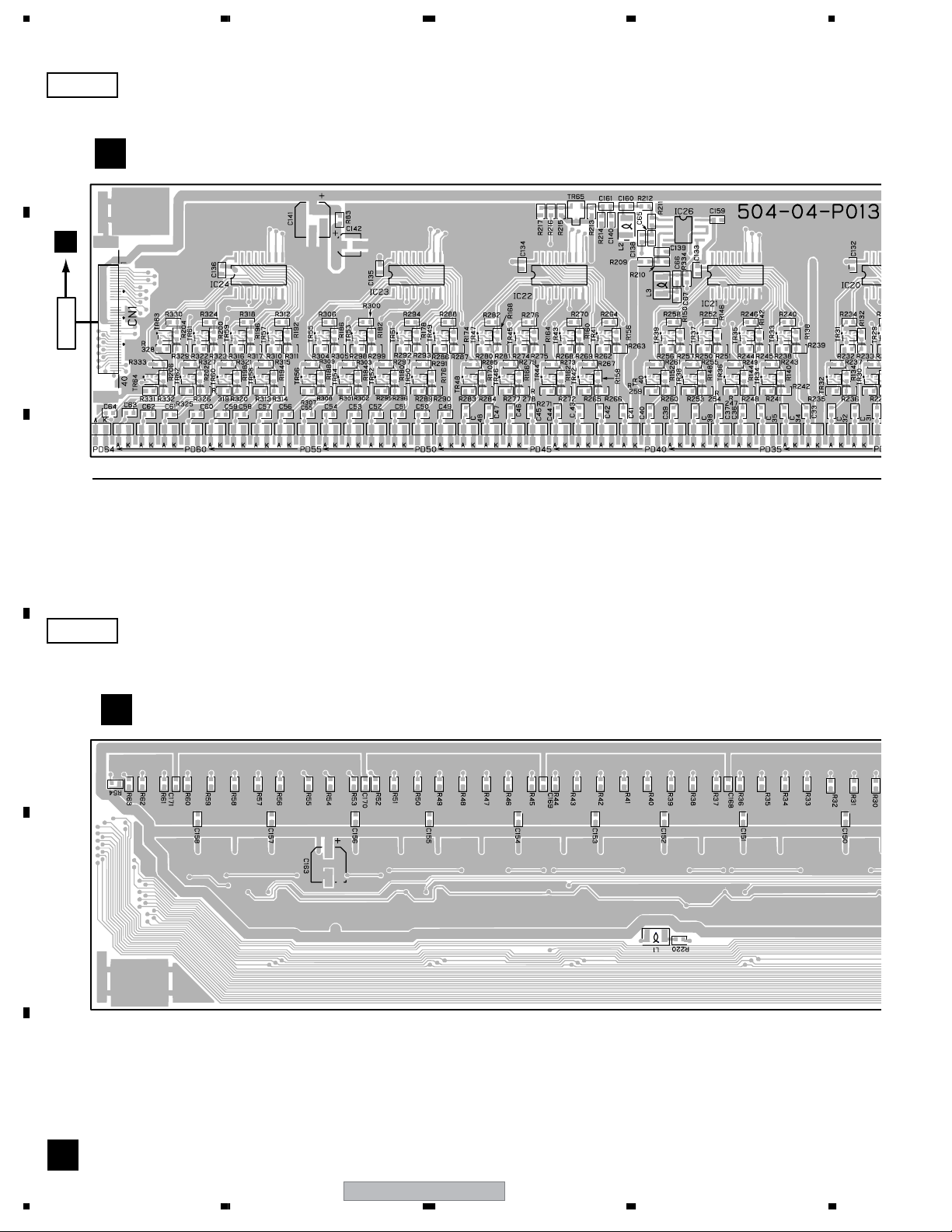
4.10 SENSOR-L ASSY
SIDE A
A
SENSOR-L ASSY
L
CN2
M
B
CN1
C
D
E
SIDE B
IC24
TR63
TR64 TR62 TR60 TR58 TR56 TR54 TR52 TR50
SENSOR-L ASSY
L
TR61 TR59 TR57 TR55 TR53 TR51 TR49
IC23 IC22
TR47 TR45 TR43 TR41 TR39 TR37 TR35 TR33
TR48 TR46 TR44 TR42 TR40 TR38 TR36 TR34
IC26TR65
IC21
TR31 T
TR32 TR3
F
L
72
1234
PDK-50HW3
Page 73
5678
SIDE A
A
CN8
CN5
A
CN7
A
IC20 IC25 IC19 IC18 IC17
33
TR31 TR29 TR27 TR25 TR23 TR21 TR19 TR17 TR15 TR13 TR11 TR9 TR7 TR5 TR3 TR1
TR32 TR30 TR28 TR26 TR24 TR22 TR20 TR18 TR16 TR14 TR12 TR10 TR8 TR6 TR4 TR2
CN4
SIDE B
B
C
D
56
PDK-50HW3
CN9
A
CN6
E
F
L
73
7
8
Page 74
1234
0
4.11 SENSOR-M ASSY
SIDE A
A
SENSOR-M ASSY
M
B
C
D
E
SIDE B
CN4
N
CN1
IC24
TR63
TR64 TR62 TR60 TR58 TR56 TR54 TR52 TR50
M
TR61 TR59 TR57 TR55 TR53 TR51 TR49
SENSOR-M ASSY
IC23 IC22
TR47 TR45 TR43 TR41 TR39 TR37 TR35 TR33
TR48 TR46 TR44 TR42 TR40 TR38 TR36 TR34
IC26TR65
IC21
TR31 T
TR32 TR3
F
M
74
1234
PDK-50HW3
Page 75
5678
SIDE A
A
CN1
L
B
CN2
IC20 IC25 IC19 IC18 IC17
33
TR31 TR29 TR27 TR25 TR23 TR21 TR19 TR17 TR15 TR13 TR11 TR9 TR7 TR5 TR3 TR1
TR32 TR30 TR28 TR26 TR24 TR22 TR20 TR18 TR16 TR14 TR12 TR10 TR8 TR6 TR4 TR2
C
SIDE B
D
E
56
PDK-50HW3
F
M
75
7
8
Page 76
1234
4.12 SENSOR-N ASSY
SIDE A SIDE A
H
A
CN5
CN3
SENSOR-N ASSY
N
CN6
H
B
CN2
C
TR14
TR15 TR13 TR11 TR8 TR7 TR5 TR3 TR1TR16
IC25 IC26 TR65
TR12 TR10 TR9 TR6 TR4 TR2
SIDE B SIDE B
SENSOR-N ASSY
N
D
E
CN1
M
CN4
F
N N
76
1234
IC18 IC17
PDK-50HW3
Page 77
5678
4.13 USB BOARD ASSY
SIDE A SIDE A
USB BOARD ASSY
O
CN3
A
CN2
USB CABLE
A
B
C
D
E
O O
56
PDK-50HW3
7
8
F
77
Page 78

1234
4.14 PEN PCB ASSY
SIDE A SIDE A
A
PEN PCB ASSY
P
B
SIDE B SIDE B
C
PEN PCB ASSY
P
VR2 VR1
D
E
IC2 TR2
IC3 IC1
TR1
F
P P
78
1234
PDK-50HW3
Page 79

5678
5. PCB PARTS LIST
NOTES:
Parts marked by "NSP" are generally unavailable because they are not in our Master Spare Parts List.
The mark found on some component parts indicates the importance of the safety factor of the part.
Therefore, when replacing, be sure to use parts of identical designation.
When ordering resistors, first convert resistance values into code form as shown in the following examples.
Ex.1 When there are 2 effective digits (any digit apart from 0), such as 560 ohm and 47k ohm (tolerance is shown by J=5%,
and K=10%).
560 Ω
47k Ω
0.5 Ω
1 Ω
56 x 10
47 x 10
R50
1R0
1
3
Ex.2 When there are 3 effective digits (such as in high precision metal film resistors).
5.62k Ω
1
Mark No. Description Part No.
LIST OF ASSEMBLIES
1..LED-A ASSY BZW1509
1..LED-B ASSY BZW1510
1..LED-C ASSY BZW1511
1..LED-D ASSY BZW1512
1..LED-E ASSY BZW1513
1..LED-F ASSY BZW1514
1..LED-G ASSY BZW1515
1..SENSOR-H ASSY BZW1516
1..SENSOR-I ASSY BZW1517
1..SENSOR-J ASSY BZW1518
1..SENSOR-K ASSY BZW1519
1..SENSOR-L ASSY BZW1520
1..SENSOR-M ASSY BZW1521
1..SENSOR-N ASSY BZW1522
1..USB BOARD ASSY BZW1523
1..PEN PCB ASSY BZW1524
561
473
5621
RD1/4PU J
RD1/4PU J
RN2H K
RS1P K
RN1/4PC F562 x 10
561
473
R50
1R0
5621
Mark No. Description Part No.
SWITCHES
SW1 BZS1350
COILS AND FILTERS
L1,L2 AZT1217
L3,L4 BZT1701
CAPACITORS
NSP C118 CCSRCH100D50
NSP C1-C4,C6-C7,C9,C10,C12 CKSRYB104K25
NSP C13,C15-C21,C23,C25-C27 CKSRYB104K25
NSP C29-C32,C34-36,C39-40 CKSRYB104K25
NSP C42,C47-C49,C56,C58,C61 CKSRYB104K25
NSP C62,C65,C67,C69,C72-C74 CKSRYB104K25
NSP C76,C78,C84-C87,C91,C95 CKSRYB104K25
NSP C97,C98,C100-C107,C113 CKSRYB104K25
NSP C114,C116,C117 CKSRYB104K25
NSP C22,C24,C44,C57,C92,C94 CCSRCH103K50
A
B
C
Mark No. Description Part No.
LED-A ASSY
A
SEMICONDUCTORS
IC1,IC6,IC7,IC28 BZQ1739
IC10 BZQ1745
IC11 BZQ1740
IC12-IC14,IC16-IC19 BZQ1743
NSP IC15 BZQ1736
IC20,IC26 BZQ1772
IC21 BZQ1763
IC2,IC3,IC22,IC30 TC74HC4066AF
IC24 BZQ1770
IC25,IC29 BZQ1764
IC27 BZQ1741
IC4,IC5 BZQ1737
IC8,IC9,IC23 BZQ1771
DT1-DT18,TR17 BZQ1768
TR14 BZQ1746
TR5,TR9,TR12,TR15,TR16 BZQ1766
TR6,TR10 BZQ1765
TR7,TR8,TR11,TR13 BZQ1747
D2-D4 1SS184
LED1-LED64 AZQ1108
LED65 AZQ1109
56
NSP C111,C112 CCSRCH103K50
NSP C28,C115 CCSRCH271J50
NSP C37,C64,C75,C80,C96 CEVQW100M25
NSP C38,C41,C55,C60 CCSRCH561J50
NSP C43,C59,C901 CCSRCH101J50
NSP C45,C54 CKSRYB223K50
NSP C46,C53 CKSRYB153K50
NSP C50,C68 CKSRYB333K25
NSP C51 • • • • • •
NSP C52 CFHBSP683J16
NSP C63,C71 CEVQW101M6R3
NSP C77,C79 CCSRCH220J50
NSP C8,C33,C66,C70,C83 CEVQW470M16
NSP C81-82 CCSRCH150J50
NSP C88-90,C93 CCSRCH152J50
RESISTORS
NSP R102,R107-R115,R185-R192 RS1/10SR223J
NSP R195-R198,R223-R225,R228-R234 RS1/10SR223J
NSP R236,R237,R144,R158 RS1/10SR223J
NSP R105,R106 RS1/10SR101J
NSP R122,R160,R298 RS1/10SR154J
NSP R123,R153 RS1/10SR221J
NSP R126,R127,R130,R131,R159 RS1/10SR225J
NSP R166,R167,R171,R137 RS1/10SR225J
NSP R1-R3,R42,R44,R288-R292,R116 RS1/10SR331J
NSP R133,R152,R258,R263,R264 RS1/10SR222J
NSP R269,R308,R235,R219-R221 RS1/10SR222J
NSP R226,R227 RS1/10SR222J
PDK-50HW3
D
E
F
79
7
8
Page 80

1234
Mark No. Description Part No.
NSP R135,R136,R161,R165 RS1/10SR683J
NSP R139,R150,R151,R182,R184 RS1/10SR104J
NSP R86,R254,R301 RS1/10SR104J
A
NSP R140 RS1/10SR153J
NSP R141,R146,R299 RS1/10SR563J
NSP R14,R15,R18,R19,R48,R50 RS1/10SR102J
NSP R117,R119,R125,R129,R157 RS1/10SR102J
NSP R168,R172,R173,R270,R271 RS1/10SR102J
NSP R282,R283,R305,R307,R309 RS1/10SR102J
NSP R16,R17,R21,R85,R121 RS1/10SR472J
NSP R128,R175,R176,R218,R238 RS1/10SR472J
NSP R256,R260,R261,R265,R274 RS1/10SR472J
NSP R276,R278,R194,R199-R201 RS1/10SR472J
B
NSP R203,R64,R62,R287,R293 RS1/10SR472J
NSP R163,R170,R174,R177-R181 RS1/10SR470J
NSP R183 RS1/10SR105J
NSP R213,R20,R272,R273,R275,R70 RS1/10SR473J
NSP R217 • • • • • •
NSP R23,R24,R56-R59,R118,R132 RS1/10SR103J
NSP R138,R145,R148,R155,R156 RS1/10SR103J
NSP R162,R257,R262 RS1/10SR103J
NSP R267,R268 RS1/10SR332J
NSP R294,R295 RS1/10SR271J
NSP R302 RS1/10SR333J
C
NSP R304,R306 RS1/10SR391J
NSP R36,R39 RS1/10SR272J
NSP R4-R12,R277,R279-R281 RS1/10SR474J
NSP R284-R286 RS1/10SR474J
NSP R43,R45,R222 RS1/10SR471J
NSP R47,R49 RS1/10SR562J
NSP R51-R55,R255 RS1/10SR682J
NSP R61,R63,R84,R310,R74 RS1/10SR0R0J
NSP R76,R78-R81,R91-R93,R96 RS1/10SR0R0J
NSP R98,R100,R193,R204,R205 RS1/10SR0R0J
NSP R209,R210,R214,R244 RS1/10SR0R0J
D
NSP R66,R104,R206,R207,R211 RS1/10SR224J
NSP R212,R239,R240,R242,R243 RS1/10SR224J
NSP R245-R252 RS1/10SR224J
NSP R67,R241 RS1/10SR152J
NSP R68,R69,R72,R73,R94,R95 RS1/10SR220J
NSP R71 RS1/10SR561J
NSP R75,R103 RS1/10SR123J
NSP R82,R143 RS1/10SR824J
NSP R89,R90,R215,R216,R303 BZQ1760
OTHERS
E
F
CN1,CN2 BZK1514
CN14,CN15 BZK1511
CN3 BZK1513
CN4 BZK1518
CN7,CN9 BZK1516
CN8 BZK1512
NSP TP1-TP7 • • • • • •
X1 (32.768kHz) BZT1703
X2 (24MHz) BZT1702
LED-B ASSY
B
SEMICONDUCTORS
IC1,IC2 BZQ1772
Mark No. Description Part No.
DT1-DT16 BZQ1768
LED1-LED64 AZQ1108
CAPACITORS
NSP C1,C2 CKSRYB104K25
NSP C3 CEVQW100M25
RESISTORS
NSP R17-R24 RS1/10SR470J
NSP R25 RS1/10SR103J
NSP R26 RS1/10SR104J
OTHERS
CN1 BZK1517
CN4 BZK1518
NSP JP1 RS1/10SR0R0J
LED-C ASSY
C
SEMICONDUCTORS
IC1,IC2 BZQ1772
DT1-DT16 BZQ1768
LED1-LED64 AZQ1108
CAPACITORS
NSP C1,C2 CKSRYB104K25
NSP C3 CEVQW100M25
RESISTORS
NSP R17-R24 RS1/10SR470J
NSP R25 RS1/10SR103J
NSP R26 RS1/10SR104J
OTHERS
CN1 BZK1517
CN4 BZK1518
NSP JP2 RS1/10SR0R0J
LED-D ASSY
D
SEMICONDUCTORS
IC1,IC2 BZQ1772
DT1-DT16 BZQ1768
LED1-LED64 AZQ1108
CAPACITORS
NSP C1,C2 CKSRYB104K25
NSP C3 CEVQW100M25
RESISTORS
NSP R17-R24 RS1/10SR470J
NSP R25,R26 RS1/10SR103J
NSP R27 RS1/10SR223J
OTHERS
CN1 BZK1517
CN2 BZK1511
CN5 BZK1512
CN6 BZK1515
LED-E ASSY
E
SEMICONDUCTORS
IC1,IC2 BZQ1772
DT1-DT16 BZQ1768
LED1-LED64 AZQ1108
80
PDK-50HW3
1234
Page 81

5678
Mark
No. Description Part No.
CAPACITORS
NSP C1,C2 CKSRYB104K25
NSP C3 CEVQW100M25
RESISTORS
NSP R17-R24 RS1/10SR330J
NSP R25 RS1/10SR103J
OTHERS
CN2 BZK1512
CN3 BZK1515
CN4 BZK1518
LED-F ASSY
F
SEMICONDUCTORS
IC1,IC2 BZQ1772
DT1-DT16 BZQ1768
LED1-LED64 AZQ1108
CAPACITORS
NSP C1,C2 CKSRYB104K25
NSP C3 CEVQW100M25
RESISTORS
NSP R17-R24 RS1/10SR330J
NSP R25 RS1/10SR103J
OTHERS
CN1 BZK1517
CN4 BZK1518
Mark
No. Description Part No.
NSP C139,C129-C137,C143-C161 CKSRYB104K25
NSP C164-C171 CKSRYB104K25
NSP C163 CEVQW101M6R3
NSP C1-C64 CCSRCH390J50
A
RESISTORS
NSP R1-R64,R66,R68,R70,R72 RS1/10SR225J
NSP R74,R76,R78,R80,R84,R86 RS1/10SR225J
NSP R88,R90,R92,R94,R96,R98 RS1/10SR225J
NSP R102,R104,R106,R108,R110 RS1/10SR225J
NSP R112,R114,R116,R120,R122 RS1/10SR225J
NSP R124,R126,R128,R130,R132 RS1/10SR225J
NSP R134,R138,R140,R142,R144 RS1/10SR225J
NSP R146,R148,R150,R152,R156 RS1/10SR225J
NSP R158,R160,R162,R164,R166 RS1/10SR225J
NSP R168,R170,R174,R176,R178 RS1/10SR225J
NSP R180,R182,R184,R186,R188 RS1/10SR225J
NSP R192,R194,R196,R198,R200 RS1/10SR225J
NSP R202,R204,R206,R67,R73,R77 RS1/10SR225J
NSP R82,R89,R95,R100,R107,R113 RS1/10SR225J
NSP R118,R125,R131,R136,R137 RS1/10SR225J
NSP R143,R149,R154,R161,R167 RS1/10SR225J
NSP R172,R179,R185,R190,R191 RS1/10SR225J
NSP R197,R203,R208,R224,R227 RS1/10SR225J
NSP R230,R233,R236,R239,R242 RS1/10SR225J
NSP R245,R248,R251,R254,R257 RS1/10SR225J
NSP R260,R263,R266,R269,R272 RS1/10SR225J
NSP R275,R278,R281,R284,R287 RS1/10SR225J
NSP R290,R293,R296,R299,R302 RS1/10SR225J
NSP R305,R308,R311,R314,R317 RS1/10SR225J
NSP R320,R323,R326,R329,R332 RS1/10SR225J
B
C
LED-G ASSY
G
SEMICONDUCTORS
IC1,IC2 BZQ1772
DT1-DT10 BZQ1768
LED1-LED16 AZQ1108
CAPACITORS
NSP C1,C2 CKSRYB104K25
NSP C3 CEVQW100M25
RESISTORS
NSP R13 RS1/10SR103J
NSP R5-R12 RS1/10SR330J
OTHERS
CN1 BZK1517
SENSOR-H ASSY
H
SEMICONDUCTORS
IC17-IC24 BZQ1769
IC25 BZQ1772
IC26 BZQ1738
TR1-TR64 BZQ1747
TR65 BZQ1766
PD1-PD64 AZQ1107
NSP R209 RS1/10SR473J
NSP R210 RS1/10SR563J
NSP R211 RS1/10SR152J
NSP R212 RS1/10SR331J
NSP R213,R69,R79,R85,R91,R97 RS1/10SR103J
NSP R101,R103,R109,R115,R121 RS1/10SR103J
NSP R127,R133,R139,R145,R151 RS1/10SR103J
NSP R155,R157,R163,R169,R175 RS1/10SR103J
NSP R181,R187,R193,R199,R205 RS1/10SR103J
NSP R221,R222,R225,R228,R231 RS1/10SR103J
NSP R234,R237,R240,R243,R246 RS1/10SR103J
NSP R249,R252,R255,R258,R261 RS1/10SR103J
NSP R264,R267,R270,R273,R276 RS1/10SR103J
NSP R279,R282,R285,R288,R291 RS1/10SR103J
NSP R294,R297,R300,R303,R306 RS1/10SR103J
NSP R309,R312,R315,R318,R321 RS1/10SR103J
NSP R324,R327,R330,R333 RS1/10SR103J
NSP R214 RS1/10SR153J
NSP R216 RS1/10SR101J
NSP R217 RS1/10SR102J
NSP R218,R219 RS1/10SR224J
NSP R220 RS1/10SR221J
NSP R334 RS1/10SR0R0J
NSP R65,R71,R75,R81,R87,R93 RS1/10SR683J
NSP R99,R105,R111,R117,R119 RS1/10SR683J
D
E
COILS AND FILTERS
L1 AZT1217
CAPACITORS
NSP C138 CKSRYB153K50
56
NSP R123,R129,R135,R141,R147 RS1/10SR683J
NSP R153,R159,R165,R171,R173 RS1/10SR683J
NSP R177,R183,R189,R195,R201 RS1/10SR683J
NSP R207,R223,R226,R229,R232 RS1/10SR683J
NSP R235,R238,R241,R244,R247 RS1/10SR683J
PDK-50HW3
F
81
7
8
Page 82

1234
Mark No. Description Part No.
NSP R250,R253,R256,R259,R262 RS1/10SR683J
NSP R265,R268,R271,R274,R277 RS1/10SR683J
NSP R280,R283,R286,R289,R292 RS1/10SR683J
A
NSP R295,R298,R301,R304,R307 RS1/10SR683J
NSP R310,R313,R316,R319,R322 RS1/10SR683J
NSP R325,R328,R331 RS1/10SR683J
NSP R83 RS1/10SR220J
OTHERS
CN1 BZK1517
CN5 BZK1513
CN6 BZK1516
Mark No. Description Part No.
NSP R211 RS1/10SR152J
NSP R212 RS1/10SR331J
NSP R213,R69,R79,R85,R91 RS1/10SR103J
NSP R97,R101,R103,R109,R115 RS1/10SR103J
NSP R121,R127,R133,R139,R145 RS1/10SR103J
NSP R151,R155,R157,R163,R169 RS1/10SR103J
NSP R175,R181,R187,R193,R199 RS1/10SR103J
NSP R205,R221,R222,R225,R228 RS1/10SR103J
NSP R231,R234,R237,R240,R243 RS1/10SR103J
NSP R246,R249,R252,R255,R258 RS1/10SR103J
NSP R261,R264,R267,R270,R273 RS1/10SR103J
NSP R276,R279,R282,R285,R288 RS1/10SR103J
B
SENSOR-I ASSY
I
SEMICONDUCTORS
IC17-IC24 BZQ1769
IC25 BZQ1772
IC26 BZQ1738
TR1-TR64 BZQ1747
TR65 BZQ1766
PD1-PD64 AZQ1107
COILS AND FILTERS
C
L1 AZT1217
CAPACITORS
NSP C138 CKSRYB153K50
NSP C139,C129-C137,C143-C161 CKSRYB104K25
NSP C164-C171 CKSRYB104K25
NSP C163 CEVQW101M6R3
NSP C1-C64 CCSRCH390J50
RESISTORS
NSP R1-R64,R66,R68,R70,R72 RS1/10SR225J
NSP R74,R76,R78,R80,R84,R86 RS1/10SR225J
NSP R88,R90,R92,R94,R96,R98 RS1/10SR225J
D
NSP R102,R104,R106,R108,R110 RS1/10SR225J
NSP R112,R114,R116,R120,R122 RS1/10SR225J
NSP R124,R126,R128,R130,R132 RS1/10SR225J
NSP R134,R138,R140,R142,R144 RS1/10SR225J
NSP R146,R148,R150,R152,R156 RS1/10SR225J
NSP R158,R160,R162,R164,R166 RS1/10SR225J
NSP R168,R170,R174,R176,R178 RS1/10SR225J
NSP R180,R182,R184,R186,R188 RS1/10SR225J
NSP R192,R194,R196,R198,R200 RS1/10SR225J
NSP R202,R204,R206,R67,R73,R77 RS1/10SR225J
NSP R82,R89,R95,R100,R107 RS1/10SR225J
E
NSP R113,R118,R125,R131,R136 RS1/10SR225J
NSP R137,R143,R149,R154,R161 RS1/10SR225J
NSP R167,R172,R179,R185,R190 RS1/10SR225J
NSP R191,R197,R203,R208,R224 RS1/10SR225J
NSP R227,R230,R233,R236,R239 RS1/10SR225J
NSP R242,R245,R248,R251,R254 RS1/10SR225J
NSP R257,R260,R263,R266,R269 RS1/10SR225J
NSP R272,R275,R278,R281,R284 RS1/10SR225J
NSP R287,R290,R293,R296,R299 RS1/10SR225J
NSP R302,R305,R308,R311,R314 RS1/10SR225J
NSP R317,R320,R323,R326,R329 RS1/10SR225J
F
NSP R332 RS1/10SR225J
NSP R209 RS1/10SR473J
NSP R210 RS1/10SR563J
82
1234
PDK-50HW3
NSP R291,R294,R297,R300,R303 RS1/10SR103J
NSP R306,R309,R312,R315,R318 RS1/10SR103J
NSP R321,R324,R327,R330,R333 RS1/10SR103J
NSP R214 RS1/10SR153J
NSP R216 RS1/10SR101J
NSP R217 RS1/10SR102J
NSP R218,R219 RS1/10SR224J
NSP R220 RS1/10SR221J
NSP R335 RS1/10SR104J
NSP R65,R71,R75,R81,R87,R93 RS1/10SR683J
NSP R99,R105,R111,R117,R119 RS1/10SR683J
NSP R123,R129,R135,R141,R147 RS1/10SR683J
NSP R153,R159,R165,R171,R173 RS1/10SR683J
NSP R177,R183,R189,R195,R201 RS1/10SR683J
NSP R207,R223,R226,R229,R232 RS1/10SR683J
NSP R235,R238,R241,R244,R247 RS1/10SR683J
NSP R250,R253,R256,R259,R262 RS1/10SR683J
NSP R265,R268,R271,R274,R277 RS1/10SR683J
NSP R280,R283,R286,R289,R292 RS1/10SR683J
NSP R295,R298,R301,R304,R307 RS1/10SR683J
NSP R310,R313,R316,R319,R322 RS1/10SR683J
NSP R325,R328,R331 RS1/10SR683J
NSP R83 RS1/10SR220J
OTHERS
CN1 BZK1517
CN4 BZK1518
NSP JP1,JP5,R334 RS1/10SR0R0J
SENSOR-J ASSY
J
SEMICONDUCTORS
IC17-IC24 BZQ1769
IC25 BZQ1772
IC26 BZQ1738
TR1-TR64 BZQ1747
TR65 BZQ1766
PD1-PD64 AZQ1107
COILS AND FIL
L1 AZT1217
TERS
CAPACITORS
NSP C138 CKSRYB153K50
NSP C139,C129-C137,C143-C161 CKSRYB104K25
NSP C164-C171 CKSRYB104K25
NSP C163 CEVQW101M6R3
NSP C1-C64 CCSRCH390J50
RESISTORS
Page 83

5678
Mark
No. Description Part No.
NSP R1-R64,R66,R68,R70,R72 RS1/10SR225J
NSP R74,R76,R78,R80,R84,R86 RS1/10SR225J
NSP R88,R90,R92,R94,R96,R98 RS1/10SR225J
NSP R102,R104,R106,R108,R110 RS1/10SR225J
NSP R112,R114,R116,R120,R122 RS1/10SR225J
NSP R124,R126,R128,R130,R132 RS1/10SR225J
NSP R134,R138,R140,R142,R144 RS1/10SR225J
NSP R146,R148,R150,R152,R156 RS1/10SR225J
NSP R158,R160,R162,R164,R166 RS1/10SR225J
NSP R168,R170,R174,R176,R178 RS1/10SR225J
NSP R180,R182,R184,R186,R188 RS1/10SR225J
NSP R192,R194,R196,R198,R200 RS1/10SR225J
NSP R202,R204,R206,R67,R73 RS1/10SR225J
NSP R77,R82,R89,R95,R100 RS1/10SR225J
NSP R107,R113,R118,R125,R131 RS1/10SR225J
NSP R136,R137,R143,R149,R154 RS1/10SR225J
NSP R161,R167,R172,R179,R185 RS1/10SR225J
NSP R190,R191,R197,R203,R208 RS1/10SR225J
NSP R224,R227,R230,R233,R236 RS1/10SR225J
NSP R239,R242,R245,R248,R251 RS1/10SR225J
NSP R254,R257,R260,R263,R266 RS1/10SR225J
NSP R269,R272,R275,R278,R281 RS1/10SR225J
NSP R284,R287,R290,R293,R296 RS1/10SR225J
NSP R299,R302,R305,R308,R311 RS1/10SR225J
NSP R314,R317,R320,R323,R326 RS1/10SR225J
NSP R329,R332 RS1/10SR225J
NSP R209 RS1/10SR473J
NSP R210 RS1/10SR563J
NSP R211 RS1/10SR152J
NSP R212 RS1/10SR331J
NSP R213,R69,R79,R85,R91 RS1/10SR103J
NSP R97,R101,R103,R109,R115 RS1/10SR103J
NSP R121,R127,R133,R139,R145 RS1/10SR103J
NSP R151,R155,R157,R163,R169 RS1/10SR103J
NSP R175,R181,R187,R193,R199 RS1/10SR103J
NSP R205,R221,R222,R225,R228 RS1/10SR103J
NSP R231,R234,R237,R240,R243 RS1/10SR103J
NSP R246,R249,R252,R255,R258 RS1/10SR103J
NSP R261,R264,R267,R270,R273 RS1/10SR103J
NSP R276,R279,R282,R285,R288 RS1/10SR103J
NSP R291,R294,R297,R300,R303 RS1/10SR103J
NSP R306,R309,R312,R315,R318 RS1/10SR103J
NSP R321,R324,R327,R330,R333 RS1/10SR103J
NSP R214 RS1/10SR153J
NSP R216 RS1/10SR101J
NSP R217 RS1/10SR102J
NSP R218-219 RS1/10SR224J
NSP R220 RS1/10SR221J
NSP R335 RS1/10SR104J
NSP R65,R71,R75,R81,R87,R93 RS1/10SR683J
NSP R99,R105,R111,R117,R119 RS1/10SR683J
NSP R123,R129,R135,R141,R147 RS1/10SR683J
NSP R153,R159,R165,R171,R173 RS1/10SR683J
NSP R177,R183,R189,R195,R201 RS1/10SR683J
NSP R207,R223,R226,R229,R232 RS1/10SR683J
NSP R235,R238,R241,R244,R247 RS1/10SR683J
NSP R250,R253,R256,R259,R262 RS1/10SR683J
NSP R265,R268,R271,R274,R277 RS1/10SR683J
NSP R280,R283,R286,R289,R292 RS1/10SR683J
NSP R295,R298,R301,R304,R307 RS1/10SR683J
56
Mark No. Description Part No.
NSP R310,R313,R316,R319,R322 RS1/10SR683J
NSP R325,R328,R331 RS1/10SR683J
NSP R83 RS1/10SR220J
O
THERS
CN1 BZK1517
CN4 BZK1518
NSP JP2,JP6,R334 RS1/10SR0R0J
SENSOR-K ASSY
K
SEMICONDUCTORS
IC17-IC24 BZQ1769
IC25 BZQ1772
IC26 BZQ1738
TR1-TR64 BZQ1747
TR65 BZQ1766
PD1-PD64 AZQ1107
COILS AND FILTERS
L1 AZT1217
CAPACITORS
NSP C138 CKSRYB153K50
NSP C139,C129-C137,C143-C161 CKSRYB104K25
NSP C164-C171 CKSRYB104K25
NSP C163 CEVQW101M6R3
NSP C1-C64 CCSRCH390J50
RESISTORS
NSP R1-R64,R66,R68,R70,R72 RS1/10SR225J
NSP R74,R76,R78,R80,R84,R86 RS1/10SR225J
NSP R88,R90,R92,R94,R96,R98 RS1/10SR225J
NSP R102,R104,R106,R108,R110 RS1/10SR225J
NSP R112,R114,R116,R120,R122 RS1/10SR225J
NSP R124,R126,R128,R130,R132 RS1/10SR225J
NSP R134,R138,R140,R142,R144 RS1/10SR225J
NSP R146,R148,R150,R152,R156 RS1/10SR225J
NSP R158,R160,R162,R164,R166 RS1/10SR225J
NSP R168,R170,R174,R176,R178 RS1/10SR225J
NSP R180,R182,R184,R186,R188 RS1/10SR225J
NSP R192,R194,R196,R198,R200 RS1/10SR225J
NSP R202,R204,R206,R67,R73 RS1/10SR225J
NSP R77,R82,R89,R95,R100,R107 RS1/10SR225J
NSP R113,R118,R125,R131,R136 RS1/10SR225J
NSP R137,R143,R149,R154,R161 RS1/10SR225J
NSP R167,R172,R179,R185,R190 RS1/10SR225J
NSP R191,R197,R203,R208,R224 RS1/10SR225J
NSP R227,R230,R233,R236,R239 RS1/10SR225J
NSP R242,R245,R248,R251,R254 RS1/10SR225J
NSP R257,R260,R263,R266,R269 RS1/10SR225J
NSP R272,R275,R278,R281,R284 RS1/10SR225J
NSP R287,R290,R293,R296,R299 RS1/10SR225J
NSP R302,R305,R308,R311,R314 RS1/10SR225J
NSP R317,R320,R323,R326,R329 RS1/10SR225J
NSP R332 RS1/10SR225J
NSP R209 RS1/10SR473J
NSP R210 RS1/10SR563J
NSP R211 RS1/10SR152J
NSP R212 RS1/10SR331J
NSP R213,R69,R79,R85,R91 RS1/10SR103J
NSP R97,R101,R103,R109,R115 RS1/10SR103J
NSP R121,R127,R133,R139,R145 RS1/10SR103J
PDK-50HW3
7
A
B
C
D
E
F
83
8
Page 84

1234
Mark No. Description Part No.
NSP R151,R155,R157,R163,R169 RS1/10SR103J
NSP R175,R181,R187,R193,R199 RS1/10SR103J
NSP R205,R221,R222,R225,R228 RS1/10SR103J
A
NSP R231,R234,R237,R240,R243 RS1/10SR103J
NSP R246,R249,R252,R255,R258 RS1/10SR103J
NSP R261,R264,R267,R270,R273 RS1/10SR103J
NSP R276,R279,R282,R285,R288 RS1/10SR103J
NSP R291,R294,R297,R300,R303 RS1/10SR103J
NSP R306,R309,R312,R315,R318 RS1/10SR103J
NSP R321,R324,R327,R330,R333 RS1/10SR103J
NSP R214 RS1/10SR153J
NSP R216 RS1/10SR101J
NSP R217 RS1/10SR102J
B
NSP R218,R219 RS1/10SR224J
NSP R220 RS1/10SR221J
NSP R335 RS1/10SR104J
NSP R65,R71,R75,R81,R87,R93 RS1/10SR683J
NSP R99,R105,R111,R117,R119 RS1/10SR683J
NSP R123,R129,R135,R141,R147 RS1/10SR683J
NSP R153,R159,R165,R171,R173 RS1/10SR683J
NSP R177,R183,R189,R195,R201 RS1/10SR683J
NSP R207,R223,R226,R229,R232 RS1/10SR683J
NSP R235,R238,R241,R244,R247 RS1/10SR683J
NSP R250,R253,R256,R259,R262 RS1/10SR683J
C
NSP R265,R268,R271,R274,R277 RS1/10SR683J
NSP R280,R283,R286,R289,R292 RS1/10SR683J
NSP R295,R298,R301,R304,R307 RS1/10SR683J
NSP R310,R313,R316,R319,R322 RS1/10SR683J
NSP R325,R328,R331 RS1/10SR683J
NSP R83 RS1/10SR220J
OTHERS
CN4 BZK1518
NSP JP3,JP7,R334 RS1/10SR0R0J
Mark No. Description Part No.
NSP R134,R138,R140,R142,R144 RS1/10SR225J
NSP R146,R148,R150,R152,R156 RS1/10SR225J
NSP R158,R160,R162,R164,R166 RS1/10SR225J
NSP R168,R170,R174,R176,R178 RS1/10SR225J
NSP R180,R182,R184,R186,R188 RS1/10SR225J
NSP R192,R194,R196,R198,R200 RS1/10SR225J
NSP R202,R204,R206,R67,R73 RS1/10SR225J
NSP R77,R82,R89,R95,R100 RS1/10SR225J
NSP R107,R113,R118,R125,R131 RS1/10SR225J
NSP R136,R137,R143,R149,R154 RS1/10SR225J
NSP R161,R167,R172,R179,R185 RS1/10SR225J
NSP R190,R191,R197,R203,R208 RS1/10SR225J
NSP R224,R227,R230,R233,R236 RS1/10SR225J
NSP R239,R242,R245,R248,R251 RS1/10SR225J
NSP R254,R257,R260,R263,R266 RS1/10SR225J
NSP R269,R272,R275,R278,R281 RS1/10SR225J
NSP R284,R287,R290,R293,R296 RS1/10SR225J
NSP R299,R302,R305,R308,R311 RS1/10SR225J
NSP R314,R317,R320,R323,R326 RS1/10SR225J
NSP R329,R332 RS1/10SR225J
NSP R209 RS1/10SR473J
NSP R210 RS1/10SR563J
NSP R211 RS1/10SR472J
NSP R212 RS1/10SR331J
NSP R213,R69,R79,R85,R91 RS1/10SR103J
NSP R97,R101,R103,R109,R115 RS1/10SR103J
NSP R121,R127,R133,R139,R145 RS1/10SR103J
NSP R151,R155,R157,R163,R169 RS1/10SR103J
NSP R175,R181,R187,R193,R199 RS1/10SR103J
NSP R205,R221,R222,R225,R228 RS1/10SR103J
NSP R231,R234,R237,R240,R243 RS1/10SR103J
NSP R246,R249,R252,R255,R258 RS1/10SR103J
NSP R261,R264,R267,R270,R273 RS1/10SR103J
NSP R276,R279,R282,R285,R288 RS1/10SR103J
D
SENSOR-L ASSY
L
SEMICONDUCTORS
IC17-IC24 BZQ1769
IC25 BZQ1772
IC26 BZQ1738
TR1-TR64 BZQ1747
TR65 BZQ1766
PD1-PD64 AZQ1107
COILS AND FILTERS
E
L1 AZT1217
CAPACITORS
NSP C138 CKSRYB153K50
NSP C139,C129-C137,C143-C161 CKSRYB104K25
NSP C164-C171 CKSRYB104K25
NSP C163 CEVQW101M6R3
NSP C1-C64 CCSRCH390J50
RESISTORS
NSP R1-R64,R66,R68,R70,R72 RS1/10SR225J
NSP R74,R76,R78,R80,R84,R86 RS1/10SR225J
NSP R88,R90,R92,R94,R96,R98 RS1/10SR225J
F
NSP R102,R104,R106,R108,R110 RS1/10SR225J
NSP R112,R114,R116,R120,R122 RS1/10SR225J
NSP R124,R126,R128,R130,R132 RS1/10SR225J
84
1234
NSP R291,R294,R297,R300,R303 RS1/10SR103J
NSP R306,R309,R312,R315,R318 RS1/10SR103J
NSP R321,R324,R327,R330,R333 RS1/10SR103J
NSP R214 RS1/10SR153J
NSP R216 RS1/10SR101J
NSP R217 RS1/10SR102J
NSP R218,R219 RS1/10SR224J
NSP R220 RS1/10SR221J
NSP R334 RS1/10SR0R0J
NSP R65,R71,R75,R81,R87,R93 RS1/10SR683J
NSP R99,R105,R111,R117,R119 RS1/10SR683J
NSP R123,R129,R135,R141,R147 RS1/10SR683J
NSP R153,R159,R165,R171,R173 RS1/10SR683J
NSP R177,R183,R189,R195,R201 RS1/10SR683J
NSP R207,R223,R226,R229,R232 RS1/10SR683J
NSP R235,R238,R241,R244,R247 RS1/10SR683J
NSP R250,R253,R256,R259,R262 RS1/10SR683J
NSP R265,R268,R271,R274,R277 RS1/10SR683J
NSP R280,R283,R286,R289,R292 RS1/10SR683J
NSP R295,R298,R301,R304,R307 RS1/10SR683J
NSP R310,R313,R316,R319,R322 RS1/10SR683J
NSP R325,R328,R331 RS1/10SR683J
NSP R83 RS1/10SR220J
OTHERS
CN1 BZK1517
PDK-50HW3
Page 85

5678
Mark No. Description Part No.
CN4,CN6 BZK1516
CN5 BZK1512
Mark No. Description Part No.
NSP R261,R264,R267,R270,R273 RS1/10SR103J
NSP R276,R279,R282,R285,R288 RS1/10SR103J
SENSOR-M ASSY
M
SEMICONDUCTORS
IC17-IC24 BZQ1769
IC25 BZQ1772
IC26 BZQ1738
TR1-TR64 BZQ1747
TR65 BZQ1766
PD1-PD64 AZQ1107
COILS AND FILTERS
L1 AZT1217
CAPACITORS
NSP C138 CKSRYB153K50
NSP C139,C129-C137,C143-C161 CKSRYB104K25
NSP C164-C171 CKSRYB104K25
NSP C163 CEVQW101M6R3
NSP C1-C64 CCSRCH390J50
RESISTORS
NSP R1-R64,R66,R68,R70,R72 RS1/10SR225J
NSP R74,R76,R78,R80,R84,R86 RS1/10SR225J
NSP R88,R90,R92,R94,R96,R98 RS1/10SR225J
NSP R102,R104,R106,R108,R110 RS1/10SR225J
NSP R112,R114,R116,R120,R122 RS1/10SR225J
NSP R124,R126,R128,R130,R132 RS1/10SR225J
NSP R134,R138,R140,R142,R144 RS1/10SR225J
NSP R146,R148,R150,R152,R156 RS1/10SR225J
NSP R158,R160,R162,R164,R166 RS1/10SR225J
NSP R168,R170,R174,R176,R178 RS1/10SR225J
NSP R180,R182,R184,R186,R188 RS1/10SR225J
NSP R192,R194,R196,R198,R200 RS1/10SR225J
NSP R202,R204,R206,R67,R73 RS1/10SR225J
NSP R77,R82,R89,R95,R100 RS1/10SR225J
NSP R107,R113,R118,R125,R131 RS1/10SR225J
NSP R136,R137,R143,R149,R154 RS1/10SR225J
NSP R161,R167,R172,R179,R185 RS1/10SR225J
NSP R190,R191,R197,R203,R208 RS1/10SR225J
NSP R224,R227,R230,R233,R236 RS1/10SR225J
NSP R239,R242,R245,R248,R251 RS1/10SR225J
NSP R291,R294,R297,R300,R303 RS1/10SR103J
NSP R306,R309,R312,R315,R318 RS1/10SR103J
NSP R321,R324,R327,R330,R333 RS1/10SR103J
NSP R214 RS1/10SR153J
NSP R216 RS1/10SR101J
NSP R217 RS1/10SR102J
NSP R218,R219 RS1/10SR224J
NSP R220 RS1/10SR221J
NSP R334 RS1/10SR0R0J
NSP R65,R71,R75,R81,R87,R93 RS1/10SR683J
NSP R99,R105,R111,R117,R119 RS1/10SR683J
NSP R123,R129,R135,R141,R147 RS1/10SR683J
NSP R153,R159,R165,R171,R173 RS1/10SR683J
NSP R177,R183,R189,R195,R201 RS1/10SR683J
NSP R207,R223,R226,R229,R232 RS1/10SR683J
NSP R235,R238,R241,R244,R247 RS1/10SR683J
NSP R250,R253,R256,R259,R262 RS1/10SR683J
NSP R265,R268,R271,R274,R277 RS1/10SR683J
NSP R280,R283,R286,R289,R292 RS1/10SR683J
NSP R295,R298,R301,R304,R307 RS1/10SR683J
NSP R310,R313,R316,R319,R322 RS1/10SR683J
NSP R325,R328,R331 RS1/10SR683J
NSP R83 RS1/10SR220J
OTHERS
CN1 BZK1517
CN2 BZK1518
SENSOR-N ASSY
N
SEMICONDUCTORS
IC17,IC18 BZQ1769
IC25 BZQ1772
IC26 BZQ1738
TR1-TR16 BZQ1747
TR65 BZQ1766
PD1-PD16 AZQ1107
COILS AND FILTERS
L1 AZT1217
A
B
C
D
NSP R254,R257,R260,R263,R266 RS1/10SR225J
NSP R269,R272,R275,R278,R281 RS1/10SR225J
NSP R284,R287,R290,R293,R296 RS1/10SR225J
NSP R299,R302,R305,R308,R311 RS1/10SR225J
NSP R314,R317,R320,R323,R326 RS1/10SR225J
NSP R329,R332 RS1/10SR225J
NSP R209 RS1/10SR473J
NSP R210 RS1/10SR563J
NSP R211 RS1/10SR472J
NSP R212 RS1/10SR331J
NSP R213,R69,R79,R85,R91 RS1/10SR103J
NSP R97,R101,R103,R109,R115 RS1/10SR103J
NSP R121,R127,R133,R139,R145 RS1/10SR103J
NSP R151,R155,R157,R163,R169 RS1/10SR103J
NSP R175,R181,R187,R193,R199 RS1/10SR103J
NSP R205,R221,R222,R225,R228 RS1/10SR103J
NSP R231,R234,R237,R240,R243 RS1/10SR103J
NSP R246,R249,R252,R255,R258 RS1/10SR103J
56
CAPACITORS
NSP C1-C16 CCSRCH390J50
NSP C138 CKSRYB153K50
NSP C139,C129,C130,C137,C143-C146 CKSRYB104K25
NSP C159-C161,C164-C165 CKSRYB104K25
NSP C163 CEVQW101M6R3
NSP C18 CCSRCH561J50
RESISTORS
NSP R1-R16,R66,R68,R70,R72 RS1/10SR225J
NSP R74,R76,R78,R80,R84,R86 RS1/10SR225J
NSP R88,R90,R92,R94,R96,R98 RS1/10SR225J
NSP R67,R73,R77,R82,R89,R95 RS1/10SR225J
NSP R100,R107,R113,R118,R125 RS1/10SR225J
NSP R131,R136,R137,R143,R191 RS1/10SR225J
NSP R209 RS1/10SR473J
NSP R210 RS1/10SR563J
NSP R211 RS1/10SR472J
NSP R212 RS1/10SR331J
PDK-50HW3
E
F
85
7
8
Page 86

1234
Mark No. Description Part No.
NSP R213,R69,R79,R85,R91 RS1/10SR103J
NSP R97,R101,R103,R109,R115 RS1/10SR103J
NSP R121,R127,R133,R139 RS1/10SR103J
A
NSP R145,R155,R221 RS1/10SR103J
NSP R214 RS1/10SR153J
NSP R216 RS1/10SR101J
NSP R217 RS1/10SR102J
NSP R218,R219 RS1/10SR224J
NSP R220 RS1/10SR221J
NSP R65,R71,R75,R81,R87,R93 RS1/10SR683J
NSP R99,R105,R111,R117,R119 RS1/10SR683J
NSP R123,R129,R135,R141,R173 RS1/10SR683J
NSP R83 RS1/10SR470J
B
NSP C19,R17 RS1/10SR0R0J
OTHERS
CN2 BZK1516
CN3 BZK1513
CN4 BZK1518
USB BOARD ASSY
O
RESISTORS
R1 BZQ1759
C
OTHERS
CN1 BZK1510
CN2 BZK1513
Mark No. Description Part No.
NSP R19 RS1/10SR101J
NSP R2 RS1/10SR332J
NSP R20 • • • • • •
NSP R4,R23 • • • • • •
NSP R5,R21 • • • • • •
NSP R6 RS1/10SR105J
NSP R7 • • • • • •
NSP R8-R10 RS1/10SR104J
VR1 (10k ohm) BZC2483
VR2 (50k ohm) BZC2486
OTHERS
NSP BATT1 1.5V • • • • • •
NSP CN1 CONTACT + • • • • • •
NSP CN2 CONTACT – • • • • • •
SD1 BZQ1762
PEN PCB ASSY
P
SEMICONDUCTORS
IC1 BZQ1761
IC2 BZQ1744
IC3 BZQ1742
TR1 BZQ1767
D
D1-D3 1SS181
LED1 AZQ1110
S1 AZP1163
SWITCHES
SW1 AZS1140
SW2 AZS1142
SW3 AZS1141
COILS AND FILTERS
L1 AZT1219
E
CAPACITORS
NSP C1,C4,C5,C9 CKSRYB104K25
NSP C10 CCSRCH561J50
NSP C11 CCSRCH271J50
NSP C2,C3 CSZS106M10
NSP C6 CFHBS223J16
NSP C7 CFHBSQ152J50
RESISTORS
NSP R1 RS1/10SR103J
NSP R11 RS1/10SR472J
NSP R12,R14 RS1/10SR564J
F
NSP R13 • • • • • •
NSP R18 RS1/10SR102J
6. ADJUSTMENT
There is no information to be shown in this chapter.
86
PDK-50HW3
1234
Page 87
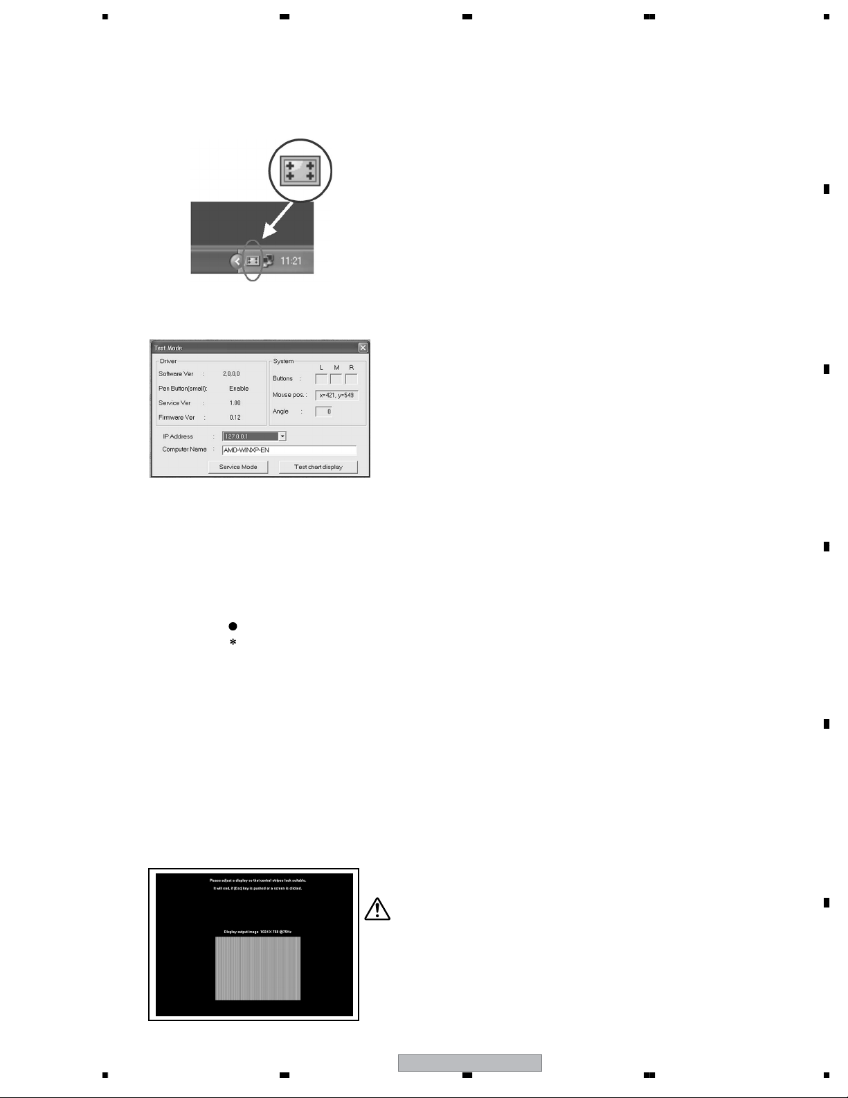
5678
7. GENERAL INFORMATION
7.1 DIAGNOSIS
7.1.1 TEST MODE
This is a service mode. Click “Test Mode” under “Hardware Information” in the CBdrvU task tray to open the screen shown
below.
Click left → Hardware Information → Test Mode
a) State display
This screen shows results of hardware checks and the state of the driver and the operating system (Windows).
A
B
[Function overview]
• Driver
Software Ver : Indicate the version of the CBdrvU setup program
Pen Button (small) : Indicate the setting of the small pen button in the Property screen
Service Ver : Indicate the version of the USB filter driver
Firmware Ver : Indicate the version of the handwriting device firmware
• System
Buttons : : Correctly recognized
: Not correctly recognized (during 3-button mouse emulation)
L: Left mouse button
R: Right mouse button
M: Middle mouse button
Mouse pos : Indicate mouse coordinates recognized by Windows
Angle : Indicate currently set rotate angle
IP Address : Indicate IP address of the connected PC
Computer Name : Indicate the name of the connected PC
Service Mode : Indicate handwriting device service information and DIP switch information.
This mode is not required during normal operation.
Test chart display : Adjust plasma display. This mode is not required for normal operation.
b) Test chart display
This is a service mode. Use it to adjust plasma display settings.
C
D
E
Notes:
• The plasma display need not be adjusted if it has already been set up.
• Use the supplied remote control to adjust the plasma display.
For details, refer to the Operating Instructions.
• Press the [Esc] key or use the pen to click on the screen.
PDK-50HW3
56
F
87
7
8
Page 88

1234
7.1.2 SELF TEST FUNCTION (SelfTest)
A self-test for the optical system of the Handwriting System can be performed.
A
Service Mode
Press the [Service Mode] button in the “Test Mode” screen to open the “Service Information” screen.
a) Screen items
This screen shows service information and DIP switch information for handwriting device.
B
[Displayed service information]
LED/Sens Area :Test board number (refer to the PDK-50HW3 service manual.)
C
Point :Test address number
Status :Assessment Normal = OK
Malfunction = E01, ALL, Check
[Displayed DIP SW information]
Handwriting device DIP switch information (Binary expression)
[SelfTest button]
Perform self test. The button cannot be pressed using the touch screen. Click the button using the mouse withouttouching the
screen. Do not touch the screen until screen changes on the next item b) appears.
b) Status displayed after pressing SelfTest button
D
1. When LED and Sens are normal
The detailed list (in the lower half of screen) shows no data.
Relationship between Area and board location isshown below.
Sens boards
HI J K
N
E
LED
boards
M
L
FRONT SIDE VIEW
G
Sens
F
boards
E
AB CD
LED boards
F
88
1234
PDK-50HW3
Page 89

5678
2. When all components of test board D (LED) and all components of test board K (Sens) are malfunctioning.
The detailed list indicates “ALL” and not data for each Point.
Note:
“ALL” may indicate a malfunction that is not caused by the specific board.
Control signal lines from the test board A (LED) and optical signals lines
to the test board A (LED) are relayed via other boards so a malfunction
could be caused by defective connectors on boards in this chain.
3. When some components of test board A (LED) and all test board H (Sens) components are malfunctioning “Check” is
indicated when some components are malfunctioning.
The test address number and assessment for all related LED and Sens appear in the detailed list.
A
B
Note:
Execute a self-test only in Normal mode. Correct test results may not be obtained in Low Scan Lock mode or Super Low Scan Lock mode.
See the "DIP SW Information" display to check that the second and fourth switches from the left are set to 0. The "DIP SW Information"
display shows the status of the DIP switches on the LED-A assy.
If a change of the settings is required, first disconnect the USB connector between the Handwriting System and the plasma display, because
resetting of the Handwriting device is required, then change the settings. Then reconnect the Handwriting System to the plasma display.
If the Handwriting System is not connected to the plasma display, correct test results will not be obtained.
When the PC starts up or a USB cable is connected, the message
indicated on the right will appear.
The power indicator will flash alternately in green and orange.
As optical checking is being performed while the indicator is flashing,
do NOT touch the screen. Also do NOT touch the screen while a
self-test is being performed.
Now Setting...
Please do not touch the screen.
C
D
E
56
PDK-50HW3
F
89
7
8
Page 90
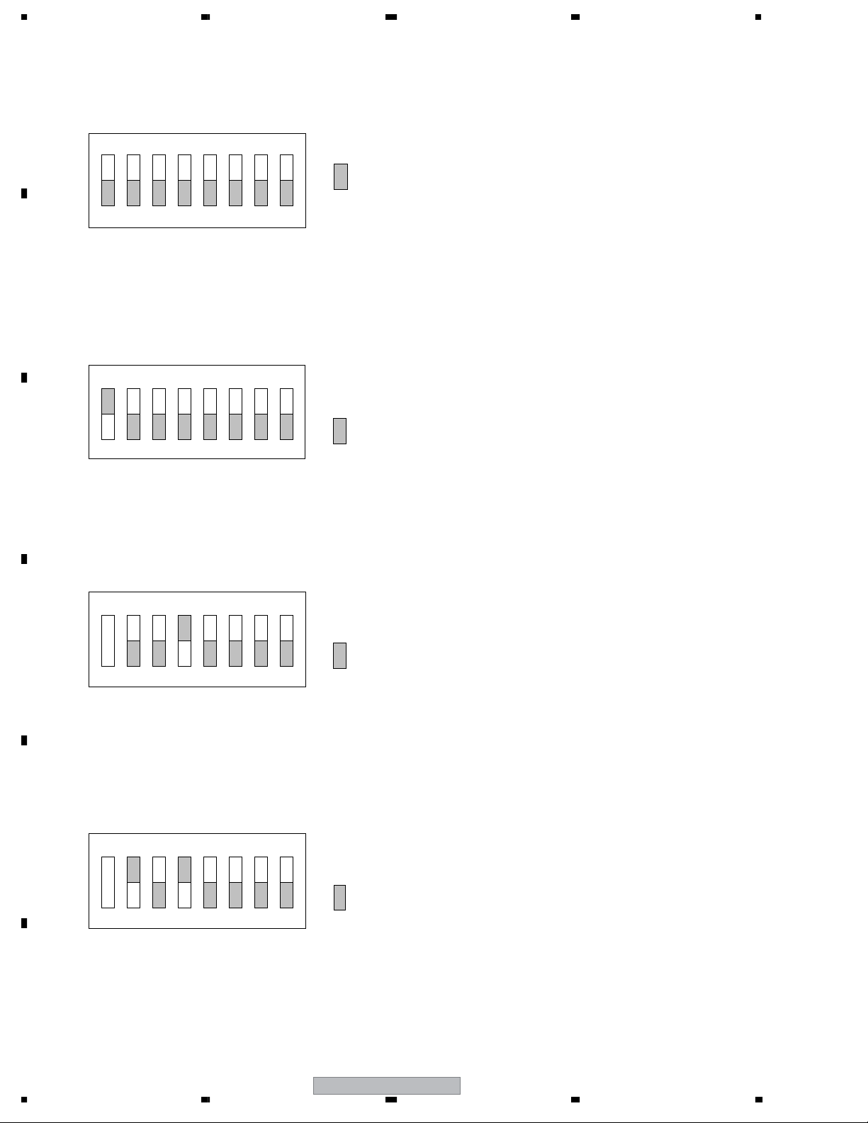
1234
7.1.3 INTERNAL DIP SWITCH SETTINGS
The test board A (LED) in the device is provided with 8-bit DIP switches (SW1).
DIP switch settings are read only when the device is powered up and their values stay the same.
A
Factory default status
ON
: Factory default setting
(All off)
1234 5678
* Bits 5 to 8 should always be set to OFF.
The following operations can be performed by changing DIP switch settings as shown below.
B
a) To lock device in the NORMAL mode
This setting overrides the mode selector switch [PEN] or [NORMAL] on the rear panel of the device and locks it in
NORMAL mode.
ON
: Set side
1234 5678
C
b) To make waveform observations (Low Scan Lock mode)
¶ This setting locks the device in low scan mode (all scan) suitable for waveform observation using an oscilloscope.
¶ The touch panel input functions do not operate in this mode.
¶ The power indicator on the device front panel blink continuously in approximately 0.5 second cycles.
ON
D
12345678
c) To make observations of infrared LED light emitting status using a CCD camera (Super Low Scan Lock mode)
¶ This setting performs a slow scan in approximately 1 second cycles.
¶ The light emitting status of infrared LEDs can be observed in a dark room, but this depends on the camera used.
¶ The touch panel input functions do not operate in this mode.
¶ The power indicator on the device front panel blinks continuously in approximately 1 second cycles.
E
: Set side
Bits that are not indicated can be set to any value.
ON
: Set side
12345678
F
90
1234
Bits that are not indicated can be set to any value.
PDK-50HW3
Page 91

5678
7.1.4 OPERATION CHECKS USING EXCHANGEABLE ASSY'S
As some Assy's become exchangeable by changing their jumper-pin settings, in some cases, operation checks of the Assy in
an area in failure are possible if you use an Assy in an area without problems.
• LED Assy's
On the LED-B and LED-C Assy's, the dedicated control lines for the LED-B and LED-C are determined by jumper-pin
settings (positions to which 0-ohm resistors are inserted).
By changing jumper-pin settings on these Assy's, you can use the LED-B Assy as the LED-C Assy, and vice versa.
Assy/JP JP1 JP2 JP3
LED-B ? ××
LED-C × ? ×
Note: ?: With a 0-ohm resistor attached to the jumper pin, ×: Without a 0-ohm resistor attached
• With a resistor attached to JP1, the Assy is connected to the control line for HBOARD_SEL (1).
• With a resistor attached to JP2, the Assy is connected to the control line for HBOARD_SEL (2).
• Do NOT make a connection to JP3.
The following Assy's for the LEDs are dedicated, and they are not exchangeable by changing JP settings.
LED-A −−LED-D
LED-E LED-F LED-G
A
B
• SENSOR Assy's
On the SENSOR-I, SENSOR-J, and SENSOR-K Assy's, the sensor signal lines and the dedicated control lines for
SENSOR-I, SENSOR-J, and SENSOR-K are determined by jumper-pin settings (positions to which 0-ohm resistors are
inserted).
By changing jumper-pin settings on these Assy's, you can use the SENSOR-I, -J, and -K Assy's one in place of another.
It should be noted, however, that the SENSOR-K Assy needs a connector for servicing (Service Part No.: BZK1517)
attached, as the CN1 (40-pin) connector is not provided with this Assy.
Assy/JP JP1 & JP5 JP2 & JP6 JP3 & JP7 JP4 & JP8
SEN-I ? ×××
SEN-J × ? ××
SEN-K ××? ×
Note: ?: With a 0-ohm resistor attached to the jumper pin, ×: Without a 0-ohm resistor attached
• With a resistor attached to JP1, the Assy is connected to the control line for HSDEC_SEL (1), and with a resistor
attached to JP5, the Assy is connected to the sensor-signal line for H_RCV (I).
• With a resistor attached to JP2, the Assy is connected to the control line for HSDEC_SEL (2), and with a resistor
attached to JP6, the Assy is connected to the sensor-signal line for H_RCV (J).
• With a resistor attached to JP3, the Assy is connected to the control line for HSDEC_SEL (3), and with a resistor
attached to JP7, the Assy is connected to the sensor-signal line for H_RCV (K).
• JP1 and JP5, JP2 and JP6, and JP3 and JP7 must be set in pairs.
• Do NOT make any connections to JP4 or JP8.
The following Assy's for the SENSORs are dedicated, and they are not exchangeable by changing JP settings.
SEN-H −−−
SEN-L SEN-M SEN-N
C
D
E
56
PDK-50HW3
F
91
7
8
Page 92

1234
8. PANEL FACILITIES
A
Main Unit
B
IR transmitting filter
PEN
NORMAL
Rear side
of unit
Mode selector switch
Set the mode switch in
accordance with whether
you will use the special
pen or other device to
input characters and lines
on the screen.
PEN Mode:
In this mode, the
special accessory
pen can be used to write
on the screen. Using the
special pen allows the
drawing of more clearly
delineated characters and
lines.
NORMAL Mode:
In this mode, your
finger or other
object can be used to write
on the screen. This mode
will produce lower screen
definition, however,
compared to drawing with
the dedicated input pen.
NOTE:
C
Pen
D
Power indicator
(Lights green when ON)
Holes in rear end of pen
LED indicator
Tip
Cap
When the power switch is first turned on, the power indicator will
flash orange; while the indicator is flashing, do not touch the
screen, since the unit is initializing its internal settings.
If pen operation becomes difficult:
The pen may fail to operate properly if the holes in
rear end of pen are blocked. Also, the pen may
begin operating erratically when the battery
becomes depleted. In this event, change the
battery at your earliest opportunity.
Battery cover
Confirming Battery Life:
Large button
(corresponds to right
mouse button)
E
Small button
(The function corresponding to middle
When the small button is depressed fully, an LED
indicator will light. If the indicator fails to light, or
lights only dimly, the battery is depleted and
should be replaced.
mouse button can be assigned using
the driver software.)
Pen tip
(corresponds to left mouse button)
F
92
1234
PDK-50HW3
 Loading...