

Page 1
DUAL DRIVE AMPLIFIER
M-AX10
THIS MANUAL IS APPLICABLE TO THE FOLLOWING MODEL(S) AND TYPE(S).
Type
KU/CA AC120V
NY AC230V
Model
M-AX10
Power Requirement Remarks
ORDER NO.
RRV2345
CONTENTS
1. SAFETY INFORMATION
2. EXPLODED VIEWS AND PARTS LIST
3. SCHEMATIC DIAGRAM
4. PCB CONNECTION DIAGRAM
5. PCB PARTS LIST
6. ADJUSTMENT
PIONEER CORPORATION 4-1, Meguro 1-chome, Meguro-ku, Tokyo 153-8654, Japan
PIONEER ELECTRONICS SERVICE, INC. P.O. Box 1760, Long Beach, CA 90801-1760, U.S.A.
PIONEER EUROPE NV Haven 1087, Keetberglaan 1, 9120 Melsele, Belgium
PIONEER ELECTRONICS ASIACENTRE PTE. LTD. 253 Alexandra Road, #04-01, Singapore 159936
c
PIONEER CORPORATION 2000
...............................................
....................................................
......................................
................
.....................................
..........................
12
24
36
41
2
3
7. GENERAL INFORMATION
7.1 IC
7.2 PROTECTION CIRCUIT
7.3 EXPLANATION
8. PANEL FACILITIES AND SPECIFICATIONS
.................................................................
7.3.1 PRODUCT OVERVIEW
7.3.2 CIRCUIT DESCRIPTION
................................
.............................
............................................
.......................
.....................
T – ZZV JULY. 2000 Printed in Japan
....
42
42
52
54
54
55
58
Page 2
M-AX10
1. SAFETY INFORMATION
This service manual is intended for qualified service technicians ; it is not meant for the casual do-ityourselfer. Qualified technicians have the necessary test equipment and tools, and have been trained
to properly and safely repair complex products such as those covered by this manual.
Improperly performed repairs can adversely affect the safety and reliability of the product and may
void the warranty. If you are not qualified to perform the repair of this product properly and safely, you
should not risk trying to do so and refer the repair to a qualified service technician.
WARNING
This product contains lead in solder and certain electrical parts contain chemicals which are known to the state of California to cause
cancer, birth defects or other reproductive harm.
Health & Safety Code Section 25249.6 – Proposition 65
NOTICE
(FOR CANADIAN MODEL ONLY)
Fuse symbols (fast operating fuse) and/or (slow operating fuse) on PCB indicate that replacement parts must
be of identical designation.
REMARQUE
(POUR MODÈLE CANADIEN SEULEMENT)
Les symboles de fusible (fusible de type rapide) et/ou (fusible de type lent) sur CCI indiquent que les pièces
de remplacement doivent avoir la même désignation.
(FOR USA MODEL ONLY)
1. SAFETY PRECAUTIONS
The following check should be performed for the
continued protection of the customer and service
technician.
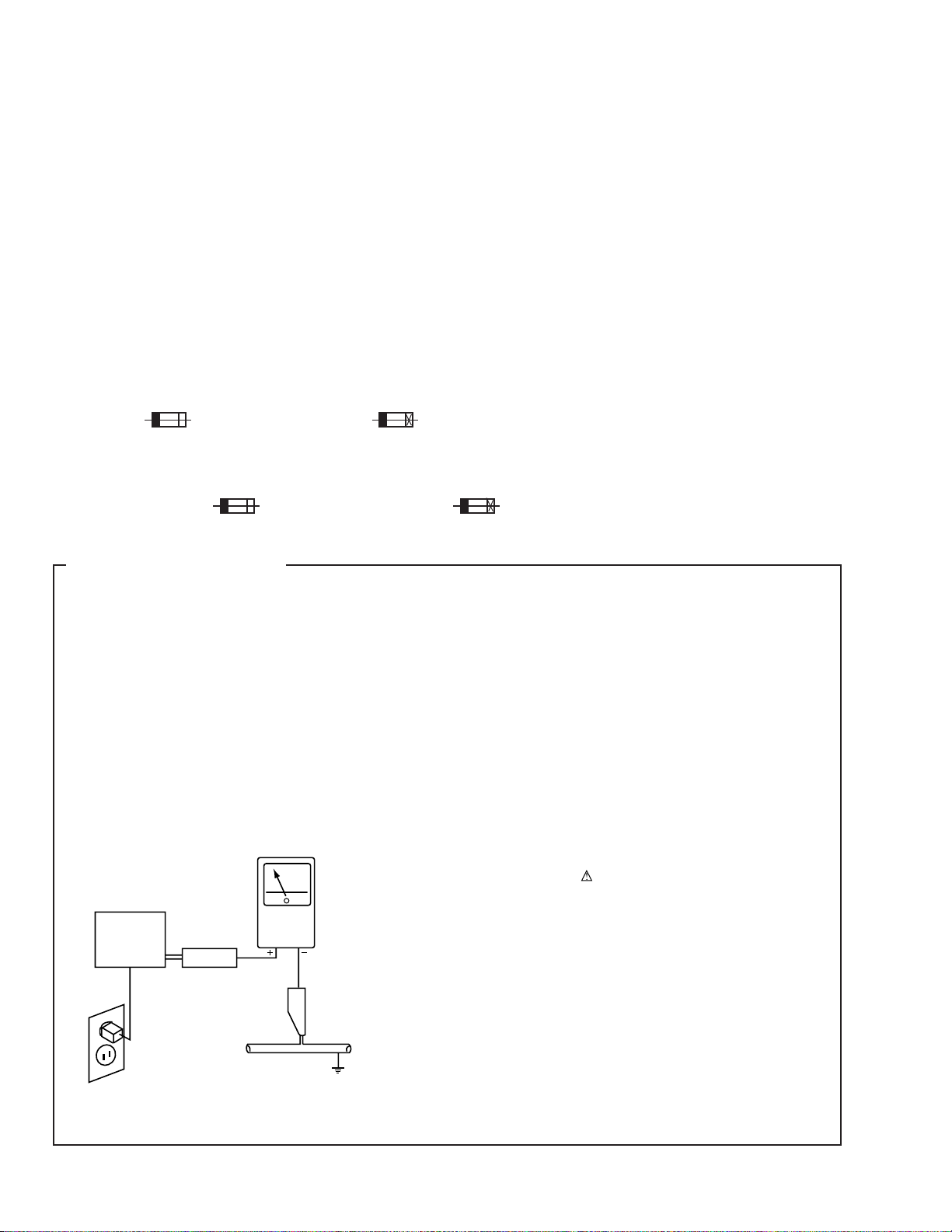
LEAKAGE CURRENT CHECK
Measure leakage current to a known earth ground (water
pipe, conduit, etc.) by connecting a leakage current tester
such as Simpson Model 229-2 or equivalent between the
earth ground and all exposed metal parts of the appliance
(input/output terminals, screwheads, metal overlays, control
shaft, etc.). Plug the AC line cord of the appliance directly
into a 120V AC 60Hz outlet and turn the AC power switch
on. Any current measured must not exceed 0.5mA.
Reading should
not be above
0.5mA
Earth
ground
Device
under
test
Also test with
plug reversed
(Using AC adapter
plug as required)
Leakage
current
tester
Test all
exposed metal
surfaces
ANY MEASUREMENTS NOT WITHIN THE LIMITS
OUTLINED ABOVE ARE INDICATIVE OF A POTENTIAL
SHOCK HAZARD AND MUST BE CORRECTED BEFORE
RETURNING THE APPLIANCE TO THE CUSTOMER.
2. PRODUCT SAFETY NOTICE
Many electrical and mechanical parts in the appliance
have special safety related characteristics. These are
often not evident from visual inspection nor the protection
afforded by them necessarily can be obtained by using
replacement components rated for voltage, wattage, etc.
Replacement parts which have these special safety
characteristics are identified in this Service Manual.
Electrical components having such features are identified
by marking with a
in this Service Manual.
The use of a substitute replacement component which does
not have the same safety characteristics as the PIONEER
recommended replacement one, shown in the parts list in
this Service Manual, may create shock, fire, or other hazards.
Product Safety is continuously under review and new
instructions are issued from time to time. For the latest
information, always consult the current PIONEER Service
Manual. A subscription to, or additional copies of, PIONEER
Service Manual may be obtained at a nominal charge from
PIONEER.
on the schematics and on the parts list
AC Leakage Test
2
Page 3
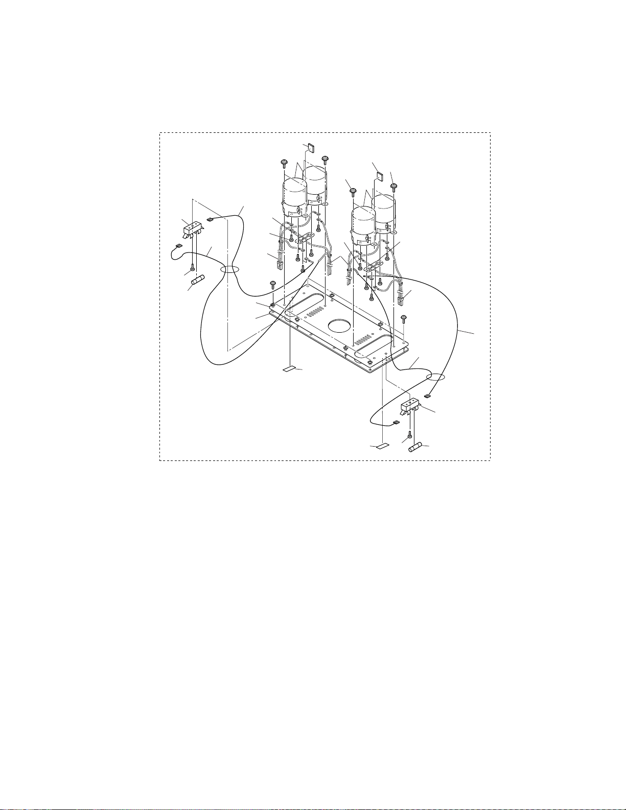
2. EXPLODED VIEWS AND PARTS LIST
NOTES:• Parts marked by "NSP" are generally unavailable because they are not in our Master Spare Parts List.
2.1 PACKING
The mark found on some component parts indicates the importance of the safety factor of the part.
•
Therefore, when replacing, be sure to use parts of identical designation.
Screws adjacent to mark on the product are used for disassembly.
•
1
3
M-AX10
4
5
10
9
6
FRONT
7
11
2
(1) PACKING PARTS LIST
Mark No. Description Part No.
NSP 1 Literature Bag AHG-117
2 Instruction Manual (E) ARB7217
NSP 3 Warranty Card See Contrast table (2)
NSP 4 Warranty Card See Contrast table (2)
5 Styrol Protector L AHA9014
6 Styrol Protector R AHA9015
7 Packing Case See Contrast table (2)
8 Door Sheet AHG7064
9 Mirror Mat RHC1024
10 Polyester Bag VHL1004
11 Recycle Label See Contrast table (2)
8
(2) CONTRAST TABLE
M-AX10/KU/CA and M-AX10/NY are constructed the same except for the following:
Mark
No.
NSP 3 Warranty Card ARY7045 Not used
NSP 4 Warranty Card Not used ARY7022
7 Packing Case AHD7875 AHD7874
11 Recycle Label ARW7091 Not used
Symbol and Description
M-AX10/KU/CA M-AX10/NY
Part No.
Remarks
3
Page 4
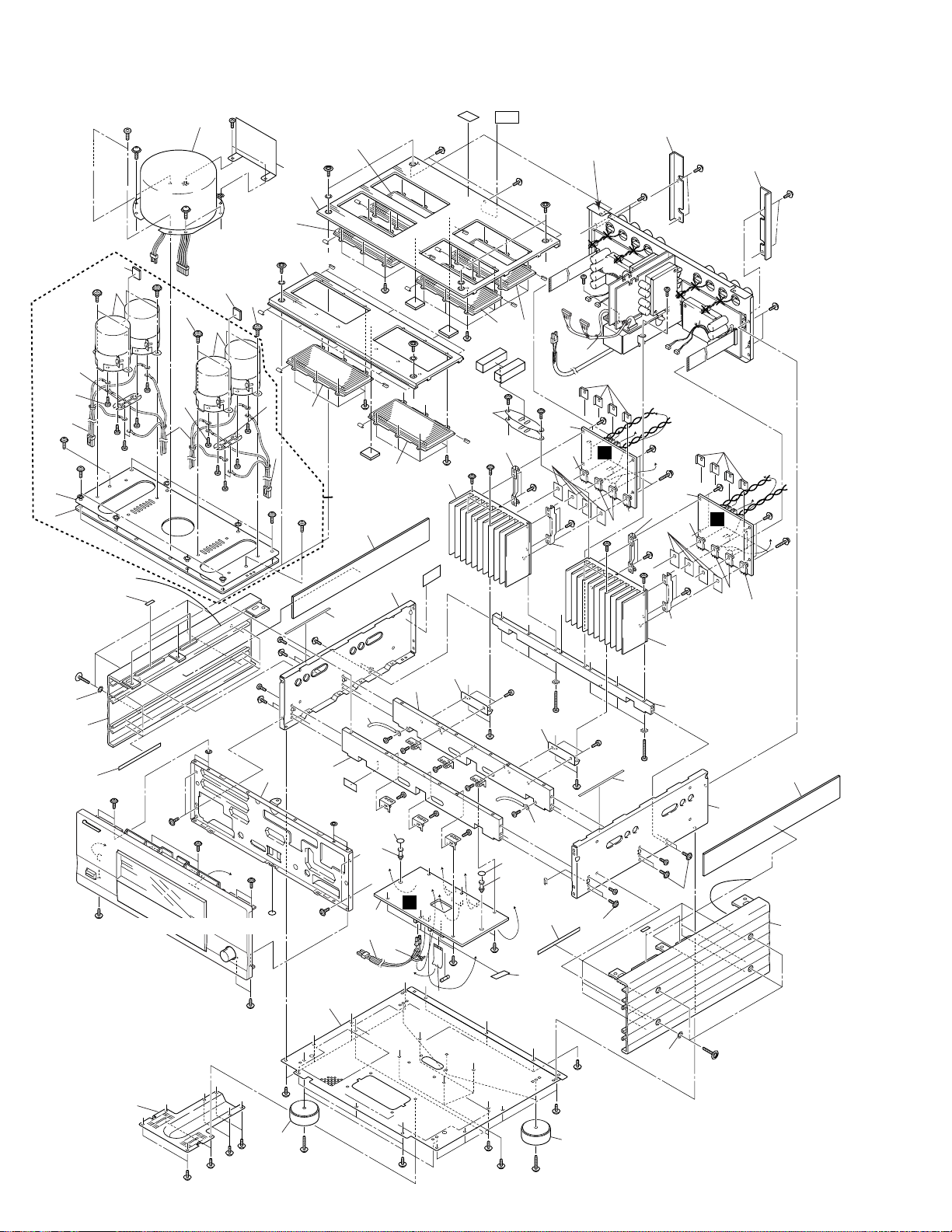
M-AX10
2.2 EXTERIOR
64
32
52
6
25
71
11
83
27
60
Take care to the edge
when sevicing
73
64
73
47
71
C
73
38
53
37
42
G
44
Refer to "2.4 FRONT PANEL"
46
52
71
77
71
49
39
90
68
39
39
39
73
34
34
67
73
39
67
78
26
88
24
16
70
62
70
62
62
62
70
A
62
70
N
O
B
B
P
Q
67
8
9
7
64
57
11
64
57
79
56
39
55
57
83
42
49
73
39
36
67
39
34
for NY type
37
45
16
85
40
G
21
33
30
10
62
50
67
39
57
19
62
70
35
D
3
75
73
73
77
32
44
49
73
52
36
39
25
71
71
F
73
61
45
61
45
20
Q
42
51
A
B
52
6
71
75
71
D
73
E
46
73
73
40
42
42
89
Refer to "2.3 REAR PANEL"
45
49
39
72
31
91
57
N
P
76
1
15
44
74
48
24
30
36
37
39
57
31
76
14
22
78
76
70
62
35
50
E
67
44
22
62
59
58
45
42
H
I
62
4
37
38
J
K
M
H
C
I
I
78
44
22
L
74
48
67
43
15
22
26
17
61
2
44
45
23
67
J
4
L
5
18
Take care to the edge
L
O
75
23
67
H
4
I
5
78
72
76
61
45
45
42
J
F
K
K
67
43
M
4
33
when servicing
54
44
44
28
29
68
80
68
4
45
65
44
69
80
44
29
65
73
47
Page 5
82
12
for KU type
32
52
6
25
52
52
M-AX10
32
52
6
83
81
12
75
27
60
11
71
73
64
71
71
71
75
71
46
C
73
86
71
D
73
E
46
73
73
87
73
71
71
83
25
11
F
64
12
12
75
82
81
5
Page 6

M-AX10
(1) EXTERIOR PARTS LIST
Mark No. Description Part No.
1 C.AMP (L) ASSY See Contrast table (2)
2 C.AMP (R) ASSY See Contrast table (2)
3 POWER SUPPLY ASSY See Contrast table (2)
4 Power MOS FET IRFP140
(Q1,Q2,Q5,Q6)
5 Power MOS FET IRFP9140
(Q3,Q4,Q7,Q8)
6 Electric Capacitor(C1-C4) ACH7156
7 Power Transformer See Contrast table (2)
8 Fuse (FU1) See Contrast table (2)
9 16P FFC 60V (J17) ADD7155
10 Wire with 2P Housing (J18) ADX7336
11 Cable (J9,J10) ADX7337
NSP 12 Cable (J23,J24) See Contrast table (2)
13 • • • • • • • • • •
14 PCB Holder (PLS) AEC7316
15 Plate AEE7030
16 Stay L (MET) ANA9006
17 Stay S (MET) ANA9007
18 Side Frame R ANA9008
19 Side Frame L ANA9009
20 Panel Stay (MET) AND7033
NSP 21 Bottom Plate ANF7012
22 PCB Holder ANG1474
23 Transistor Cover L ANG1724
24 L Type Plate ANG7248
25 Earth Plate ANG9102
NSP 26 Heat Sink (AL) ANH7105
27 Sub Inner Plate (MET) ANK7080
28 AC Code Cover (MET) ANK9024
29 Insulator ANL7012
30 Cord Clamper RNH-184
NSP 31 Spacer AEB7168
NSP 32 Spacer AEB7170
NSP 33 Damping Plate AMR7280
NSP 34 Damping Plate AMR7281
35 Cushion A PED1001
NSP 36 Sheet PED1006
NSP 37 Tape PNM-045
NSP 38 Tape PNM1160
NSP 39 Tape PNM1249
NSP 40 Washer (Plastic) RBF-085
41 • • • • • • • • • •
42 Screw ABA1011
43 Screw ABA1082
44 Screw (Steel) ABA1192
45 Screw (Steel) ABA1193
Mark No. Description Part No.
46 Screw (Steel) ABA1207
47 Screw (Steel) ABA7006
48 Screw (Steel) ABA7045
49 M4 SH Screw ABA7051
50 PCB Spacer (3 × 12) AEC1372
51 Washer (PVC) RBF1034
52 Screw VBA1056
53 Side AL L AAH7033
54 Side AL R AAH7034
55 Top Plate F (AL) AAH7035
56 Top Plate R (AL) AAH7036
57 Bonnet Escutcheon AAK7658
58 Rear Mole R AAP7056
59 Rear Mole L AAP7057
60 Innner Plate (MET) ANK7081
61 Screw BBT30P100FCC
62 Screw BBT30P080FCC
63 • • • • • • • • • •
64 Screw IBZ40P140FCC
65 Screw BBZ40P180FCC
66 • • • • • • • • • •
67 Screw IBZ30P060FCC
68 Screw IBZ30P080FCC
69 Screw IBZ40P080FCC
70 PCB Holder (MET) ANG9101
71 Screw PMZ40P060FCU
72 Screw VBZ35P080FMC
73 Washer (CU) WG40FCC
74 Washer WH30FUC
75 Binder ZCA-SKB90BK
76 Screw ABA1050
77 Screw IBZ40P080FCC
78 Screw ABA1208
79 Trans Shield ANK7074
80 Screw VCZ30P100FMC
81 Fuse (FU2,FU3) See Contrast table (2)
82 Fuse Holder See Contrast table (2)
83 Screw BBZ40P080FCC
84 UL Caution Card AAX-313
NSP 85 IPC Caution Label See Contrast table (2)
NSP 86 Fuse Card See Contrast table (2)
NSP 87 Fuse Card See Contrast table (2)
NSP 88 Micro Fuse Caution Card See Contrast table (2)
89 65 Label See Contrast table (2)
NSP 90 FCC Label See Contrast table (2)
NSP 91 Fuse Card See Contrast table (2)
Refer to next page about Contrast table (2).
6
Page 7
(2) CONTRAST TABLE
M-AX10/KU/CA and M-AX10/NY are constructed the same except for the following:
M-AX10
Mark
No.
Symbol and Description
Part No.
M-AX10/KU/CA M-AX10/NY
1 C. AMP(L) ASSY AWX7673 AWX7280
2 C. AMP(R) ASSY AWX7674 AWX7281
3 POWER SUPPLY ASSY AWX7664 AWX7662
7 Power Transformer ATS7277 ATS7251
8 Fuse (FU1) VEK1029 REK-106
(10A) (4A)
NSP 12 Cable (J23,J24) ADX7335 Not used
81 Fuse (FU2,FU3) AEK7069 Not used
(20A)
82 Fuse Holder AKR7002 Not used
NSP 85 IPC Caution Label AAX7784 Not used
NSP 86 Fuse Card AAX7795 Not used
NSP 87 Fuse Card AAX7796 Not used
NSP 88 Micro Fuse Caution Label AAX7810 Not used
89 65 Label ARW7050 Not used
NSP 90 FCC Label VRW1559 Not used
NSP 91 Fuse Card Not used AAX1589
Remarks
7
Page 8
M-AX10
2.3 REAR PANEL
3 or 4
G
26
I
27
13
14
33
22
20
35
46
B
A
30
27
E
32
31 31
36
34
E
G
19
11
F
H
46
40
21
29
8
7
28
43
13
44
28
8
37
8
10
28
42
47
24
41
16
38
28
38
28
6
8
7
37
32
17
38
15
24
11
C
H
38
9
18
18
A
18
38
B
38
D
C
D
38
9
28
39
18
10
26
25
A
G
22
F
5
30
23
45
26
27
H
K
1 or 2
32
21
25
26
27
40
8
Page 9

REAR PANEL PARTS LIST
(1)
Mark No. Description Part No.
1 V.AMP (L) ASSY AWX7278
2 V.AMP (R) ASSY AWX7279
3 INPUT (L) ASSY AWX7273
NSP 5 JOINT ASSY AWX7283
10 AC Cord with Plug See contrast tabel (2)
4 INPUT (R) ASSY AWX7274
6 Ground Terminal AKE-046
7 Speaker Terminal 1P AKE7009
(CN1,CN2,CN5,CN6)
8 Speaker Terminal 1P AKE7010
(CN3,CN4,CN7,CN8)
9 23P FFC 60V (J5,J6) ADD7154
11 11P Housing Wire (J3,J4) ADX7278
12 • • • • • • • • • •
13 Connector Assy (J7) PG10MM-F15
14 Connector Assy (J8) PG10MM2F15
15 Rear Panel (MET) ANC7820
16 Rear Panel Plate R See contrast tabel (2)
17 Rear Panel Plate L See contrast tabel (2)
18 PCB Holder (MET) ANG9101
19 Shield Plate(PLS) ANK7076
20 AC Shield L ANK9025
M-AX10
NSP 22 Spacer AEB7169
NSP 23 Tape AEH7008
NSP 24 Damping Plate AMR7278
NSP 25 Damping Plate AMR7281
NSP 26 Tape PNM1249
NSP 33 PCB Spacer (14) DEC1387
NSP 46 Earth Lead Wire DE025BF0
21 Shield Cover ANK9026
27 Fiber Washer RBF1045
28 Screw ABA1192
29 Screw BBT30P100FCC
30 Screw ABA1207
31 Rivet AEC-441
32 Nylon Rivet AEC7242
34 Card Spacer DEC1772
35 PC Support VEC1549
36 Cushion A PED1001
37 Screw BBZ30P080FCC
38 Screw IBZ30P060FCC
39 Nut NK70FCU
40 Binder ZCA-SKB90BK
41 Input Plate (MET) ANG7274
42 Locking Card Spacer VEC1596
43 Ferrite Core See contrast tabel (2
44 Screw ABA1011
45 AC Shield Case (PLS) ANK7075
47 AC Cord Spacer ANG1153
(2) CONTRAST TABLE
M-AX10/KU/CA and M-AX10/NY are constructed the same except for the following:
Mark
No.
Symbol and Description
M-AX10/KU/CA M-AX10/NY
10 AC Cord with Plug ADG7041 ADG7038
16 Rear Panel Plate R ANC7288 ANC7285
17 Rear Panel Plate L ANC7289 ANC7286
43 Ferrite Core Not used ATX1031
Part No.
Remarks
9
Page 10
M-AX10
2.4 FRONT PANEL
40
36
35
34
42
14
46
17
11
44
23
26
18
15
38(2/3)
20
C
38(1/3)
24
10
19
42
49
44
25
16
1
21
32
22
44
12
47
43
6
43
7
44
44
5
41
3
39
31
13
D
44
44
27
29
41
12
47
9
49
10
42
E
4
8
27
29
10
30
44
28
44
43
33
48
44
45
44
38(3/3)
F
2
42
37
Page 11

FRONT PANEL PARTS LIST
•
Mark No. Description Part No.
NSP 1 SW ASSY AWX7282
NSP 2 VR ASSY AWX7334
NSP 4 LED ASSY AWX7277
NSP 5 Cord with Plug ADH7022
3 FRONT ASSY AWX7276
M-AX10
NSP 6 Cord with Plug (J20) DE005VF0
NSP 13 Spacer AEB7169
NSP 14 Damping Plate AMR7282
NSP 15 Tape PNM1249
NSP 16 Cushion A REB1060
NSP 17 Cushion B REB1061
7 Magnet AMF7003
8 Door Hinji L (PLS) AMR9199
9 Door Hinji R (PLS) AMR9200
10 Door Assy (MET) ANG9100
11 Inner Panel (AL) ANB7184
12 Damper Assy AXA9013
18 LED Lens AAK2459
19 LED Filter S(PLS) AAK7657
20 LED Film (PLS) AAK7669
21 Display Panel L (PLS) AAK9044
22 Cover AAK9045
23 LED Filter L (PLS) AAK9046
24 Mode Panel (PLS) AAK9047
25 Mode Lens (PLS) AAK9048
26 Panel S (PLS) AAK9049
27 Door Cushion AED9014
28 Tape AEH7009
29 Door Yoke (MET) ANB7187
30 Name Plate G (AL) PAN1377
31 Cushion A PED1001
32 Knob S (PLS) AAB7200
33 Knob M (AL) AAB7201
34 Block ANL7015
35 Power Button (ABS) VNK4159
36 Side Panel L (AL) AAH7037
37 Side Panel R (AL) AAH7038
38 Panel Base (PLS) AMB9020
39 Door Panel (AL) ANB7182
40 Front Panel (AL) ANB7183
41 Screw BBT30P080FCC
42 Screw BBZ30P080FCC
43 Screw IBZ30P060FCC
44 Screw IBZ30P080FCC
45 Nut NK90FCU
46 Screw PMH30P060FMC
47 Screw PSZ20P060FMC
48 Screw (STEEL) ABA1050
49 Washer (PLS) ABF7007
11
Page 12
1
23
M-AX10
3. BLOCK DIAGRAM AND SCHEMATIC DIAGRAM
3.1 OVERALL CONNECTION DIAGRAM AND JOINT ASSY
4
A
E
LED ASSY (AWX7277)
FRONT ASSY
D
(AWX7276)
F
VR ASSY
(AWX7334)
B
POWER SUPPLY ASSY
KU/CA : (AWX7664)
NY : (AWX7662)
B
L712 RTF1167
R712 2.2
I
C.AMP(L) ASSY
KU/CA : (AWX7673)
NY : (AWX7280)
C
L711
RTF1167
G
H
V.AMP(L) ASSY
(AWX7278)
D
INPUT(L) ASSY
(AWX7273)
12
A
1234
Page 13

5
C
SW ASSY
(AWX7282)
678
M-AX10
Note : When ordering service parts, be sure to refer to "EXPLODED VIEWS
and P AR TS LIST" or "PCB PAR TS LIST".
A
B
From
AC Power Cord
A
JOINT ASSY
(AWX7283)
J
INPUT(R) ASSY
(AWX7274)
L
C.AMP(R) ASSY
KU/CA : (AWX7674)
NY : (AWX7281)
C
K
V.AMP(R) ASSY
(AWX7279)
D
A
5
6
7
8
13
Page 14
A
1
23
M-AX10
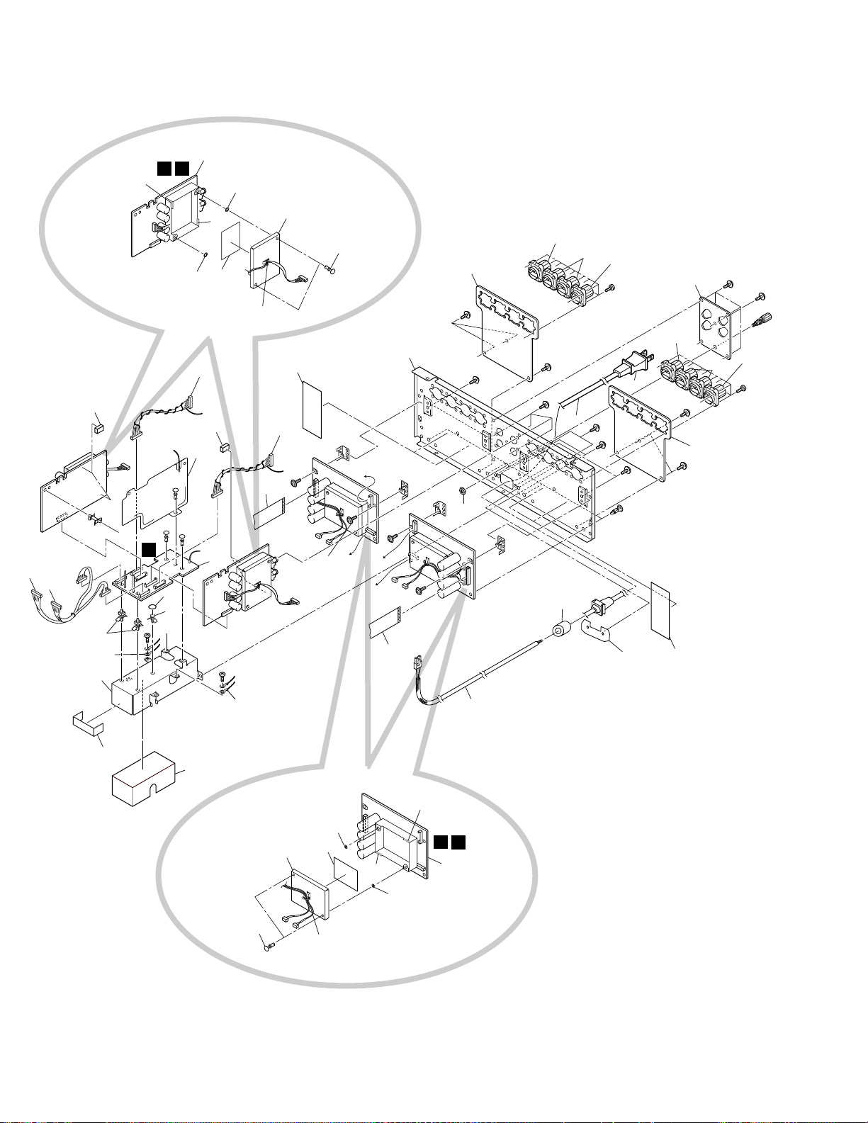
3.2 POWER SUPPLY, SW ASSY
4
B
POWER SUPPLY ASSY
(KU/CX :AWX7664 ,NY :AWX7662)
C1, C3
J805
and
J801
CN803
6
5
4
3
1
J803
I
CN501
PIOWER TRANSFORMER
120V(KU/CA)
230V (/NY)
B
6
5
1
22
4
3
C2, C4
and
K
CN601
C
J802
J804
J808
J806
C
SW ASSY
(AWX7282)
CN701
D
CN853
CN852
CN851
FU1
FU1
KU :VEK1029(10A)
NY :REK-106(4A)
14
B C
1234
Page 15
5
678
M-AX10
A
CN711
CN805
A
CN804
D
CN901
B
+24V
+24V
C
CN806
• NOTE FOR FUSE REPLACEMENT
CAUTION -
5
FOR CONTINUED PROTECTION AGAINST RISK OF FIRE.
REPLACE WITH SAME TYPE AND RATINGS ONLY.
6
A
CN712
D
B
7
8
15
Page 16
1
M-AX10
3.3 FRONT, LED, VR ASSY
A
CN901
B
CN804
B
23
4
C
E
LED ASSY
(AWX7277)
D
16
CN751
J902
CN761
J901
VR ASSY
F
(AWX7334)
D E F
1234
Page 17

5
678
M-AX10
FRONT ASSY
D
(AWX7276)
SWITCHES
S901 : ATT THROUGH
S902 : ATT HOLD
S903 : INPUT
S904 : ILLUMINATION
S905 : MODE
A
B
C
D
D
5
6
7
8
17
Page 18
1
M-AX10
3.4 INPUT (L), INPUT (R) ASSY
A
INPUT(L) ASSY
G
(AWX7273)
B
23
12dB FLAT AMP
4
JA101
C
JA102
D
18
G
1234
Page 19

5
678
M-AX10
J201
K
CN401
A
JA201
JA202
INPUT(R) ASSY
J
(AWX7274)
CN201
A
CN714
SIGNAL ROUTE
: AUDIO SIGNAL
B
DAC VR
J101
CN101
H
CN301
A
CN713
C
D
G
5
6
7
J
8
19
Page 20

1
M-AX10
3.5 V.AMP (L) ,V.AMP (R) ASSY
A
B
23
V. AMP(L) ASSY
H
(AWX7278)
4
14dB POWER AMP
J101
C
G
DC ADJ(HL)
CN301
CN302
A
CN715
DC ADJ(LL)
D
20
H
1234
Page 21

5
678
M-AX10
SIGNAL ROUTE
: AUDIO SIGNAL
J401
A
J301
L
CN607
J302
I
CN507
I
CN508
I
CN502
J
J201
CN401
CN402
J402
V. AMP(R) ASSY
(AWX7279)
K
L
CN608
B
L
CN602
CN403
C
A
CN303
J306
5
6
CN716
7
H
K
8
D
21
Page 22

1
M-AX10
3.6 C.AMP (L), C.AMP (R) ASSY
A
CN505
B
23
C. AMP(L) ASSY
I
(KU/CA : AWX7673)
( NY : AWX7280)
CURRENT AMP
4
CN507
H
J301
CN508
H
J302
CN502
IDLE ADJ(HL)
C
H
CN303
IDLE ADJ(LL)
D
22
I
1234
Page 23

5
R
To C2,C4
R
678
R
R
R
R
M-AX10
CN605
C. AMP(R) ASSY
L
(KU/CA : AWX7674)
( NY : AWX7281)
CN607
R
K
J401
CN601
CN608
R
R
K
R
J402
CN602
R
CN603
R
R
K
CN604
R
CN403
R
R
SIGNAL ROUTE
: AUDIO SIGNAL
A
B
CN501
J513
J514
J501
J512
J511
To C1,C3
C
D
I
5
6
7
L
8
23
Page 24

1
23
M-AX10
4. PCB CONNECTION DIAGRAM
4
A
NOTE FOR PCB DIAGRAMS :
1. Part numbers in PCB diagrams match those in the schematic
diagrams.
2. A comparison between the main parts of PCB and schematic
diagrams is shown below.
Symbol In PCB
Diagrams
BCE
BCE
D
B
3. The parts mounted on this PCB include all necessary parts for
several destinations.
For further information for respective destinations, be sure to
check with the schematic diagram.
4. View point of PCB diagrams.
Symbol In Schematic
Diagrams
BCEBCE
BCE
DGGSS
BCE
DGS
Part Name
Transistor
Transistor
with resistor
Field effect
transistor
Resistor array
3-terminal
regulator
B
CN806
J
CN201
K
CN402
4.1 JOINT, SW, LED, VR ASSY
A
JOINT ASSY
SIDE A
B
CN805
G
CN101
H
CN302
C
D
Connector
P.C.Board
(ANP7281-A)
C
Capacitor
Chip Part
SW ASSY
SIDE A
SIDE B
D
J902
E
LED ASSY
D
J901
F
(ANP7281-A)
VR ASSY
24
B
CN852
1234
(ANP7282-C)
(ANP7281-A)
Page 25

1
234
M-AX10
A
SIDE B
A
JOINT ASSY
B
(ANP7281-A)
(ANP7281-A)
C
E
LED ASSY
C
SW ASSY
F
VR ASSY
D
(ANP7281-A)
(ANP7282-C)
25
1
2
3
4
Page 26

1
M-AX10
4.2 POWER SUPPLY ASSY
B
POWER SUPPLY ASSY
SIDE A
A
B
23
4
L
CN601
AC POWER
CODE
TRANSFORMER
C
D
CN901
POWER
C
CN701
A
CN712
POWER
TRANSFORMER
A
CN711
D
26
Q812
Q810
Q811
Q809
1234
Q808
Q806
Q807
Q805
Q804 IC801
Q802
Q803
Q801
IC802
IC804
IC805
IC803
I
CN501
(ANP7282-C)
Page 27

1
234
M-AX10
B
POWER SUPPLY ASSY
SIDE B
A
B
(ANP7282-C)
1
C
D
Q816Q821
Q814
Q815
Q813
2
Q818
Q820
Q817
Q819
27
3
4
Page 28

1
M-AX10
4.3 FRONT ASSY
A
B
SIDE A
B
CN804
23
D
FRONT ASSY
4
F
CN761
E
CN751
C
D
28
(ANP7282-C)
Q935
IC902
IC903
Q943
Q946
Q947
Q949
Q945
Q942
IC901
1234
Q904 Q901
Q903
Q918
Q902
Q952
Q934
IC904
Q932
Q933
Page 29

1
234
M-AX10
D
FRONT ASSY
SIDE B
A
B
(ANP7282-C)
1
Q916
Q915
Q917
Q919
Q926
2
Q928 Q930
Q951
Q907
Q914
C
D
Q950
Q948
29
3
4
Page 30

1
M-AX10
4.4 INPUT(L) ASSY
G
A
B
INPUT(L) ASSY
23
4
SIDE A
H
CN301
A
CN713
G
INPUT(L) ASSY
Q101
Q106
Q107
Q110
Q111
Q114
IC101 IC102 Q119 Q120
Q129–Q131
(ANP7281-A)
SIDE B
C
D
Q116 Q117
Q115
30
1234
Q126–Q128
Q118
Page 31

1
4.5 INPUT(R) ASSY
SIDE A
K
CN401
234
M-AX10
J
INPUT(R) ASSY
A
B
(ANP7281-A)
SIDE B
Q229–Q231
CN714
A
IC201IC202Q219Q220
Q211
Q214
Q207
Q210
Q201
Q206
J
INPUT(R) ASSY
C
1
Q226–Q228
Q218
Q216Q217
Q215
D
31
2
3
4
Page 32

1
M-AX10
4.6 V. AMP(L) ASSY
23
4
A
B
I
CN508
I
CN502
I
CN507
H
V. AMP(L) ASSY
Q321
Q324
VR301 VR302
Q309
Q316
Q305
Q308
Q301
Q304
Q333
Q334
SIDE A
A
CN715
G
J101
(ANP7294-C)
H
SIDE B
V. AMP(L) ASSY
C
D
32
Q341
Q344
1234
Q325
Q328
Q329Q332Q331
Q336
Q335
Q337 Q340
Q338
Page 33

1
4.7 V. AMP(R) ASSY
234
M-AX10
SIDE A
A
CN716
J
J201
(ANP7294-C)
Q433
Q434
Q401
Q404
Q405
Q408
VR401VR402
Q409
Q416
Q421
Q424
K
V. AMP(R) ASSY
L
CN608
L
CN602
L
CN607
A
B
SIDE B
K
V. AMP(R) ASSY
C
D
Q437Q440
Q438
1
Q429 Q432 Q431
Q436
Q435
2
Q425
Q428
Q441
Q444
33
3
4
Page 34

1
M-AX10
4.8 C. AMP(L) ASSY
I
C. AMP(L) ASSY
23
4
A
VR502, VR501
Q515
Q513
H
CN303
SIDE A
B
H H
J302 J301
I
C. AMP(L) ASSY
C
(ANP7294-C)
Q502, Q501
Q520, Q519
SIDE B
Q504, Q506, Q508, Q510
Q518
D
Q512, Q511, Q517
34
Q507, Q509, Q505, Q503
1234
Page 35

1
4.9 C. AMP(R) ASSY
234
M-AX10
L
C. AMP(R) ASSY
Q615
Q613
SIDE A
VR602, VR601
A
K
CN403
B
(ANP7294-C)
Q601, Q602
Q619, Q620
SIDE B
Q608, Q610, Q606, Q604
Q618
Q617, Q611, Q612
K K
J401 J402
L
C. AMP(R) ASSY
C
D
Q603, Q605, Q607, Q609
1
35
2
3
4
Page 36

M-AX10
Mark No. Description Part No.
5. PCB PARTS LIST
NOTES:•Parts marked by "NSP" are generally unavailable because they are not in our Master Spare Parts List.
The mark found on some component parts indicates the importance of the safety factor of the part.
•
Therefore, when replacing, be sure to use parts of identical designation.
When ordering resistors, first convert resistance values into code form as shown in the following examples.
•
Ex.1 When there are 2 effective digits (any digit apart from 0), such as 560 ohm and 47k ohm (tolerance is shown by J=5%,
and K=10%).
560 Ω→56 × 10
47k Ω→47 × 10
0.5 Ω→R50 ..................................................................................... RN2H R 5 0 K
1 Ω→1R0 ..................................................................................... RS1P
Ex.2 When there are 3 effective digits (such as in high precision metal film resistors).
5.62k Ω→ 562 × 10
1
→ 561 ........................................................RD1/4PU 5 6 1 J
3
→ 473 ........................................................RD1/4PU 4 7 3 J
1
→ 5621 ......................................................RN1/4PC 5 6 2 1 F
Mark No. Description Part No.
1 R 0
CONTRAST OF PCB ASSEMBLIES
Mark Symbol and Description
M-AX10 /KU/CA M-AX10 /NY
NSP POWER AMP ASSY AWH7003 AWH7002
V. AMP (L) ASSY AWX7278 AWX7278
V. AMP (R) ASSY AWX7279 AWX7279
C. AMP (L) ASSY AWX7673 AWX7280
C. AMP (R) ASSY AWX7674 AWX7281
NSP AF COMPLEX (A) ASSY AWM7410 AWM7410
INPUT (L) ASSY AWX7273 AWX7273
INPUT (R) ASSY AWX7274 AWX7274
NSP SW ASSY AWX7282 AWX7282
NSP JOINT ASSY AWX7283 AWX7283
NSP VR ASSY AWX7334 AWX7334
Part No.
K
Remarks
NSP AF COMPLEX (B) ASSY AWM7507 AWM7506
POWER SUPPLY ASSY AWX7664 AWX7662
FRONT ASSY AWX7276 AWX7276
NSP LED ASSY AWX7277 AWX7277
C.AMP (L) ASSY
I
AWX7673and AWX7680 are constructed the same except for the following:
Mark
C.AMP (R) ASSY
L
Symbol & Description
IC501,IC502 AEK7022 Not used IC Protector (10A/125V)
AWX7673
Part No.
AWX7680
AWX7674and AWX7681 are constructed the same except for the following:
Mark
POWER SUPPLY ASSY
B
Symbol & Description
IC601,IC602 AEK7022 Not used IC Protector (10A/125V)
AWX7674
Part No.
AWX7681
AWX7664and AWX7662 are constructed the same except for the following:
Mark
Symbol & Description
R849 -R852 Not used RS2LMF222J
AWX7664
Part No.
AWX7662
Remarks
Remarks
Remarks
36
Page 37

M-AX10
Mark No. Description Part No.
JOINT ASSY
A
COILS AND FILTERS
L711,L712 RTF1167
CAPACITORS
C711,C712 CEAT100M50
RESISTORS
Other Resistors RS1/10S J
OTHERS
CN711,CN712 10P MT CONNECTOR 1-173981-0
CN713,CN714 11P PLUG KM200TA11
711,712 PCB BINDER VEF1040
POWER SUPPLY ASSY (AWX7664)
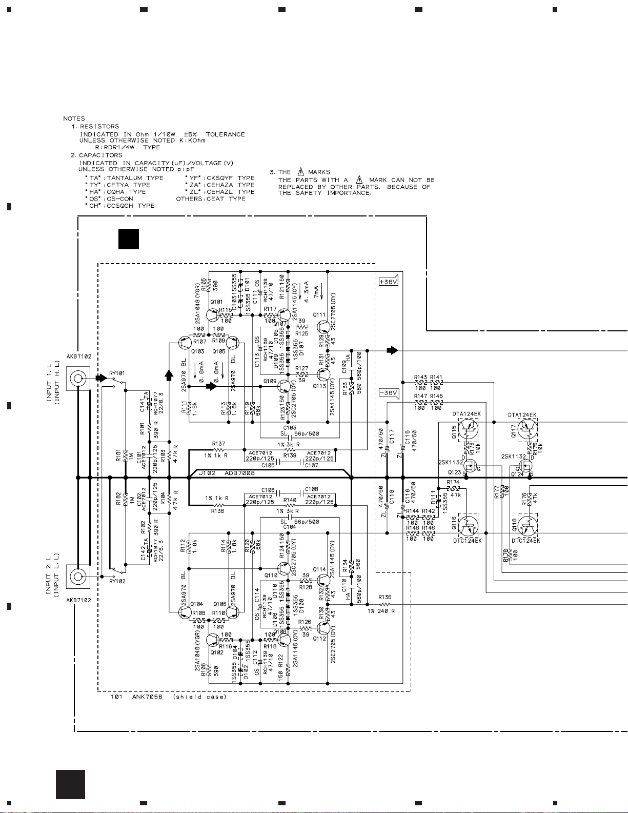
B
SEMICONDUCTORS
IC803 AEK7019
IC801,IC802 AEK7021
IC804,IC805 BA178M24T
Q815,Q816,Q819,Q820 2SA1255
Q803,Q804,Q811,Q812 2SA1837
Q805,Q806 2SA970
Q807,Q808 2SC2240
Q813,Q814,Q817,Q818 2SC3138
Q801,Q802,Q809,Q810 2SC4793
D801-D804 F10KF20
D805-D812,D833-D837 S5566G(TPB2)
D838 UDZS10B
Q821 2SC2712
D821-D828 1SS355
D829-D832 UDZ16B
D813-D816,D841-D844 UDZ24B
D817-D820 UDZ36B
COILS AND FILTERS
L801,L802 RTF1167
Mark No. Description Part No.
R819-R822 RS1/10S301J
R836-R838 RS1/10S3R3J
R805-R808 RS1LMF103J
Other Resistors RS1/10S J
OTHERS
CN805,CN806 10P MT CONNECTOR 1-173981-0
CN804 16P CONNECTOR 9604S-16C
H851,H852 FUSE CLIP AKR1004
CN851 AC CODE SOCKET RKP1751
CN852 AMP U-P CONNECTOR RKP1833
CN853 AMP U-P CONNECTOR RKP1834
SW ASSY
811-822 HEAT SINK ANH7100
805 PCB BINDER VEF1040
KN801-KN803 EARTH METAL FITTING VNF1084
C
SWITCHES AND RELAYS
S701 ASG-553
CAPACITORS
C701 (0.01µF/250V) ACE7014
OTHERS
CN701 AMP U-P CONNECTOR RKP1833
D
FRONT ASSY
SEMICONDUCTORS
IC902 BA178M05T
IC903 BA178M15T
IC904 AT24C01-10PC
IC901 PD5508B9
Q952 2SA1048
Q903,Q904 2SC2458
Q901,Q902 2SC2705
Q943,Q946 2SJ146
Q907-Q914,Q942,Q945 DTA124EK
Q918 DTA143EK
CAPACITORS
C851 (0.01µF/250V) ACE7014
C803,C804,C833 CEANP1R0M50
C829-C832,C836 CEAT100M50
C813-C820 CEAT100M63
C809-C812 CEAT471M2A
C821-C824 CEATR10M2A
C838,C840 CEHAT100M50
C839,C841 CEHAZA220M25
C825-C828 CEHAZL101M50
C834 CEHAZL182M35
C837 CEHAZL331M35
C805-C808 CEHAZL471M50
C842 CFTYA224J50
C801,C802 CKCYF103Z50
RESISTORS
R803,R804 RD1/4LMF470J
R813,R814 RD1/4MUF124J
R831,R839 RS1/10S100J
R815-R818 RS1/10S101J
Q915-Q917,Q919,Q926,Q928 DTC124EK
Q930,Q947-Q951 DTC124EK
Q932-Q935 DTC124ES
D933-D935,D953 1SS355
D927 DAN202K
D936 DAP202K
D901-D914 NSCW100-8511
D929-D932 SLP6118C51H
D951,D952 UDZS7.5B
COILS AND FILTERS
X901 (4.19MHz) VSS1014
SWITCHES AND RELAYS
S905 ASD7014
S901-S904 VSG1009
CAPACITORS
C921,C922,C942 CEHAZA220M25
C961,C963,C964 CEHAZA470M6R3
C941,C955,C957 CEJA100M35
C953 CEJA2R2M50
37
Page 38

M-AX10
Mark No. Description Part No.
C927,C954 CKSQYF103Z50
C901-C914,C923-C926 CKSQYF104Z50
C931-C934,C951,C956 CKSQYF104Z50
RESISTORS
Other Resistors RS1/10S J
OTHERS
902 3P CABLE HOLDER 51048-0300
901 7P CABLE HOLDER 51048-0700
CN901 16P CONNECTOR 52492-1620
J902 3P JUMP WIRE D20PDY0310E
J901 7P JUMP WIRE D20PDY0715G
E
LED ASSY
SEMICONDUCTORS
D752-D754 NSCW100-8511
RESISTORS
All Resistors RS1/10S J
OTHERS
CN751 3P JUMPER CONNECTOR 52151-0310
F
VR ASSY
SEMICONDUCTORS
IC761 TC74HC86AP
Q761,Q762 2SK1132
SWITCHES AND RELAYS
S761 ASX7028
CAPACITORS
C761 CEAT100M50
C762 CKSQYF104Z50
Mark No. Description Part No.
COILS AND FILTERS
L101 RTF1167
SWITCHES AND RELAYS
RY101-RY103 VSR1008
CAPACITORS
C101,C102,C105-C108 (220pF) ACE7012
C140 (47µF) ACH7116
C103,C104 CCCSL560K2H
C135 CCSQCH100D50
C132-C134 CCSQCH101J50
C128 CCSQCH470J50
C129,C130 CEAT100M50
C121,C122 CEHAZA101M25
C131 CEHAZA220M25
C125,C126 CEHAZL471M25
C115-C118 CEHAZL471M50
C119,C120,C123,C124 CFTYA104J50
C109,C110 CQHA561J2A
C141,C142 (22µF) RCH1077
C111-C114 (47µF/10V) RCH1139
C127 (100µF/6.3V) VCH1156
RESISTORS
R137,R138 RDR1/4VM1001F
R135,R136,R166 RDR1/4VM2400F
R139,R140 RDR1/4VM3001F
R101,R102 RDR1/4VM391J
R103,R104 RDR1/4VM473J
R157,R158 RS1/10S1002F
Other Resistors RS1/10S J
OTHERS
J101 6P HOUSING SHIELD WIRE ADX7253
JA101,JA102 PIN JACK(1P) AKB7102
CN101 11P SOCKET KP200TA11L
RESISTORS
All Resistors RS1/10S J
OTHERS
CN761 7P JUMPER CONNECTOR 52147-0710
G
INPUT (L) ASSY
SEMICONDUCTORS
IC101 DAC8043FP
IC102 OP275GP
Q101,Q102 2SA1048
Q120 2SA1145
Q119 2SC2705
38
Q107,Q108,Q113,Q114 2SA1145
Q103-Q106 2SA970
Q109-Q112 2SC2705
Q123,Q124,Q129-Q131 2SK1132
Q115,Q117,Q126-Q128 DTA124EK
Q116,Q118 DTC124EK
D101-D112 1SS355
D113,D114 UDZ18B
D115 UDZS5.1B
V. AMP (L) ASSY
H
SEMICONDUCTORS
Q325,Q326,Q341,Q342 2SA1162
Q309,Q310 2SA1929
Q301,Q302,Q307,Q308 2SA970
Q313,Q314,Q323,Q324 2SA970
Q303-Q306,Q315,Q316 2SC2240
Q321,Q322 2SC2240
Q327,Q328,Q343,Q344 2SC2712
Q329,Q331,Q332 2SC3326
Q311,Q312 2SC5170
Q333,Q334,Q339 2SK1132
Q335-Q337,Q340 DTA124EK
Q338 DTC124EK
D307,D313-D316 1SS355
D309-D312 UDZS7.5B
SWITCHES AND RELAYS
RY301,RY302 VSR1008
CAPACITORS
C303,C304,C333-C336 (220pF) ACE7012
C313,C314 (10µF) ACH7124
C301,C302,C319 (10µF) ACH7125
Page 39

M-AX10
Mark No. Description Part No.
C305-C308,C323-C326 CCSQCH270J50
C311,C312 CEAT470M25
C315-C318 CEGA471M50
C309,C310 CEHAZA470M10
C331 CFTYA683J50
C337,C338 CSZSR100M16
RESISTORS
R303,R304 RDM1/2P221J
R345 RDM1/2P3600F
R343,R344 RDM1/2P7500F
R341,R342 RDM1P3001F
R379,R380 RDR1/4PM470J
R301,R302 RDR1/4VM104J
R349-R352 RS1/10S101J
R315 RS1/10S1001D
R314 RS1/10S1101D
R386 RS1/10S30R0D
R385 RS1/10S33R0D
R313,R316,R325-R328 RS1/10S3900D
R347,R348 RS1/10S5100D
VR301,VR302 (220Ω) ACP7002
Other Resistors RS1/10S J
OTHERS
CN303 23P CONNECTOR 9604S-23C
J301 2WIRE SHIELD HOUSING ADX7258
J302 2WIRE SHIELD HOUSING ADX7259
KN301 EARTH METAL FITTING VNF1084
I
C. AMP (L) ASSY (AWX7673)
SEMICONDUCTORS
IC501,IC502 IC PROTECTOR(10A) AEK7022
Q503,Q504 2SA1162
Q517,Q518 2SC3138
Q507-Q510 2SC2712
Q513,Q515 2SK1132
Q511,Q512 DTA124EK
Q505,Q506 DTC143EK
Q501,Q502,Q519,Q520 IMX1
D501,D502 1SS355
D503,D504 BR3371XJ30A
COILS AND FILTERS
L501 RTF1167
SWITCHES AND RELAYS
RY501,RY502 ASR1035
CAPACITORS
C505,C506 CEANP470M10
C507 CEAT100M50
C508 CEHAZA220M25
C511,C512 CEHAZL471M50
C501-C504 CFTYA224J50
Mark No. Description Part No.
R503,R504 RS1/10S6801F
R509-R512,R531-R534 RS2LMFR22J
R521,R522,R537,R538 RS1/10S8201F
R513,R514 RS3LMF2R2J
VR501,VR502 (4.7KΩ) ACP7003
Other Resistors RS1/10S J
OTHERS
CN502 23P CONECTOR 9604S-23C
CN507,CN508 2P TOP POST B2B-EH
501 PCB BINDER VEF1040
KN501,KN502 EARTH METAL FITTING VNF1084
J
INPUT (R) ASSY
SEMICONDUCTORS
IC201 DAC8043FP
IC202 OP275GP
Q201,Q202 2SA1048
Q220 2SA1145
Q219 2SC2705
Q207,Q208,Q213,Q214 2SA1145
Q203-Q206 2SA970
Q209-Q212 2SC2705
Q223,Q224,Q229-Q231 2SK1132
Q215,Q217,Q226-Q228 DTA124EK
Q216,Q218 DTC124EK
D201-D212 1SS355
D213,D214 UDZ18B
D215 UDZS5.1B
COILS AND FILTERS
L201 RTF1167
SWITCHES AND RELAYS
RY201-RY203 VSR1008
CAPACITORS
C201,C202,C205-C208 (220pF) ACE7012
C240 (47µF) ACH7116
C203,C204 CCCSL560K2H
C235 CCSQCH100D50
C232-C234 CCSQCH101J50
C228 CCSQCH470J50
C229,C230 CEAT100M50
C221,C222 CEHAZA101M25
C231 CEHAZA220M25
C225,C226 CEHAZL471M25
C215-C218 CEHAZL471M50
C219,C220,C223,C224 CFTYA104J50
C209,C210 CQHA561J2A
C241,C242 (22µF) RCH1077
C211-C214 (47µF/10V) RCH1139
C227 (100µF/6.3V) VCH1156
C509 CFTYA474J50
C517,C518 CKSQYF104Z50
C515,C516 (47µF/10V) RCH1139
RESISTORS
R519,R520,R535,R536 RS1/10S1502F
R501,R502 RS1/10S1602F
RESISTORS
R237,R238 RDR1/4VM1001F
R235,R236,R266 RDR1/4VM2400F
R239,R240 RDR1/4VM3001F
R201,R202 RDR1/4VM391J
R203,R204 RDR1/4VM473J
39
Page 40

M-AX10
Mark No. Description Part No.
R257,R258 RS1/10S1002F
Other Resistors RS1/10S J
OTHERS
J201 6P HOUSING SHIELD WIRE ADX7253
JA201,JA202 PIN JACK(1P) AKB7102
CN201 11P SOCKET KP200TA11L
K
V. AMP (R) ASSY
SEMICONDUCTORS
Q425,Q426,Q441,Q442 2SA1162
Q409,Q410 2SA1929
Q401,Q402,Q407,Q408 2SA970
Q413,Q414,Q423,Q424 2SA970
Q403-Q406,Q415,Q416 2SC2240
Q421,Q422 2SC2240
Q427,Q428,Q443,Q444 2SC2712
Q429,Q431,Q432 2SC3326
Q411,Q412 2SC5170
Q433,Q434,Q439 2SK1132
Q435-Q437,Q440 DTA124EK
Q438 DTC124EK
D407,D413-D416 1SS355
D409-D412 UDZS7.5B
SWITCHES AND RELAYS
RY401,RY402 VSR1008
CAPACITORS
C403,C404,C433-C436 (220pF) ACE7012
C413,C414 (10µF) ACH7124
C401,C402,C419 (10µF) ACH7125
C405-C408,C423-C426 CCSQCH270J50
C411,C412 CEAT470M25
C415-C418 CEGA471M50
C409,C410 CEHAZA470M10
C431 CFTYA683J50
C437,C438 CSZSR100M16
RESISTORS
R403,R404 RDM1/2P221J
R445 RDM1/2P3600F
R443,R444 RDM1/2P7500F
R441,R442 RDM1P3001F
R479,R480 RDR1/4PM470J
R401,R402 RDR1/4VM104J
R449-R452 RS1/10S101J
R415 RS1/10S1001D
R414 RS1/10S1101D
R486 RS1/10S30R0D
Mark No. Description Part No.
L
C. AMP (R) ASSY (AWX7674)
SEMICONDUCTORS
IC601,IC602 IC PROTECTOR(10A) AEK7022
Q603,Q604 2SA1162
Q617,Q618 2SC3138
Q607-Q610 2SC2712
Q613,Q615 2SK1132
Q611,Q612 DTA124EK
Q605,Q606 DTC143EK
Q601,Q602,Q619,Q620 IMX1
D601,D602 1SS355
D603,D604 BR3371XJ30A
COILS AND FILTERS
L601 RTF1167
SWITCHES AND RELAYS
RY601,RY602 ASR1035
CAPACITORS
C605,C606 CEANP470M10
C607 CEAT100M50
C608 CEHAZA220M25
C611,C612 CEHAZL471M50
C601-C604 CFTYA224J50
C609 CFTYA474J50
C617,C618 CKSQYF104Z50
C615,C616 (47µF/10V) RCH1139
RESISTORS
R619,R620,R635,R636 RS1/10S1502F
R601,R602 RS1/10S1602F
R603,R604 RS1/10S6801F
R609-R612,R631-R634 RS2LMFR22J
R621,R622,R637,R638 RS1/10S8201F
R613,R614 RS3LMF2R2J
VR601,VR602 (4.7kΩ) ACP7003
Other Resistors RS1/10S J
OTHERS
CN602 23P CONNECTOR 9604S-23C
CN607,CN608 2P TOP POST B2B-EH
601 PCB BINDER VEF1040
KN601,KN602 EARTH METAL FITTING VNF1084
R485 RS1/10S33R0D
R413,R416,R425-R428 RS1/10S3900D
R447,R448 RS1/10S5100D
VR401,VR402 (220Ω) ACP7002
Other Resistors RS1/10S J
OTHERS
CN403 23P CONNECTOR 9604S-23C
J401 2WIRE SHIELD HOUSING ADX7258
J402 2WIRE SHIELD HOUSING ADX7259
KN401 EARTH METAL FITTING VNF1084
40
Page 41

6. ADJUSTMENT
Table 6-3 DC offset adjustment method
Channel
Adjustment
Point
Measurement Point
Adjustment
Value
L High ch VR301
Apply channel speaker
terminals (Red, Black)
0V ± 10mV
L Low ch VR302
R High ch VR401
R Low ch VR402
M-AX10
6.1 IDLE CURRENT ADJUSTMENT
The idle current is adjusted in two steps: coarse and fine. Note that
the adjustment value for fine adjustment depends on the elapsed
time from the coarse adjustment.
For the points to be adjusted or measured, see Table 6-1 and Fig. 6-
1.
For the adjustment timing and values, see Table 6-2.
Be sure to turn VR501, VR502, VR601 and VR602 fully counterclockwise before turning the power on.
Table 6-1 Adjustment points of idle current
Channel L High ch L Low ch R High ch R Low ch
Adjustment
point
Measurement
point
Table 6-2 Adjustment values of idle current
Coarse
Adjustment
Fine
Adjustment
VR501 VR502 VR601 VR602
CN505 CN505 CN605 CN605
Between
pins 1 and 2
Adjustment Timing
Power ON immediately 14.5mV ± 1.0mV
Elapsed
time from
the coarse
adjustment
Between
pins 3 and 4
More than 5 min.
and less than
10 min.
More than 10 min.
and less than
15 min.
More than 15 min.
and less than
30 min.
More than 30 min.
pins 1 and 2
Between
Adjustment value
(Pin voltage)
16.0mV ± 0.5mV
15.5mV ± 0.5mV
15.0mV ± 0.5mV
14.5mV ± 0.5mV
Between
pins 3 and 4
6.2 DC OFFSET ADJUSTMENT
Adjust the DC offset with the power on immediately before fine
adjustment of the idle current.
For the points to be adjusted or measured, and the adjustment values,
see Table 6-3 and Fig. 6-1.
6.3 OPERATION CHECK OF THE
PROTECTION CIRCUIT
While supplying a sine wave of 1 Hz, 1.2 Vrms in DUAL MODE,
with ATT.THROUGH OFF, increase the volume level and check
that the protection circuit activates before the level reaches the
maximum value. It works about before twelve o'clock position.
CAUTION : This check mode may damage the speaker(s) when it
is connected to the output terminal. It is recommended
that output terminal is open at this check mode.
VR302
L Low ch
DC OFFSET ADJ
VR301
L High ch
DC OFFSET ADJ
VR502
L Low ch
Idle Current ADJ
VR501
L High ch
Idle Current ADJ
CN505
Rear Side
Front Side
Fig. 6-1 Adjustment and measurement points
CN605
VR402
R Low ch
DC OFFSET ADJ
VR401
R High ch
DC OFFSET ADJ
VR602
R Low ch
Idle Current ADJ
VR601
R High ch
Idle Current ADJ
41
Page 42

M-AX10
7. GENERAL INFORMATION
7.1 IC
• The information shown in the list is basic information and may not correspond exactly to that shown in the schematic diagrams.
List of IC
•
PD5508B9, DAC8043FP
PD5508B9 (FRONT ASSY : IC901)
• Control Microcomputer
Pin Function
•
No. Mark Pin Name I/O Pin Function
1 P53 VR2 I
2 P17/Srdy/A10 LD O
3 P16/CLK/A9 CLK O
4 P15/Sout/A8 SRD O
5 P14/Sin/A7 IND. IN1 O
6 P13/T1/A6 IND. IN2 O
7 P12/T0/A5 IND. SEPA O
8 P11/A4 IND.BRD O
9 P10 IND. DUAL O
10 P27/IN7 IND. ATT.THROUGH O
P26/IN6
11
12 P25/IN5 INPUT2 O
13 P24/IN4 DACVR O
14 P23/IN3/A3 SEPARATE O
15 P22/IN2/A2 INVERT O
16 P21/IN1/A1 SPRYH O
17 P20/IN0/A0 SPRYG O
18 Vref/CE Vref 19 Xin Xin I
20 Xout Xout O
21 Vss Vss 22 Vcc Vcc 23 P50/Xcin VR4 I
24 P51/Xcout VR5 I
25 RESET RESET I
26 P30/INT0/A11 BACKUP I
27 P31/INT1/A12 BRD. I
28 P32/CNTR0/OE DAL. I
29 P33/CNTR1/Vpp VR1 I
30 P40/A13 SEPA I
31 P41/A14 FMT O
32 P42 ILL2 O
33 P43 ILL1 O
34 P00/D0 SDA I/O
35 P01/D1 SCL O
36 P02/D2 MD WKUP I
37 P03/D3 ATT. THROUGH I
38 P04/D4 ATT. HOLD I
39 P05/D5 INPUT I
40 P06/D6 ILL. I
41 P07/D7 P-DET I
42 P52 VR3 I
IND. ATT. HOLD
Serial I/O pins
Timer output
O
Analog input
Reference voltage input
Clock input
Clock output
Power supply voltage input
Power supply voltage input
Reset input
External inrerrupt input
Timer input
Key ON wake-up function
42
Page 43

M-AX10
Following item "1."~"7." (P.43~P.51) describe about the specifications
of IC901 PD5508B9.
SPECIFICATIONS
1. Basics
1.1 Reset
Perform the reset when connecting the AC power supply.
RESET
RAM set complete flag of EEPROM readout data
[ f_eeprom_rd_set ] = 0
AC check (Voltage of ACSUB)
Register initialize
RAM initialize
EEPROM readout
BACKUP
check OK ?
N
RAM clear for memory communication
Y
1.2 BACKUP Mode
Backup is performed when the AC power is turned off.
SPRYH (port 16) and SPRYG (port 17) are set to "L" 10 ms after
the BACKUP port becomes "L."
All the indicators and lamps go dark.
Execution of the BACKUP processes (port processing and register
processing) begins 30 ms later.
Last memory writing to the EEPROM is performed each time a key
is operated, but not performed in the backup processes.
Port processing
1) I/O ports are specified as output ports.
2) Output ports are set to "L."
Backup targets
INPUT1/2, ATT.THROUGH, ATT. HOLD (The level value is also
backed up when ON), ILL.
(The VOLUME level and mode settings at the mechanical switch
are checked each time the power is turned on.)
BRD. DUAL
ILL
INPUT
ATT. THR
ATT. HOLD
ATT. LEVEL
Bright / dark / off
1/2
ON/OFF
As writing to ROM may require 40 ms at maximum, 5 V will be
supplied to the microcomputer for about 100 ms after the AC power
is turned off at the hardware.
The data to be written are composed of the following 3 bytes:
PRO.
ON/OFF
At ATT. HOLD
ON only
Flag for the power ON [ f_power ] = 1
Flag for initializing [ f_i nit ] = 1
Timer [ tminit ] = 50 msec set
RETURN
Fig. Flow chart of RESET
(IC901
Internal Port)
Perform reading from the EEPROM while RAM is being initialized
after the AC power is turned on (port 25 (Pin25) (RESET): L).
Set the read data to RAM using "initcont" after resetting is completed.
(See "2. Initializing.(P.44)")
1 Bit 0
Bit 1
Bit 2
Bit 3
Bit 4
Bit 5
Bit 6
Bit 7
2
3
ILL1 ON/OFF
ILL2 ON/OFF
INPUT 1/2
ATT. THROUGH ON/OFF
ATT. HOLD ON/OFF
SEPARATE ON/OFF
DUAL ON/OFF
BRIDGE ON/OFF
VOLUME position (5 bit)
* At ATT. HOLD ON only
BACKUP code
Communication is made using ports 34 (SDA) and 35 (SCL) as
output ports.
IC901 PD5508B9
43
Page 44

M-AX10
1.3 Last Memory
Last memory writing to the EEPROM (IC904:AT24C01-10OC) is
performed each time a key is operated.
Input-independent last memory is not provided.
The ILL and ATT.THROUGH settings remain the same in switching
between INPUT 1 and 2.
1.4 TEST Mode
None
1.5 SILENT Mode
The unit can enter SILENT mode in a condition other than the
following:
• The BACKUP port is "L." (BACKUP mode)
• A volume operation is being processed.
• A key input is being processed.
• Caution status for mode switching (caution indication state at the
operation of OPERATION MODE SW during Power-On state)
When 200 ms have elapsed after such a process is completed, the
unit can enter SILENT mode.
The unit restarts upon key input, a volume operation, mode switching,
or P-DET input.
The timer is set for 5-second restarting.
When 200 ms have elapsed after the restarting process is completed,
the unit can enter SILENT mode again.
(SILENT mode : The control µ-com enter the low power consump tion mode and stops the oscillation of system clock.)
(normal operation mode)
(2) POWER OFF
Port 16 (SPRYH)(Pin16) is set to "L" 10 ms after POWER OFF
(port 26 (BACKUP)(Pin26) becomes "L").
Ports that must be processed other than port 16 are operated
immediately after this.
26 (BACKUP)
16 (SPRYH)
10 msec
2. Initializing
The main routine starts after reset processing.
Normal processing starts after the initializing process is completed
with "initcont".
The data read during the reset processing are written to RAM.
(See the "1. Basics"(P.43).)
If the MODE switch was not operated during the POWER OFF
period, the read data are written to RAM.
If the MODE switch was operated during the POWER OFF period,
the default settings are made.
Default: INPUT1
ATT.THROUGH OFF
ATT.HOLD OFF
ILL Bright
1.6 POWER ON/OFF
(1) POWER ON
After POWER ON, port 16 (SPRYH)(Pin16) is set to "L" and port
31 (FMT)(Pin31) is set to "H."
Port 31 (FMT) is set to "L" after 3 seconds, and muting is set to
OFF.
After another 5 seconds (8 seconds after POWER ON), ports 16
(SPRYH) and 17 (SPRYG)(Pin17) are set to "H," and relay is set to
ON.
Power ON
16 (SPRYH)
31 (FMT)
3 sec 5 sec
Then the timers are set.
Refer to the next page Fig.1.
IC901 PD5508B9
44
Page 45

Reset
M-AX10
AC check
Register initial setting
RAM initial setting
when EEPROM read
out is OK.
RAM initial setting
when EEPROM read
out is NG.
Timer [tminit]
INITCONT processing
Relay
Timer [tmprot]
MUTE
Timer [tmmute]
200 msec
1
2
3
4
50 msec
5
INITCONT start
6
ACTION start
#
3 sec
$
8 sec
INPUT SW set
LED lights processing
ATT. through SW set
MODE SW set
ILL. lights processing
DAC VOL transfer
processing
At ATT. through ON
At ATT. through OFF
Tact key accept start
Timer [tmdcerr]
Silent mode
7
8
100 msec
9
0
-
40 msec
~
2 sec
=
!
5 sec
@
Fig.1 Timing chart of initializing process from the reset
200 msec
%
45
Page 46

M-AX10
3. Key Input (IC901)
36 (MD WKUP)
IC901
Microcomputer
37 (ATT.THROUGH)
38 (ATT.HOLD)
39 (INPUT)
40 (ILL)
IC901 PD5508B9
SW1 SW2
Key input, indicators and processes
Key Input
Port
37
(ATT. THROUGH)
39
(INPUT)
38
(ATT. HOLD)
40
(ILL)
ACT
L
L
L
Indicator
Process Port
10
(IND ATT. THROUGH)
5 (IND IN1)
6 (IND IN2)
11 (IND ATT. HOLD)
None
SW3 SW4 SW5
Contents of Process
DUAL BRIDGE
Alternates "H" and "L"
alternately at each key
input.
Sets INDIN1 and INDIN2 to
"H" and "L" alternately at
each key input.
Key disabled. Always "L". Key disabled. Always "L". Alternates "H" and "L" at
Alternates "H" and "L"
alternately at each key
input.
Sets INDIN1 and INDIN2
to "H" and "L" alternately
at each key input.
SEPARATE
Alternates "H" and "L"
alternately at each key
input.
Key disabled with
ATT.HOLD ON.
Key disabled.
Both INDIN1 and INDIN2
always lit ("H").
each key input.
Key disabled with ATT.
THROUGH ON.
Key Input
Port
37
(ATT. THROUGH)
39
(INPUT)
38
(ATT. HOLD)
40
(ILL)
46
ACT
L
L
L
L
Indicator
Process Port
13 (DAC VR)
12 (INPUT2)
32 (ILL2)
33 (ILL1)
Contents of Process
DUAL BRIDGE
ON : "H"
OFF : "L"
INPUT1 : "L"
INPUT2 : "H"
Key disabled. Key disabled.
Cycles Bright/Dark/Off at each key input.
(ILL1, ILL2) Bright (H, L)
Dark (L, H)
Lamp Off (H, H)
LED Off (L, L)
Factory setting: Bright (H, L)
ON : "H"
OFF : "L"
INPUT1 : "L"
INPUT2 : "H"
SEPARATE
ON : "H" (VOL invalid)
OFF : "L" (VOL valid)
Key disabled with ATT.
HOLD ON.
Fixed at L.
ON : HOLD data valid
VOL invalid
OFF : VOL valid
Key disabled with ATT.
THROUGH ON.
Page 47

M-AX10
3.1 Key Inputs
A key input becomes valid after 40 ms, to eliminate chatter.
The ATT.THROUGH key input from OFF to ON becomes valid
when the key is held pressed for 2 seconds.
3.2 Switch inputs
The MODE switch (rotary switch) setting is read when the power is
turned on.
The switch operation with POWER ON is invalid.
(See "7. WARNING."(P.50))
4. KEY PROCESSING (IC901)
4.1 ATT.THROUGH Switching
The ATT.THROUGH key input from ON to OFF becomes valid
when the key is held pressed for 2 seconds.
Any other key input during these 2 seconds is invalid.
When switching from OFF to ON, the key input becomes valid at
normal timing.
Key input valid
Port 16 (SPRYH)(Pin16) is set to "L" 10 ms after ATT.THROUGH
switching signal input, and relay is set to OFF.
After another 30 ms, the INDICATOR port is processed.
Port 31 (FMT)(Pin31) is set to "H," and muting is set to ON.
Switching process is performed 100 ms after ATT.THROUGH
switching signal input.
When switching ATT THROUGH from ON to OFF:
Data transfer to the DAC IC is performed 2 seconds after the key
input.
When switching ATT.THROUGH from OFF to ON:
Port 2 (LD), port 3 (CLK), and port 4 (SRD) are fixed to "L" before
DACVR (pin 13) is set to "L," 30 ms after relay becomes OFF.
(See "6. DAC Volume Transfer."(P.49))
After another 2 seconds, port 31 (FMT)(Pin31) is set to "L," and
muting is set to OFF.
After another 3 seconds, port 16 (SPRYH)(Pin16) is set to "H," and
relay becomes OFF.
EEPROM writing
Relay
Mute
LED ON/OFF
processing
Switching
VOL. processing
(ON → OFF)
VOL. data line processing
(OFF → ON)
Silent processing
1
2
10 msec
4
6
7
100 msec
9
40 msec
5
40 msec
2 sec
8
2 sec
3
5 sec
Fig.2 Timing chart when ATT. through key is pressed
200 msec
0
47
Page 48
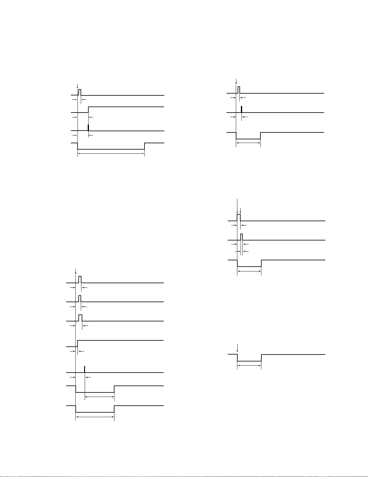
M-AX10
4.2 INPUT switching
INDICATOR port processing and switching process start 30 ms
after INPUT key input [port 39 (INPUT)(Pin39): "L"].
No muting process is performed.
INPUT key is pressed.
EEPROM writing
1
LED processing
40 msec
2
Switching processing
40 msec
3
Silent processing
4
Fig.3 Timing chart when INPUT key is pressed
4.3 ATT.HOLD Key Processing
Upon ATT.HOLD key input, the specified current volume value
is held.
While ATT.HOLD is ON, the volume level stays at the held value
even if the volume control is operated.
In Muting mode (when the power is turned on or ATT.
THROUGH is switched from ON to OFF), the ATT.HOLD key is
disabled.
4.4 ILL Key Processing
Each press of the key cycles Bright, Dark, Lamp Off, and LED
Off.
ILL key is pressed
1
Port processing
2
SILENT processing
3
Fig.5 Timing chart when ILL key is pressed
4.5 VOL Key Processing
VOL operation
VOL input valid
typ. 15 msec
1
Data transfer
to DAC
typ. 16 msec
2
3
ATT. HOLD key is pressed.
EEPROM writing
(OFF → ON)
EEPROM writing
(ON → OFF)
VOL. transfer
(ON → OFF)
LED processing
HOLD processing
(OFF → ON)
SILENT
(OFF → ON)
typ. 8 msec
1
typ. 1 msec
2
typ. 10 msec
3
typ. 0 msec
4
5
6
SILENT
(ON → OFF)
6’
Fig.4 Timing chart when ATT. HOLD key is pressed
SILENT processing
Fig.6 Timing chart when volume is input
4.6 Invalid Key Input
An invalid key is pressed.
SILENT processing
Fig.7 Timing chart when an invalid key is pressed
4
1
5 sec
5 sec
48
Page 49

5. Mode Switching Processing (IC901)
Select the mode of the speakers using the MODE switch (rotary
switch).
Any of three modes (BRIDGE, DUAL and SEPARATE) can be
selected.
Table Mode select indicator processing
Mode
Input Port
27
(BRIDGE)
28
(DUAL)
30
(SEPA.)
Table Mode select port processing
Mode
Input Port
27
(BRIDGE)
28
(DUAL)
30
(SEPA.)
ACT
L
L
L
Indicator
Process Port
8 (IND BRD.)
9 (IND DUAL)
7 (IND SEPA.)
Contents of Process
Sets to "H".
Sets to "H".
Sets to "H".
ACT
12 (INPUT2)
INPUT1 : "L" ATT. through : "L"
L
INPUT2 : "H"
INPUT1 : "L" ATT. through : "L"
L
INPUT2 : "H"
Fixed at "L"
L
13 (DACVR) 14 (SEPARATE) 15 (INVERT) 16 (SPRYH) 17 (SPRYG)
ATT. exist : "H" ATT. exist : "H"
ATT. exist : "H" ATT. exist : "L"
ATT. through : "L"
ATT. exist : "H" ATT. exist : "L"
Contents of Process
Process Port
IC901 PD5508B9
"L" "H" "L"
"L" "H" "L"
"H" "H" "L"
ATT. through : "H"
ATT. through : "L"
ATT. through : "L"
M-AX10
The MODE switch is disabled while power is ON.
(See "7. WARNING.")
6. DAC Volume Transfer (IC901)
When the status of port 29 (VR1) changes, port 29 (VR1), port 30
(VR2), port 42 (VR3), port 23 (VR4), and port 24 (VR5) are
checked to detect the VOLUME position.
With DUAL, BRIDGE, or SEPARATE, the attenuation volume is
read from the VOLUME position/ATT volume table and
transferred to the DAC IC in Serial mode (MSB first).
When the transfer is completed, LD (port 2) is set to "L" then
returned to "H."
When ATT.THROUGH is ON or port 13 (ATT.THROUGH) is
"L," port 2 (LD), port 3 (CLK), and port 4 (SRD) are fixed at "L."
Then the data are transferred again when port 13 (
is set to "H."
When switching ATT.THROUGH from ON to OFF or when
turning power ON:
Data transfer is performed 2 seconds after the switch is operated.
Switching
DACVR (pin 13)
ATT.THROUGH
When switching ATT THROUGH from OFF to ON or when
turning the power ON:
Port 2 (LD), port 3 (CLK), and port 4 (SRD) are fixed at "L"
before DACVR (pin 13) is set to "L," 30 ms after relay becomes
OFF.
Relay
Three data lines
"L"
)
DACVR (pin 13)
Data transfer is performed once in the following conditions and
terminated:
• When the power is turned on
• When the VOL is operated
• When ATT.THROUGH is switched from ON to OFF
• When ATT.HOLD is switched from ON to OFF
Data transfer
2 sec
49
Page 50

M-AX10
Position
31
30
29
28
27
26
25
24
23
22
21
20
19
18
17
16
15
14
13
12
11
10
9
8
7
6
5
4
3
2
1
Binary
Code
00000
00001
00010
00011
00100
00101
00110
00111
01000
01001
01010
01011
01100
01101
01110
01111
10000
10001
10010
10011
10100
10101
10110
10111
11000
11001
11010
11011
11100
11101
11110
BRIDGE / DUAL
Attenuation (dB) Serial Data
0
-2
-4
-6
-8
-10
-12
-14
-16
-18
-20
-22
-24
-26
-28
-30
-32
-34
-36
-38
-40
-42
-44
-46
-48
-50
-52
-54
-56
-58
Infinity
FFF
CB4
A17
804
65E
50E
404
331
289
203
199
145
102
CD
A3
81
66
51
40
33
28
20
19
14
10
C
A
8
6
5
0
-2.0021
-4.0026
-6.0015
-8.0013
-10.0064
-12.0052
-14.0006
-16.0002
-18.0089
-20.0106
-22.0074
-24.0127
-26.0100
-28.0013
-30.0333
-32.0731
-34.0754
-36.1215
-38.0937
-40.2039
-42.1421
-44.2863
-46.2245
-48.1627
-50.6615
-52.2451
-54.1833
-56.6821
-58.2657
#NUM!
PROCESSOR
Attenuation (dB) Serial Data
0.0
-0.5
-1.0
-1.5
-2.0
-2.5
-3.0
-3.5
-4.0
-4.5
-5.0
-5.5
-6.0
-6.5
-7.0
-7.5
-8.0
-8.5
-9.0
-9.5
-10.0
-10.5
-11.0
-11.5
-12.0
-12.5
-13.0
-13.5
-14.0
-14.5
-15.0
FFF
F19
E41
D75
CB4
BFE
B53
AB0
A17
987
8FE
87D
804
791
725
6BE
65E
603
5AC
55B
50E
4C6
482
441
404
3CB
394
361
331
303
2D8
-0.5021
-1.0016
-1.5013
-2.0021
-2.5023
-3.0001
-3.5028
-4.0026
-4.5008
-5.0030
-5.5039
-6.0015
-6.5025
-7.0008
-7.5043
-8.0013
-8.5003
-9.0057
-9.5043
-10.0064
-10.5037
-11.0010
-11.5045
-12.0052
-12.5007
-13.0072
-13.5048
-14.0006
-14.5040
-15.0025
7. WARNING
7.1 Protection
When abnormal amplifier output is detected, the protection relay
and function muting are controlled to warn the user.
When P-DET (port 41) becomes "L," FMT (port 31) is set to "H"
and port 16 (SPRYH) is set to "L" immediately.
At the same time, ILL indicators flash in 1-second cycle.
(ILL1, ILL2) = (H, L) ↔ (L, L) (ILL1=port33(Pin33)
Flashing : Mode illumination light ILL2=port32(Pin32))
Mode indicator
Panel light
When the POWER OFF key is pressed, POWER OFF processing is
performed. (All other keys are disabled.)
Refer to 7.2 PROTECTION CIRCUIT about the circuit explanation.
7.2 Mode Switching
Mode switching is allowed only when the power is OFF.
If mode switching is performed with the power ON, relay is set to
OFF. When the previous status is restored, relay is returned to ON.
As a caution, the LED of the selected mode and the LED of the
operating mode flash with the timing shown below.
When the MODE switch is returned to its original setting, the LED
flashing as a caution stops, and normal status is resumed.
The MODE switch is read every loop.
When the MODE switch is operated when the ILL indicator is dark,
the indicator is forcibly turned on.
When the MODE switch setting matches the operating mode setting,
the ILL mode resumes its original status.
Relay is set to OFF in the MODE CAUTION status.
Indicator of the
operating mode
Indicator after
the switch is
operated
0.5
sec
1.0 sec
ON
OFF
ON
OFF
50
Page 51

M-AX10
Switching
Acknowledgment
of switching
[f_mderr_rq]
Flag for Mode error
LED Warning
ILL lights if it is off
Mode error LED
warning
Key disabled
Relay
ILL processing
Silent mode
Fig.8 Timing of mode switching error processing
Switching
(restoring the original setting)
20 msec 20 msec
10 msec
200 msec
7.3 Warning when switching ATT.THROUGH from
OFF to ON
When ATT.THROUGH is switched from OFF to ON, the key
becomes valid when it is held pressed for 2 seconds.
The ATT.THROUGH ON/OFF LED flashes during those 2 seconds.
IC901 PD5508B9
DAC8043FP (INPUT(L) ASSY : IC101, INPUT(R) ASSY : IC201)
• D/A Converter IC
Pin Assignment (Top View)
•
V
REF
1
R
FB
2
3
I
OUT
4
GND
Block Diagram
•
V
REF
CLK
SRI
LD
5
V
DD
6
CLK
7
SRI
8
LD
2
R
1
12-BIT
D/A CONVERTER
FB
3
12
5
12-BIT
DAC REGISTER
8
12
7
6
12-BIT INPUT
SHIFT REGISTER
4
R
FB
I
OUT
V
DD
GND
51
Page 52

M-AX10
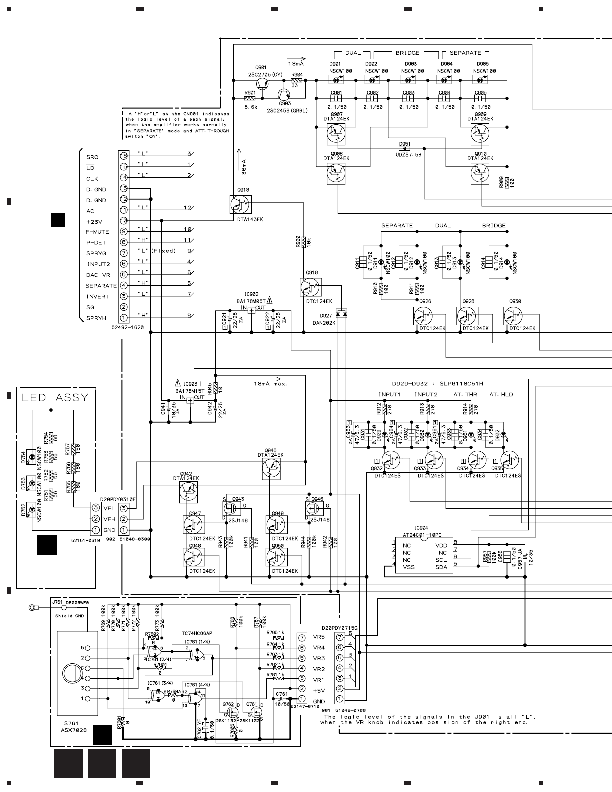
7.2 PROTECTION CIRCUIT
The protection circuits are provided for this unit. When these protection
circuits are activated ,the hardware muting is activated and muting and the
output relays are controlled by the microcomputer.
There are two protection circuits.
1) DC voltage detection at the output
2) Overcurrent detection due to the short circuit at the load end
1. DC voltage detection circuit
At the High-CH (Low-CH) output current amp of C.AMP (L)ASSY,
DC voltage is detected by Q507 and Q509 (Q508 and Q510) and these
transistors turned ON and P-DET signal becomes Low. When P-DET
signal becomes Low ,relay control Tr. Q515 ,Q511 and Q512 becomes
open and shut down the relay RY501 and RY502. Also microcomputer
receive P-DET Low signal and activate the mute circuit and set OFF the
relay control Tr. Q513.
2. Overcurrent detection circuit
At the High-CH (Low-CH) output current amp of C.AMP (L)ASSY,
(+) side overcurrent is detected by Q503 and Q505 (Q518,Q504 and
Q506) and these transistors turned ON and P-DET signal becomes Low.
Following is same as above.
(–) side overcurrent is detected by Q517,Q503 and Q505 (Q504 and
Q506) and these transistors turned ON and P-DET signal becomes Low.
Following is same as above.
Refer to next page FIg.1 about the circuit description.
3. Starting condition of the protection circuit
The above protection circuits works under the following condition.
DC voltage detection : about over ± 3V
Overrcurrent detection : about over 14~15A
52
Page 53

M-AX10
+23V
DC VOLTAGE DETECTION CIRCUIT
P-DET
OVERCURRENT DETECTION CIRCUIT
+HOUT L
[H – CH L]
–HOUT L
+LOUT L
[L – CH L]
–LOUT L
DC VOLTAGE DETECTION CIRCUIT
Fig.1 PROTECTION CIRCUITS
OVERCURRENT DETECTION CIRCUIT
P-DET
SPRYH
To
U-com IC901
(KU/CA : AWX7673)
( NY : AWX7280)
C.AMP (L) ASSY
53
Page 54

M-AX10
7.3 DESCRIPTIONS
7.3.1 Product Overview
Features of this product
Three-mode drive power amplifiers
This product is equipped with power amplifiers for two right and
two left channels (total of 4 channels).
Three types of speaker drive formats can be selected.
1. SEPARATE mode
The product functions as a 4-channel power amplifier (115 watts, 4
ohms for each of 4 channels). By connecting to a 2-way channel
divider, a high-grade multi-amplifier system can be established.
Using two units of this product provides a Hi-Fi surround system
for up to 8 channels. The product can also be used for DVD multichannel audio, DOLBY DIGITAL, and DTS applications.
2. DUAL mode
By connecting speakers that conform to tandem-wiring use, a Biamplifier (tandem amplifier) system can be established. By driving
tweeters and woofers separately with different amplifiers,
interference between speaker units is virtually eliminated. Thus,
super hi-fi stereo playback with a high degree of purity is enabled.
3. BRIDGE mode
The product functions as bridge-output high-power amplifiers (230
watts, 6 ohms for each of 2 channels).
Symmetrical twin-stereo structure
High-performance stereo amplifiers are symmetrically mounted left
and right.
Of course in SEPARATE or DUAL mode, enlargement of a large
current loop can be eliminated even in BRIDGE mode, restraining
sound degradation due to magnetic coupling, which is a disadvantage
of bridge amplifiers. The important parts are isolated by shield plates
and shield cases to achieve excellent channel separation at high
frequencies (104 dB or more at 20 kHz between the left and right
channels). You can enjoy high-grade stereophonic playback in a
rich sound field.
Advanced direct-energy MOSFET power
amplifiers
This product employs MOSFETs of larger capacity than with
conventional models. For insulation between each large heat sink
and MOSFET, a quite small zero-resistance ceramic sheet is
employed to improve the radiation characteristics. Not only a rise
in temperature with continuous signal input, but also instantaneous
rises in temperature with pulse-type input can be minimized.
For higher sound quality, the response speed to an input of large
sound volume and the clarity are highly improved.
In addition, a newly developed Z (ZETT) BIAS circuit that precisely
reproduces the thermal factors of a MOSFET is mounted for
temperature compensation for the idle current. This drastically
improves the drift of the idle current which may greatly affect sound
quality, and enables playback at constantly stable sound quality
immediately after you turn on the power.
Wide-range linear circuit
The wide range linear circuit has been enhanced to improve DC
stability by newly employing highly accurate parts of 0.5% error
and single-chip dual transistors for a completely discrete structure
that uses no DC servo or operational amplifier.
This enables natural and clear playback of low frequencies by
keeping NFB stable from very low frequencies.
DAC (Digital Accurate Control) attenuator
A high-precision 12-bit D/A converter of ladder resistance type is
used.
Advantages of the DAC attenuator (when compared with
conventional mechanical sliding-type controls)
1. Excellent S/N in practical usage
2. The frequency response is not affected by the attenuation volume
setting.
3. The attenuation volume can be programmed. This product
provides two curves, for high-frequency attenuation in a multiamplifier system and for normal volume control.
4. No tracking error (gain error between channels)
5. No signal irregularity from vibration, providing pure sound
6. The operation block and the circuit block can be separated. The
signal path length can be minimized by free layout.
Large-sized super ring toroidal transformer
A large-sized super ring toroidal transformer of 450 VA is employed
for the lowest possible loss and lowest impedance at the power block.
In addition, repression of power harmonics, which has been regarded
as impossible with large-capacity toroidal transformer, has been
achieved, enabling powerful and smooth playback at high speeds.
Silent control microcomputer
When the knobs and buttons are not operated, the control
microcomputer enters Low-Power-Consumption mode (system clock
oscillation stops). This decreases power consumption, and eliminates
high-frequency interference caused by clock oscillation to maintain
high sound quality. In addition, the microcomputer continuously
monitors the amplifier status and if it detects an abnormality, it
immediately activates the protection circuit. By using the
microcomputer in combination with the conventional hardwareprotection circuit, higher reliability and safety are ensured.
Ultra-Low-Impedance Power Circuit
Power de-coupling by an ultra-low-impedance condenser, ample
jumper lines and a No. 16 wire power cable are employed for very
low impedance in the power and ground lines.
In the low frequency range, channel separation is greatly improved
(achieving 115 dB at 20 Hz) by decreasing ground common
impedance.
In the high frequency range, the rise in impedance due to the
inductance component is suppressed, for higher frequency stability.
Thus a power amplifier that is virtually impervious to changes in
speaker impedance and connection cables has been created.
54
Page 55

7.3.2 Circuit Description
Block Diagram
BRIDGE
37.1V(200W)/6Ω20V(100W)/4Ω
OUTPUT VOLTAGE
DUAL
SEPARATE
Red
Low ch
Blk
Bridge
Blk
High ch
Red
10A(/KU/CA)
4A (/NY)
±30V Power Amp Current Stage
(Full-wave voltage doubler rectifier)
M-AX10
AC IN
~–
+~
14dB POWER AMP
12dB FLAT AMP
+
–
MUTE
+
–
24V
LED
24V
RY
15V
LED
LED
AC
5V
Microcomputer
Protection circuit
detection
±40V Power Amp Current
MUTE
+
–
Vref
Iout
Microcomputer
Stage FLAT AMP
±18V Op Amp IC
+5V
for Lch
(for Rch same as L ch)
DAC IC
LOCAL
CIRCUT
ON/OFF
+
–
+
–
INDICATOR
ATT
CONTROL
FUNC MUTE
MODE RY
INPUT RY
PROTECTION RY
Input 2
(Low ch)
Microcomputer
Silent
microcomputer
1V/50kΩ
Input 1
(High ch)
Interruption
ATT DATA input
µ-COM
KEY input
MODE SW
Protection circuit
Backup
detection
AC ON/OFF information
BACK UP RESET
EEPROM
55
Page 56

M-AX10
Each mode of block diagram
IN 2
IN 1
IN 2
IN 1
12dB
+
12dB
+
12dB
+
12dB
+
DAC VR
– Dual Drive Mode –
14dB
+
14dB
+
14dB
+
14dB
–
RED
BLK
RED
BLK
RED
BLK
RED
BLK
Low ch
High ch
Full
Range
Low ch
High ch
12dB
+
12dB
+
DAC VR
– Bridge Drive Mode –
14dB
14dB
DAC VR
– Separate Drive Mode –
+
+
RED
Low ch
BLK
RED
High ch
BLK
56
Page 57

Descriptions of the Block Diagram
1. INPUT switching block
Four small-signal relays for individual channels are used for input
signal switching.
2. 12-dB flat amplifier block
The input signal is amplified by 12 dB (4 times) to increase the
input level at the DAC attenuator block to improve the dynamic
range and signal-to-noise ratio.
In DUAL or BRIDGE mode, the flat amplifier on the low-channel
side is shut down by the LOCAL CIRCUIT OFF circuit.
The circuits are mounted in a shielded box to completely eliminate
electrostatic and magnetic coupling.
3. DAC attenuator block
Attenuator section
This is a digitally controlled high-precision analog attenuator that
uses a ladder resistance block of R-2R-type DAC ICs for volume
control. The signal is input to the Vref (reference-voltage) terminal
and the attenuated signal current is obtained from the Iout (currentoutput) terminal. The signal at this terminal is converted to a voltage
signal by an I-V converter of the operational amplifier. An output
signal of the same phase as the input signal is obtained through
inversion by the operational amplifier. The attenuation volume
adjustment is controlled using serial data from the microcomputer.
M-AX10
5. Protection circuit
When a DC voltage at the output end or a short circuit at the load
end is detected, hardware muting is activated and muting and output
relays are controlled by the microcomputer.
When a short circuit at the load end is detected, a resistance inserted
between the MOSFET drain power sources is used (for current
detection) in place of a bridge detection circuit, a device greatly
affected by the phase difference between the output power voltage
and current.
Thus, possible malfunction of the protection circuit in practical use
is prevented.
6. Power block
A large (450-VA) Super Ring is employed for the transformer.
The second coils are separated into three coil windings for left
channel, right channel, and a subcircuit.
For the power amplifier, a full-wave voltage doubler rectifier system
is used to suppress high-frequency current.
For the voltage amplifier, a half-wave voltage doubler rectifier
system is used to obtain the specified voltage without using additional
coils. Each signal stage has a local stabilized power source, and the
lamps are driven at a constant current for low power consumption.
Control section
A 5-bit (31-position) digital rotary switch is used. The rotation angle
and information can be sent to the microcomputer, enabling the silent
function (Low-Power-Consumption mode) of the microcomputer.
Two DAC ICs are used for two individual channels. There is no
mechanical contact, resulting in fewer errors in attenuation volume
and gang errors within 0.1 dB at any position. The attenuation volume
can be flexibly adjusted by the microcomputer software.
With this product, it can be set in 2-dB steps (up to -58 dB) in
BRIDGE mode and in 0.5 dB steps (up to -15 dB) in SEPARATE
mode. When this product is used in combination with a preamplifier,
you can bypass the DAC attenuator block using the ATT.THROUGH
function. For this bypass switching, the same small-signal relay as
with the INPUT switching clock is used.
4. 14-dB power amplifier block
Pioneer's original "Direct-Energy MOSFET Amplifier" and "WideRange Linear Circuits" are mounted. The circuits function as the
inversion/noninversion switching amplifier on the high-channel side
and as an inversion amplifier in BRIDGE mode.
This eliminates the necessity for an inversion amplifier otherwise
essential for a bridge amplifier.
Level Diagram
Input 1, 2
Input high, low
40dBV
(100Vrms)
30dBV
permission input level
20dBV
(10Vrms)
10dBV
0dBV
(1Vrms)
with attenuator
1Vrms
12dB
Input Buffer
Amp.
Maximum
(4Vrms)
14dB Dual, Separate
ATT through
ATT ON
0dB (-58dB MIN)
DAC VR
4Vrms, 12dBV
20dB Bridge
Speaker Out
Power
Amp.
40Vrms, 32dBV
Bridge
20Vrms, 26dBV
Dual Separate
-10dBV
57
Page 58

M-AX10
9. PANEL FACILITIES AND SPECIFICATIONS
FRONT SECTION
1
1 POWER
Press to switch the appliance on and off.
2 OPERATION MODE
Use this to switch between the three modes:
bridge,dual and separate. Be sure to turn the
power off before switching between modes.
Switching with the power on will activate the
warning circuit. The mode illumination light
and mode indicator will flash, and the output
will be muted.
If it happens, you should turn the operation
mode switch back to its original position.
The flashing will stop, and your M-AX10 will
return to normal.
3 ATT HOLD
This button is activated only if the OPERATION
MODE switch is pointing to SEPARATE.
Press the ATT HOLD (attenuator hold) button
while in separate mode allows whatever attenuation has been set with the ATTENUATOR
knob to be retained.
Pressing it again will cancel the operation.
Note,however, that it is not possible to turn
ATT HOLD on and off while the output is muted
(eight seconds after switching the power on).
0
-
8
32
4
~
9=
4 ATT THROUGH
BEWARE: If this button is used ,the volume
will be herted at maximum level.
Pressing the ATT THROUGH button for two
seconds or longer causes the sound to be
output through the speakers without passing
through the attenuator circuit. However, because
the mute circuit is activated, thereis no sound
for five seconds after the button is depressed.
The sound will emerge from the speakers
five seconds after the ATT THROUGH button
is pressed. Note that it will be maximaum volume.
Pressing the button again will cancel the operation.
5 ILLUMINATION
Pressing the ILLUMINATION button once, twice or
three times alters the brightness of the panel light,
mode indicator as indicated below.
Pressing it a fourth time will return the lights to
their initial settings.
initial
setting
Press
once
657
Panel
light
Bright On On
Dim On On
Mode
illumination
light
Mode
indicator
58
Press
twice
Press
three
times
Off On On
Off Off Off
Page 59
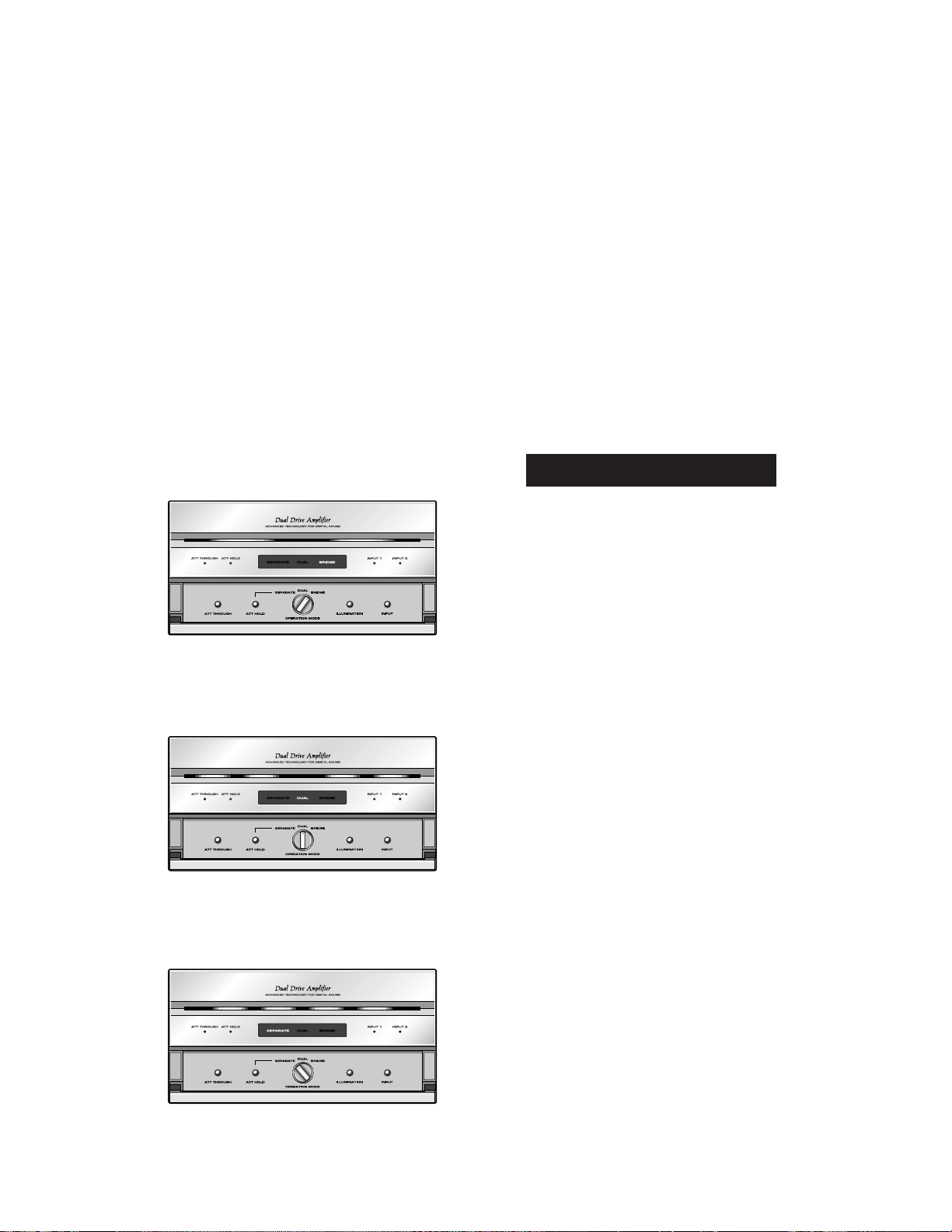
M-AX10
6 INPUT
This button allows you to switch between INPUT 1 and
INPUT 2. Note,however,that this is not possible if the
the OPERATION MODE switch is set to SEPARATE.
7 ATTENUATOR
This Knob allows you to adjust the attenuation in 31
stages.In dual and bridge modes it functions as a volume
control : 0 dB when turned full right, and - ∞ when turned
full left. In Separate mode it functions as an attenuator
for adjusting the volume of the high-frequncy channel
(0 to -15 dB,in 0.5 dB steps): turning it to the left lowers
the volume.
8 MODE ILLUMINATION LIGHT
The lamp display changes as illustrated below depending
on whether the OPERATION MODE switch is set to
BRIDEGE, DUAL or SEPARATE. Switching operations
modes while the power is on will activate the warning
circuit and cause the mode illumination light to flash.
Bridge mode
9 MODE INDICATOR
The lettering lights up to show whether the OPERATION
MODE switch is pointing to BRIDGE, DUAL ,SEPARATE.
Switching operation modes while the power is on will
activate the warning circuit and cause the mode indicator
to flash.
0 ATT THROUGH INDICATOR
This indicator lights up when ATT THROUGH is ON.
- ATT HOLD INDICATOR
This indicator lights up when ATT HOLD is ON.
= INPUT INDICATORS
These indicators light up to show whether INPUT 1 or
INPUT 2 has been selected. They both light up in Separate mode.
~ PANEL LIGHT
This illuminates the display panel.
METHODS OF CONNECTION
The M-AX10 has four built-in amplifier channels, which can
be connected by means of three different operation modes:
BRIDGE ,DUAL and SEPARATE. You may select the mode
which best suits your purpose and the equipment you are connecting to your M-AX10.
Dual mode
Separate mode
Bridge conection
• The four channels are connected two by two, so as to
act as two high-output amplifier channels.
• Output comprises two 230 W/ 6 Ω (DIN),200 W/ 6 Ω (FTC)
channels.
• Your speakers must be at least 6 Ω .
Dual conection
• The four channels act as two parallel sets of twin amplifier
channels.
• Output comprises two 110 W/ 3 Ω (DIN),90 W/ 3 Ω (FTC)
channels.
• Speakers with bi-wire terminals will allow you to achieve
high-quality sound.
Separate conection
• The channels act separately as four amplifier channels.
• Output comprises two 110 W/ 3 Ω (DIN),90 W/ 3 Ω (FTC)
channels.
• Connecting a channel divider will allow you to use the
appliance as an amplifier for a multi-channel system.
• You can adjust the volume of speakers connected to the
HIGH channels (INPUT 1) in a range from 0 to 15 dB.
You can also retain the attenuation once you have set it.
• Speakers connected to the LOW channels (INPUT 2) will
always be at maximum volume.
59
Page 60

M-AX10
REAR SECTION
INPUT 2
This is an input terminal for connecting
CD players,control amplifiers,channel
dividers and other components.
SPEAKERS (R)
These are terminal for right-hand
speakers.
Earth
This is used for an earth
connection with a source
appearance equipped with an
earth-floating function.
INPUT 1
This is an input terminal for
connecting CD players,control
amplifiers,channel dividers and
other components.
SPEAKERS (L)
These are terminal for
left-hand speakers.
60
BEWARE
When connecting,make sure that the
power switch is off,and the power cord
is disconnected from the power supply.
The terminals are arranged symmetrically.
Special care is required when connecting
the speaker cords:
failure to connect them in the correct
manner for the desired mode will result
in lost or imperfect sound.
The rear and under sections of this appliance
are copper plated to ensure high quality sound.
It may somtimes happen that marks are left
during the plating process,but this does not
affect performance.
Page 61

SPECIFICATIONS
Amplifier Section
(U.S model only)
When set to Bridge mode:
Continuous average power output is 200 Watts* per
channel, min.,at 6 ohms from 20 Herz to 20,000 Herz
with no more than 0.2%** total harmonic distortion.
When set to Dual mode ,Seaprate mode:
Continuous average power output is 90 Watts* per
channel, min.,at 3 ohms from 20 Herz to 20,000 Herz
with no more than 0.2%** total harmonic distortion.
Continuous power output
(driven simultaneously at 20Hz to 20kHz) **
(European mode only)
Bridge mode
T.H.D. 0.15% 6 Ω .................................................................... 220W × 2
T.H.D. 0.09% 8 Ω .................................................................... 190W × 2
Dual, Seaprate mode
T.H.D. 0.15% 3 Ω .................................................................... 100W × 4
T.H.D. 0.09% 4 Ω ...................................................................... 90W × 4
T.H.D. 0.08% 8 Ω ...................................................................... 60W × 4
DIN Continuous power output
(driven simultaneously at 1kHz)
(European mode only)
Bridge mode
T.H.D. 1% 6 Ω .......................................................................... 230W × 2
T.H.D. 1% 8 Ω .......................................................................... 200W × 2
Dual, Seaprate mode
T.H.D. 1% 3 Ω .......................................................................... 110W × 4
T.H.D. 1% 4 Ω .......................................................................... 105W × 4
T.H.D. 1% 8 Ω ............................................................................ 65W × 4
Total harmonic distortion **
Bridge mode
20 Hz to 20 kHz,100W, 8Ω ..........................................................0.08%
Dual, Seaprate mode
20 Hz to 20 kHz,30W, 8Ω.............................................................0.06%
M-AX10
Signal-to Noise ratio (IHF short circuit, A network
ATT THROUGH ON)
INPUT 1,2 .............................................................................. 125dB
Channel separation(20Hz to 20 kHz)
Bridge mode........................................................................... 104dB
Dual, Seaprate mode .............................................................115dB
Power supply/Mischellaneouse
Power requirements
U.S.model ................................................................. AC120V 60Hz
European model................................................... AC230V 50/60Hz
Power comsumption
U.S.model ............................................................................... 370W
European model...................................................................... 400W
Dimensions ................................... 440 (W) × 420 (D) × 178 (H) mm
175/16 (W) × 161/2 (D) × 7 (H)in.)
Weight (without package) ..............................25.8 kg (56 lbs 14oz)
Accessories
Operation instructions .................................................................... 1
Warranty card ................................................................................ 1
NOTE
Specifications and design subject to possible modifications
without notice ,due to improvement.
* Mesured pursuant to the Federal Trade Commissions' Trade
Regulation rule on Power Claims for Amplifier.
** Mesured by Audio Spectrum Analyzer.
Input sensitivity/Impedance
INPUT 1,2 .......................................................................... 1V/47kΩ
Frequency Response
INPUT 1,2 ............................................ 5Hz to 150 kHz +0dB, -3dB
Damping factor (1kHz/20Hz to 20kHz)
............................................................................................ 400/300
61
 Loading...