

Page 1
PIONEER CORPORATION 4-1, Meguro 1-Chome, Meguro-ku, Tokyo 153-8654, Japan
PIONEER ELECTRONICS SERVICE INC. P.O.Box 1760, Long Beach, CA 90801-1760 U.S.A.
PIONEER EUROPE NV Haven 1087 Keetberglaan 1, 9120 Melsele, Belgium
PIONEER ELECTRONICS ASIACENTRE PTE.LTD. 253 Alexandra Road, #04-01, Singapore 159936
C PIONEER CORPORATION 2000
K-ZZD. OCT. 2000 Printed in Japan
ORDER NO.
CRT2582
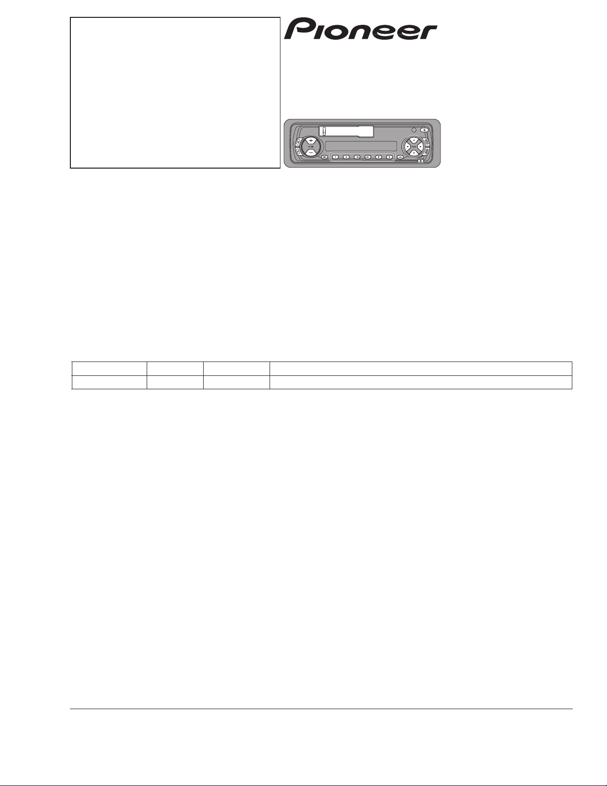
MULTI-CD CONTROL HIGH POWER CASSETTE PLAYER WITH RDS TUNER
KEH-P4010R X1M/EW
CONTENTS
1. SAFETY INFORMATION ............................................2
2. EXPLODED VIEWS AND PARTS LIST.......................2
3. BLOCK DIAGRAM AND SCHEMATIC DIAGRAM.....9
4. PCB CONNECTION DIAGRAM ................................20
5. ELECTRICAL PARTS LIST ........................................28
6. ADJUSTMENT..........................................................32
7. GENERAL INFORMATION .......................................33
7.1 DIAGNOSIS ........................................................33
7.1.1 DISASSEMBLY .........................................33
7.1.2 CONNECTOR FUNCTION DESCRIPTION34
7.2 PARTS .................................................................35
7.2.1 IC................................................................35
7.2.2 DISPLAY....................................................40
7.3 OPERATIONAL FLOW CHART ...........................41
8. OPERATIONS AND SPECIFICATIONS.....................42
KEH-P4010R/X1M/EW
- This service manual should be used together with the following manual(s):
Model No. Order No. Mech. Module Remarks
CX-1011 CRT2406 3L Cassette Mech. Module:Mech.Description, Disassembly, Adjustment
- This service manual does not describe the CD test mode.
For the operations in the CD test mode, refer to the CD player's Service manual.
KEH-P4010RB X1M/EW
KEH-P4013R X1M/EW
Page 2
2
KEH-P4010R,P4010RB,P4013R
1. SAFETY INFORMATION
This service manual is intended for qualified service technicians; it is not meant for the casual do-it-yourselfer.
Qualified technicians have the necessary test equipment and tools, and have been trained to properly and safely repair
complex products such as those covered by this manual.
Improperly performed repairs can adversely affect the safety and reliability of the product and may void the warranty.
If you are not qualified to perform the repair of this product properly and safely, you should not risk trying to do so
and refer the repair to a qualified service technician.
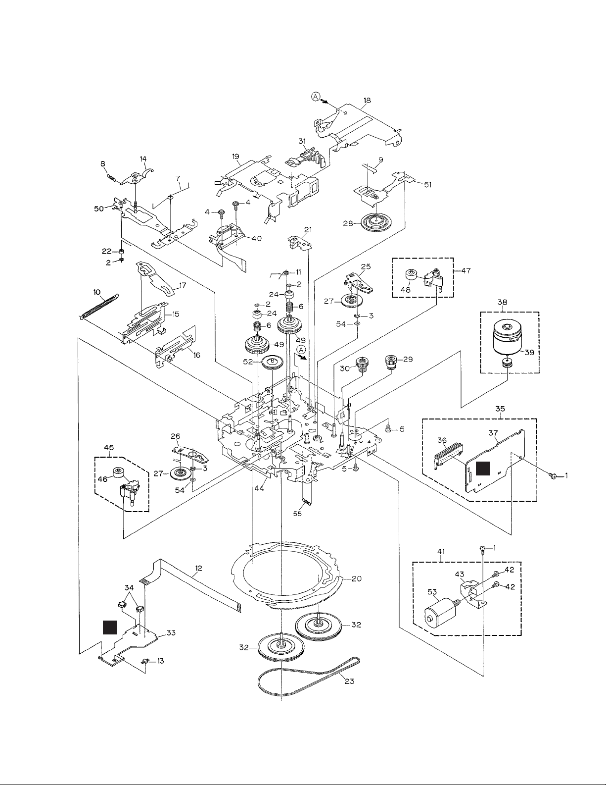
2. EXPLODED VIEWS AND PARTS LIST
2.1 PACKING
10
1
13
7
11
9
8
2
5
4
6
3
12
Page 3
3
KEH-P4010R,P4010RB,P4013R
1 Cord Assy CDE6514
2 Accessory Assy CEA1917
3 Screw CBA1304
4 Handle CNC5395
5 Bush CNV3930
* 6 Polyethylene Bag E36-615
7 Polyethylene Bag CEG-162
8 Carton
See Contrast table(2)
9 Contain Box See Contrast table(2)
10 Protector CHP2346
11 Protector CHP2347
12-1 Owner’s Manual CRD3286
12-2 Owner’s Manual CRD3287
12-3 Installation Manual CRD3293
* 12-4 Passport CRY1013
* 12-5 Warranty Card CRY1157
* 12-6 Caution Card CRP1238
13 Case Assy CXB3520
Mark No. Description Part No. Mark No. Description Part No.
(1) PACKING SECTION PARTS LIST
NOTE:
- Parts marked by “*” are generally unavailable because they are not in our Master Spare Parts List.
- Screws adjacent to ∇ mark on the product are used for disassembly.
- Owner's Manual, Installation Manual
Model Part No. Language
KEH-P4010R/X1M/EW CRD3286 English, Spanish, German
KEH-P4013R/X1M/EW CRD3287 French, Italian, Dutch
KEH-P4010RB/X1M/EW CRD3293 English, Spanish, German,
French, Italian, Dutch
Part No.
Mark No. Symbol and Description KEH-P4010R/X1M/EW KEH-P4013R/X1M/EW KEH-P4010RB/X1M/EW
8 Carton CHG4183 CHG4185 CHG4184
9 Contain Box CHL4183 CHL4185 CHL4184
(2) CONTRAST TABLE
KEH-P4010R/X1M/EW, KEH-P4013R/X1M/EW and KEH-P4010RB/X1M/EW are constructed the same
except for the following:
Page 4
4
KEH-P4010R,P4010RB,P4013R
2.2 EXTERIOR
A
B
Page 5

5
KEH-P4010R,P4010RB,P4013R
1 Screw BSZ26P050FMC
2 Screw BSZ30P050FMC
3 Screw BSZ30P200FMC
4 Cord Assy CDE6514
5 Fuse(10A) CEK1136
6 Case CNB2350
7 Holder CNC5704
8 Cushion CNM5210
9 Insulator CNM7083
10 Tuner Amp Unit
See Contrast table(2)
11 Screw BPZ26P080FMC
12 Screw BSZ26P080FMC
13 Screw BSZ26P160FMC
14 Cord CDE6450
15 FM/AM Tuner Unit CWE1562
16 Holder CNC8815
17 Pin Jack(CN301) CKB1035
18 Terminal(CN403) CKF1059
19 Plug(CN952) CKM1270
20 Connector(CN751) CKS3408
21 Connector(CN602) CKS3568
22 Connector(CN601) CKS3581
23 Antenna Jack(CN401) CKX1056
24 Panel CNB2341
25 Holder CNC6845
26 Holder CNC7996
27 Heat Sink CNR1505
28 Detach Grille Assy
See Contrast table(2)
29 Screw BPZ20P100FZK
30 Button(DETACH)
See Contrast table(2)
31 Button(1–6) CAC6822
32 Button(A,B) CAC6823
33 Button(EJECT, BSM) CAC6824
34 Button(CROSS) CAC6825
35 Button(+,-) CAC6834
36 Button(SOURCE) CAC6851
37 Spring CBH2210
38 Cover
See Contrast table(2)
39 Keyboard Unit See Contrast table(2)
40 LCD(LCD1902) See Contrast table(2)
41 Connector(CN1901) CKS3580
42 Holder CNC9091
43 •••••
44 Sheet CNM7059
45 Rubber CNV6480
46 Lighting Conductor CNV6495
47 Lighting Conductor CNV6496
48 Connector CNV6497
49 Grille Unit
See Contrast table(2)
50 Chassis Unit See Contrast table(2)
51 Holder Unit CXB6681
52 Button CAC4836
53 Spring CBH1834
54 Spring CBH1835
55 Spring CBH2182
56 Bracket CNC6135
57 Bracket CNC6791
58 Arm CNV4692
59 Arm CNV4693
60 Arm CNV4728
61 Panel Unit
See Contrast table(2)
62 Door See Contrast table(2)
63 Spring CBH1838
64 Screw IMS20P030FZK
65
Cassette Mechanism Module EXK4170
66 Screw ISS26P055FUC
67 IC(IC301) TA8277H
68 Transistor(Q951) 2SD2396
69 •••••
70 Terminal Cover CKX-003
71 Sheet
See Contrast table(2)
(1) EXTERIOR SECTION PARTS LIST
Mark No. Description Part No. Mark No. Description Part No.
Page 6

6
KEH-P4010R,P4010RB,P4013R
Part No.
Mark No. Symbol and Description KEH-P4010R/X1M/EW KEH-P4013R/X1M/EW KEH-P4010RB/X1M/EW
10 Tuner Amp Unit CWM7331 CWM7332 CWM7333
28 Detach Grille Assy CXB6176 CXB6177 CXB6178
30 Button CAC5789 CAC5929 CAC5789
38 Cover CNS6171 CNS6172 CNS6171
39 Keyboard Unit CWM7343 CWM7344 CWM7345
40 LCD(LCD1902) CAW1634 CAW1634 CAW1618
49 Grille Unit CXB6711 CXB6333 CXB6712
50 Chassis Unit CXB6663 CXB6664 CXB6665
61 Panel Unit CXB6715 CXB6716 CXB6715
62 Door CAT2109 CAT2108 CAT2109
71 Sheet Not used Not used CNM7157
(2) CONTRAST TABLE
KEH-P4010R/X1M/EW, KEH-P4013R/X1M/EW and KEH-P4010RB/X1M/EW are constructed the same
except for the following:
Page 7
7
KEH-P4010R,P4010RB,P4013R
2.3 CASSETTE MECHANISM MODULE
C
D
Page 8

8
KEH-P4010R,P4010RB,P4013R
1 Screw BSZ20P040FMC
2 Washer CBF1037
3 Washer CBG1003
4 Screw EBA1028
5 Screw CBA1037
6 Spring EBH1531
7 Spring EBH1642
8 Spring EBH1641
9 Spring EBH1626
10 Spring EBH1627
11 Spring EBH1649
12 Cord EDD1024
13 Photo-reflector(EGN1) EGN1004
14 Arm ENC1526
15 Lever ENC1544
16 Lever ENC1543
17 Arm ENC1532
18 Frame ENC1533
19 Holder ENC1534
20 Gear ENC1535
21 Arm ENC1550
22 Roller ENR1040
23 Belt ENT1027
24 Collar ENV1508
25 Arm ENV1539
26 Arm ENV1540
27 Gear ENV1544
28 Gear ENV1547
29 Gear ENV1560
30 Worm Wheel ENV1566
31 Lever ENV1551
32 Flywheel ENV1554
33 Gathering PCB ENX1068
34 Switch(S1,S2) ESG1007
* 35 Deck Unit EWM1032
36 Plug(CN251) CKS3540
37 Gathering PCB ENX1067
38 Motor Unit(M1) EXA1491
39 Motor EXM1028
40 Head Assy(HD1) EXA1592
41 Motor Unit(M2) EXA1580
42 Screw BMZ20P022FMC
43 Bracket ENC1528
44 Chassis Unit EXA1615
45 Pinch Holder Unit EXA1608
46 Pinch Roller ENV1518
47 Pinch Holder Unit EXA1607
48 Pinch Roller ENV1518
49 Reel Unit EXA1585
50 Head Base Unit EXA1611
51 Lever Unit EXA1587
52 Gear Unit EXA1596
53 Motor Unit(Service) EXX1055
54 Washer HBF-179
55 Spring EBH1537
Mark No. Description Part No. Mark No. Description Part No.
- CASSETTE MECHANISM MODULE SECTION PARTS LIST
Page 9
9
KEH-P4010R,P4010RB,P4013R
1
2
34
1
2
34
D
C
B
A
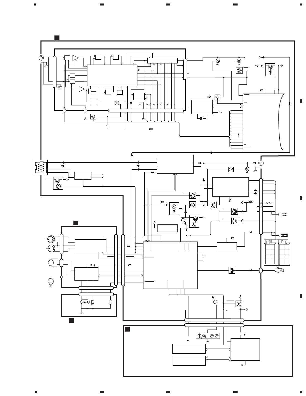
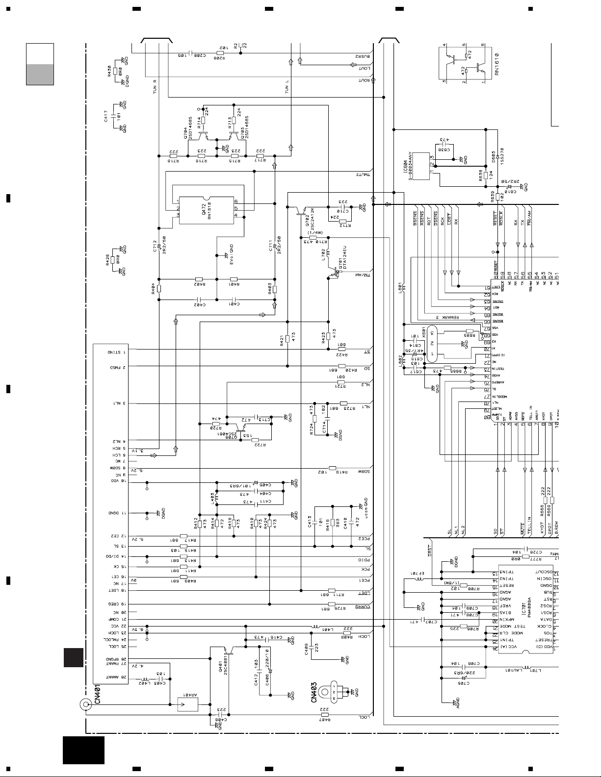
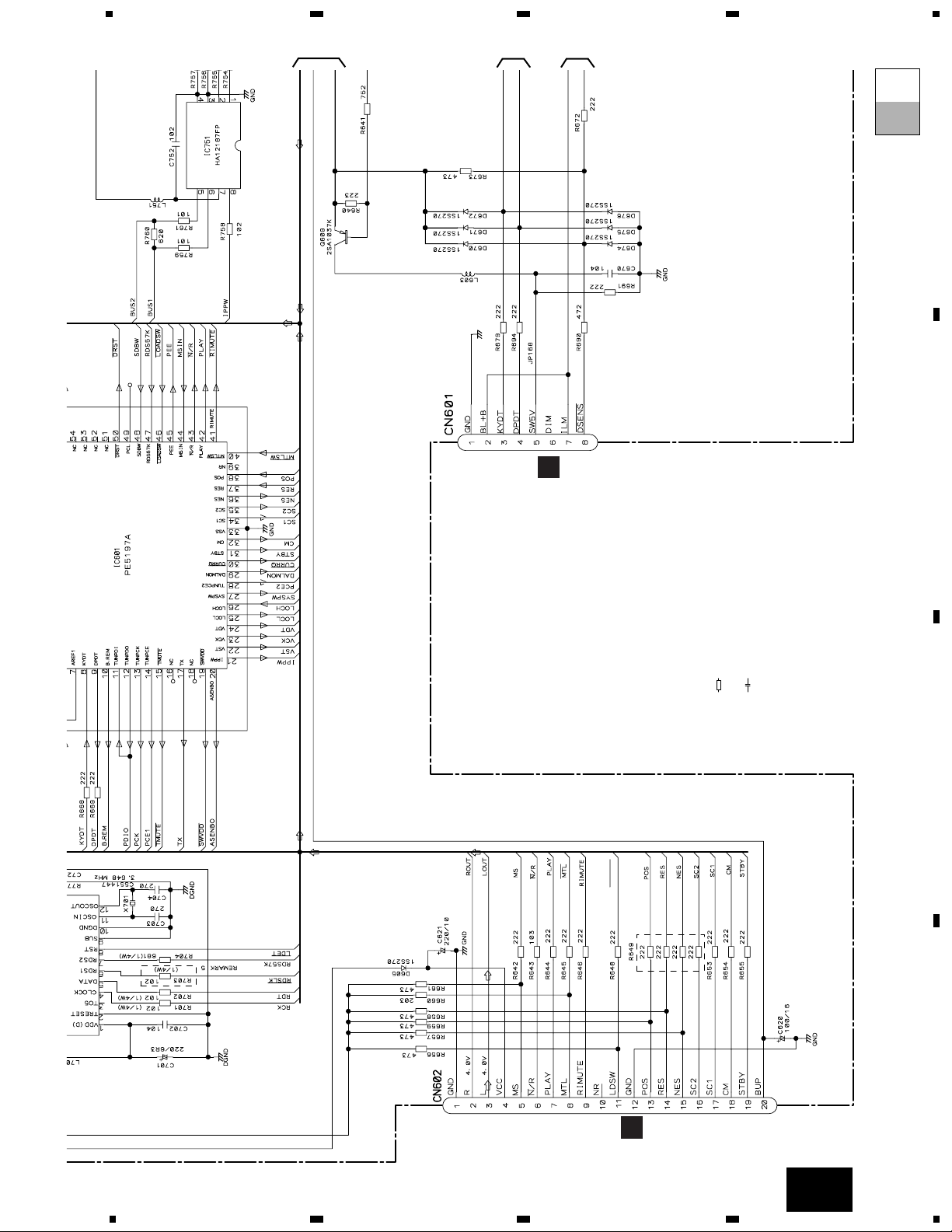
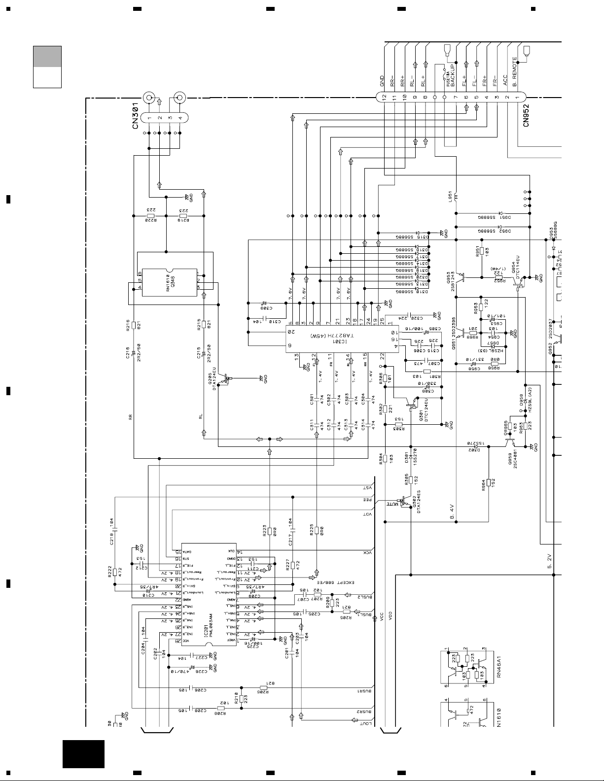
3. BLOCK DIAGRAM AND SCHEMATIC DIAGRAM
3.1 BLOCK DIAGRAM
TUNER Lch
Q702
Q472
Q703
LDET
TMUTE
B.U
VDD
Q952
SYSPW
TMUTE
SYSPW
VDD
AVDD
61
27 74
68
SYSTEM
CONTROLLER
PE5197A
IC601(1/2)
TUN-L
TUN-L
ELECTRONIC VOLUME
PML003AM
IC201
11
10
2
4
TAPE-L
RL
FL
POWER AMP
IC301
12
14
MUTE
STBY
FL
RL
FL+
FL-
RL+
RL-
22 4
9
7
19
17
SYSPW
B.U
B.U
SYSPW
Q302
Q951
Q959
Q301
Q953
Q601
Q602
MUTE
8.4V
REGULATOR
RESET
IC604
S-80834ANY
VCC
VDD
560
1
2
66 65
70
69
6
41
31
MUTE
RESET
BSENS
ASENS
SWVDD
DPDT
KYDT
DSENS
RIMUTE
STBY
LOADSW
X1
X2
TELIN
SYSTEM
CONTROLLER
IC601(2/2)
PE5197A
X601
Q954
BSENS
ASENS
ACC
FUSE
10A
TEL MUTE
Q611
B.U
STBY
B.U
MUTE
LOAD
46
63
8
9
19
Q650
SWVDD
VDD
SW5V
ILL
KYDT
DPDT
SW5V
VDD SWITCH
5
1
4
2
1
3
4
11
9
20
19
3
4
11
9
20
19
9
6
2
1
5
8
7
A
TUNER AMP UNIT
C
DECK UNIT
B
KEYBOARD UNIT
734 5
734 5
LCD DRIVER
IC1901
PD6293A
DPDT
KYDT
VDD
VLCD
XO
XI
X901
18
20
56
10
22
23
IC251
HA12229F
IC351
PA2020A
EQ AMP
MECHANISM
DRIVER
CN251
CN252
CN254
CN255
CN253
6
15
TAPE+B
Lch
20
FWD
L-ch
REV
L-ch
39
32
33
18
19
17
3
15 6
8
7
10
CN256
3
15 6
S1
LOAD
S2
MODE
EGN1
REEL
SENSE
M
M
M2
SUB
MOTOR
M1
MAIN
MOTOR
5
2
1
D
REEL SENSE PCB
CN602
CN952
CN901
CN601
CN1901
VCK/VDT/VST
ACC
BACK UP
FL+
FL-
RLRL+
TEL MUTE
B.REMOTE
VCC
LOUT
RIMUTE
LDSW
STBY
KEY MATRIX
LCD
IC 3
EEPROM
ANTENNA
JACK
1
2
FM/AM TUNER UNIT
28
27
FM/AM 1ST IF 10.7MHz
T51 Q51 CF51
CF52 CF53
IC1
MIXER, IF AMP, DET.
6
21
18
LDET
COMP
222510 14 12 15 16 8 13 2 3 4
CF202
VDD
LOCL
VCC
Q401
VCC
VDD
DI/DO
CE2CKCE1
SDBWSLFMSD
PCE2
TUNPCK
TUNPCE
SDBW
SL
SD
PDIO
NL1
NL2
IC 2 FM MPX
NL1
LDET
15
RDS
DECODER
IC 701
PM4009A
20
11 12
24
X702
Q701
VDD
FM/AM
FM/AM
55
78
NL1
SD
SL
SDBW
TUNPCE
TUNPCK
TUNPCE2
TUNPDO
LOCL
1
76
48
14
13
28
12
25
TUNPDI
11
PDIO
SWVDD
POWER SWITCH
1
6
IC602
TPD1018F
8
8
DSENS
A
A
AMANT
FMANT
ATT
ATT
AMRF
FMRF
IMG ADJ
RF ADJ
X901
10.25MHz
ANTSW
LOCL
23
LOCH
AMDET
MPXREF 41kHz
AM 2ND IF
450kHz
19
CREQCURRQ
11
DGND
DGND
1
STIND
ST
L ch
ST
2
CURRQ
30
TA8277H
1
2
8
5
6
B.U
TX
RX
IPPW
ASENBO
IP-BUS DRIVER
IC751
HA12187FP
BUSL1
BUSL2
BUS2
BUS1
Q751
Q752
8
1
5
11
7
CN751
IP-BUS
BUSL1
5
BUSL2
6
1
2
CN301
Q346
Q205
MUTE
TX
RX
17
61
20
ASEMBO
IPPW
21
RR
+
RR
FR
+
FR
FL
+
FL
RL
+
RL
-
ACC
GND
B.
REM
BACK
UP
LOCH
LOCH
26
CN401
REAR OUTPUT
L
5
R ch
924
NC
FMLOCL
20177
NCNCWC
26
RFGND
NL2
79
NL2DT
NL2
9
PEE
45
PEE
B.REM
10
B.U
5
Page 10
10
KEH-P4010R,P4010RB,P4013R
1
23
4
1234
D
C
B
A
3.3 OVERALL CONNECTION DIAGRAM(GUIDE PAGE)
Note: When ordering service parts, be sure to refer to “EXPLODED VIEWS AND PARTS LIST” or “ELECTRICAL PARTS
LIST”.
A-a A-b
A-aA-a
A-b A-b
A-b A-b
A-a A-a
Large size
SCH diagram
Guide page
Detailed page
A
A-a
B
C
DSP-201M-S00B
X601:CSS1310
6.29MHz
0R0
162
162
272
272
123123
FM/AM TUNER UNIT
ANTENNA JACK
A
CN1901
CN251
For resistors and capacitors in the circuit diagrams, their resistance values or
capacitance values are expressed in codes:
Ex. *Resistors
Code Practical value
123 12k ohms
103 10k ohms
*Capacitors
Code Practical value
103 0.01uF
101/10 100uF/10V
TUNER AMP UNIT
LOADSW
The > mark found on some component parts indicates
the importance of the safety factor of the part.
Therefore, when replacing, be sure to use parts of
identical designation.
Symbol indicates a resistor.
No differentiation is made between chip resistors and
discrete resistors.
NOTE :
Symbol indicates a capacitor.
No differentiation is made between chip capacitors and
discrete capacitors.
SYSTEM CONTROLLER
SWD 5V
B
FM(100%) 400Hz
AM(30%) 400Hz
: -15.5dBs
: -26.0dBs
TAPE (0dB)315Hz : -9.9dBs
IP-BUS DRIV
Page 11
11
KEH-P4010R,P4010RB,P4013R
5
6
78
5
6
78
D
C
B
A
A-b
A
600µH
332/16
>CEK1136
RR
+
RR
FR
+
FR
FL
+
FL
RL
+
RL
-
ACC
GND
B.
REM
BACK
UP
REAR OUTPUT
L
R
111098
765
4321
IP-BUS INPUT
SOURCE SELECTOR,
ELECTRONIC VOLUME
MUTE
POWER AMP
8.4V REGULATOR
OFF MUTE
5V REGULATOR
POWER SWITCH
BACK UP SENSE
ACC SENSE
CELLULAR MUTE
SYSTEM MUTE
IP-BUS(0dB)1kHz : 2.2dBs
TAPE : -4.6dBs
TAPE : 22.2dBs
FM
AM
IP-BUS
TAPE
: 6.6dBs
: -2.9dBs
: 10.3dBs
: -3.8dBs
Page 12
12
KEH-P4010R,P4010RB,P4013R
1
23
4
1234
D
C
B
A
DSP-201M-S00B
X601:CSS1310
6.29MHz
0R0
162
162
272
272
123123
FM/AM TUNER UNIT
ANTENNA JACK
A
TUNER AMP UNIT
SYSTEM CONTROLLER
FM(100%) 400Hz
AM(30%) 400Hz
: -15.5dBs
: -26.0dBs
A-a
A-a
A-b
1
2
3
Page 13
13
KEH-P4010R,P4010RB,P4013R
5
6
78
5
6
78
D
C
B
A
B
C
CN1901
CN251
For resistors and capacitors in the circuit diagrams, their resistance values or
capacitance values are expressed in codes:
Ex. *Resistors
Code Practical value
123 12k ohms
103 10k ohms
*Capacitors
Code Practical value
103 0.01uF
101/10 100uF/10V
LOADSW
The > mark found on some component parts indicates
the importance of the safety factor of the part.
Therefore, when replacing, be sure to use parts of
identical designation.
Symbol indicates a resistor.
No differentiation is made between chip resistors and
discrete resistors.
NOTE :
Symbol indicates a capacitor.
No differentiation is made between chip capacitors and
discrete capacitors.
SYSTEM CONTROLLER
SWD 5V
BACK L
TAPE (0dB)315Hz : -9.9dBs
IP-BUS DRIVER
A-a
A-a
A-b
4
5
6
7
Page 14
14
1
23
4
1234
D
C
B
A
600µH
332/16
>CEK1136
REAR OUTPUT
L
R
SOURCE SELECTOR,
ELECTRONIC VOLUME
MUTE
POWER AMP
8.4V REGULATOR
OFF MUTE
5V REGULATOR
SYSTEM MUTE
TAPE : -4.6dBs
TAPE : 22.2dBs
FMAMIP-BUS
TAPE
: 6.6dBs
: -2.9dBs
: 10.3dBs
: -3.8dBs
A-a
A-b
A-b
1
2
3
4
KEH-P4010R,P4010RB,P4013R
Page 15

15
5
6
78
5
6
78
D
C
B
A
RR
+
RR
-
FR
+
FR
-
FL
+
FL
-
RL
+
RL
-
ACC
GND
B.
REM
BACK
UP
111098
765
4321
IP-BUS INPUT
5V REGULATOR
POWER SWITCH
BACK UP SENSE
ACC SENSE
CELLULAR MUTE
IP-BUS(0dB)1kHz : 2.2dBs
A-b
A-a
A-b
4
5
6
7
KEH-P4010R,P4010RB,P4013R
Page 16

16
KEH-P4010R,P4010RB,P4013R
1
23
4
1234
D
C
B
A
4.97MHz
LCD DRIVER,
KEY CONTROLLER
EQ
PTY
B
3.3 KEYBOARD UNIT
Page 17

17
KEH-P4010R,P4010RB,P4013R
5
6
78
5
6
78
D
C
B
A
0R0
IL1801,1802 : 14V 40mA
A
CN601
B
KEYBOARD UNIT
KEH-P4010R/X1M/EW
SML210PT
CEL1651
CAW1634
151
D1811-1818
IL1801,1802
LCD1902
R1810,1813,1816
KEH-P4013R/X1M/EW
SML210DT
CEL1638
CAW1634
181
KEH-P4010RB/X1M/EW
SML210VT
CEL1662
CAW1618
181
EQ
LOCAL/BSM
TA
B
Page 18

18
KEH-P4010R,P4010RB,P4013R
1
23
4
1234
D
C
B
A
DECK UNIT
MUTE
HA12229F
11
12
13
14
15
16
17
18
19
20
40
39
38
37
36
35
34
33
32
31
30
292827
26
252423
22
21
1
234
5
678
9
10
C253
390P
C251
C256
R01
C405
R033
R404
270K
R01
C404
910
R403
3R3K
C255
R01
C272
R1
C401
3900P
R285 0R0
HD1
HEAD ASSY
EXA1592
TEST TAPE
NCT-150
(400Hz, 200nWb/m)
RL
RR
FR
FL
C302
R1
C301
R1
R304
R302
16K
16K
R301
16K
R303
16K
-8.24dBs±4dB
Fwd-R
Fwd-L
Rev-R
Rev-L
NF1(R)
Vref1
RIN(L)
NC
RIN(R)
GND
FIN(R)
Vref2
FIN(L)
NFI(L)
M-OUT(L)
EQOUT(L)
Vref4
TAI(L)
BIAS
NC
NC
MSGV(S)
MUTE
120/70
ser/REP
f/R
MSDET
MSI
MAOUT
MSGV(R)
MOUT(R)
EQOUT(R)
Vref3
TAI(R)
RIP
PBOUT(R)
NC
NC
NC
CN252
CN251
EQ AMP
IC251
390P
C252
390P
C254
390P
PBOUT(L)
NC
VCC
MSOUT
NC
C403
R022
R402
R33
C402
15K
R401
18K
R271
C271
1/50
3.4 CASSETTE MECHANISM MODULE
C
C
Decimal points for resistor
and capacitor fixed values
are expressed as :
2.2 2R2
0.022 R022
←
←
Symbol indicates a resistor.
No differentiation is made between chip resistors and
discrete resistors.
NOTE :
Symbol indicates a capacitor.
No differentiation is made between chip capacitors and
discrete capacitors.
Page 19

19
KEH-P4010R,P4010RB,P4013R
5
6
78
5
6
78
D
C
B
A
REEL SENSE
PCB
SWITCHES:
REEL SENSE PCB
S1:LOAD SWITCH..........EJECT-PLAY
S2:MODE SWITCH............ON-OFF
The underlined indicates the switch position.
R351 1K
R352 1K
R353 1K
R354 1K
R373 0R0
R355 270K
C352
3900P
R362 300
C351 R22
C353 R01
C354 R01
R374 0R0
C356 R01
C355 R1
D352 1SS355
M1 MOTOR UNIT
(MAIN MOTOR)
EXA1491
S1 LOAD
ESG1007
S2
ESG1007
MODE
REEL SENSE
EGN1
EGN1004
M2
MOTOR UNIT
(SUB MOTOR)
EXA1580
RS3
RS2
RS1
SC2
SC1
TAB
MC
CE
VCC2
NC
VCC
MCS
RRS
FRS
RSB
C
TAB
MS2
NC
NC
MM
SM1
RSB
GND
RS
mtl
MCS
load
CN255
CN253
CN256
CN254
MECHANISM
DRIVER
IC351 PA2020A
R022
C D
D
Page 20

20
KEH-P4010R,P4010RB,P4013R
1
23
4
1234
D
C
B
A
A
TUNER AMP UNIT
CORD ASSY
B
CN1901
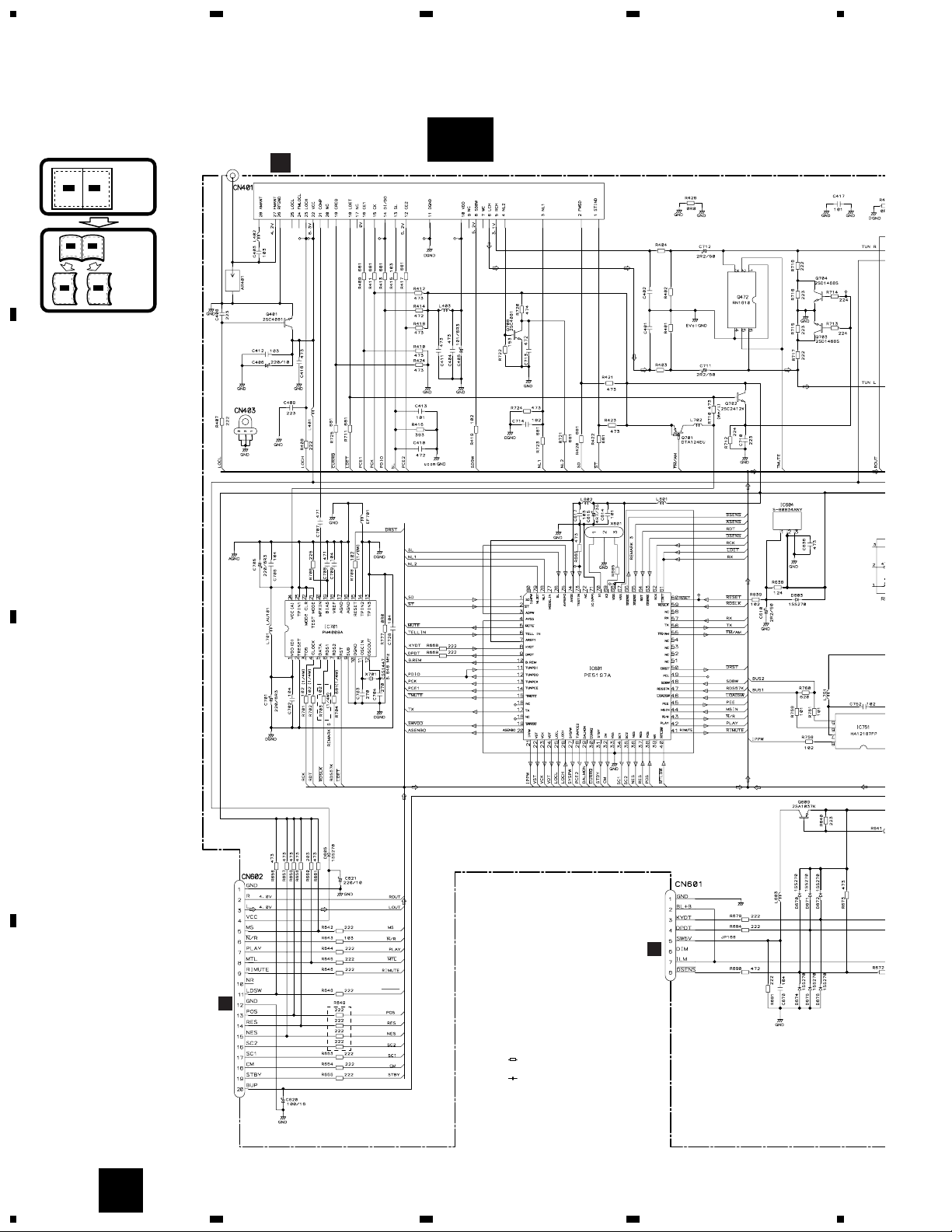
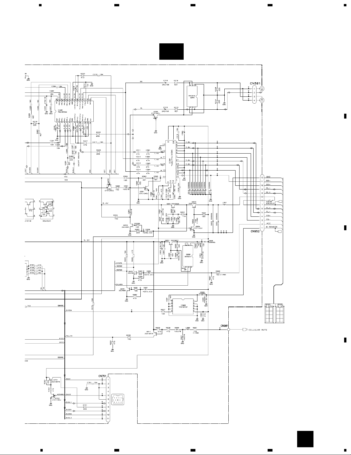
4. PCB CONNECTION DIAGRAM
4.1 TUNER AMP UNIT
NOTE FOR PCB DIAGRAMS
1. The parts mounted on this PCB
include all necessary parts for
several destination.
For further information for
respective destinations, be sure
to check with the schematic diagram.
2. Viewpoint of PCB diagrams
A
Capacitor
Connector
P.C.Board
Chip Part
SIDE A
SIDE B
Page 21

C
CN251
FM/AM TUNER UNIT
CORD
FRONT
REAR OUTPUT
IP-BUS INPUT
1
23
4
LR
ANTENNA
JACK
21
KEH-P4010R,P4010RB,P4013R
5
6
78
5
6
78
D
C
B
A
A
SIDE A
Page 22

22
KEH-P4010R,P4010RB,P4013R
1
23
4
1234
D
C
B
A
A
TUNER AMP UNIT
1
2
34
5
6
3
2
16
5
4
3
2
16
5
4
A
Page 23

23
KEH-P4010R,P4010RB,P4013R
5
6
78
5
6
78
D
C
B
A
A
SIDE B
Page 24

24
KEH-P4010R,P4010RB,P4013R
1
23
4
1234
D
C
B
A
4.2 KEYBOARD UNIT
B
KEYBOARD UNIT
EQ
VOL+
VOL-
SOURCE 1 2 3 4 5 6
LOCAL/BSM EJECT
AUDIO
BAND
←
↑
→
↑
B
SIDE A
PTY
TA
Page 25

B
KEYBOARD UNIT
A
CN601
25
KEH-P4010R,P4010RB,P4013R
1
2
34
1
2
34
D
C
B
A
B
SIDE B
Page 26

26
KEH-P4010R,P4010RB,P4013R
1
23
4
1234
D
C
B
A
CN251
CN271
IC,Q
IC251
Q351
Q352
ADJ
VR302
VR301
IC351
CN252
CN254
CN253
CN255
M1
M2
HEAD ASSY
CN256
21
22
4.4 CASSETTE MECHANISM MODULE
DECK UNIT
C
CN602
DECK UNIT
C
A
SIDE A
SIDE B
CN256
D
C
Page 27

27
KEH-P4010R,P4010RB,P4013R
1
2
34
1
2
34
D
C
B
A
1
2
3
4
5
6
S1
LOAD
S2
MODE
CN256
EGN1
REEL SENSE
REEL SENSE PCB
D
CN253
C
D
Page 28

28
KEH-P4010R,P4010RB,P4013R
5. ELECTRICAL PARTS LIST
NOTES:
- Parts whose parts numbers are omitted are subject to being not supplied.
- The part numbers shown below indicate chip components.
Chip Resistor
RS1/_S___J,RS1/__S___J
Chip Capacitor (except for CQS.....)
CKS....., CCS....., CSZS.....
=====Circuit Symbol and No.===Part Name Part No.
--- ------ ------------------------------------------ -------------------------
Unit Number : CWM7331(KEH-P4010R/X1M/EW)
Unit Number : CWM7332(KEH-P4013R/X1M/EW)
Unit Number : CWM7333(KEH-P4010RB/X1M/EW)
Unit Name : Tuner Amp Unit
MISCELLANEOUS
IC 201 IC PML003AM
IC 301 IC TA8277H
IC 601 IC PE5197A
IC 602 IC TPD1018F
IC 604 IC S-80834ANY
IC 701 IC PM4009A
IC 751 IC HA12187FP
Q 205 Transistor DTA124EU
Q 301 Transistor DTC124EU
Q 302 Transistor DTA124ES
Q 346 Transistor RN1610
Q 401 Transistor 2SC4081
Q 472 Transistor RN1610
Q 601 Transistor 2SC4081
Q 602 Transistor 2SC4081
Q 609 Transistor 2SA1037K
Q 611 Transistor 2SA1037K
Q 701 Transistor DTA124EU
Q 702 Transistor 2SC2412K
Q 703 Transistor 2SD1468S
Q 704 Transistor 2SD1468S
Q 708 Transistor 2SC4081
Q 751 Transistor 2SA1037K
Q 752 Transistor DTC114EU
Q 951 Transistor 2SD2396
Q 952 Transistor 2SD2037
Q 953 Transistor 2SB1243
Q 954 Transistor DTC114EU
Q 959 Transistor 2SC4081
Q 960 Transistor RN46A1
D 301 Diode 1SS270
D 302 Diode 1SS270
D 313 Diode S5688G
D 314 Diode S5688G
D 315 Diode S5688G
D 316 Diode S5688G
D 317 Diode S5688G
D 318 Diode S5688G
D 319 Diode S5688G
D 320 Diode S5688G
D 601 Diode HZS7L(C2)
D 602 Diode HZS7L(A1)
D 603 Diode 1SS270
D 605 Diode 1SS270
D 606 Diode 1SS270
D 607 Diode 1SS270
D 608 Diode S5688G
D 609 Diode S5688G
D 670 Diode 1SS270
D 671 Diode 1SS270
D 672 Diode 1SS270
D 674 Diode 1SS270
D 675 Diode 1SS270
D 676 Diode 1SS270
D 951 Diode S5688G
D 952 Diode S5688G
D 953 Diode S5688G
D 956 Diode HZS6L(B2)
D 957 Diode HZS9L(B3)
D 958 Diode HZS9L(A2)
L 401 Ferri-Inductor LAU1R0M
L 402 Ferri-Inductor LAU4R7K
L 403 Ferri-Inductor LAU1R0M
L 601 Ferri-Inductor LAU2R2K
L 602 Inductor LAU100K
L 603 Ferri-Inductor LAU2R2K
L 605 Ferri-Inductor LAU2R2K
L 701 Ferri-Inductor LAU101K
L 702 Inductor LAU100K
L 751 Ferri-Inductor LAU2R2K
L 951 Choke Coil 600µH CTH1168
X 601 Ceramic Resonator 6.29MHz CSS1310
X 701 Crystal Resonator 3.648MHz CSS1447
EF 701 Filter CTF1071
AR 401 Serge Protector DSP-201M-S00B
RESISTORS
R 205 RD1/4PU821J
R 206 RD1/4PU821J
R 207 RD1/4PU102J
R 208 RD1/4PU102J
R 209 RD1/4PU223J
R 210 RD1/4PU223J
R 215 RS1/16S821J
R 216 RD1/4PU821J
R 219 RS1/16S223J
R 220 RS1/16S223J
R 222 RS1/16S472J
R 223 RS1/16S0R0J
R 225 RS1/16S0R0J
R 227 RS1/16S472J
R 301 RS1/16S103J
R 302 RS1/16S221J
R 303 RS1/16S153J
R 304 RS1/16S103J
R 305 RS1/16S152J
R 306 RS1/16S101J
=====Circuit Symbol and No.===Part Name Part No.
--- ------ ------------------------------------------ -------------------------
A
Page 29

KEH-P4010R,P4010RB,P4013R
R 401 RS1/16S272J
R 402 RS1/16S272J
R 403 RS1/16S162J
R 404 RS1/16S162J
R 407 RD1/4PU222J
R 408 RD1/4PU222J
R 409 RS1/16S681J
R 410 RS1/16S473J
R 411 RS1/16S681J
R 412 RD1/4PU473J
R 413 RS1/16S681J
R 414 RD1/4PU472J
R 415 RS1/16S103J
R 416 RS1/16S393J
R 417 RD1/4PU681J
R 418 RS1/16S473J
R 419 RS1/16S102J
R 420 RS1/16S681J
R 421 RS1/16S473J
R 422 RS1/16S681J
R 423 RS1/16S473J
R 424 RS1/16S473J
R 425 RS1/16S0R0J
R 426 RS1/16S0R0J
R 430 RS1/16S0R0J
R 601 RS1/16S104J
R 602 RS1/16S473J
R 603 RS1/16S104J
R 604 RS1/16S223J
R 605 RS1/16S473J
R 606 RS1/16S473J
R 607 RS1/16S472J
R 608 RD1/4PU102J
R 627 RD1/4PU103J
R 628 RS1/16S472J
R 629 RS1/16S473J
R 630 RS1/16S102J
R 631 RD1/4PU153J
R 632 RS1/16S473J
R 638 RS1/16S124J
R 639 RD1/4PU102J
R 640 RS1/16S223J
R 641 RD1/4PU752J
R 642 RS1/16S222J
R 643 RD1/4PU103J
R 644 RD1/4PU222J
R 645 RS1/16S222J
R 646 RS1/16S222J
R 648 RD1/4PU222J
R 649 RAB4C222J
R 653 RS1/16S222J
R 654 RS1/16S222J
R 655 RS1/16S222J
R 656 RS1/16S473J
R 657 RS1/16S473J
R 658 RS1/16S473J
R 659 RS1/16S473J
R 660 RS1/16S203J
R 661 RS1/16S473J
R 665 RS1/16S473J
R 668 RS1/16S222J
R 669 RS1/16S222J
R 672 RS1/16S222J
R 673 RS1/16S473J
R 675 RS1/16S1R0J
R 679 RD1/4PU222J
R 685 RS1/16S0R0J
R 690 RD1/4PU472J
R 691 RS1/16S222J
R 694 RD1/4PU222J
R 701 RD1/4PU102J
R 702 RD1/4PU102J
R 703 RD1/4PU102J
R 704 RD1/4PU681J
R 706 RS1/16S225J
R 708 RS1/16S102J
R 710 RD1/4PU473J
R 711 RD1/4PU681J
R 712 RS1/16S224J
R 713 RS1/16S224J
R 714 RS1/16S224J
R 715 RS1/16S223J
R 716 RS1/16S223J
R 717 RS1/16S222J
R 718 RS1/16S222J
R 720 RS1/16S474J
R 721 RS1/16S681J
R 722 RS1/16S153J
R 723 RS1/16S681J
R 724 RS1/16S473J
R 751 RD1/4PU222J
R 752 RS1/16S223J
R 753 RS1/16S472J
R 754 RS1/16S102J
R 755 RS1/16S102J
R 756 RS1/16S473J
R 757 RS1/16S473J
R 758 RS1/16S102J
R 759 RD1/4PU101J
R 760 RS1/16S620J
R 761 RD1/4PU101J
R 777 RS1/16S0R0J
R 951 RS1/16S103J
R 952 RD1/4PU122J
R 953 RS1/16S122J
R 954 RS1/16S101J
R 955 RS1/16S183J
R 958 RS1/16S0R0J
R 963 RS1/16S223J
R 964 RD1/4PU152J
R 965 RS1/16S103J
R 967 RD1/4PU152J
R 968 RD1/4PU201J
CAPACITORS
C 201 CKSRYB104K16
C 202 CKSRYB104K16
C 203 CKSRYB104K16
C 204 CKSRYB104K16
C 205 CKSRYB105K6R3
C 206 CKSRYB105K6R3
C 207 CKSRYB105K6R3
C 208 CKSRYB105K6R3
C 209 CEJA4R7M35
C 210 CEJA4R7M35
C 211 CKSRYB153K25
C 212 CKSRYB153K25
C 215 CEJA2R2M50
C 216 CEJA2R2M50
C 217 CKSRYB104K16
=====Circuit Symbol and No.===Part Name Part No.
--- ------ ------------------------------------------ -------------------------
=====Circuit Symbol and No.===Part Name Part No.
--- ------ ------------------------------------------ -------------------------
29
Page 30

30
KEH-P4010R,P4010RB,P4013R
C 218 CKSRYB104K16
C 225 CEJA100M16
C 226 CEJA470M10
C 227 CKSRYB104K16
C 301 CKSQYB474K16
C 302 CKSQYB474K16
C 303 CKSQYB474K16
C 304 CKSQYB474K16
C 305 CEJA100M16
C 306 CKSQYB225K10
C 307 CKSRYB473K16
C 308 CEJA330M10
C 309 3300µF/16V CCH1368
C 310 CKSRYB104K16
C 311 CKSQYB474K16
C 312 CKSQYB474K16
C 313 CKSQYB474K16
C 314 CKSQYB474K16
C 315 CKSQYB225K10
C 320 CKSRYB224K16
C 401 CKSRYB123K25
C 402 CKSRYB123K25
C 403 CKSQYB103K50
C 404 CKSRYB473K16
C 405 CEJA101M6R3
C 406 CEJA220M10
C 408 CKSRYB223K25
C 409 CKSRYB223K25
C 410 CKSRYB472K50
C 411 CKSRYB473K16
C 412 CKSRYB103K50
C 413 CCSRCH101J50
C 416 CKSRYB473K16
C 417 CCSRCH101J50
C 601 CKSRYB103K50
C 602 CKSRYB472K50
C 610 CEJA2R2M50
C 614 CCSRCH101J50
C 615 CEJA4R7M35
C 617 CKSRYB103K50
C 620 CEJA100M16
C 621 CEJA220M10
C 636 CKSRYB473K16
C 670 CKSRYB104K16
C 701 CEJA220M6R3
C 702 CKSRYB104K16
C 703 CCSRCH270J50
C 704 CCSRCH270J50
C 705 CEJA220M6R3
C 706 CKSRYB104K16
C 707 CKSRYB471K50
C 708 CKSRYB471K50
C 709 CKSRYB104K16
C 710 CKSRYB223K25
C 711 CEJA2R2M50
C 712 CEJA2R2M50
C 713 CKSRYB472K50
C 714 CKSRYB182K50
C 728 CKSRYB104K16
C 751 CKSRYB104K16
C 752 CKSRYB102K50
C 951 470µF/16V CCH1183
C 952 CEJA470M10
C 953 100µF/16V CCH1179
C 954 CKSRYB103K50
C 956 CKSRYB103K50
C 957 CCSRCH101J50
C 958 330µF/10V CCH1181
Unit Number : CWM7343
(KEH-P4010R/X1M/EW)
Unit Name : Keyboard Unit
MISCELLANEOUS
IC 1901 IC PD6340A
D 1811 LED SML210PT
D 1812 LED SML210PT
D 1813 LED SML210PT
D 1814 LED SML210PT
D 1815 LED SML210PT
D 1816 LED SML210PT
D 1817 LED SML210PT
D 1818 LED SML210PT
D 1850 LED NSSW440-9159
D 1851 LED NSSW440-9159
D 1901 Diode MA152WK
D 1902 Diode MA152WA
X 1901 Ceramic Resonator 4.97MHz CSS1422
IL 1801 Lamp 14V 40mA CEL1651
IL 1802 Lamp 14V 40mA CEL1651
LCD1902 LCD CAW1634
RESISTORS
R 1809 RS1/16S131J
R 1810 RS1/16S151J
R 1811 RS1/16S181J
R 1812 RS1/16S181J
R 1813 RS1/16S151J
R 1814 RS1/16S181J
R 1815 RS1/16S181J
R 1816 RS1/16S151J
R 1817 RS1/16S181J
R 1818 RS1/16S181J
R 1823 RS1/16S471J
R 1824 RS1/16S471J
R 1825 RS1/16S471J
R 1826 RS1/16S471J
R 1850 RS1/16S151J
R 1851 RS1/16S151J
R 1852 RS1/16S151J
R 1853 RS1/16S0R0J
R 1901 RS1/10S222J
R 1902 RS1/10S222J
R 1905 RS1/16S473J
CAPACITORS
C 1810 CKSQYB104K16
C 1811 CKSQYB104K16
C 1902 CKSRYB103K50
Unit Number : CWM7344
(KEH-P4013R/X1M/EW)
Unit Name : Keyboard Unit
MISCELLANEOUS
IC 1901 IC PD6340A
D 1811 LED SML210DT
D 1812 LED SML210DT
D 1813 LED SML210DT
D 1814 LED SML210DT
D 1815 LED SML210DT
D 1816 LED SML210DT
D 1817 LED SML210DT
D 1818 LED SML210DT
D 1850 LED NSSW440-9159
=====Circuit Symbol and No.===Part Name Part No.
--- ------ ------------------------------------------ -------------------------
=====Circuit Symbol and No.===Part Name Part No.
--- ------ ------------------------------------------ -------------------------
B
B
Page 31

KEH-P4010R,P4010RB,P4013R
D 1851 LED NSSW440-9159
D 1901 Diode MA152WK
D 1902 Diode MA152WA
X 1901 Ceramic Resonator 4.97MHz CSS1422
IL 1801 Lamp 14V 40mA CEL1638
IL 1802 Lamp 14V 40mA CEL1638
LCD1902 LCD CAW1634
RESISTORS
R 1809 RS1/16S131J
R 1810 RS1/16S181J
R 1811 RS1/16S181J
R 1812 RS1/16S181J
R 1813 RS1/16S181J
R 1814 RS1/16S181J
R 1815 RS1/16S181J
R 1816 RS1/16S181J
R 1817 RS1/16S181J
R 1818 RS1/16S181J
R 1823 RS1/16S471J
R 1824 RS1/16S471J
R 1825 RS1/16S471J
R 1826 RS1/16S471J
R 1850 RS1/16S151J
R 1851 RS1/16S151J
R 1852 RS1/16S151J
R 1853 RS1/16S0R0J
R 1901 RS1/10S222J
R 1902 RS1/10S222J
R 1905 RS1/16S473J
CAPACITORS
C 1810 CKSQYB104K16
C 1811 CKSQYB104K16
C 1902 CKSRYB103K50
Unit Number : CWM7345
(KEH-P4010RB/X1M/EW)
Unit Name : Keyboard Unit
MISCELLANEOUS
IC 1901 IC PD6340A
D 1811 LED SML210VT
D 1812 LED SML210VT
D 1813 LED SML210VT
D 1814 LED SML210VT
D 1815 LED SML210VT
D 1816 LED SML210VT
D 1817 LED SML210VT
D 1818 LED SML210VT
D 1850 LED NSSW440-9159
D 1851 LED NSSW440-9159
D 1901 Diode MA152WK
D 1902 Diode MA152WA
X 1901 Ceramic Resonator 4.97MHz CSS1422
IL 1801 Lamp 14V 40mA CEL1662
IL 1802 Lamp 14V 40mA CEL1662
LCD1902 LCD CAW1618
RESISTORS
R 1809 RS1/16S131J
R 1810 RS1/16S181J
R 1811 RS1/16S181J
R 1812 RS1/16S181J
R 1813 RS1/16S181J
R 1814 RS1/16S181J
R 1815 RS1/16S181J
R 1816 RS1/16S181J
R 1817 RS1/16S181J
R 1818 RS1/16S181J
R 1823 RS1/16S471J
R 1824 RS1/16S471J
R 1825 RS1/16S471J
R 1826 RS1/16S471J
R 1850 RS1/16S151J
R 1851 RS1/16S151J
R 1852 RS1/16S151J
R 1853 RS1/16S0R0J
R 1901 RS1/10S222J
R 1902 RS1/10S222J
R 1905 RS1/16S473J
CAPACITORS
C 1810 CKSQYB104K16
C 1811 CKSQYB104K16
C 1902 CKSRYB103K50
Unit Number : EWM1032
Unit Name : Deck Unit
MISCELLANEOUS
IC 251 IC HA12229F
IC 351 IC PA2020A
D 352 Diode 1SS355
RESISTORS
R 271 RS1/16S183J
R 285 RS1/16S0R0J
R 301 RS1/16S163J
R 302 RS1/16S163J
R 303 RS1/16S163J
R 304 RS1/16S163J
R 351 RS1/16S102J
R 352 RS1/16S102J
R 353 RS1/16S102J
R 354 RS1/16S102J
R 355 RS1/16S274J
R 362 RS1/8S301J
R 373 RS1/16S0R0J
R 374 RS1/8S0R0J
R 401 RS1/16S153J
R 402 RS1/16S332J
R 403 RS1/16S911J
R 404 RS1/16S274J
CAPACITORS
C 251 CKSRYB391K50
C 252 CKSRYB391K50
C 253 CKSRYB391K50
C 254 CKSRYB391K50
C 255 CKSRYB103K50
C 256 CKSRYB103K50
C 271 1µF/50V ECH0002
C 272 CKSRYB104K16
C 301 CKSRYB104K16
C 302 CKSRYB104K16
C 351 CKSQYB224K25
C 352 CKSRYB392K50
C 353 CKSRYB103K50
C 354 CKSRYB103K50
C 355 CKSQYB104K50
=====Circuit Symbol and No.===Part Name Part No.
--- ------ ------------------------------------------ -------------------------
=====Circuit Symbol and No.===Part Name Part No.
--- ------ ------------------------------------------ -------------------------
31
BB
C
Page 32

32
KEH-P4010R,P4010RB,P4013R
C 356 CKSRYB103K50
C 401 CKSRYB392K50
C 402 CKSRYB334K10
C 403 CKSRYB223K25
C 404 CKSRYB103K50
C 405 CKSRYB333K16
Unit Number :
Unit Name : REEL SENSE PCB
S 1 Switch(LOAD) ESG1007
S 2 Switch(MODE) ESG1007
EGN 1 Photo-reflector EGN1004
Miscellaneous Parts List
M 1 Motor Unit(MAIN) EXA1491
M 2 Motor Unit(SUB) EXA1580
HD 1 Head Assy EXA1592
=====Circuit Symbol and No.===Part Name Part No.
--- ------ ------------------------------------------ -------------------------
D
6. ADJUSTMENT
There is no information to be shown in this chapter.
Page 33

33
KEH-P4010R,P4010RB,P4013R
- Removing the Tuner Amp Unit (Fig.2)
Remove the two screws.
Straight the tabs at four locations indicated.
Remove the screw.
Remove the three screws and then remove the
Tuner Amp Unit.
- Removing the Case (not shown)
1. Remove the two screws.
2. Remove the Case.
- Removing the Cassette Mechanism Module (Fig.1)
Remove the four screws and then remove the
Cassette Mechanism Module.
- Removing the Panel Assy (Fig.1)
Disconnect the two stoppers and then remove the
Panel Assy.
Fig.1
Fig.2
Tuner Amp Unit
Cassette Mechanism Module
Panel Assy
7 GENERAL INFORMATION
7.1 DIAGNOSIS
7.1.1 DISASSEMBLY
Page 34

34
KEH-P4010R,P4010RB,P4013R
7.1.2 CONNECTOR FUNCTION DESCRIPTION
111098
765
4321
IP-BUS IN
1. BUS+
2. GND
3. GND
4. NC
5. BUS-
6. GND
7. BUS L+ INPUT
8. ASENB
9. BUS R+ INPUT
10. BUS R- INPUT
11. BUS L- INPUT
ANTENNA JACK
111098765432112
1. B.REMOTE
2. ACC
3. FR- OUTPUT
4. FR+ OUTPUT
5. FL- OUTPUT
6. FL+ OUTPUT
7. BACK UP
8. RL+ OUTPUT
9. RL- OUTPUT
10. RR+ OUTPUT
11. RR- OUTPUT
12. GND
REAR OUTPUT
Page 35

KEH-P4010R,P4010RB,P4013R
35
7.2 PARTS
7.2.1 IC
- Pin Functions (PE5197A)
Pin No. Pin Name I/O Format Function and Operation
1 SD I Station detector input
2 st I FM stereo input
3 ADPW O C A/D converter power supply output
4 AVSS A/D converter GND
5 mute O C System mute output
6 TELLIN I Telephone mute input
7 AVREF1 A/D converter reference voltage
8 KYDT I Key data input
9 DPDT O C Display data output
10 B.REM O C B.REM control output
11 TUNPDI I PLL IC data input
12 TUNPDO O C PLL IC data output
13 TUNPCK O C PLL IC clock output
14 TUNPCE O C PLL IC chip enable output
15 tmute O C Tuner mute output
16 NC Not used
17 TX O C IP BUS data output
18 NC Not used
19 swvdd O C Key board unit power supply control output
20 ASENBO O C Slave power supply control output
21 IPPW O C IP-BUS driver power supply output
22 VST O C Strobe pulse output for electronic volume
23 VCK O C Clock output for electronic volume
24 VDT O C Data output for electronic volume
25 LOCL O C Local L output
26 LOCH O C Local H output
27 SYSPW O C System power supply control output
28 TUNPCE2 O C EEPROM chip enable output
29 DALMON O C DFS alarm output
30 currq O Tuner voltage FIX output
31 STBY O C Cassette mechanism stand-by output
32 CM O C Cassette mechanism capstan motor control output
33 VSS GND
34 SC1 O C Cassette mechanism sub motor control output
35 SC2 O C Cassette mechanism sub motor control output
36 NES I Cassette mechanism forward end sense input
37 RES I Cassette mechanism reverse end sense input
38 POS I Cassette mechanism position sense input
39 NR O N Cassette mechanism dolby NR ON/OFF select output
40 mtlsw I Cassette mechanism metal tape sense input
41 RIMUTE O N Cassette mechanism RI mute output
42 PLAY O C Cassette mechanism tape MS filter select output
43 n/R I Cassette mechanism tape direction input
44 MSIN I Cassette mechanism MS sense input
45 PEE O C Beep tone output
46 loadsw I Tape loading sensor input
47 RDS57K I RDS 57kHz pulse count input
48 SDBW O SD bandwidth signal input
49 PCL O C Clock adjustment output
50 drst O C Decoder reset output
51–54 NC Not used
55 fm/AM O C RDS decoder power supply control output
56 TX O C IP BUS data output
57 RX I IP BUS data input
58 NC Not used
Page 36

36
KEH-P4010R,P4010RB,P4013R
IC's marked by* are MOS type.
Be careful in handling them because they are very
liable to be damaged by electrostatic induction.
*PE5197A
Pin No. Pin Name I/O Format Function and Operation
59 rdslk I RDS LK signal input
60 reset I Reset input
61 ldet I PLL lock sense input
62 RCK O C FROM clock output
63 dsens I Grille detach sense input
64 RDT I FROM data input
65 asens I ACC power sense input
66 bsens I Back up power sense input
67 VSS GND
68 VDD Power supply
69 X2 Crystal oscillator connection pin
70 X1 Crystal oscillator connection pin
71 IC GND
72 NC Not used
73 TESTIN I Test program mode input
74 AVDD Power supply terminal
75 AVREF0 A/D converter reference voltage
75 SL I SD level input from tuner
77 MODEL I Model select input
78 NL1 I RDS noise level input
79 NL2DT I RDS noise level input
80 ILMPW O C Illumination power supply control output
Format Meaning
C C MOS
N N Channel open drain
*PD6340A
20
21
40
41
1
60
80
61
33
32
48
49
17
16
64
1
Page 37

37
KEH-P4010R,P4010RB,P4013R
- Pin Functions (PD6340A)
Pin No. Pin Name I/O Function and Operation
1-5 SEG4-0 O LCD segment output
6-9 COM3-0 O LCD common output
10 VLCD LCD drive power supply
11-14 KST3-0 O Key strobe output
15,16 KDT0,1 I Key data input (analogue input)
17 REM I Remote control reception
18 DPDT I Display data input
19 RST Not used
20 KYDT O Key data output
21 MODA GND
22 X0 Crystal oscillator connection pin
23 X1 Crystal oscillator connection pin
24 VSS GND
25,26 KDT2,3 I Key data input
27 NC Not used
28 KST4 O Key strobe output
29-55 SEG39-13 O LCD segment output
56 VDD Power supply
57-64 SEG12-5 O LCD segment output
TA8277H
TAB
GND2
STBY
VCC2
RIP
IN1
IN2
PRE-GND
IN4
IN3
AUX IN
OUT3(+)OUT3(+)
GND3
OUT3(-)
VCC1
OUT4(+)
MUTE
OUT4(-)
GND4
CRIP OUT
1 2 3 4 5 6 7 8 9 1011121314151617181920 2122232425
OUT2(-)
OUT2(+)
OUT1(-)
GND1
OUT1(+)
+
–
+
–
+
–
+
–
+
–
+
–
+
–
+
–
Page 38

38
KEH-P4010R,P4010RB,P4013R
S-80834ANY
1 2 31
OUT VDD VSS
30
TAI(L)
29
TEST
28
PBOUT(L)
27
NC26NC25NC
31
NFI(R)
32
Vref1
33RIN(L)
34NC
35RIN(R)
11
12
13
14
15
16
17
18
2019MUTE ON/off
MSOUT
120/70
ser/REP
for/REV
VCC
MSDET
MSI
MAOUT
MSGv(R)
36
37
4
5
GND
FIN(R)
M-OUT(R)
Vref3
38
6
Vref2
EQOUT(R)
39
7
FIN(L)
TAI(R)
40
8
NFI(L)
RIP
1
9
M-OUT(L)
PBOUT(R)
2
10
EQOUT(L)
NC
3
Vref4
24
23
22
21
MSGv(S)
NC
NC
NC
LPF
DET
MUTE ON/off
MUTE ON/off
HA12229F
Page 39

39
KEH-P4010R,P4010RB,P4013R
No. Symbol I/O Explain
1 STIND O stereo "Low" when the FM stereo signals are received.
indicator To be pulled up to the "VDD" at 47kΩ.
2 FMSD O FM station "High" when signals are received. To be pulled up to the "VDD" at 47kΩ
detector Meanwhile, 10kΩ should be used when taking diver FIX trigger from here
and "High: 0.9VDD or more" and "Low: 250mV or less".
(Should satisfy the diver IC specifications)
3 NL1 O noise level-1 "High" when noise is received. Output for the RDS. GND at 47kΩ //1,800pF.
4 NL2 O noise level-2 "High" when noise is received. Output for the RDS. GND at 36kΩ //330pF.
5 Rch O R channel FM stereo "R-ch" signal output or AM audio output.
output Add the specified di-emphasis constant.
6 Lch O L channel FM stereo "L-ch" signal output or AM audio output.
output Add the specified di-emphasis constant.
7 WC write control EEPROM write control. Writing permissible at "Low". Normally open.
8 SDBW O SD bandwidth SD bandwidth signal output. For detection of detuning data for the RDS.
9 NC Not used
10 VDD power Power supply pin for the digital section.
supply D.C. 5V +/- 0.25V. Be careful about overlapping noise in the logic section.
11 DGND digital ground Grounding for the digital section.
12 CE2 I chip enable-2 EEPROM chip enable. Active a "Low"
To be pulled up to the "VDD" at 47kΩ
13 SL I/O signal level Received FM/AM signal level (strength) output.
Connect the specified load resistor and capacitor (10k Ω + 39k Ω //4,700pF)
14 DI/DO I/O data input/ Data input/Data output
data output To be pulled up to the "VDD" at 47kΩ
15 CK I clock Clock input To be pulled up to the "VDD" at 47kΩ
16 CE1 I chip enable-1 AF·RF chip enable. Active at "High" To be grounded at 47kΩ
17 NC Not used
18 LDET O lock detector Active at "Low". To be pulled up to the "VDD" at 47kΩ
19 CREQ I current request Active at "Low". To be grounded at 47kΩ
20 NC Not used
21 COMP O composite signal FM composite signal output. r out < 100Ω
22 VCC power supply Analog section power supply pin.D.C.8.4V +/- 0.3V
23 LOCH I local high FM local high pin. When seeking local high, apply 5V together with "LOCL".
24 FMLOCL I FM local low FM local low pin. When seeking local low, apply 5V to the base of the NPN
transistor with which the specified resistor is being connected to the emitter.
Keep it open in case of ordinary marketed models.
25 LOCL I local low FM/AM local low pin. When seeking local low, apply 5V to the base of the
NPN transistor.
Since this pin is exclusive for AM when the FMLOCL is in use,
do not drive it under FM.
26 RFGND RF ground Grounding for the antenna section.
27 FMANT I FM antenna input FM antenna input. 75Ω. Serge absorber (DSP-201M-S00B) is necessary.
28 AMANT I AM antenna input AM antenna input. High impedance.
Connect to the antenna through an L (LAU type) of 4.7µH.To cope with the
power transmission line hums, insert a series circuit consisting of an L
(a coil of about 100mH) + R (a resistor of 470 Ω to 2.2kΩ) between the GND.
IC 3
EEPROM
FM/AM TUNER UNIT
28
27
FM/AM 1ST IF 10.7MHz
T51 Q51 CF51
CF52 CF53
IC1
MIXER, IF AMP, DET.
6
21
18
LDET
COMP
222510 14 12 15 16 8 13 2 3 4
CF202
VDD
VCC
DI/DO
CE2CKCE1
SDBWSLFMSD
NL1
NL2
IC 2 FM MPX
AMANT
FMANT
ATT
ATT
AMRF
FMRF
IMG ADJ
RF ADJ
X901
10.25MHz
ANT ADJ
LOCL
23
LOCH
AMDET
MPXREF 41kHz
AM 2ND IF
450kHz
19
CREQ
11
DGND
1
STIND
L ch
5
R ch
924
NC
FMLOCL
20177
NCNCWC
26
RFGND
- FM/AM Tuner Unit
Page 40

40
KEH-P4010R,P4010RB,P4013R
SEG37
SEG35
SEG34
SEG33
SEG32
SEG31
SEG30
SEG29
SEG28
SEG27
SEG26
SEG25
SEG24
SEG23
SEG22
SEG21
SEG20
SEG18
SEG17
SEG16
SEG15
SEG14
SEG13
SEG12
SEG11
SEG10
SEG9
SEG8
SEG7
SEG6
SEG5
SEG4
SEG3
SEG2
SEG1
SEG0
SEG19
SEG36
COM2B
COM0A
COM2C
COM3B
COM2D
COM1B
COM0B
SEG39
SEG38
COM3A
COM2A
COM1A
37
36
35
34
33
32
31
30
29
28
27
26
25
24
23
22
20
19
18
17
16
15
14
13
12
11
10
9
8
7
6
5
4
3
2
21
1
47
46
45
44
43
42
41
39
38
50
49
48
40
COM2B
COM0A
COM2C
COM3B
COM2D
COM1B
COM0B
COM3A
COM2A
COM1A
COMMON
SEGMENT
7.2.2 DISPLAY
- CAW1634(KEH-P4010R/X1M/EW, KEH-P4013R/X1M/EW), CAW1618(KEH-P4010RB/X1M/EW)
Page 41

41
KEH-P4010R,P4010RB,P4013R
7.3 OPERATIONAL FROW CHART
VDD=5V
Pin 68
Power ON
YES
bsens
Pin 66
asens
Pin 65
dsens
Pin 63
ADPW←H Pin 3
IPPW←H Pin 21
swvdd←L
Pin 19
Source keys
operative
Completes power-on operation.
(After that, proceed to each source operation.)
SYSPW←H
Pin 27
Starts communication with Grille microcomputer.
Source ON
300ms
300ms
In case of the above signal, the communication
with Grille microcomputer may fail.
If the time interval is not 300msec, the oscillator
may be defective.
BSENS=L
ASENS=L
DSENS=L
Page 42

42
KEH-P4010R,P4010RB,P4013R
8. OPERATIONS AND SPECIFICATIONS
8.1 OPERATIONS
Head Unit
AUDIO button
BAND button
Detach button
PTY button
Buttons 1–6
SOURCE button
TA button
EQ button
EJECT button
LOCAL/BSM button
+/– buttons
Cassette door
5/∞/2/3 buttons
Page 43

43
KEH-P4010R,P4010RB,P4013R
Basic Operation
To Listen to Music
The following explains the initial operations required before you can listen to music.
Note:
• Loading a cassette in this product.
1. Select the desired source (e.g. Tuner).
Each press of the SOURCE button selects the desired source in the following order:
Tuner = Tape = Multi-CD player = External Unit = AUX
Note:
• External Unit refers to a Pioneer product (such as one available in the future) that, although incom-
patible as a source, enables control of basic functions by this product. Only one External Unit can
be controlled by this product.
• In the following cases, the sound source will not change:
* When a product corresponding to each source is not connected to this product.
* When no tape is set in this product.
* When no magazine is set in the Multi-CD player.
* When the AUX (external input) is set to OFF.
• When this product’s blue/white lead is connected to the car’s Auto-antenna relay control terminal,
the car’s Auto-antenna extends when this product’s source is switched ON. To retract the antenna,
switch the source OFF.
2. Raise or lower the volume.
3. Turn the source OFF.
Hold for 1 second
Each press changes the Source ...
Basic Operation of Tuner
Manual and Seek Tuning
• You can select the tuning method by changing the length
of time you press the 2/3 button.
Manual Tuning (step by step) 0.5 seconds or less
Seek Tuning 0.5 seconds or more
Note:
• If you continue pressing the button for longer than 0.5 seconds, you can skip
broadcast stations. Seek Tuning starts as soon as you release the button.
• Stereo indicator “” lights when a stereo station is selected.
Preset Tuning
• You can memorize broadcast stations in buttons 1
through 6 for easy, one-touch station recall.
Preset station recall 2 seconds or less
Broadcast station preset memory 2 seconds or more
Note:
• Up to 12 FM stations (6 in F1 (FM1) and F2 (FM2)) and 6 MW/LW
stations can be stored in memory.
• You can also use the 5 or ∞ buttons to recall broadcast stations
memorized in buttons 1 through 6.
Preset Number Indicator
Band
F1 (FM1)
= F2 (FM2)
= MW/LW
Band Indicator
Frequency Indicator
This product’s AF function can be switched ON and OFF. AF should be switched OFF for
normal tuning operations.
Page 44

44
KEH-P4010R,P4010RB,P4013R
Basic Operation
Basic Operation of Cassette Player
Direction Change
Direction Indicator
Eject
Note:
• The Tape function can be turned
ON/OFF with the cassette tape
remaining in this product.
Fast Forward/Rewind and Music Search
• Each press of the 3 button selects Fast Forward or Forward-Music
Search.
FF (Fast Forward) = F-MS (Forward-Music Search) = Normal Playback
• Each press of the 2 button selects Rewind or Rewind-Music Search.
REW (Rewind) = R-MS (Rewind-Music Search) = Normal Playback
Note:
• Fast Forward/Rewind and Music Search can be canceled by pressing the BAND button.
Cassette Loading Slot
Note:
• Don’t insert any materials except for cassette
into Cassette Loading Slot.
Basic Operation of Multi-CD Player
This product can control a Multi-CD player (sold separately).
Track Search and Fast Forward/Reverse
• You can select between Track Search or Fast
Forward/Reverse by pressing the 2/3 button for a different
length of time.
Track Search 0.5 seconds or less
Fast Forward/Reverse Continue pressing
Note:
• Multi-CD indicator “ ” lights when a Multi-CD source is selected.
Play Time Indicator
Disc Search
Disc Number Indicator
Track Number Indicator
Disc Number Search (for 6-Disc, 12-Disc types)
• You can select discs directly with the 1 to 6 buttons. Just press the number
corresponding to the disc you want to listen to.
Note:
• When a 12-Disc Multi-CD Player is connected and you want to select disc 7 to 12, press the 1 to 6
buttons for 2 seconds.
Note:
• The Multi-CD player may perform a preparatory operation, such as verifying the presence of a
disc or reading disc information, when the power is turned ON or a new disc is selected for play-
back. “READY” is displayed.
• If the Multi-CD player cannot operate properly, an error message such as “ERROR-14” is dis-
played. Refer to the Multi-CD player owner’s manual.
• If there are no discs in the Multi-CD player magazine, “NO DISC” is displayed.
Page 45

45
KEH-P4010R,P4010RB,P4013R
16. ISO connector
Note:
In some vehicles, the ISO connector may be
divided into two. In this case, be sure to
connect to both connectors.
The pin position of the ISO connector will differ
depends on the type of vehicle. Connect 6* and 7*
when Pin 5 is an antenna control type. In another
type of vehicle, never connect 6* and 7*.
20.Yellow/black
If you use a cellular telephone, connect it via theAudio
Mute lead on the cellular telephone. If not, keep theAudio
Mute lead free of any connections.
Multi-CD player
(sold separately)
10. Cap (1*)
When not using this terminal,
do not remove the cap.
1*
2*
4*
3*
5*
12.Yellow (2*)
Toterminal always supplied
with powerregardless of
ignition switch position.
11.Yellow (3*)
Back-up
(or accessory)
15. Black (ground)
Tovehicle (metal) body.
27. Blue/white (7*)
ToAuto-antenna relay control
terminal (max. 300 mA 12 V DC).
9. Connect leads of the same
color to each other.
21. Blue/white
Tosystem control terminal of the power amp
(max. 300 mA 12 V DC).
26. Blue/white (6*)
14. Red (4*)
Toelectric terminal controlled
by ignition switch (12 V DC)
ON/OFF.
13. Red (5*)
Accessory
(or back-up)
17. Speakerleads
White
White/black
Gray
Gray/black
Green
Green/black
Violet
Violet/black
: Front left +
: Front left ≠
: Frontright +
: Frontright ≠
: Rear left +
: Rear left ≠
: Rear right +
: Rear right ≠
Note:
Depending onthe kind of vehicle, the function
of 3* and 5* may be different. In this case,be
sure to connect 2* to 5* and 4* to 3*.
23. Rear speaker (Left)
22. System remote control
19. Poweramp
(sold separately)
18. Connecting cords with
RCA pin plugs (sold separately)
25. Perform these connections when using
a differentamp (sold separately).
24. Rear speaker (Right)
28.
2. Rear output
1. This product
3. Antenna jack
4. Fuse
8.
6. IP-BUSinput
(Blue)
5.
7. IP-BUScable
+
≠
+
≠
Page 46

KEH-P4010R,P4010RB,P4013R
8.2 SPECIFICATIONS
General
Power source .......... 14.4 V DC (10.8 – 15.1 V allowable)
Grounding system ........................................ Negative type
Max. current consumption ........................................ 8.5.A
Electrode dark current ................................Less than 4 mA
Dimensions
(mounting size) ...... 178 (W) × 50 (H) ×155 (D) mm
(front face) .............. 188 (W) × 58 (H) × 19 (D) mm
Weight ...................................................................... 1.2 kg
Amplifier
Maximum power output ...................................... 45 W ×4
Continuous power output .................................... 25 W × 4
(DIN45324, +B = 14.4 V)
Load impedance .......................... 4 Ω (4 – 8 Ωallowable)
Preout maximum output
level/output impedance ............................ 2.2 V/1 kΩ
Equalizer (3-Band Equalizer)
(Low) .................................................. Level: ±12 dB
(Mid) .................................................... Level: ±12 dB
(High) .................................................. Level: ±12 dB
Loudness contour
(Low) .................. +3.5 dB (100 Hz), +3 dB (10 kHz)
(Mid) ................ +10 dB (100 Hz), +6.5 dB (10 kHz)
(High) ................ +11 dB (100 Hz), +11 dB (10 kHz)
(volume: –30 dB)
Cassette player
Tape ........................ Compact cassette tape (C-30 – C-90)
Tape speed ........ 4.76cm/sec.(+0.14cm/sec., -0.05cm/sec.)
Fast forward/rewinding time .... Approx. 100 sec. for C-60
Wow & flutter .......................................... 0.09% (WRMS)
Frequency response ...................... 30 – 16,000 Hz (±3 dB)
Stereo separation ...................................................... 45 dB
Signal-to-noise ratio .................... 61 dB (IEC-A network)
FM tuner
Frequency range ...................................... 87.5 – 108 MHz
Usable sensitivity
.................... 9 dBf (0.8 µV/75 Ω, mono, S/N: 30 dB)
50 dB quieting sensitivity .... 15 dBf (1.5 µV/75 Ω, mono)
Signal-to-noise ratio ...................... 70 dB (IEC-A network)
Distortion .......................... 0.3% (at 65 dBf, 1 kHz, stereo)
Frequency response ...................... 30 – 15,000 Hz (±3 dB)
Stereo separation .......................... 40 dB (at 65 dBf, 1 kHz)
MW tuner
Frequency range ........................ 531 – 1,602 kHz (9 kHz)
Usable sensitivity .............................. 18 µV (S/N: 20 dB)
Selectivity .................................................. 50 dB (±9 kHz)
LW tuner
Frequency range ........................................ 153 – 281 kHz
Usable sensitivity .............................. 30 µV (S/N: 20 dB)
Selectivity .................................................. 50 dB (±9 kHz)
Note:
• Specifications and the design are subject to possible modification without notice due to improvements.
 Loading...