

Page 1
PIONEER CORPORATION 4-1, Meguro 1-Chome, Meguro-ku, Tokyo 153-8654, Japan
PIONEER ELECTRONICS (USA) INC. P.O.Box 1760, Long Beach, CA 90801-1760 U.S.A.
PIONEER EUROPE NV Haven 1087 Keetberglaan 1, 9120 Melsele, Belgium
PIONEER ELECTRONICS ASIACENTRE PTE.LTD. 253 Alexandra Road, #04-01, Singapore 159936
C PIONEER CORPORATION 2002
K-ZZA. AUG. 2002 Printed in Japan
ORDER NO.
CRT2921
RECEIVER ASSY, RADIO
TOYOTA
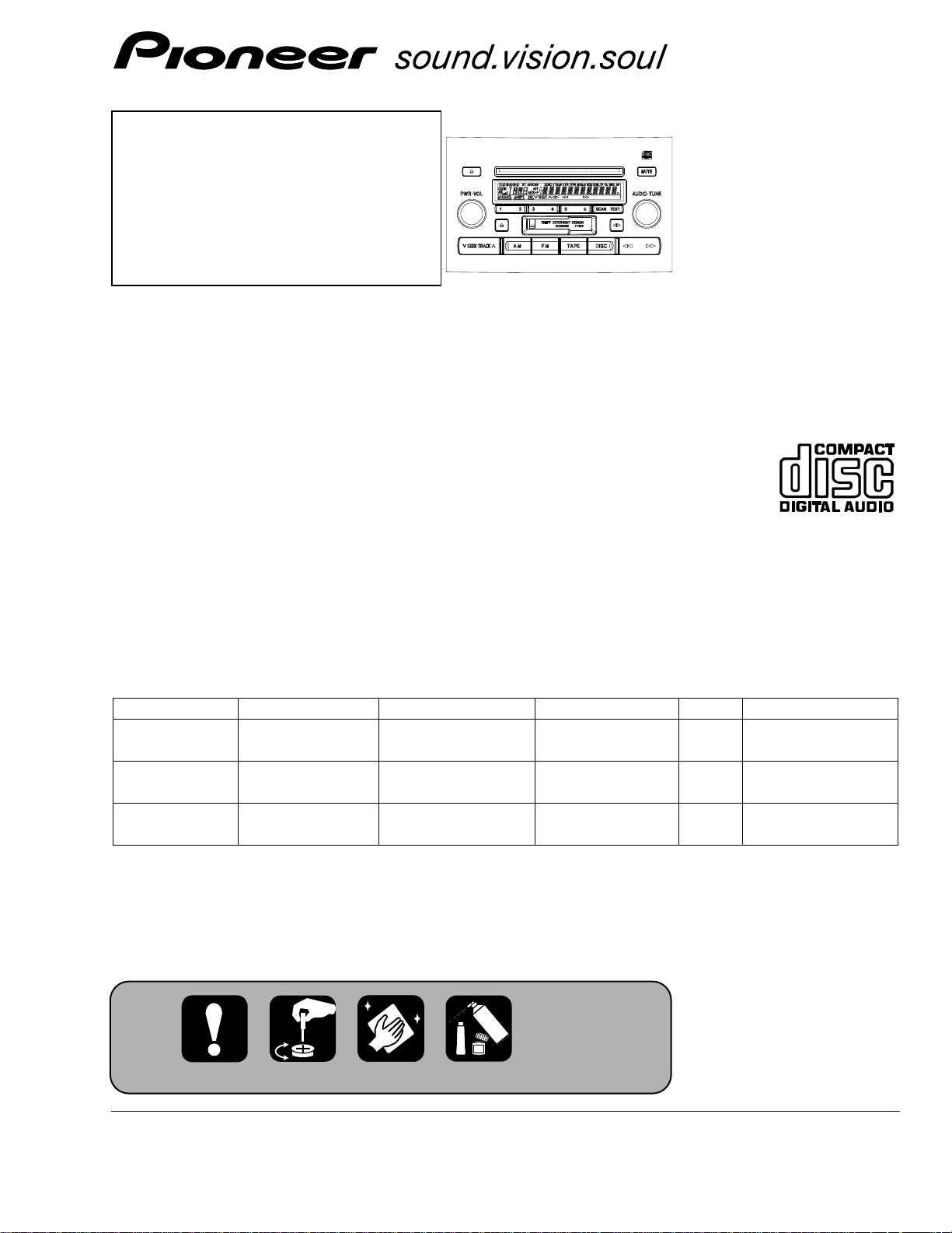
FH-M8527ZT/ES
FH-M8527ZT ES
FH-M8527
ZT-91 ES
FH-M8627ZT ES
FH-M8627ZT-91
ES
FH-M8527ZT CS
FH-M8527ZT-91 CS
VEHICLE DESTINATION PRODUCED AFTER TOYOTA PART No. ID No. PIONEER MODEL No.
LAND CRUISER Middle Near East, August 2002 86120-60530 P7809 FH-M8527ZT/ES
General Area(L) FH-M8527ZT-91/ES
LAND CRUISER Australia, August 2002 86120-60520 P7810 FH-M8627ZT/ES
General Area(R) FH-M8627ZT-91/ES
LAND CRUISER Central/South America August 2002 86120-60540 P7815 FH-M8527ZT/CS
FH-M8527ZT-91/CS
For details, refer to "Important symbols for good services".
Page 2
2
1
234
12
34
F
E
D
C
B
A
FH-M8527ZT/ES
[ Important symbols for good services ]
In this manual, the symbols shown-below indicate that adjustments, settings or cleaning should be made securely.
When you find the procedures bearing any of the symbols, be sure to fulfill them:
2. Adjustments
To keep the original performances of the product, optimum adjustments or specification confirmation is indispensable.
In accordance with the procedures or instructions described in this manual, adjustments should be performed.
3. Cleaning
For optical pickups, tape-deck heads, lenses and mirrors used in projection monitors, and other parts requiring cleaning,
proper cleaning should be performed to restore their performances.
5. Lubricants, glues, and replacement parts
Appropriately applying grease or glue can maintain the product performances. But improper lubrication or applying
glue may lead to failures or troubles in the product. By following the instructions in this manual, be sure to apply the
prescribed grease or glue to proper portions by the appropriate amount.For replacement parts or tools, the prescribed
ones should be used.
4. Shipping mode and shipping screws
To protect the product from damages or failures that may be caused during transit, the shipping mode should be set or
the shipping screws should be installed before shipping out in accordance with this manual, if necessary.
1. Product safety
You should conform to the regulations governing the product (safety, radio and noise, and other regulations), and
should keep the safety during servicing by following the safety instructions described in this manual.
Model No. Order No. Mech. Module Remarks
CX-977 CRT2624 S9 CD Mech. Module:Circuit Description, Mech.Description, Disassembly
CX-1011 CRT2406 3L Cassette Mech. Module:Mech.Description, Disassembly
- This service manual should be used together with the following manual(s):
- Dolby noise reduction manufactured under license from Dolby Laboratories Licensing Corporation.
"Dolby" and the double-D symbol are trademarks of Dolby Laboratories Licensing Corporation.
-
CD section precaution
1. Before disassembling the unit, be sure to turn off the
power. Unplugging and plugging the connectors dur-
ing power-on mode may damage the ICs inside the
unit.
2. To protect the pickup unit from electrostatic dis-
charge during servicing, take an appropriate treat-
ment (shorting-solder, shorting pin, shorting switch)
by referring to “the DISASSEMBLY” on page 68.
3. After replacing the pickup unit, be sure to check the
grating. (See p.58.)
SAFETY INFORMATION
This service manual is intended for qualified service technicians; it is not meant for the casual do-it-yourselfer.
Qualified technicians have the necessary test equipment and tools, and have been trained to properly and safely repair
complex products such as those covered by this manual.
Improperly performed repairs can adversely affect the safety and reliability of the product and may void the warranty.
If you are not qualified to perform the repair of this product properly and safely, you should not risk trying to do so
and refer the repair to a qualified service technician.
Page 3
3
5
6
7
8
F
E
D
C
B
A
5
6
7
8
FH-M8527ZT/ES
CONTENTS
SAFETY INFORMATION ............................................2
1. SPECIFICATIONS........................................................4
2. EXPLODED VIEWS AND PARTS LIST.......................6
3. BLOCK DIAGRAM AND SCHEMATIC DIAGRAM ...14
4. PCB CONNECTION DIAGRAM ................................30
5. ELECTRICAL PARTS LIST ........................................40
6. ADJUSTMENT..........................................................52
7. GENERAL INFORMATION .......................................68
7.1 DIAGNOSIS ........................................................68
7.1.1 DISASSEMBLY .........................................68
7.1.2 CONNECTOR FUNCTION DESCRIPTION .......72
7.2 PARTS .................................................................73
7.2.1 IC................................................................73
7.2.2 DISPLAY....................................................78
7.3 EXPLANATION ...................................................79
7.3.1 SYSTEM BLOCK DIAGRAM.....................79
7.3.2 OPERATIONAL FLOW CHART .................80
7.4 CLEANING ..........................................................81
8. OPERATIONS............................................................82
- The supplementary models are identical with the original ones except for the following items.
Description Part No.
Polyethylene Bag CEG1026
Cover(x2) CEG1045
Carton CHG4861
Contain Box(x1/2) CHL4918(FH-M8527ZT-91/ES)
Contain Box(x1/2) CHL4919(FH-M8627ZT-91/ES)
Contain Box(x1/2) CHL4920(FH-M8527ZT-91/CS)
Air Cap CHW1945(Non Spare Part)
Air Cap(x2) CHW1948(Non Spare Part)
Page 4

4
1
234
12
34
F
E
D
C
B
A
FH-M8527ZT/ES
1. SPECIFICATIONS
General
Power source. . . . . . . . 13.2V(10.5V–16.0V allowable) DC
Grounding system. . . . . . . . . . . . . . . . . . . . Negative type
Backup current . . . . . . . . . . . . . . . . . . . . . . . 0.3mA or less
Dimensions. . . . . . . . . . . . . . 228(W) x134(H) x194(D)mm
Weight. . . . . . . . . . . . . . . . . . . . . . . . . . . . . . . . . . . 2.360kg
Cassette player
Tape. . . . . . . . . . . . . . . . Compact cassette tape(C30-C90)
Tape speed . . . . 4.76cm/sec.(+0.14cm/sec., -0.05cm/sec.)
Wow and flutter . . . . . . . . . . . . . . . . 0.2% or less(WRMS)
Crosstalk . . . . . . . . . . . . . . . . . . . . . . . . . . . . 40dB or more
Stereo Separation . . . . . . . . . . . . . . . . . . . . 30dB or more
S/N . . . . . . . . . . . . . . . . . . . . . . . . . . . . . . . . 40dB or more
Distortion . . . . . . . . . . . . . . . . . . . . . . . . . . . . . . 3% or less
CD player
System . . . . . . . . . . . . . . . . . Compact disc audio system
Usable discs . . . . . . . . . . . . . . . . . . . . . . . . . Compact disc
Signal format . . . . . . . . . . Sampling frequency : 44.1kHz
Number of quantization : 16;linear
S/N . . . . . . . . . . . . . . . . . . . . . . . . . . . . . . . . 65dB or more
Distortion. . . . . . . . . . . . . . . . . . . . . . . . . . . . . 0.3% or less
FM tuner
Frequency range . . . . . . . . . . . . . . . . 87.5–108.0 MHz(ES)
87.9–108.0 MHz(CS)
S/N . . . . . . . . . . . . . . . . . . . . . 46dB or more(54dBµ input)
Distortion. . . . . . . . . . . . . . . . . . . . . . . . . . . . . 1.5% or less
IF interference . . . . . . . . . . . . . . . . . . . . . . . 64dB or more
Image interference. . . . . . . . . . . . . . . . . . . . 35dB or more
Stereo Separation . . . . . . . . . . . . . . . 25dB or more(1kHz)
AM tuner
Frequency range . . . . . . . . . . . . . . . . . 531–1,602 kHz(ES)
530–1,620 kHz(CS)
S/N 20dB usable sensibility . . . . . . . . . . . 34dBµV or less
S/N . . . . . . . . . . . . . . 45dB or more(FH-M8527ZT/ES, CS)
42dB or more(FH-M8627ZT/ES)
Distortion. . . . . . . . . . . . . . . . . . . . . . . . . . . . . 1.5% or less
IF interference . . . . . . . . . . . . . . . . . . . . . . . 40dB or more
Image interference . 40dB or more(FH-M8527ZT/ES, CS)
45dB or more(FH-M8627ZT/ES)
SW1 tuner(FH-M8527ZT/ES)
Frequency range . . . . . . . . . . . . . . . . . . . 2,940–3,575 kHz
3,580–4,215 kHz
4,540–5,175 kHz
5,820–6,455 kHz
7,100–7,735 kHz
S/N 20dB usable sensibility . . . . . . . . . . . 36dBµV or less
S/N . . . . . . . . . . . . . . . . . . . . . . . . . . . . . . . . 42dB or more
Distortion. . . . . . . . . . . . . . . . . . . . . . . . . . . . . 1.5% or less
IF interference . . . . . . . . . . . . . . . . . . . . . . . 40dB or more
Image interference. . . . . . . . . . . . . . . . . . . . 27dB or more
SW2 tuner(FH-M8527ZT/ES)
Frequency range . . . . . . . . . . . . . . . . . . 9,500–10,135 kHz
11,580–12,215 kHz
15,100–15,735 kHz
17,500–18,135 kHz
21,340–21,975 kHz
S/N 20dB usable sensibility . . . . . . . . . . . 36dBµV or less
S/N . . . . . . . . . . . . . . . . . . . . . . . . . . . . . . . . 42dB or more
Distortion. . . . . . . . . . . . . . . . . . . . . . . . . . . . . 1.5% or less
IF interference . . . . . . . . . . . . . . . . . . . . . . . 25dB or more
Image interference. . . . . . . . . . . . . . . . . . . . 25dB or more
Page 5

5
5
6
7
8
F
E
D
C
B
A
5
6
7
8
FH-M8527ZT/ES
Page 6

6
1
234
12
34
F
E
D
C
B
A
FH-M8527ZT/ES
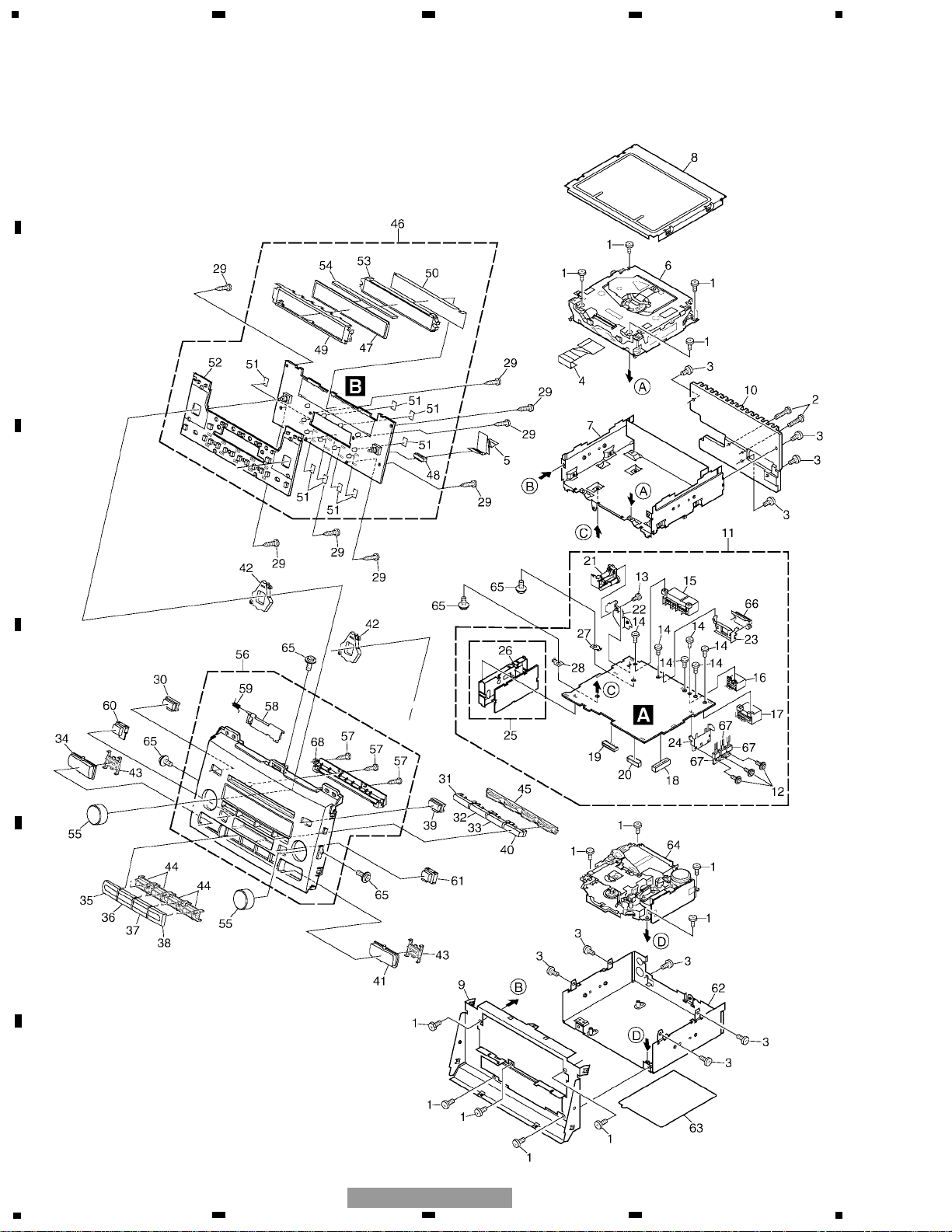
2. EXPLODED VIEWS AND PARTS LIST
2.1 EXTERIOR(FH-M8527ZT/ES, CS)
Page 7
7
5
6
7
8
F
E
D
C
B
A
5
6
7
8
FH-M8527ZT/ES
1 Screw BSZ26P060FMC
2 Screw BSZ26P140FMC
3 Screw BSZ30P080FMC
4 Connector CDE7248
5 Connector CDE6732
6
CD Mechanism Module(S9T) CXK5521
7 Chassis CNA2466
8 Case CNB2721
9 Frame CNC9638
10 Heat Sink CNR1644
11 Main Unit
See Contrast table(2)
12 Screw ASZ26P080FMC
13 Screw BMZ30P040FMC
14 Screw BPZ30P060FSN
15 Connector(CN471) CKM1222
16 Connector(CN473) CKM1350
17 Connector(CN472) CKM1351
18 Connector(CN631) CKS3568
19 Connector(CN601) CKS3835
20 Connector(CN681) CKS4361
21 Connector(CN501) CKX1064
22 Holder CNC9591
23 Holder CNC9592
24 Holder CND1080
25 FM/AM Tuner Unit
See Contrast table(2)
26 Holder CNC8855
27 Terminal(CN474) VNF1084
28 Terminal(CN475) VNF1084
29 Screw BPZ20P080FMC
30 Button(CD EJECT) CAC7203
31 Button(1-2) CAC7205
32 Button(3-4) CAC7206
33 Button(5-6) CAC7207
34 Button(SEEK, TRACK) CAC7211
35 Button(AM) CAC7213
36 Button(FM) CAC7214
37 Button(TAPE) CAC7215
38 Button(DISC) CAC7216
39 Button(MUTE) CAC7328
40 Button(SCAN, TEXT) CAC7329
41 Button(FF, REW) CAC7331
42 Lighting Conductor CNV6895
43 Holder CNV6898
44 Holder CNV6899
45 Holder CNV6956
46 Keyboard Unit CWS1346
47 LCD(LCD901) CAW1700
48 Connector(CN901) CKS4361
49 Holder CNC9700
50 Sheet CNM7733
51 Seal CNM7771
52 Rubber CNV6892
53 Lighting Conductor CNV6894
54 Connector CNV7498
55 Knob Unit CXB8028
56 Grille Unit
See Contrast table(2)
57 Screw BPZ20P060FZK
58 Door
See Contrast table(2)
59 Spring CBH2663
60 Button Assy(TAPE EJECT)CXB8832
61 Button Assy(DIRECTION) CXB8837
62 Chassis Unit CXB8161
63 Shield Unit CXB9781
64
Cassette Mechanism ModuleEXK4295
65 Screw ISS26P060FMC
66 IC(IC801) TDA7386
67
Transistor(Q404, 407, 431) 2SB1185
* 68 Holder Unit CXB8768
Mark No. Description Part No. Mark No. Description Part No.
(1) EXTERIOR(FH-M8527ZT/ES, CS) SECTION PARTS LIST
NOTE:
- Parts marked by “*” are generally unavailable because they are not in our Master Spare Parts List.
- Screws adjacent to ∇ mark on the product are used for disassembly.
- For the applying amount of lubricants or glue, follow the instructions in this manual.
( In the case of no amount instructions, apply as you think it appropriate.)
(2) CONTRAST TABLE
FH-M8527ZT/ES and FH-M8527ZT/CS are constructed the same except for the following:
Part No.
Mark No. Description FH-M8527ZT/ES FH-M8527ZT/CS
11 Main Unit CWM8067 CWM8094
25 FM/AM Tuner Unit CWE1632 CWE1631
56 Grille Unit CXB8164 CXB8340
58 Door CAT2312 CAT2337
Page 8
8
1
234
12
34
F
E
D
C
B
A
FH-M8527ZT/ES
2.2 EXTERIOR(FH-M8627ZT/ES)
Page 9

9
5
6
7
8
F
E
D
C
B
A
5
6
7
8
FH-M8527ZT/ES
1 Screw BSZ26P060FMC
2 Screw BSZ26P140FMC
3 Screw BSZ30P080FMC
4 Connector CDE7248
5 Connector CDE6732
6
CD Mechanism Module(S9T) CXK5521
7 Chassis CNA2466
8 Case CNB2721
9 Frame CNC9638
10 Heat Sink CNR1644
11 Main Unit CWM8068
12 Screw ASZ26P080FMC
13 Screw BMZ30P040FMC
14 Screw BPZ30P060FSN
15 Connector(CN471) CKM1222
16 Connector(CN473) CKM1350
17 Connector(CN472) CKM1351
18 Connector(CN631) CKS3568
19 Connector(CN601) CKS3835
20 Connector(CN681) CKS4361
21 Connector(CN501) CKX1064
22 Holder CNC9591
23 Holder CNC9592
24 Holder CND1080
25 FM/AM Tuner Unit CWE1631
26 Holder CNC8855
27 Terminal(CN474) VNF1084
28 Terminal(CN475) VNF1084
29 Screw BPZ20P080FMC
30 Button(MUTE) CAC7332
31 Button(1-2) CAC7205
32 Button(3-4) CAC7206
33 Button(5-6) CAC7207
34 Button(FF, REW) CAC7334
35 Button(DISC) CAC7289
36 Button(TAPE) CAC7290
37 Button(FM) CAC7291
38 Button(AM) CAC7292
39 Button(CD EJECT) CAC7218
40 Button(SCAN, TEXT) CAC7329
41 Button(SEEK, TRACK) CAC7288
42 Lighting Conductor CNV6895
43 Holder CNV6898
44 Holder CNV6899
45 Holder CNV6956
46 Keyboard Unit CWS1347
47 LCD(LCD901) CAW1700
48 Connector(CN901) CKS4361
49 Holder CNC9700
50 Sheet CNM7733
51 Seal CNM7771
52 Rubber CNV6892
53 Lighting Conductor CNV6894
54 Connector CNV7498
55 Knob Unit CXB8028
56 Grille Unit CXB8165
57 Screw BPZ20P060FZK
58 Door CAT2313
59 Spring CBH2663
60 Button Assy(DIRECTION) CXB8838
61 Button Assy(TAPE EJECT)CXB8835
62 Chassis Unit CXB8161
63 Shield Unit CXB9781
64
Cassette Mechanism ModuleEXK4295
65 Screw ISS26P060FMC
66 IC(IC801) TDA7386
67
Transistor(Q404, 407, 431) 2SB1185
* 68 Holder Unit CXB8768
Mark No. Description Part No. Mark No. Description Part No.
- EXTERIOR(FH-M8627ZT/ES) SECTION PARTS LIST
Page 10
10
1
234
12
34
F
E
D
C
B
A
FH-M8527ZT/ES
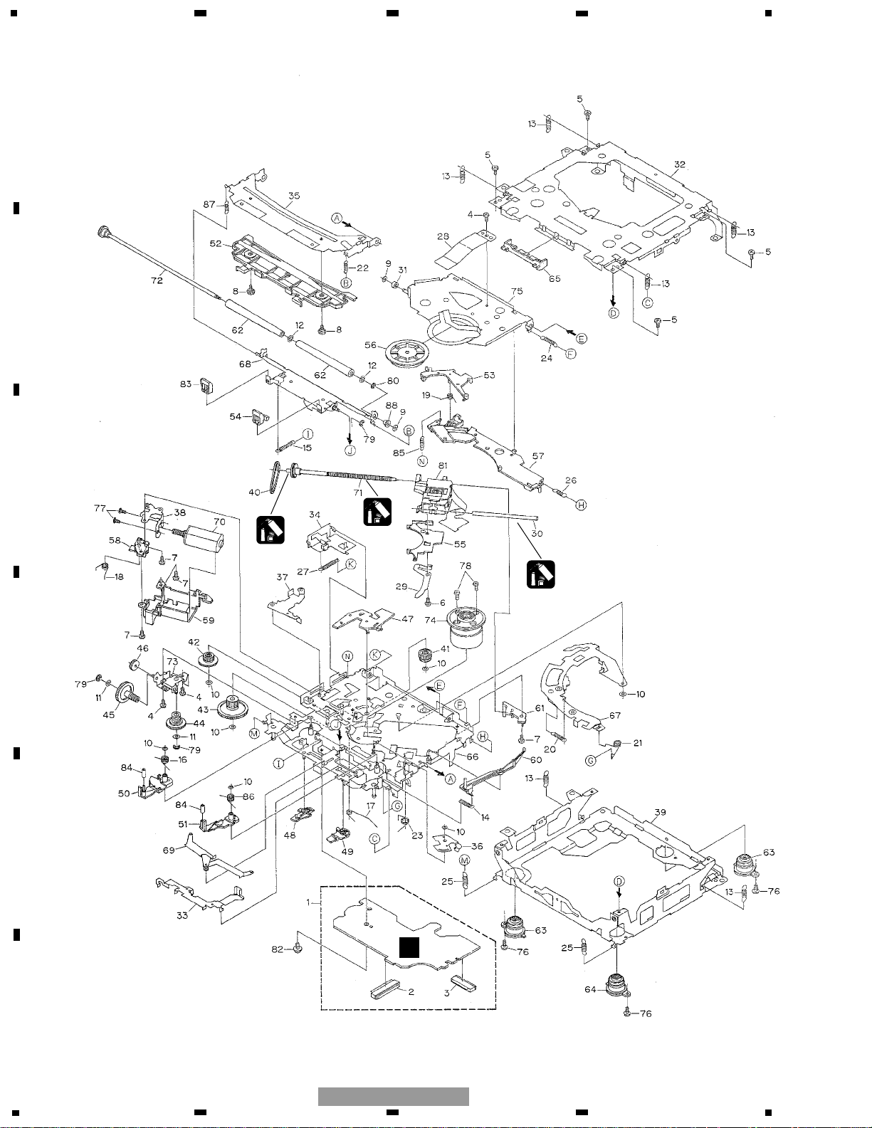
2.3 CD MECHANISM MODULE
UD321BR
GEM1035
GEM1035
C
Page 11

11
5
6
7
8
F
E
D
C
B
A
5
6
7
8
FH-M8527ZT/ES
Mark No. Description Part No. Mark No. Description Part No.
1 Control Unit CWX2608
2 Connector(CN701) CKS1959
3 Connector(CN101) CKS3486
4 Screw BMZ20P025FMC
5 Screw BSZ20P040FMC
6 Screw(M2x4) CBA1362
7 Screw(M2x3) CBA1527
8 Screw CBA1545
9 Washer CBF1037
10 Washer CBF1038
11 Washer CBF1039
12 Washer CBF1060
13 Spring CBH2378
14 Spring CBH2379
15 Spring CBH2514
16 Spring CBH2533
17 Spring CBH2382
18 Spring CBH2383
19 Spring CBH2384
20 Spring CBH2527
21 Spring CBH2386
22 Spring CBH2537
23 Spring CBH2390
24 Spring CBH2391
25 Spring CBH2523
26 Spring CBH2426
27 Spring CBH2444
28 Spring CBL1561
29 Spring CBL1553
30 Shaft CLA3845
31 Roller CLA3910
32 Frame CNC9654
33 Lever CNC9664
34 Lever CNC8949
35 Arm CNC9661
36 Arm CNC9016
37 Arm CNC9017
38 Bracket CNC9123
39 Frame CNC8947
40 Belt CNT1086
41 Gear CNV6886
42 Gear CNV6316
43 Gear CNV6317
44 Gear CNV6318
45 Gear CNV6319
46 Gear CNV6320
47 Arm CNV6322
48 Arm CNV6323
49 Arm CNV6324
50 Arm CNV6888
51 Arm CNV6889
52 Guide CNV6327
53 Arm CNV6924
54 Guide CNV6921
55 Rack CNV6923
56 Clamper CNV6331
57 Arm CNV6332
58 Guide CNV6333
59 Cover CNV6334
60 Arm CNV6335
61 Guide CNV6336
62 Roller CNV6338
63 Damper CNV6175
64 Damper CNV6662
65 Guide CNV6925
66 Chassis Unit CXB7980
* 67 Arm Unit CXB7983
68 Arm Unit CXB7984
69 Arm Unit CXB7985
70 Motor Unit(M2) CXB8284
71 Screw Unit CXB5904
72 Gear Unit CXB8076
73 Bracket Unit CXB7982
74 Motor Unit(M1) CXB6007
75 Arm Unit CXB8504
76 Screw(M2x5) EBA1028
77 Screw JFZ20P020FMC
78 Screw JGZ17P020FZK
79 Washer YE15FUC
80 Washer YE20FUC
81 Pickup Unit(Service)(P9) CXX1482
82 Screw IMS26P030FMC
83 Guide CNV6922
84 Roller CNV6887
85 Spring CBH2509
86 Spring CBH2512
87 Spring CBH2536
88 Collar CNV6906
- CD MECHANISM MODULE SECTION PARTS LIST
Page 12
12
1
234
12
34
F
E
D
C
B
A
FH-M8527ZT/ES
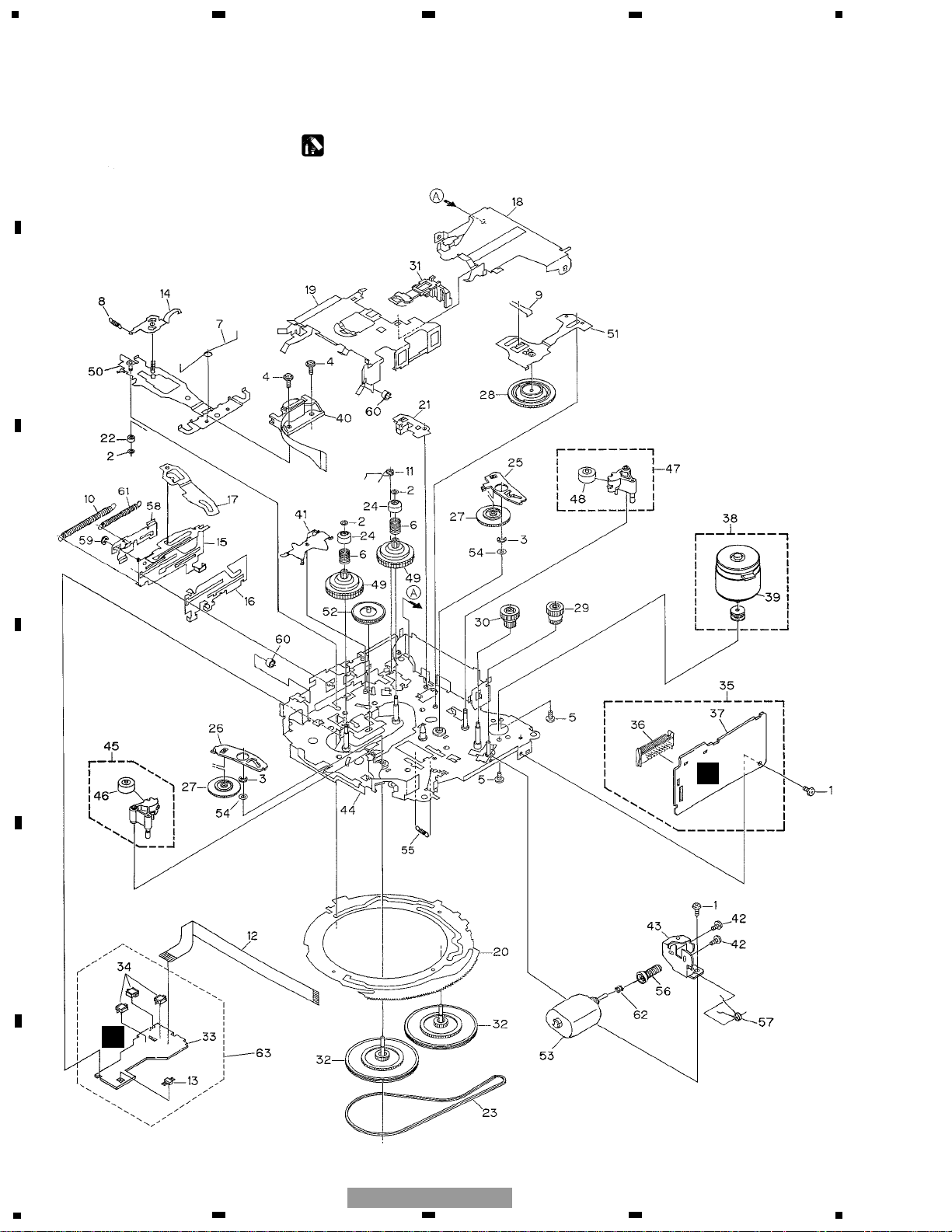
2.4 CASSETTE MECHANISM MODULE
D
E
For grease application, refer to the service manual for CX-1011 (CRT2406).
Page 13

13
5
6
7
8
F
E
D
C
B
A
5
6
7
8
FH-M8527ZT/ES
1 Screw BSZ20P040FMC
2 Washer CBF1037
3 Washer CBG1003
4 Screw EBA1028
5 Screw CBA1037
6 Spring EBH1653
7 Spring EBH1642
8 Spring EBH1641
9 Spring EBH1626
10 Spring EBH1627
11 Spring EBH1648
12 Cord EDD1024
13 Photo-reflector(Q101) EGN1004
14 Arm ENC1526
15 Lever Unit EXA1610
16 Lever ENC1543
17 Arm ENC1532
18 Frame ENC1533
19 Holder ENC1547
20 Gear ENC1535
21 Arm ENC1550
22 Roller ENR1040
23 Belt ENT1027
24 Collar ENV1508
25 Arm ENV1539
26 Arm ENV1540
27 Gear ENV1569
28 Gear ENV1547
29 Gear ENR1044
30 Worm Wheel ENV1559
31 Lever ENV1551
32 Flywheel ENV1554
33 Gathering PCB ENX1073
34 Switch(S101,S102,S103) ESG1007
35 Deck Unit EWM1043
36 Plug(CN251) CKS3540
37 Gathering PCB ENX1076
38 Motor Unit(M1) EXA1618
39 Motor EXM1035
40 Head Assy(HD1) EXA1594
41 Arm ENC1537
42 Screw JGZ20P025FNI
43 Bracket ENC1559
44 Chassis Unit EXA1636
45 Pinch Holder Unit EXA1608
46 Pinch Roller ENV1518
47 Pinch Holder Unit EXA1607
48 Pinch Roller ENV1518
49 Reel Unit EXA1625
50 Head Base Unit EXA1611
51 Lever Unit EXA1587
52 Gear Unit EXA1596
53 Motor Unit(M2) EXA1623
54 Washer HBF-179
55 Spring EBH1537
56 Worm Gear ENV1564
57 Spring EBH1655
58 Lever ENC1548
59 Washer YE15FUC
60 Tube ENM1039
61 Spring EBH1645
62 Spring EBH1545
63 Sensor Unit EWM1041
Mark No. Description Part No. Mark No. Description Part No.
- CASSETTE MECHANISM MODULE SECTION PARTS LIST
Page 14
14
RFGND
IC 3
EEPROM
FM/AM 1ST IF 10.7MHz
T51 Q51 CF51
CF52 CF53
IC1
MIXER, IF AMP, DET.
6
21
COMP
25
CF202
VDD
VCC
DI/DO
CE2CKCE1SLFMSD
IC 2 FM MPX
AMANT
FMANT
ATT
ATT
AMRF
FMRF
IMG ADJ
RF ADJ
X901
10.25MHz
ANT ADJ
LOCL
AMDET
MPXREF 41kHz
AM 2ND IF
450kHz
DGND
STIND
L ch
AMDET
AMPNS
27
26
28
FM/AM TUNER UNIT
22 10 14 12 15 16 13 211 1 9
17
SUB
ANT
MAIN
ANT
IC 501
LA1061M
6
5
2
13
FM DIVER
AM PNS
16
3
9
IC 561
HA12181FP
HPF and LPF
VCC
SWVDD
Q501
Q504
Q561
Q502
SWVDD
ACC
BU
CN701
Q101
M
LASER
DIODE
MONITOR
DIODE
CLAMP
SENSE
DISC
SENSE
FOCUS ACT.
SPINDLE
MOTOR
M
LOADING
/CARRIAGE
MOTOR
TRACKING ACT.
LDMD
FO+
TO+
HOLOGRAM
UNIT
IC 401
BA5996FM
IC 201
TC9495FP
IC 701
BA05SFP
5V REGULATOR
SERVO
CONTROL,
DSP,
LPF, DAC
ACT
/MOTOR
DRIVER
DSCSNS
VD
VD
VDD
CONT
LOEJ
L-OUT
CD5VON
CN101
TOP
FOP
16
SOP
15
SOM
17
LCOP
18
LCOM
22
1
2
LOEJ
78
85
LO
79
9
MUTE
12
FOP
TD/FD
AC,BD
F,E
SD/MD
38
RFI
43
FEI
4
14
TOP
S901
HOME
12EJ
SENSE
8EJ
SENSE
HOME
LD+
VDD
9
LDO
8
MDI
IC 101
TA2153FN
RFRPIN
FEO
TEO
24
16
14 46
TEI
RF-AMP
PICKUP UNIT
CONTROL UNIT
15
5
4
1
14
17
2
11
10
14
16
1
17
2
11
10
14
16
1
AVC-LAN
L+
3
CN473
TAPE+B
CSL
BU
stby
mtl
LOAD
CN631
L–
2
MUTE
1
ACC+B
11
BU+B
12
TX+
9
TX–
10
TX1+
2
CN472
TX1–
1
SW1
4
SW2
3
BU
AUDIO+B
IC 331
NJM4558MD
5
6
7
AVC-LAN DEF AMP
IC 781
HA12187FP
6
5
1
2
8
BUS DRIVER
L
CN601
B.U
MTL
LOAD
IC251
CXA2559Q
IC351
PA2020A
EQ AMP
MECHANISM
DRIVER
CN251
CN252
CN254
CN255
CN253
7
5
TAPE+B
Lch
18
FWD
L-ch
REV
L-ch
37
36
39
18
19
17
8710
CN256
S1
LOAD
S2
MODE
EGN1
REEL
SENSE
M
M
M2
SUB
MOTOR
M1
MAIN
MOTOR
5
2
1
S3
70µs
DECK UNIT
REEL SENSE PCB
5
1
4
2
1
3
4
11
20
19
8
3
4
11
20
19
8
315 6
135 64
LOEJ
CONT
DISCSENS
HOME
CDVD9V
CD5VON
12
VDD
FMB
RESET IC
IC782
S-80735ANDZI
SWVDD
SWVDD
VDD
Q422
MOTHER UNIT
LAN MUTE
Q701
FMPW
AMPW
AMB
FM/AM SW
Q563
Q565
Q564
A
D
E
C
stby
1
234
12
34
F
E
D
C
B
A
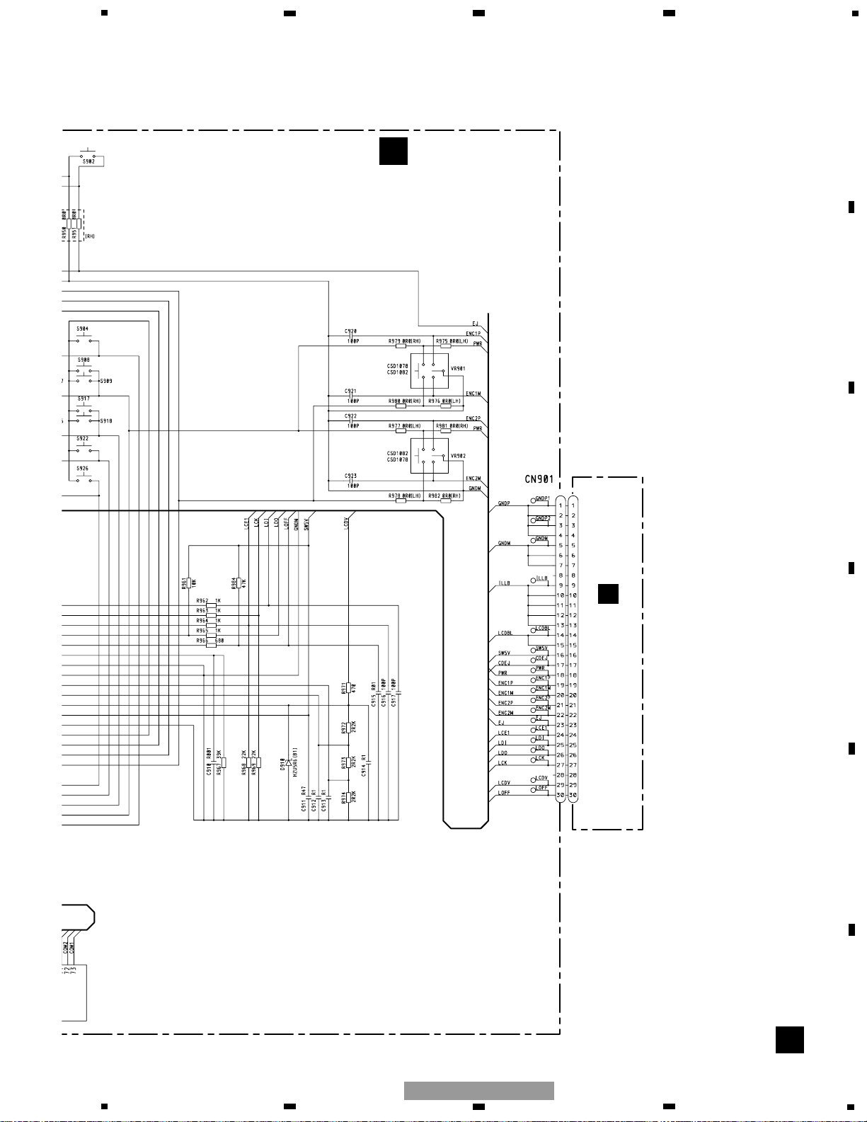
FH-M8527ZT/ES
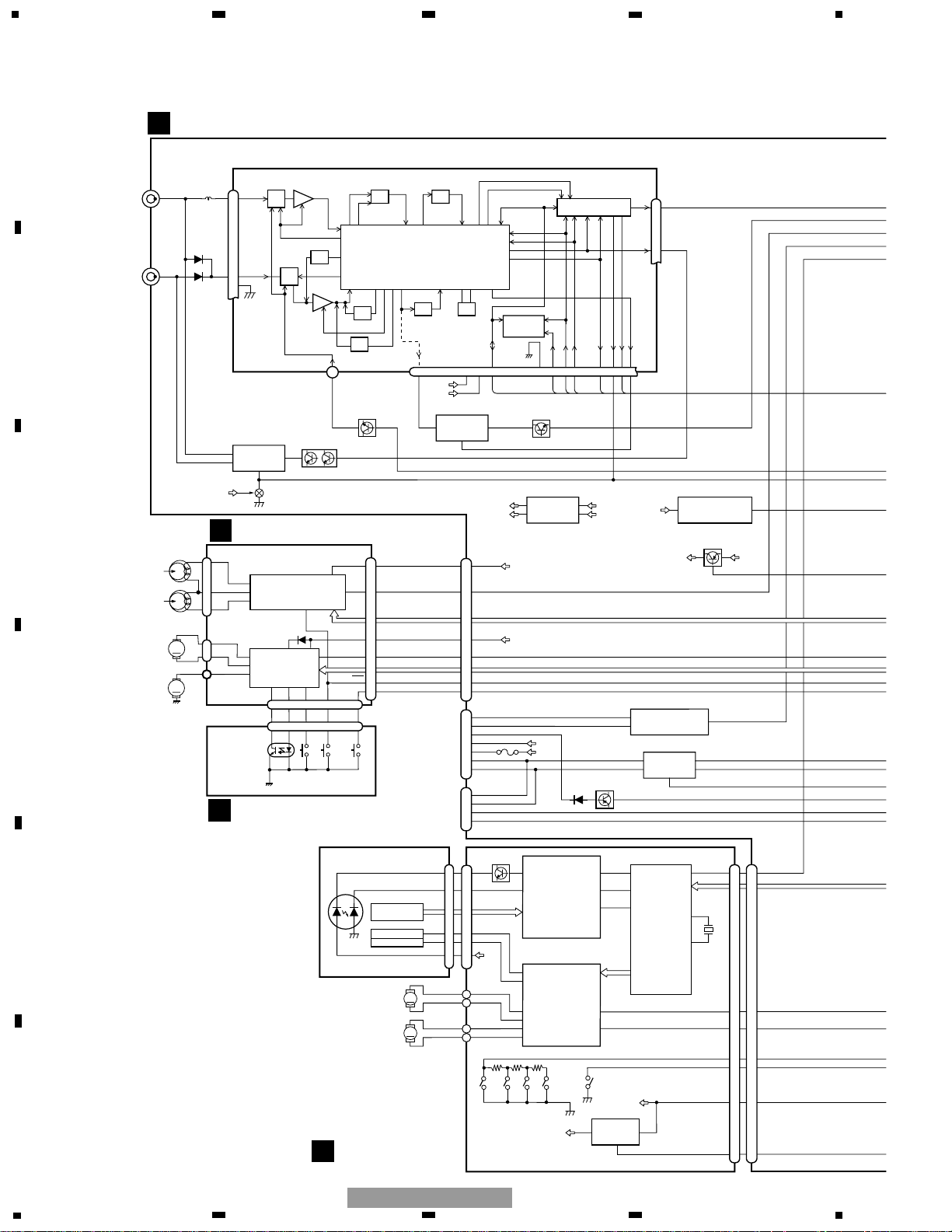
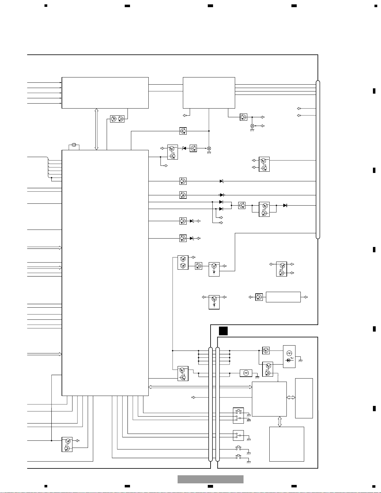
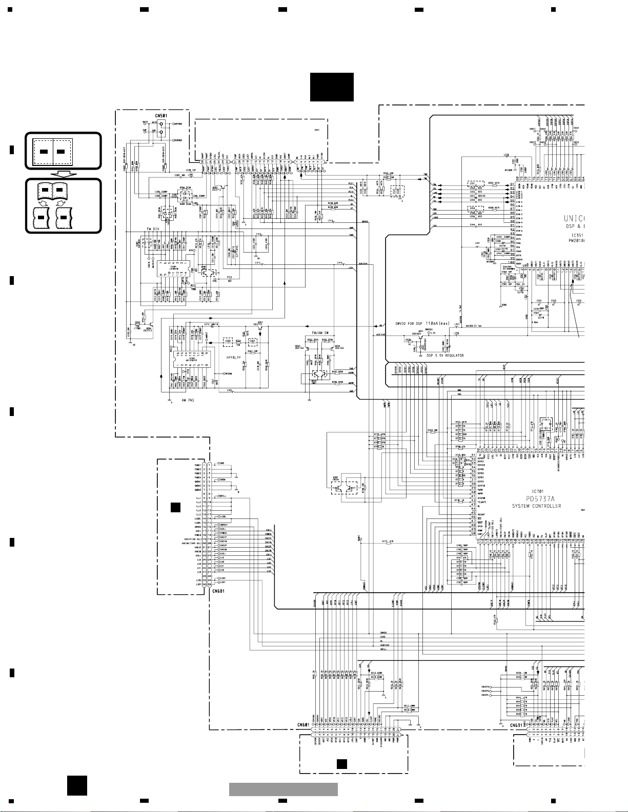
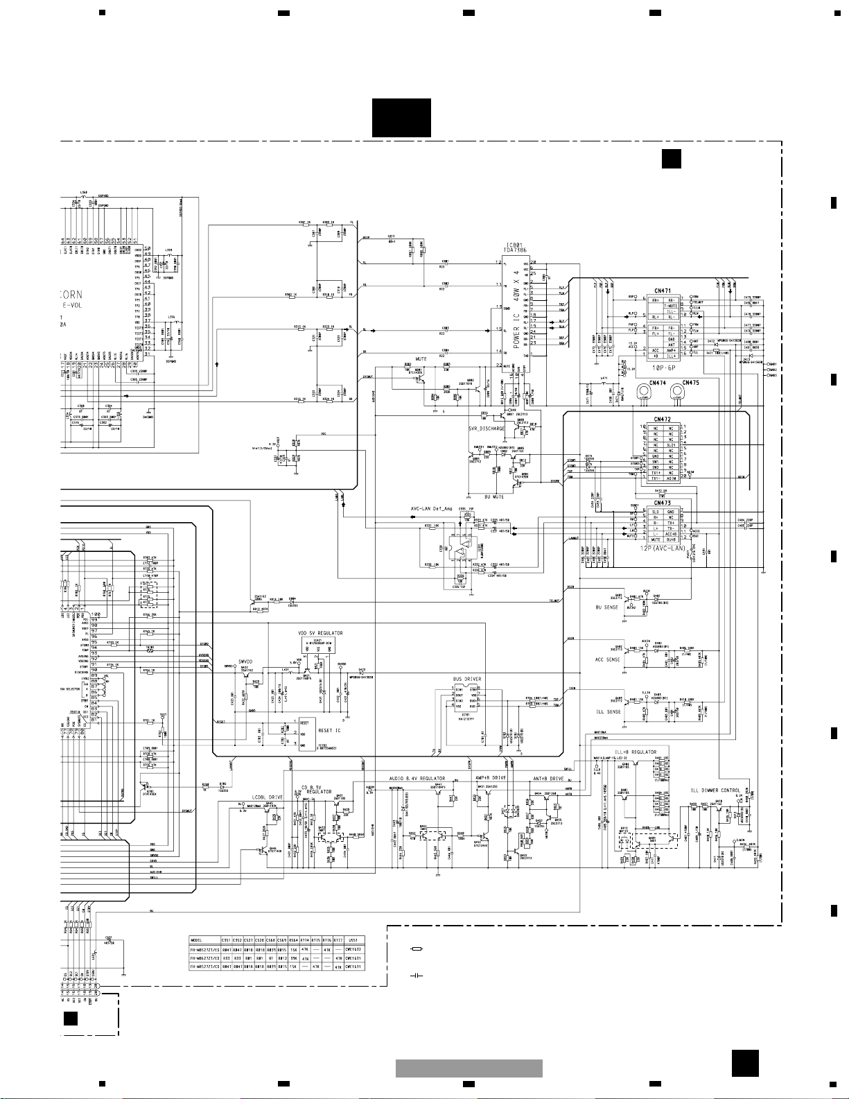
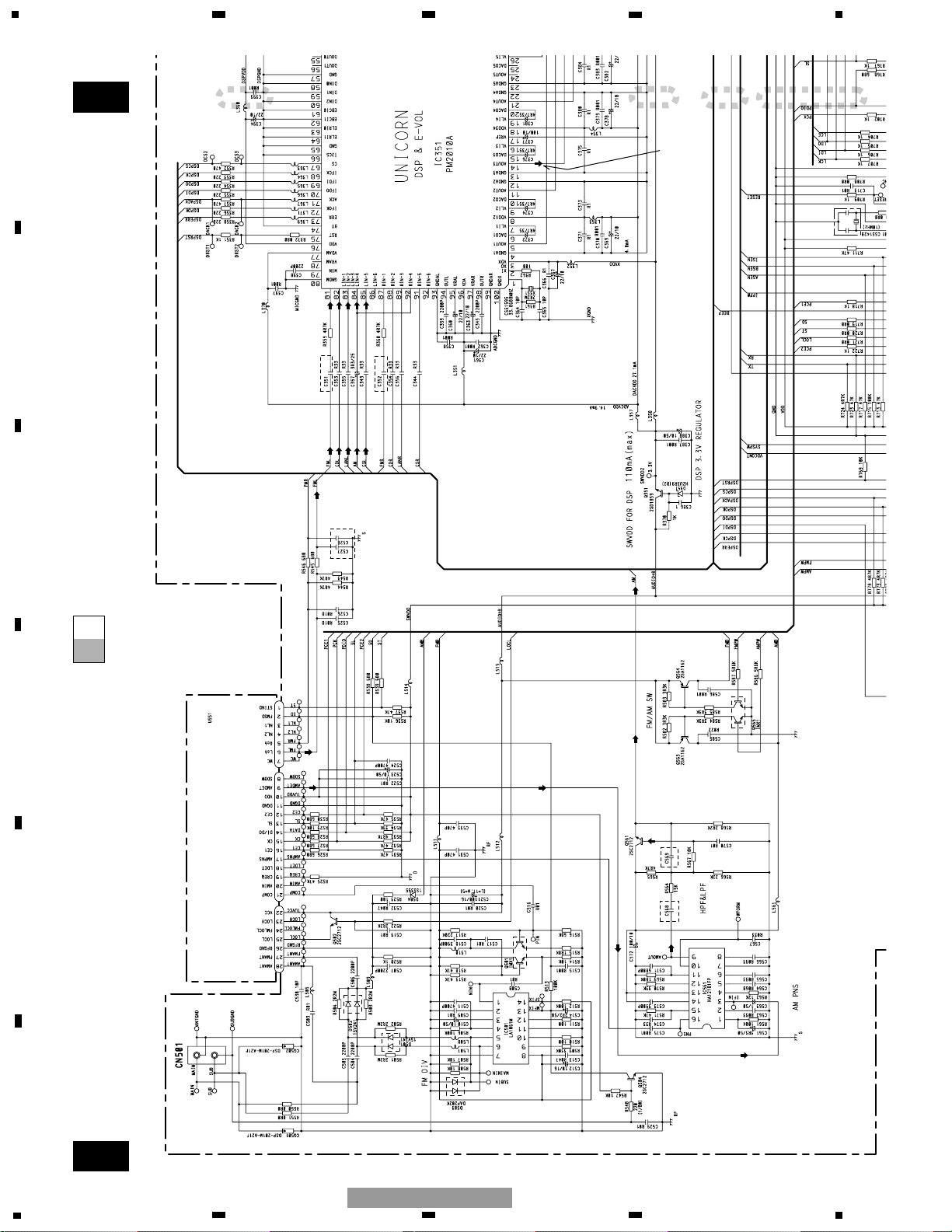
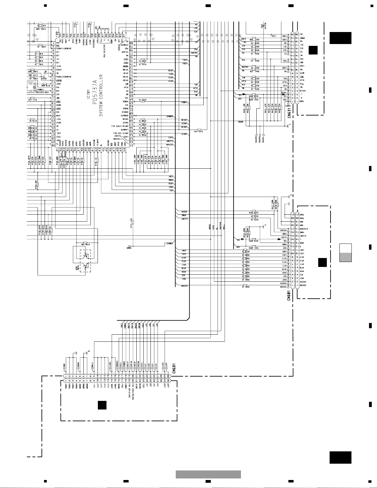
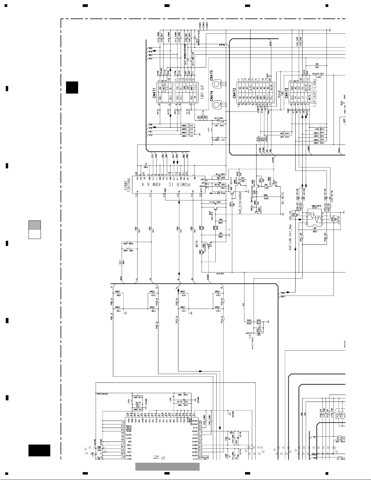
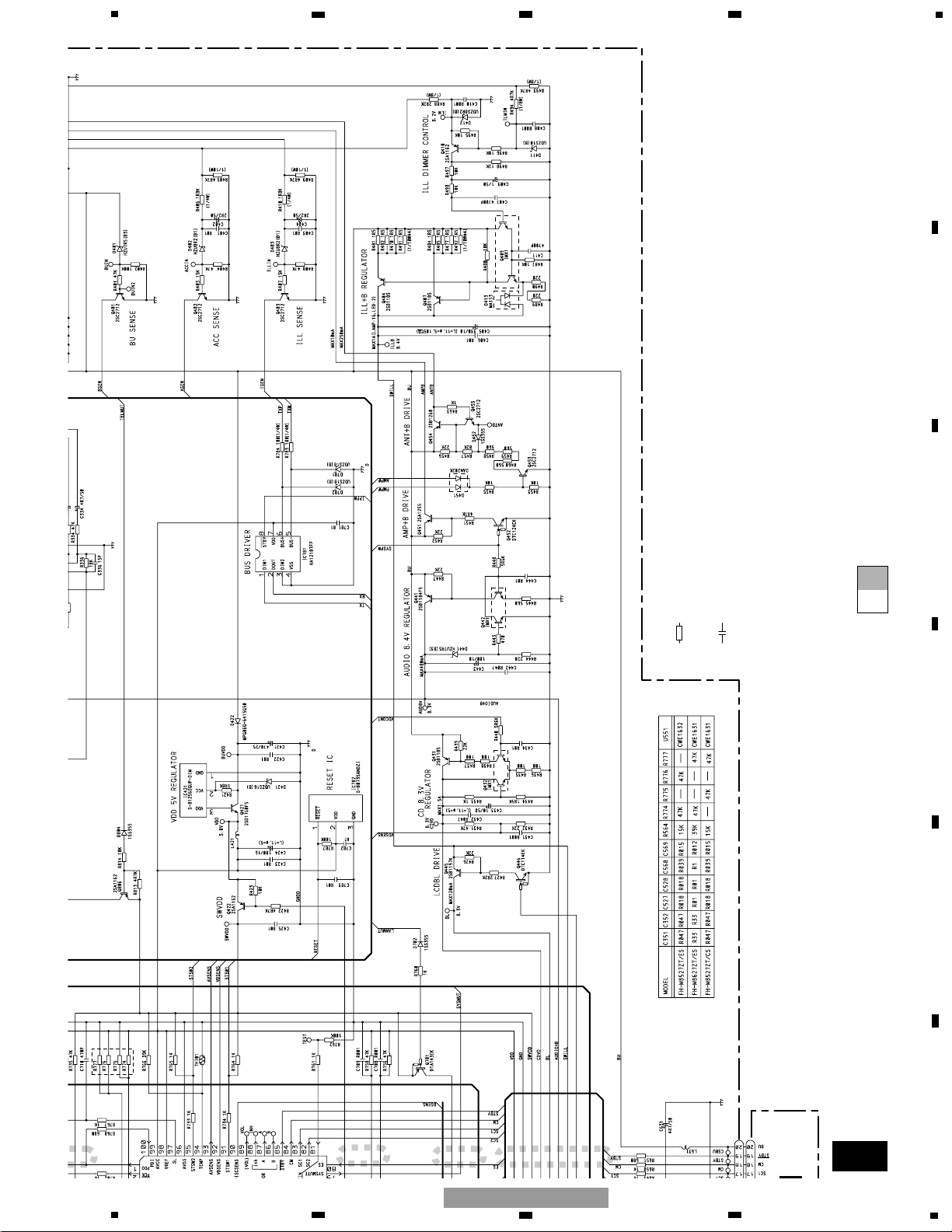
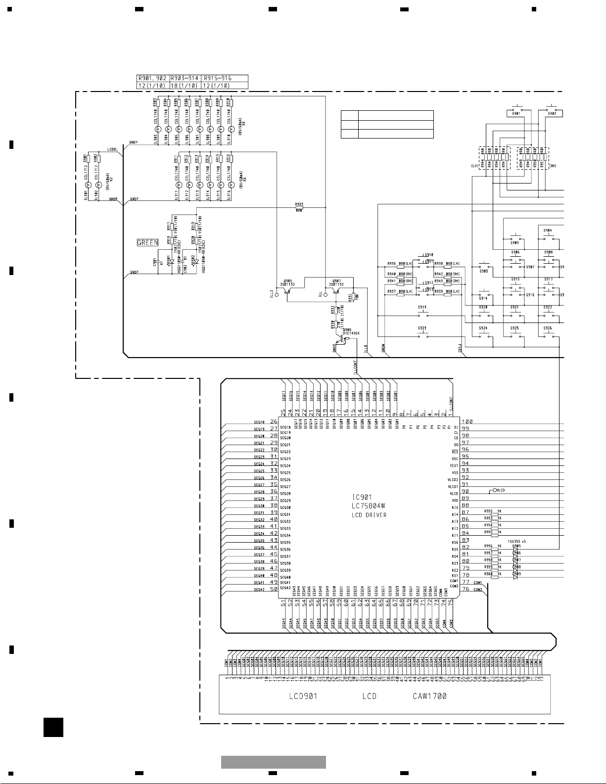
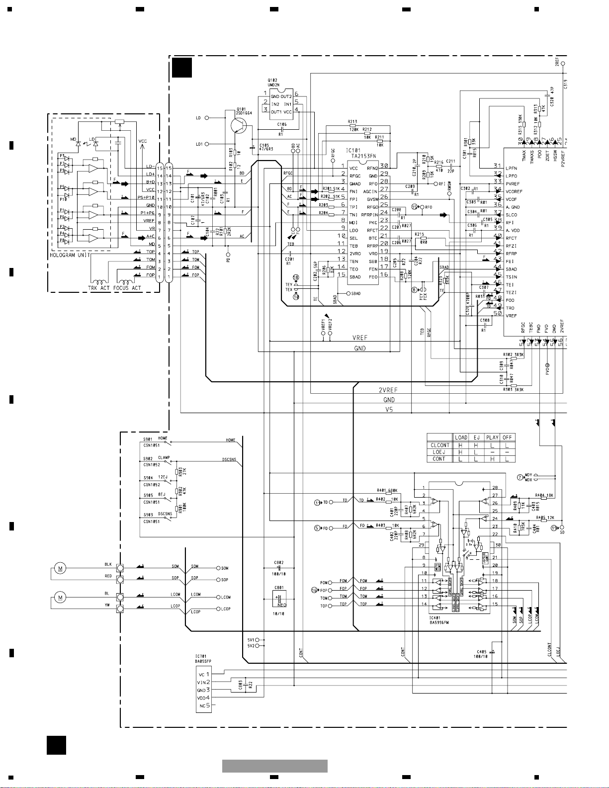
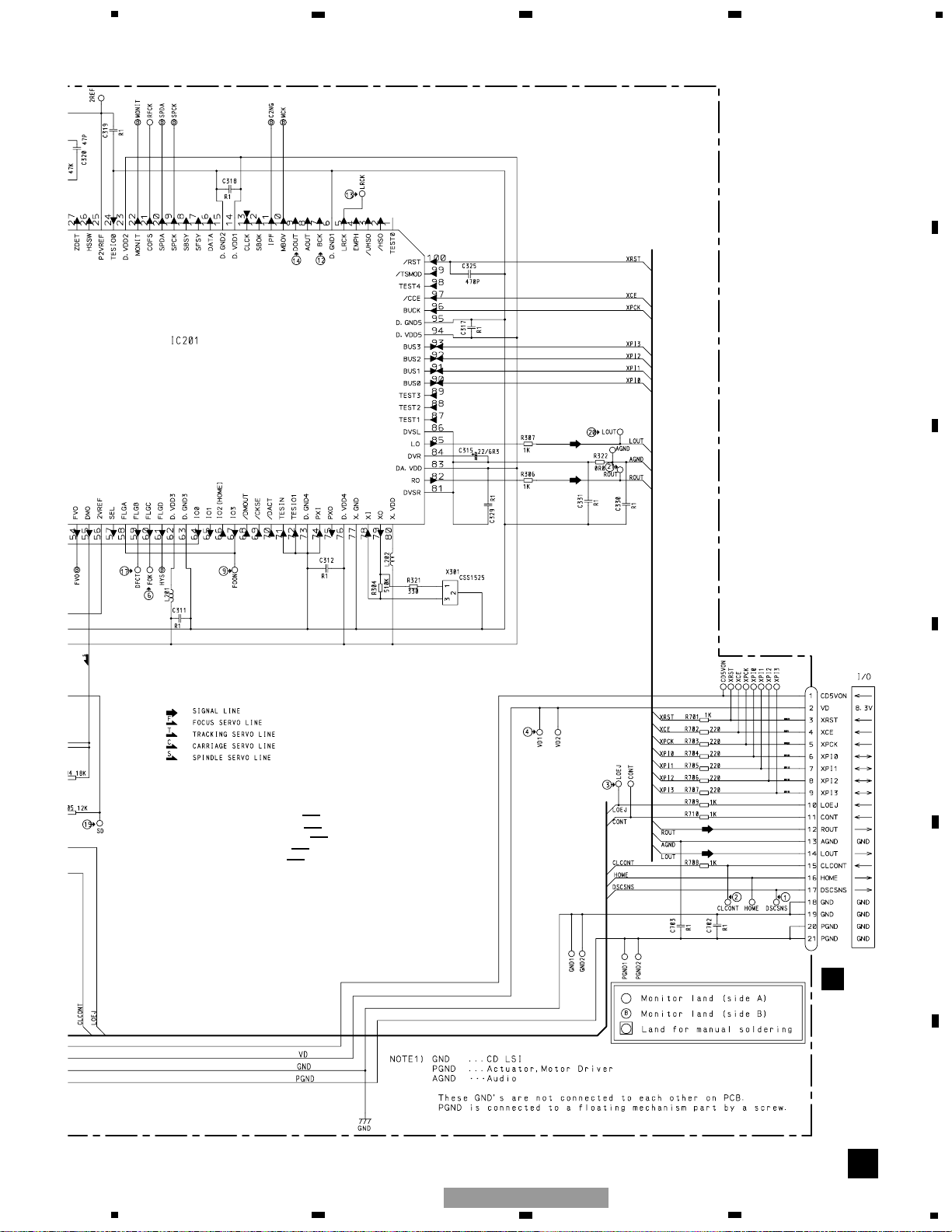
3. BLOCK DIAGRAM AND SCHEMATIC DIAGRAM
3.1 BLOCK DIAGRAM
Page 15
15
SYSTEM CONTROLLER
IC 701
PD5737A
LIN-1
LIN-2
LIN-3
LIN-4
81
512
AOUT1
IC 351
PM2010A
DSP and E. VOL
82
84
LIN-5
FL
14 15
AOUT3
RL
85
IFDO
70
STBY4MUTE
22
SVR
10
83
ST
XOUTXIN
26
SL
97
PCE1
23
pck
2
PCE2
28
PDI
100
PDO
1
LOCL
27
SD
25
stby
85
mtl
68
CSLOAD
77
LANMUTE
55
TX
30
RX1
29
IPPW
22
STSW1
91
STSW2
95
LOEJ53CONT50DISCSENS90HOME
49
CD5VON51VDCONT
45
cdej74csej75ENC2M58ENC2P
57
ENC1M/(TAPE SEL)
56
ENC1P/(CD SEL)
54
POWER
63
Q307
13
DSPDI
36
SYSMUTE
79
15
X701
10MHz
Q801
Q805
Q804
Q803
Q802
VCC
SYSPW
MUTE
ACC SENSE
BU MUTE
WF AMP+B
41
SYSPOW
20
asen
39
FMPW
40
AMPW
Q402
ACC
BU SENSE
19
bsen
Q401
BU
ILL SENSE
18
isen
42
TELMUTE
Q403
TEL MUTE
Q806
FL+
3
CN471
FL–
12
RL+
5
RL–
10
ILL+
16
AMP+
15
T -MUTE
8
ILL–
9
5
FL+
3
FL–
17
RL+
19
RL–
IC 801
TDA7386
POWER IC
SVR_DISCHARGE
Q807
Q808
VCC
SYSPW
KEYBOARD UNIT
9
10
11
12
13
14
15
ILLBILL1
ILL2
ILL3
ILL4
ILL5
LCDBL
LCDBL
SWVDD
POWER
ENC1P/(CD SEL)
ENC1M/(TAPE SEL)
ENC2P
ENC2M
CSEJ
CDEJ
LCDBL
SW 5V
16
PWR
18
19
20
ENC1P
ENC1M
Q905
Q907
Q908
ILL LAMP x 14
ILL LED x 2
CN901
CN681
BL LAMP x 2
LDO/LDI/LCE/LCK
LCDV/LOFF
1
89
VDD
P1
LCD DRIVER
IC901
LC75804W
POWER-VOL
LCD
CAW1700
EJ
23
CDEJ
17
21
22
9
10
11
12
13
14
15
16
18
19
20
23
17
21
22
ENC2P
ENC2M
AUDIO CONTROL
S901
CSEJ
S913
CDEJ
Q453
Q454
Q455
ANT
14
ANT+B
Q451
Q452
BU
SYSPW
SYSPW
KEY
MATRIX
SWVDD
Q445
Q446
43
BL
LCDBL DRIVE
ILL+B
ILL DIMMER
CONTROL
AUDIO+B
BU
AUD8V
SYSPW
DSPVDD
Q441
Q442
AUDIO 8.4V REGULATOR
SWVDD FOR DSP
Q351
BU
VDD
VDD 5V REGULATOR
IC421
S-81256SGUP-DIM
Q421
12
reset
73
swvdd
BU
Q431
Q432
92
CD 8.3V
REGULATOR
VDSENS
+B
1
BU
ACC
2
ACC
ACC
Q410
Q409
BU
Q404
Q407
FMB
AMB
B
5
6
7
8
F
E
D
C
B
A
5
6
7
8
FH-M8527ZT/ES
Page 16
16
B
CN901
C
CN701
FM/AM TUNER UNIT
CD:+4.2dBs
(1kHz 0dB 1180±100mVrms)
TAPE:-7.3dBs
-8.2dBs(ACT-150,200nWb/m)
-7.3dBs(TCC-140,250nWb/m)
AM:-12.7dBs(DET out=-12.7±2dBs)
FM: (400Hz,30%mod -30dBs)
AM:-27.0dBs
FM:-28.0dBs
CD: 0dBs
LAN: 0dBs
TAPE:-11.1dBs
AM: -9.2d
FM:-12.0d
CD: +1d
LAN: +1d
TAPE: -5.1d
1
234
12
34
F
E
D
C
B
A
FH-M8527ZT/ES
3.2 OVERALL CONNECTION DIAGRAM(GUIDE PAGE)
Note: When ordering service parts, be sure to refer to “EXPLODED VIEWS AND PARTS LIST” or “ELECTRICAL PARTS
LIST”.
A-a
A-b
A-b
A-a
A-a
A
Large size
A-b
A-b
SCH diagram
Guide page
Detailed page
A-a A-b
A-a
A-a
Page 17
17
600µH
D
CN251
A
MAIN UNIT
Decimal points for resistor
and capacitor fixed values
are expressed as :
2.2 2R2
0.022 R022
←
←
The > mark found on some component parts indicates
the importance of the safety factor of the part.
Therefore, when replacing, be sure to use parts of
identical designation.
Symbol indicates a resistor.
No differentiation is made between chip resistors and
discrete resistors.
NOTE :
Symbol indicates a capacitor.
No differentiation is made between chip capacitors and
discrete capacitors.
>
2dBs
0dBs
1dBs
AM:+16.8dBs
FM:+14.0dBs
CD: +27dBs
LAN: +27dBs
TAPE:+20.9dBs
LAN:+8.23dBs
(1kHz 0dB
±1Vrms(+8.23dB)
5
6
7
8
F
E
D
C
B
A
5
6
7
8
FH-M8527ZT/ES
A-b
A
Page 18
18
A-a
A-b
A-a
A-a
A-b
1
2
3
4
FM/AM TUNER UNIT
AM:-12.7dBs(DET out=-12.7±2dBs)
FM: (400Hz,30%mod -30dBs)
AM:-27.0dBs
FM:-28.0dBs
CD: 0dBs
LAN: 0dBs
TAPE:-11.1dBs
AM: -9.2dBs
FM:-12.0dBs
CD: +1dBs
LAN: +1dBs
TAPE: -5.1dBs
1
234
12
34
F
E
D
C
B
A
FH-M8527ZT/ES
Page 19
19
A-a
A-b
A-a
A-a
A-b
5
6
7
B
CN901
C
CN701
D
CN251
CD:+4.2dBs
(1kHz 0dB 1180±100mVrms)
TAPE:-7.3dBs
-8.2dBs(ACT-150,200nWb/m)
-7.3dBs(TCC-140,250nWb/m)
5
6
7
8
F
E
D
C
B
A
5
6
7
8
FH-M8527ZT/ES
Page 20
20
A-a
A-b
A-b
1
2
3
4
600µH
A
MAIN UNIT
>
AM:+16.8dBs
FM:+14.0dBs
CD: +27dBs
LAN: +27dBs
TAPE:+20.9dBs
LAN:+8.23dBs
(1kHz 0dB
±1Vrms(+8.23dB)
1
234
12
34
F
E
D
C
B
A
FH-M8527ZT/ES
Page 21
21
A-a
A-b
A-b
5
6
7
CN251
Decimal points for resistor
and capacitor fixed values
are expressed as :
2.2 2R2
0.022 R022
←
←
The > mark found on some component parts indicates
the importance of the safety factor of the part.
Therefore, when replacing, be sure to use parts of
identical designation.
Symbol indicates a resistor.
No differentiation is made between chip resistors and
discrete resistors.
NOTE :
Symbol indicates a capacitor.
No differentiation is made between chip capacitors and
discrete capacitors.
5
6
7
8
F
E
D
C
B
A
5
6
7
8
FH-M8527ZT/ES
Page 22
22
B
1
5
2
6
FF(
SEEK T
UP(
REW(LH)
SEEK TRACK
DOWN(RH)
SEEK TRACK
UP(LH)
FF(RH)
SEEK TRACK
DOWN(LH)
REW(RH)
TEXTSCAN
34
FM(LH)
TAPE(RH)
AM(LH)
DISC(RH)
DISC(LH)
AM(RH)
TAPE(LH)
FM(RH)
CD EJECT(LH)
MUTE(RH)
MUTE(LH)
CD EJECT(RH)
DIRECTION(LH
TAPE EJECT(RH
TAPE EJECT(LH)
DIRECTION(RH)
LH
RH
LH
FH-M8527ZT/ES
FH-M8627ZT/ES
FH-M8527ZT/CS
5.4V
1
234
12
34
F
E
D
C
B
A
FH-M8527ZT/ES
3.3 KEYBOARD UNIT
Page 23
23
B
A
CN681
B
KEYBOARD UNIT
43
2
51
43
2
51
FF(LH)
SEEK TRACK
UP(RH)
PWR•VOL(LH)
AUDIO•TUNE(RH)
AUDIO•TUNE(LH)
PWR•VOL(RH)
TEXT
4
FM(LH)
TAPE(RH)
DISC(LH)
AM(RH)
DIRECTION(LH)
TAPE EJECT(RH)
5
6
7
8
F
E
D
C
B
A
5
6
7
8
FH-M8527ZT/ES
Page 24
24
C
M1 CXB6007
M2 CXB8284
LOADING/CARRIAGE
SPINDLE
RF AMP
S
ACT/MOTOR DRIVER
5V REGULATOR
CN101
91K
91K
PICKUP UNIT
(SERVICE)(P9)
C
CONTROL UNIT
1
234
12
34
F
E
D
C
B
A
FH-M8527ZT/ES
3.4 CD MECHANISM MODULE
Page 25
25
C
16.934MHz
SERVO CONTROL/DSP/DAC/LPF
CN701
TC9495FP
A
CN601
SWITCHES:
CONTROL UNIT
S901 : HOME SWITCH.....ON-OFF
S902 : CLAMP SWITCH....ON-OFF
S903 : DSCSNS SWITCH....ON-OFF
S904 : 12EJ SWITCH....ON-OFF
S905 : 8EJ SWITCH....ON-OFF
The underlined indicates the switch position.
5
6
7
8
F
E
D
C
B
A
5
6
7
8
FH-M8527ZT/ES
Page 26
26
1
234
12
34
F
E
D
C
B
A
FH-M8527ZT/ES
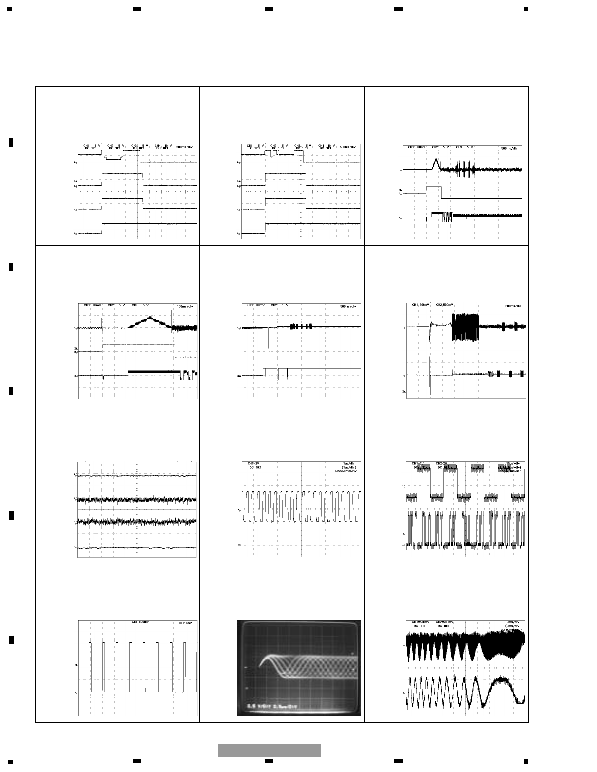
@ CH1:BCK 2V/div.
During "Play"
1 CH1:DSCSNS 5V/div.
2 CH2:CLCONT 5V/div.
3 CH3:LOEJ 5V/div.
4 CH4:VD 10V/div.
When loading (8 cm CD)
500ms/div.
5 CH1:FD 500mV/div.
6 CH2:FOK 5V/div.
7 CH3:MD 5V/div.
When setting up "Source On"
500ms/div.
8 CH1:FE 500mV/div.
9 CH2:FOON 5V/div.
When setting up "Source On"
500ms/div.
5 CH1:FD 500mV/div.
6 CH2:FOK 5V/div.
7 CH3:MD 5V/div.
Magnified drawing for "time"
100ms/div.
1 CH1:DSCSNS 5V/div.
2 CH2:CLCONT 5V/div.
3 CH3:LOEJ 5V/div.
4 CH4:VD 10V/div.
When loading (12 cm CD)
Ref. :
GND
Mode :
Normal
Ref. :
GND
Mode :
Normal
Ref. :
VREF
Mode :
Normal
Ref. :
VREF
Mode :
Normal
Ref. :
VREF
Mode :
Normal
Ref. :
VREF
Mode :
Normal
Ref. :
VREF
Mode :
Normal
Ref. :
VREF
Mode :
Normal
Ref. :
VREF
Mode :
Normal
Ref. :
VREF
Mode :
Test
Ref. :
VREF
Mode :
Normal
Ref. :
VREF
Mode :
Normal
500ms/div.
0 CH1:TE 500mV/div.
8 CH2:FE 500mV/div.
When setting up "Source On"
200ms/div.
1µs/div.
# CH1:LRCK 2V/div.
$ CH2:DOUT 2V/div.
During "Play"
10µs/div.
7 CH1:MD 500mV/div.
During "Play"
10µs/div.
% CH1:RFO 500mV/div.
During "Play"
0.5µs/div.
% CH1:RFO 500mV/div.
0 CH2:TE 500mV/div.
During "Tracking Open"
2ms/div.
8 CH1:FE 500mV/div.
5 CH2:FD 500mV/div.
0 CH3:TE 500mV/div.
! CH4:TD 500mV/div.
During "Play"
1ms/div.
- Waveforms
Note:1. The encircled numbers denote measuring pointes in the circuit diagram.
2. Reference voltage
VREF:2.1V
Page 27

27
5
6
7
8
F
E
D
C
B
A
5
6
7
8
FH-M8527ZT/ES
% CH1:RFO 1V/div.
0 CH2:TE 500mV/div.
& CH3:DFCT 5V/div.
During inside/outside search
200ms/div.
% CH1:RFO 1V/div.
0 CH2:TE 500mV/div.
! CH3:TD 1V/div.
1 Track Jump
500µs/div.
% CH1:RFO 1V/div.
0 CH2:TE 1V/div.
! CH3:TD 1V/div.
100 Track Jump
5ms/div.
% CH1:RFO 1V/div.
0 CH2:TE 1V/div.
! CH3:TD 1V/div.
32 Track Jump
5ms/div.
5 CH1:FD 1V/div.
^ CH2:FOP 2V/div.
With no disk inserted
During "Focus Close"
200ms/div.
1 CH1:DSCSNS 5V/div.
2 CH2:CLCONT 5V/div.
3 CH3:LOEJ 5V/div.
When "Eject" (8cm CD)
200ms/div.
* CH1:TEY 500mV/div.
( CH2:SD 2V/div.
During inside/outside search
200ms/div.
1 CH1:DSCSNS 5V/div.
2 CH2:CLCONT 5V/div.
3 CH3:LOEJ 5V/div.
When "Eject" (12 cm CD)
200ms/div.
% CH1:RFO 2V/div.
& CH2:DFCT 5V/div.
5 CH3:FD 1V/div.
! CH4:TD 2V/div.
When reproducing black dots (800µm)
500µs/div.
Ref. :
VREF
Mode :
Test
Ref. :
VREF
Mode :
Test
Ref. :
VREF
Mode :
Normal
Ref. :
VREF
Mode :
Normal
Ref. :
VREF
Mode :
Test
Ref. :
VREF
Mode :
Test
Ref. :
VREF
Mode :
Normal
Ref. :
GND
Mode :
Normal
Ref. :
GND
Mode :
Normal
) CH1:LOUT 2V/div.
⁄ CH2:ROUT 2V/div.
"Play" in 1kHz, 0dB
200µs/div.
Ref. :
GND
Mode :
Normal
Page 28

28
DECK UNIT
MUTE
HA12216F
11
12
13
14
15
16
17
18
19
20
40
39
38
37
36
35
34
33
32
31
30
292827
26
252423
22
21
1
234
5
678
9
10
R256
180
R287
0R0
C271
1/50
R284 0R0
R283 0R0
R282 0R0
C254 390P
C253 390P
C252 390P
C251 390P
R281 0R0
R255
180
C256
R01
R258
18K
R402
3R3K
R403 910
R
C272
R1
R288
0R0
R285 0R0
HD1
HEAD ASSY
EXA1594
TEST TAPE
NCT-150
(400Hz, 200nWb/m)
RL
RR
FR
FL
C302
R1
VR302
33K(B)
-8.24dBs(300mV)±1dB
Fwd-R
Fwd-L
Rev-R
Rev-L
NFI(L)
RIN(L)
RIP
FIN(L)
GND
GND
FIN(R)
VREF
RIN(R)
NFI(R)
M-OUT(R)
EQOUT(R)
TAI(R)
BIAS
RAI(R)
PBOUT(R)
DET(L)
MUTE
MSGV(R)
MAOUT
MSI
MSDET
MSGV
F/R
120/70
NR
MOUT(L)
EQOUT(L)
TAI(L)
NC
RAI(L)
PBOUT(L)
NC
DET(L)
MSGV(S)
CN252
CN251
DOLBY B NR
IC251
VR301
33K(B)
C310
R1
C309
R1
R321
0R0
VCC
CCP1280
CCP1280
NC
MSOUT
NC
NC
R260
13K
R262
270K
C401
3900P
R401
15K
R276
100K
C402
R33
C404
R01
C403
R022
R273
0R0
R272
0R0
R
2
C405
Q271
2SC4116
R271
18K
C301
R1
R259
13K
C255
R01
R257
18K
R261
270K
A
D
CN631
R292
0R0
R286 0R0
R296
0R0
D
1
234
12
34
F
E
D
C
B
A
FH-M8527ZT/ES
3.5 CASSETTE MECHANISM MODULE
Page 29

29
SWITCHES:
SENSOR UNIT
S101:LOAD SWITCH..........EJECT-PLAY
S102:MODE SWITCH............ON-OFF
S103:70µs SWITCH...............ON-OFF
The underlined indicates the switch position.
R275
47K
R351 1K
R352 1K
R353 1K
R354 1K
R373 0R0
R355
270K
C352
3900P
R362 300
C351 R22
C353 R01
C354 R01
R374 0R0
C356 R01
C355 R1
D352 1SS355
M1 MOTOR UNIT
(MAIN MOTOR)
EXA1618
M2
MOTOR UNIT
(SUB MOTOR)
EXA1623
RS3
RS2
RS1
SC2
SC1
TAB
MC
CE
VCC2
NC
VCC
MCS
RRS
FRS
RSB
C
TAB
MS2
NC
NC
MM
SM1
RSB
GND
RS
mtl
MCS
load
CN255
CN253
CN254
MECHANISM
DRIVER
IC351 PA2020A
R375 0R0
R404
270K
C405
R033
R277
220K
R278
100K
Q271
2SC4116
SENSOR UNIT
S101
LOAD
ESG1007x3
S102
MODE
Q101
EGN1004
CN256
S103
70µs
E
L101
L102
ED
5
6
7
8
F
E
D
C
B
A
5
6
7
8
FH-M8527ZT/ES
Page 30

30
A
Capacitor
Connector
P.C.Board
Chip Part
A
MAIN UNIT
SIDE B
SIDE A
NOTE FOR PCB DIAGRAMS
1.The parts mounted on this PCB
include all necessary parts for
several destination.
For further information for
respective destinations, be sure
to check with the schematic dia gram.
2.Viewpoint of PCB diagrams
D
CN251
B
CN901
AVC-LAN
1
234
12
34
F
E
D
C
B
A
FH-M8527ZT/ES
4. PCB CONNECTION DIAGRAM
4.1 MAIN UNIT
Page 31

31
A
SIDE A
FRONT
C
CN701
FM/AM TUNER UNIT
ANTENNA
5
6
7
8
F
E
D
C
B
A
5
6
7
8
FH-M8527ZT/ES
Page 32

32
A
A
MAIN UNIT
1
234
12
34
F
E
D
C
B
A
FH-M8527ZT/ES
Page 33

33
A
SIDE B
5
6
7
8
F
E
D
C
B
A
5
6
7
8
FH-M8527ZT/ES
Page 34

34
B
B
KEYBOARD UNIT
SIDE A
1526
FF(LH)
SEEK TRACK
UP(RH)
PWR•VOL(LH)
AUDIO•TUNE(RH)
AUDIO•TUNE(LH)
PWR•VOL(RH)
REW(LH)
SEEK TRACK
DOWN(RH)
SEEK TRACK
UP(LH)
FF(RH)
SEEK TRACK
DOWN(LH)
REW(RH)
TEXTSCAN34
FM(LH)
TAPE(RH)
AM(LH)
DISC(RH)
DISC(LH)
AM(RH)
TAPE(LH)
FM(RH)
CD EJECT(LH)
MUTE(RH)
MUTE(LH)
CD EJECT(RH)
DIRECTION(LH)
TAPE EJECT(RH)
TAPE EJECT(LH)
DIRECTION(RH)
LH
RH
FH-M8527ZT/ES, CS
FH-M8627ZT/ES
1
234
12
34
F
E
D
C
B
A
FH-M8527ZT/ES
4.2 KEYBOARD UNIT
Page 35

35
B
B
KEYBOARD UNIT
SIDE B
A
CN681
5
6
7
8
F
E
D
C
B
A
5
6
7
8
FH-M8527ZT/ES
Page 36

36
C
C
CONTROL UNIT
SIDE A
12EJ
DSCSNS
HOME
M1
SPINDLE
MOTOR
M2
LOADING
/CARRIAGE
MOTOR
A
CN601
PICKUP UNIT
(SERVICE)(P9)
1
234
12
34
F
E
D
C
B
A
FH-M8527ZT/ES
4.3 CD MECHANISM MODULE
Page 37

37
C
CONTROL UNIT
C
SIDE B
CLAMP
8EJ
5
6
7
8
F
E
D
C
B
A
5
6
7
8
FH-M8527ZT/ES
Page 38

38
D
D
DECK UNIT
SIDE A
SIDE B
D
DECK UNIT
CN251
2 4 6 8 10 12 14 16 18 20
1 3 5 7 9 11 13 15 17 19
IC,Q
IC251
Q351
Q352
ADJ
VR302
VR301
IC351
CN252
CN254
CN253
CN255
M1
M2
HEAD ASSY
CN256
21
22
1
10
11
20
21
30
31
40
5
15
25
35
R292
Q271
E
R278
R276
R277
R404
C405
C403
C402
C401
C310
C272
R273
R272
R275
R285
R286
R258
C404
R403
R402
R401
C271
IC251
VR302
R283
R282
R281
R284
C253
R253
C252
R252
R287
R296
R321
R288
R255
R261
C255
R257
R259
C301
R271
C309
VR301
C254
R251
C251
R254
C302
R260
C256
R262
R256
R354
R352
R351
R353
E
E
1
Q271
A
CN631
E
1
234
12
34
F
E
D
C
B
A
FH-M8527ZT/ES
4.4 CASSETTE MECHANISM MODULE
Page 39

39
5
6
7
8
F
E
D
C
B
A
5
6
7
8
FH-M8527ZT/ES
1
2
3
4
5
6
S101
LOAD
S102
MODE
S103
70µs
CN256
Q101
REEL SENSE
L101
L102
SENSOR UNIT
CN253
E
E
D
Page 40

40
1
234
12
34
F
E
D
C
B
A
FH-M8527ZT/ES
5. ELECTRICAL PARTS LIST
NOTES:
- Parts whose parts numbers are omitted are subject to being not supplied.
- The part numbers shown below indicate chip components.
Chip Resistor
RS1/_S___J,RS1/__S___J
Chip Capacitor (except for CQS.....)
CKS....., CCS....., CSZS.....
=====Circuit Symbol and No.===Part Name Part No.
--- ------ ------------------------------------------ -------------------------
Unit Number : CWM8067(FH-M8527ZT/ES)
: CWM8094(FH-M8527ZT/CS)
Unit Name : Main Unit
MISCELLANEOUS
IC 331 IC NJM4558MD
IC 351 IC PM2010A
IC 421 IC S-81256SGUP-DIM
IC 501 IC LA1061M
IC 561 IC HA12181FP
IC 701 IC PD5737A
IC 781 IC HA12187FP
IC 782 IC S-80735ANDZI
IC 801 IC TDA7386
Q 307 Transistor IMD3A
Q 351 Transistor 2SD1859
Q 401 Transistor 2SC2712
Q 402 Transistor 2SC2712
Q 403 Transistor 2SC2712
Q 404 Transistor 2SB1185
Q 407 Transistor 2SB1185
Q 409 Transistor IMX1
Q 410 Transistor 2SA1162
Q 421 Transistor 2SD1760F5
Q 422 Transistor 2SA1162
Q 431 Transistor 2SB1185
Q 432 Transistor IMX1
Q 441 Transistor 2SB1184F5
Q 442 Transistor IMX1
Q 445 Transistor 2SB1197K
Q 446 Transistor DTC114EK
Q 451 Transistor 2SA1255
Q 452 Transistor DTC124EK
Q 453 Transistor 2SC2712
Q 454 Transistor 2SB1260
Q 455 Transistor 2SC2712
Q 501 Transistor IMX1
Q 502 Transistor 2SC2712
Q 504 Transistor 2SC2712
Q 561 Transistor 2SC2712
Q 563 Transistor 2SA1162
Q 564 Transistor 2SA1162
Q 565 Transistor IMX1
Q 701 Transistor DTA143EK
Q 801 Transistor DTC143EK
Q 802 Transistor 2SD1781K
Q 803 Transistor 2SC2712
Q 804 Transistor DTC143EK
Q 805 Transistor 2SA1162
Q 806 Transistor 2SA1162
Q 807 Transistor 2SC2712
Q 808 Transistor 2SC2712
D 351 Diode HZU3R9(B2)
D 401 Diode HZU7R5(B3)
D 402 Diode HZU8R2(B1)
D 403 Diode HZU8R2(B1)
D 411 Diode UDZS10(B)
D 412 Diode UDZS8R2(B)
D 413 Diode MA153
D 421 Diode UDZS16(B)
D 422 Diode MPG06G-6415G50
D 441 Diode HZU7R5(B3)
D 451 Diode DAN202K
D 452 Diode 1SS355
D 471 Diode RM4LFJ10
D 472 Diode MPG06G-6415G50
D 473 Diode MPG06G-6415G50
D 474 Diode 1SS355
D 475 Diode 1SS355
D 501 Diode 1SV241
D 502 Diode 1SV241
D 503 Diode DAP202K
D 504 Diode 1SS355
D 702 Diode 1SS355
D 781 Diode UDZS18(B)
D 782 Diode UDZS18(B)
D 802 Diode HZU8R2(B3)
D 804 Diode 1SS355
L 351 Inductor CTF1379
L 352 Inductor CTF1379
L 353 Inductor CTF1379
L 354 Inductor CTF1379
L 355 Inductor CTF1379
L 356 Inductor CTF1379
L 357 Inductor LCTA2R2J2520
L 358 Inductor LCTA2R2J2520
L 359 Inductor CTF1379
L 360 Inductor CTF1379
L 363 Inductor CTF1379
L 364 Inductor CTF1379
L 365 Inductor CTF1379
L 366 Inductor CTF1379
L 367 Inductor CTF1379
L 369 Inductor CTF1379
L 370 Inductor CTF1379
L 371 Inductor CTF1379
L 421 Inductor LAU150K
L 471 Choke Coil 600µH CTH1221
L 505 Inductor(FH-M8527ZT/ES) LCTA2R2J2520
L 505 Inductor(FH-M8527ZT/CS) LCTA4R7J2520
L 507 Inductor LCTC6R8K3216
L 508 Inductor LCTC6R8K3216
L 509 Inductor LCTC6R8K3216
L 510 Inductor LCTA561J4532
L 511 Ferri-Inductor LAU4R7K
=====Circuit Symbol and No.===Part Name Part No.
--- ------ ------------------------------------------ -------------------------
A
Page 41

41
5
6
7
8
F
E
D
C
B
A
5
6
7
8
FH-M8527ZT/ES
L 512 Inductor LAU1R0K
L 514 Ferri-Inductor LAU101K
L 515 Inductor CTF1379
L 561 Ferri-Inductor LAU4R7K
L 631 Inductor LFEA4R7J
CG 501 Surge Protector DSP-201M-A21F
CG 502 Surge Protector DSP-201M-A21F
TH 701 Thermistor CCX1015
X 351 Radiator 33.8688MHz CSS1595
X 701 Radiator 10.00MHz CSS1428
FU 471 Fuse 5A CEK1216
FM/AM Tuner Unit(FH-M8527ZT/ES)CWE1632
FM/AM Tuner Unit(FH-M8527ZT/CS)CWE1631
RESISTORS
R 301 RS1/16S102J
R 302 RS1/16S102J
R 309 RS1/16S102J
R 310 RS1/16S102J
R 315 RS1/16S102J
R 316 RS1/16S102J
R 323 RS1/16S102J
R 324 RS1/16S102J
R 328 RS1/16S472J
R 329 RS1/16S472J
R 331 RS1/16S473J
R 332 RS1/16S473J
R 333 RS1/16S473J
R 334 RS1/16S473J
R 335 RS1/16S183J
R 336 RS1/16S183J
R 337 RS1/16S183J
R 338 RS1/16S183J
R 351 RS1/16S102J
R 352 RS1/16S471J
R 353 RS1/16S221J
R 354 RS1/16S221J
R 355 RS1/16S221J
R 356 RS1/16S221J
R 357 RS1/16S471J
R 358 RS1/16S221J
R 359 RS1/16S472J
R 360 RS1/16S472J
R 361 RS1/16S225J
R 362 RS1/16S101J
R 370 RS1/16S102J
R 372 RS1/16S0R0J
R 401 RS1/16S473J
R 402 RS1/16S104J
R 403 RS1/16S153J
R 404 RS1/16S473J
R 405 RS1/10S472J
R 406 RS1/4S182J
R 407 RS1/16S153J
R 408 RS1/16S473J
R 409 RS1/10S472J
R 410 RS1/4S182J
R 421 RS1/16S182J
R 422 RS1/16S472J
R 423 RS1/16S103J
R 426 RS1/16S223J
R 427 RS1/16S222J
R 431 RS1/16S473J
R 432 RS1/16S223J
R 433 RS1/16S102J
R 434 RS1/16S152J
R 435 RS1/16S101J
R 436 RS1/16S101J
R 437 RS1/16S101J
R 438 RS1/16S101J
R 439 RS1/16S223J
R 440 RS1/16S562J
R 443 RS1/16S471J
R 444 RS1/16S221J
R 445 RS1/16S561J
R 447 RS1/16S223J
R 448 RS1/16S562J
R 451 RS1/16S472J
R 452 RS1/16S223J
R 453 RS1/16S103J
R 455 RS1/16S103J
R 456 RS1/16S223J
R 457 RS1/16S823J
R 458 RS1/16S561J
R 459 RS1/16S561J
R 460 RS1/16S561J
R 463 RS1/16S102J
R 470 RS1/10S1R5J
R 471 RS1/4S101J
R 472 RS1PMF680J
R 477 RS1/10S1R5J
R 480 RS1/16S103J
R 481 RS1/10S1R5J
R 482 RS1/10S1R5J
R 484 RS1/10S1R5J
R 485 RS1/10S1R5J
R 487 RS1/16S103J
R 488 RS1/8S222J
R 489 RS1/16S221J
R 490 RS1/16S221J
R 491 RS1/10S1R5J
R 492 RS1/10S1R5J
R 493 RS1/8S472J
R 494 RS1/8S472J
R 495 RS1/16S103J
R 496 RS1/16S103J
R 497 RS1/16S103J
R 498 RS1/16S123J
R 499 RS1/16S103J
R 501 RS1/16S225J
R 502 RS1/16S225J
R 503 RS1/16S225J
R 504 RS1/16S225J
R 506 RS1/16S104J
R 507 RS1/16S103J
R 508 RS1/16S103J
R 509 RS1/16S334J
R 510 RS1/16S101J
R 511 RS1/16S101J
R 512 RS1/16S104J
R 513 RS1/16S104J
R 514 RS1/16S103J
R 515 RS1/16S182J
R 516 RS1/16S683J
R 517 RS1/16S224J
R 518 RS1/16S473J
R 519 RS1/16S473J
R 520 RS1/16S102J
R 522 RS1/16S222J
R 523 RS1/16S101J
R 525 RS1/16S473J
R 526 RS1/16S681J
R 527 RS1/16S681J
R 528 RS1/16S681J
R 529 RS1/16S103J
R 530 RS1/16S681J
R 531 RS1/16S473J
R 532 RS1/16S473J
R 533 RS1/16S472J
R 534 RS1/16S393J
=====Circuit Symbol and No.===Part Name Part No.
--- ------ ------------------------------------------ -------------------------
=====Circuit Symbol and No.===Part Name Part No.
--- ------ ------------------------------------------ -------------------------
Page 42

42
1
234
12
34
F
E
D
C
B
A
FH-M8527ZT/ES
R 535 RS1/16S473J
R 536 RS1/16S103J
R 537 RS1/16S473J
R 538 RS1/16S681J
R 539 RS1/16S681J
R 543 RS1/16S472J
R 544 RS1/16S472J
R 545 RS1/16S681J
R 546 RS1/16S681J
R 547 RS1/16S103J
R 548 RS1/8S221J
R 550 RS1/16S0R0J
R 551 RS1/16S0R0J
R 561 RS1/16S104J
R 562 RS1/16S123J
R 564 RS1/16S153J
R 565 RS1/16S472J
R 566 RS1/16S223J
R 567 RS1/16S183J
R 568 RS1/16S222J
R 569 RS1/16S184J
R 570 RS1/16S333J
R 571 RS1/16S473J
R 582 RS1/16S332J
R 583 RS1/16S332J
R 584 RS1/16S332J
R 585 RS1/16S332J
R 586 RS1/16S562J
R 587 RS1/16S562J
R 601 RS1/16S102J
R 602 RS1/16S102J
R 603 RS1/16S102J
R 604 RS1/16S102J
R 605 RS1/16S102J
R 606 RS1/16S102J
R 607 RS1/16S102J
R 608 RS1/16S102J
R 609 RS1/16S102J
R 610 RS1/16S102J
R 611 RS1/16S332J
R 612 RS1/16S682J
R 613 RS1/16S332J
R 614 RS1/16S682J
R 615 RS1/16S102J
R 616 RS1/16S102J
R 617 RS1/16S104J
R 618 RS1/16S222J
R 619 RS1/16S104J
R 631 RS1/16S392J
R 632 RS1/16S103J
R 633 RS1/16S392J
R 634 RS1/16S103J
R 635 RS1/16S102J
R 636 RS1/16S473J
R 637 RS1/16S102J
R 638 RS1/16S102J
R 639 RS1/16S102J
R 640 RS1/16S473J
R 641 RS1/16S223J
R 642 RS1/16S102J
R 643 RS1/16S473J
R 644 RS1/16S102J
R 645 RS1/16S473J
R 646 RS1/16S102J
R 647 RS1/16S473J
R 648 RS1/16S102J
R 649 RS1/16S102J
R 650 RS1/16S102J
R 651 RS1/16S681J
R 702 RS1/16S102J
R 703 RS1/16S473J
R 704 RS1/16S102J
R 705 RS1/16S102J
R 706 RS1/16S102J
R 707 RS1/16S102J
R 708 RS1/16S0R0J
R 709 RS1/16S102J
R 710 RS1/16S0R0J
R 711 RS1/16S473J
R 713 RS1/16S473J
R 715 RS1/16S104J
R 717 RS1/16S473J
R 718 RS1/16S102J
R 719 RS1/16S0R0J
R 720 RS1/16S0R0J
R 721 RS1/16S0R0J
R 722 RS1/16S102J
R 723 RS1/16S473J
R 724 RS1/16S472J
R 725 RS1/16S0R0J
R 726 RS1/16S471J
R 727 RS1/16S471J
R 728 RS1/16S102J
R 729 RS1/16S102J
R 730 RS1/16S0R0J
R 731 RS1/16S102J
R 732 RS1/16S102J
R 733 RS1/16S102J
R 734 RS1/16S102J
R 735 RS1/16S473J
R 740 RS1/16S102J
R 741 RS1/16S473J
R 742 RS1/16S102J
R 743 RS1/16S473J
R 744 RS1/16S102J
R 745 RS1/16S473J
R 746 RS1/16S102J
R 747 RS1/16S473J
R 748 RS1/16S102J
R 749 RS1/16S473J
R 753 RS1/16S102J
R 754 RS1/16S473J
R 755 RS1/16S102J
R 756 RS1/16S473J
R 757 RS1/16S102J
R 758 RS1/16S473J
R 760 RS1/16S102J
R 761 RS1/16S102J
R 762 RS1/16S104J
R 764 RS1/16S102J
R 765 RS1/16S102J
R 766 RS1/16S393J
R 767 RS1/16S102J
R 768 RS1/16S681J
R 769 RS1/16S103J
R 770 RS1/16S102J
R 771 RS1/16S473J
R 774 (FH-M8527ZT/ES) RS1/16S473J
R 775 (FH-M8527ZT/CS) RS1/16S473J
R 776 (FH-M8527ZT/ES) RS1/16S473J
R 777 (FH-M8527ZT/CS) RS1/16S473J
R 778 RS1/16S472J
R 779 RS1/16S472J
R 780 RS1/16S473J
R 783 RS1/4S101J
R 784 RS1/4S101J
R 787 RS1/16S104J
R 788 RS1/16S472J
R 789 RS1/16S223J
R 790 RS1/16S103J
=====Circuit Symbol and No.===Part Name Part No.
--- ------ ------------------------------------------ -------------------------
=====Circuit Symbol and No.===Part Name Part No.
--- ------ ------------------------------------------ -------------------------
Page 43

43
5
6
7
8
F
E
D
C
B
A
5
6
7
8
FH-M8527ZT/ES
R 801 RS1/16S103J
R 802 RS1/16S103J
R 803 RS1/16S331J
R 804 RS1/16S103J
R 805 RS1/16S222J
R 806 RS1/16S103J
R 807 RS1/16S684J
R 808 RS1/16S684J
R 809 RS1/16S223J
R 810 RS1/16S104J
R 811 RS1/16S103J
R 812 RS1/16S223J
R 813 RS1/16S472J
R 814 RS1/16S103J
R 815 RS1/10S681J
R 816 RS1/16S103J
R 817 RS1/16S473J
R 818 RS1/16S473J
CAPACITORS
C 307 CKSRYB222K50
C 308 CKSRYB222K50
C 309 CKSRYB222K50
C 310 CKSRYB222K50
C 321 CKSRYB222K50
C 322 CKSRYB222K50
C 323 CKSRYB222K50
C 324 CKSRYB222K50
C 329 CKSRYB104K16
C 330 CKSRYB103K25
C 331 CEAL4R7M50
C 332 CEAL4R7M50
C 333 CEAL4R7M50
C 334 CEAL4R7M50
C 335 CCSRCH150J50
C 336 CCSRCH150J50
C 337 CEJQ470M10
C 340 CKSRYB102K50
C 341 CEAL220M10
C 343 CKSRYB334K10
C 344 CKSRYB334K10
C 345 CKSRYB222K50
C 351 CKSRYB473K50
C 352 CKSRYB473K50
C 353 CKSRYB334K10
C 354 CKSRYB334K10
C 355 CKSRYB334K10
C 356 CKSRYB334K10
C 357 CEAL3R3M25
C 358 CKSRYB102K50
C 359 CKSRYB222K50
C 360 CEAL220M10
C 361 CEAL220M10
C 362 CKSRYB102K50
C 363 CEAL220M10
C 364 CCSRCH100D50
C 365 CCSRCH100D50
C 366 CKSRYB104K16
C 367 CEAL220M10
C 369 CEAL220M10
C 370 CKSRYB102K50
C 371 CKSRYB104K16
C 372 CEALNP4R7M35
C 373 CKSRYB104K16
C 374 CEALNP4R7M35
C 375 CKSRYB104K16
C 376 CEALNP4R7M35
C 377 CEAL101M10
C 378 CEAL220M10
C 379 CKSRYB102K50
C 380 CKSRYB104K16
C 381 CEALNP4R7M35
C 382 CEAL220M10
C 383 CKSRYB102K50
C 384 CKSRYB104K16
C 385 CKSRYB222K50
C 386 CKSRYF105Z10
C 387 CKSRYB102K50
C 388 CEJQ100M50
C 389 CKSRYB102K50
C 390 CKSRYB102K50
C 391 CEAL220M10
C 392 CKSRYB102K50
C 393 CKSRYB102K50
C 394 CEAL220M10
C 397 CKSRYB102K50
C 398 CKSRYB222K50
C 399 CKSRYB222K50
C 401 CKSRYB103K25
C 402 CEAL2R2M50
C 403 CKSRYB103K25
C 404 CEAL2R2M50
C 405 CEHAT331M10
C 406 CKSRYB103K25
C 407 CKSRYB472K50
C 408 CKSRYB102K50
C 409 CEAL1R0M50
C 410 CKSRYB102K50
C 411 CKSRYB472K50
C 421 CEAT471M25
C 422 CKSRYB103K25
C 423 CKSRYB103K25
C 424 CEAT101M16
C 425 CKSRYB103K25
C 431 CKSRYB102K50
C 432 CKSRYB473K50
C 433 CEAT100M50
C 434 CKSRYB103K25
C 442 CKSRYB473K50
C 443 100µF/10V CCH1282
C 444 CKSRYB103K25
C 471 3300µF/16V CCH1344
C 472 CKSQYB332K50
C 473 CKSQYB332K50
C 474 CKSQYB332K50
C 475 CKSQYB332K50
C 476 CKSQYB332K50
C 477 CKSQYB332K50
C 478 CKSQYB332K50
C 479 CKSQYB332K50
C 480 CKSQYB102K50
C 481 CKSQYB393K50
C 484 CCSQCH221J50
C 485 CCSQCH221J50
C 486 CKSQYB222K50
C 487 CKSQYB222K50
C 488 CKSQYB222K50
C 489 CKSQYB222K50
C 490 CKSQYB473K50
C 491 CKSQYB103K50
C 493 CCSQCH221J50
C 494 CCSQCH221J50
C 496 CKSQYB473K50
C 498 CKSYB103K50
C 503 CKSQYB103K50
C 504 CKSRYB222K50
C 505 CKSRYB222K50
C 506 CKSRYB222K50
C 507 CKSRYB222K50
C 508 CKSRYB103K25
=====Circuit Symbol and No.===Part Name Part No.
--- ------ ------------------------------------------ -------------------------
=====Circuit Symbol and No.===Part Name Part No.
--- ------ ------------------------------------------ -------------------------
Page 44

44
1
234
12
34
F
E
D
C
B
A
FH-M8527ZT/ES
C 509 CKSRYB103K25
C 510 CEAT100M50
C 511 CKSRYB472K50
C 512 CEJQ100M16
C 513 CKSRYB473K50
C 514 CEJQ2R2M50
C 515 CKSRYB102K50
C 516 CKSRYB103K25
C 517 CKSRYB103K25
C 518 CKSRYB392K50
C 519 CKSRYB103K25
C 520 CKSRYB103K25
C 521 CEAT101M16
C 522 CKSRYB103K25
C 523 CEAT100M50
C 524 CKSRYB472K50
C 525 CKSRYB183K25
C 526 CKSRYB183K25
C 527 CKSRYB183K25
C 528 CKSRYB183K25
C 529 CKSQYB103K50
C 530 CCSRCH100D50
C 531 CCSRCH471J50
C 532 CKSRYB473K50
C 533 CCSRCH471J50
C 561 CEAL3R3M50
C 562 CKSRYB333K16
C 563 CEALNP1R0M50
C 564 CQMA683J50
C 565 CQMA333J50
C 566 CQMA333J50
C 567 CQMA333J50
C 568 CKSRYB393K16
C 569 CKSRYB153K50
C 570 CKSRYB103K25
C 571 CKSRYB682K50
C 572 CEJQ101M10
C 573 CKSRYB392K50
C 574 CKSRYB334K10
C 575 CKSRYB102K50
C 585 CKSRYB223K50
C 586 CKSRYB102K50
C 631 CEAL4R7M50
C 703 CCSRCH101J50
C 704 CCSRCH101J50
C 705 CCSRCH101J50
C 706 CCSRCH101J50
C 707 CCSRCH101J50
C 708 CKSRYB102K50
C 709 CKSRYB102K50
C 710 CCSRCH471J50
C 712 CCSRCH101J50
C 713 CKSRYB103K25
C 781 CKSRYB104K16
C 782 CKSRYB104K16
C 783 CKSRYB103K25
C 801 CFTNA224J50
C 802 CFTNA224J50
C 803 CFTNA224J50
C 804 CFTNA224J50
C 805 CKSQYB104K50
C 806 CFTNA105J50
C 807 CEAT100M50
C 808 CEAT1R0M50
C 809 CEJQ330M16
C 812 CKSRYB473K50
Unit Number : CWM8068(FH-M8627ZT/ES)
Unit Name : Main Unit
MISCELLANEOUS
IC 331 IC NJM4558MD
IC 351 IC PM2010A
IC 421 IC S-81256SGUP-DIM
IC 501 IC LA1061M
IC 561 IC HA12181FP
IC 701 IC PD5737A
IC 781 IC HA12187FP
IC 782 IC S-80735ANDZI
IC 801 IC TDA7386
Q 307 Transistor IMD3A
Q 351 Transistor 2SD1859
Q 401 Transistor 2SC2712
Q 402 Transistor 2SC2712
Q 403 Transistor 2SC2712
Q 404 Transistor 2SB1185
Q 407 Transistor 2SB1185
Q 409 Transistor IMX1
Q 410 Transistor 2SA1162
Q 421 Transistor 2SD1760F5
Q 422 Transistor 2SA1162
Q 431 Transistor 2SB1185
Q 432 Transistor IMX1
Q 441 Transistor 2SB1184F5
Q 442 Transistor IMX1
Q 445 Transistor 2SB1197K
Q 446 Transistor DTC114EK
Q 451 Transistor 2SA1255
Q 452 Transistor DTC124EK
Q 453 Transistor 2SC2712
Q 454 Transistor 2SB1260
Q 455 Transistor 2SC2712
Q 501 Transistor IMX1
Q 502 Transistor 2SC2712
Q 504 Transistor 2SC2712
Q 561 Transistor 2SC2712
Q 563 Transistor 2SA1162
Q 564 Transistor 2SA1162
Q 565 Transistor IMX1
Q 701 Transistor DTA143EK
Q 801 Transistor DTC143EK
Q 802 Transistor 2SD1781K
Q 803 Transistor 2SC2712
Q 804 Transistor DTC143EK
Q 805 Transistor 2SA1162
Q 806 Transistor 2SA1162
Q 807 Transistor 2SC2712
Q 808 Transistor 2SC2712
D 351 Diode HZU3R9(B2)
D 401 Diode HZU7R5(B3)
D 402 Diode HZU8R2(B1)
D 403 Diode HZU8R2(B1)
D 411 Diode UDZS10(B)
D 412 Diode UDZS8R2(B)
D 413 Diode MA153
D 421 Diode UDZS16(B)
D 422 Diode MPG06G-6415G50
D 441 Diode HZU7R5(B3)
D 451 Diode DAN202K
D 452 Diode 1SS355
D 471 Diode RM4LFJ10
D 472 Diode MPG06G-6415G50
D 473 Diode MPG06G-6415G50
D 474 Diode 1SS355
D 475 Diode 1SS355
D 501 Diode 1SV241
A
=====Circuit Symbol and No.===Part Name Part No.
--- ------ ------------------------------------------ -------------------------
=====Circuit Symbol and No.===Part Name Part No.
--- ------ ------------------------------------------ -------------------------
Page 45

45
5
6
7
8
F
E
D
C
B
A
5
6
7
8
FH-M8527ZT/ES
D 502 Diode 1SV241
D 503 Diode DAP202K
D 504 Diode 1SS355
D 702 Diode 1SS355
D 781 Diode UDZS18(B)
D 782 Diode UDZS18(B)
D 802 Diode HZU8R2(B3)
D 804 Diode 1SS355
L 351 Inductor CTF1379
L 352 Inductor CTF1379
L 353 Inductor CTF1379
L 354 Inductor CTF1379
L 355 Inductor CTF1379
L 356 Inductor CTF1379
L 357 Inductor LCTA2R2J2520
L 358 Inductor LCTA2R2J2520
L 359 Inductor CTF1379
L 360 Inductor CTF1379
L 363 Inductor CTF1379
L 364 Inductor CTF1379
L 365 Inductor CTF1379
L 366 Inductor CTF1379
L 367 Inductor CTF1379
L 369 Inductor CTF1379
L 370 Inductor CTF1379
L 371 Inductor CTF1379
L 421 Inductor LAU150K
L 471 Choke Coil 600µH CTH1221
L 505 Inductor LCTA4R7J2520
L 507 Inductor LCTC6R8K3216
L 508 Inductor LCTC6R8K3216
L 509 Inductor LCTC6R8K3216
L 510 Inductor LCTA561J4532
L 511 Ferri-Inductor LAU4R7K
L 512 Inductor LAU1R0K
L 514 Ferri-Inductor LAU101K
L 515 Inductor CTF1379
L 561 Ferri-Inductor LAU4R7K
L 631 Inductor LFEA4R7J
CG 501 Surge Protector DSP-201M-A21F
CG 502 Surge Protector DSP-201M-A21F
TH 701 Thermistor CCX1015
X 351 Radiator 33.8688MHz CSS1595
X 701 Radiator 10.00MHz CSS1428
FU 471 Fuse 5A CEK1216
FM/AM Tuner Unit CWE1631
RESISTORS
R 301 RS1/16S102J
R 302 RS1/16S102J
R 309 RS1/16S102J
R 310 RS1/16S102J
R 315 RS1/16S102J
R 316 RS1/16S102J
R 323 RS1/16S102J
R 324 RS1/16S102J
R 328 RS1/16S472J
R 329 RS1/16S472J
R 331 RS1/16S473J
R 332 RS1/16S473J
R 333 RS1/16S473J
R 334 RS1/16S473J
R 335 RS1/16S183J
R 336 RS1/16S183J
R 337 RS1/16S183J
R 338 RS1/16S183J
R 351 RS1/16S102J
R 352 RS1/16S471J
R 353 RS1/16S221J
R 354 RS1/16S221J
R 355 RS1/16S221J
R 356 RS1/16S221J
R 357 RS1/16S471J
R 358 RS1/16S221J
R 359 RS1/16S472J
R 360 RS1/16S472J
R 361 RS1/16S225J
R 362 RS1/16S101J
R 370 RS1/16S102J
R 372 RS1/16S0R0J
R 401 RS1/16S473J
R 402 RS1/16S104J
R 403 RS1/16S153J
R 404 RS1/16S473J
R 405 RS1/10S472J
R 406 RS1/4S182J
R 407 RS1/16S153J
R 408 RS1/16S473J
R 409 RS1/10S472J
R 410 RS1/4S182J
R 421 RS1/16S182J
R 422 RS1/16S472J
R 423 RS1/16S103J
R 426 RS1/16S223J
R 427 RS1/16S222J
R 431 RS1/16S473J
R 432 RS1/16S223J
R 433 RS1/16S102J
R 434 RS1/16S152J
R 435 RS1/16S101J
R 436 RS1/16S101J
R 437 RS1/16S101J
R 438 RS1/16S101J
R 439 RS1/16S223J
R 440 RS1/16S562J
R 443 RS1/16S471J
R 444 RS1/16S221J
R 445 RS1/16S561J
R 447 RS1/16S223J
R 448 RS1/16S562J
R 451 RS1/16S472J
R 452 RS1/16S223J
R 453 RS1/16S103J
R 455 RS1/16S103J
R 456 RS1/16S223J
R 457 RS1/16S823J
R 458 RS1/16S561J
R 459 RS1/16S561J
R 460 RS1/16S561J
R 463 RS1/16S102J
R 470 RS1/10S1R5J
R 471 RS1/4S101J
R 472 RS1PMF680J
R 477 RS1/10S1R5J
R 480 RS1/16S103J
R 481 RS1/10S1R5J
R 482 RS1/10S1R5J
R 484 RS1/10S1R5J
R 485 RS1/10S1R5J
R 487 RS1/16S103J
R 488 RS1/8S222J
R 489 RS1/16S221J
R 490 RS1/16S221J
R 491 RS1/10S1R5J
R 492 RS1/10S1R5J
R 493 RS1/8S472J
R 494 RS1/8S472J
R 495 RS1/16S103J
=====Circuit Symbol and No.===Part Name Part No.
--- ------ ------------------------------------------ -------------------------
=====Circuit Symbol and No.===Part Name Part No.
--- ------ ------------------------------------------ -------------------------
Page 46

46
1
234
12
34
F
E
D
C
B
A
FH-M8527ZT/ES
R 496 RS1/16S103J
R 497 RS1/16S103J
R 498 RS1/16S123J
R 499 RS1/16S103J
R 501 RS1/16S225J
R 502 RS1/16S225J
R 503 RS1/16S225J
R 504 RS1/16S225J
R 506 RS1/16S104J
R 507 RS1/16S103J
R 508 RS1/16S103J
R 509 RS1/16S334J
R 510 RS1/16S101J
R 511 RS1/16S101J
R 512 RS1/16S104J
R 513 RS1/16S104J
R 514 RS1/16S103J
R 515 RS1/16S182J
R 516 RS1/16S683J
R 517 RS1/16S224J
R 518 RS1/16S473J
R 519 RS1/16S473J
R 520 RS1/16S102J
R 522 RS1/16S222J
R 523 RS1/16S101J
R 525 RS1/16S473J
R 526 RS1/16S681J
R 527 RS1/16S681J
R 528 RS1/16S681J
R 529 RS1/16S103J
R 530 RS1/16S681J
R 531 RS1/16S473J
R 532 RS1/16S473J
R 533 RS1/16S472J
R 534 RS1/16S393J
R 535 RS1/16S473J
R 536 RS1/16S103J
R 537 RS1/16S473J
R 538 RS1/16S681J
R 539 RS1/16S681J
R 543 RS1/16S472J
R 544 RS1/16S472J
R 545 RS1/16S681J
R 546 RS1/16S681J
R 547 RS1/16S103J
R 548 RS1/8S221J
R 550 RS1/16S0R0J
R 551 RS1/16S0R0J
R 561 RS1/16S104J
R 562 RS1/16S123J
R 564 RS1/16S393J
R 565 RS1/16S472J
R 566 RS1/16S223J
R 567 RS1/16S183J
R 568 RS1/16S222J
R 569 RS1/16S184J
R 570 RS1/16S333J
R 571 RS1/16S473J
R 582 RS1/16S332J
R 583 RS1/16S332J
R 584 RS1/16S332J
R 585 RS1/16S332J
R 586 RS1/16S562J
R 587 RS1/16S562J
R 601 RS1/16S102J
R 602 RS1/16S102J
R 603 RS1/16S102J
R 604 RS1/16S102J
R 605 RS1/16S102J
R 606 RS1/16S102J
R 607 RS1/16S102J
R 608 RS1/16S102J
R 609 RS1/16S102J
R 610 RS1/16S102J
R 611 RS1/16S332J
R 612 RS1/16S682J
R 613 RS1/16S332J
R 614 RS1/16S682J
R 615 RS1/16S102J
R 616 RS1/16S102J
R 617 RS1/16S104J
R 618 RS1/16S222J
R 619 RS1/16S104J
R 631 RS1/16S392J
R 632 RS1/16S103J
R 633 RS1/16S392J
R 634 RS1/16S103J
R 635 RS1/16S102J
R 636 RS1/16S473J
R 637 RS1/16S102J
R 638 RS1/16S102J
R 639 RS1/16S102J
R 640 RS1/16S473J
R 641 RS1/16S223J
R 642 RS1/16S102J
R 643 RS1/16S473J
R 644 RS1/16S102J
R 645 RS1/16S473J
R 646 RS1/16S102J
R 647 RS1/16S473J
R 648 RS1/16S102J
R 649 RS1/16S102J
R 650 RS1/16S102J
R 651 RS1/16S681J
R 702 RS1/16S102J
R 703 RS1/16S473J
R 704 RS1/16S102J
R 705 RS1/16S102J
R 706 RS1/16S102J
R 707 RS1/16S102J
R 708 RS1/16S0R0J
R 709 RS1/16S102J
R 710 RS1/16S0R0J
R 711 RS1/16S473J
R 713 RS1/16S473J
R 715 RS1/16S104J
R 717 RS1/16S473J
R 718 RS1/16S102J
R 719 RS1/16S0R0J
R 720 RS1/16S0R0J
R 721 RS1/16S0R0J
R 722 RS1/16S102J
R 723 RS1/16S473J
R 724 RS1/16S472J
R 725 RS1/16S0R0J
R 726 RS1/16S471J
R 727 RS1/16S471J
R 728 RS1/16S102J
R 729 RS1/16S102J
R 730 RS1/16S0R0J
R 731 RS1/16S102J
R 732 RS1/16S102J
R 733 RS1/16S102J
R 734 RS1/16S102J
R 735 RS1/16S473J
R 740 RS1/16S102J
R 741 RS1/16S473J
R 742 RS1/16S102J
R 743 RS1/16S473J
R 744 RS1/16S102J
=====Circuit Symbol and No.===Part Name Part No.
--- ------ ------------------------------------------ -------------------------
=====Circuit Symbol and No.===Part Name Part No.
--- ------ ------------------------------------------ -------------------------
Page 47

47
5
6
7
8
F
E
D
C
B
A
5
6
7
8
FH-M8527ZT/ES
R 745 RS1/16S473J
R 746 RS1/16S102J
R 747 RS1/16S473J
R 748 RS1/16S102J
R 749 RS1/16S473J
R 753 RS1/16S102J
R 754 RS1/16S473J
R 755 RS1/16S102J
R 756 RS1/16S473J
R 757 RS1/16S102J
R 758 RS1/16S473J
R 760 RS1/16S102J
R 761 RS1/16S102J
R 762 RS1/16S104J
R 764 RS1/16S102J
R 765 RS1/16S102J
R 766 RS1/16S393J
R 767 RS1/16S102J
R 768 RS1/16S681J
R 769 RS1/16S103J
R 770 RS1/16S102J
R 771 RS1/16S473J
R 774 RS1/16S473J
R 777 RS1/16S473J
R 778 RS1/16S472J
R 779 RS1/16S472J
R 780 RS1/16S473J
R 783 RS1/4S101J
R 784 RS1/4S101J
R 787 RS1/16S104J
R 788 RS1/16S472J
R 789 RS1/16S223J
R 790 RS1/16S103J
R 801 RS1/16S103J
R 802 RS1/16S103J
R 803 RS1/16S331J
R 804 RS1/16S103J
R 805 RS1/16S222J
R 806 RS1/16S103J
R 807 RS1/16S684J
R 808 RS1/16S684J
R 809 RS1/16S223J
R 810 RS1/16S104J
R 811 RS1/16S103J
R 812 RS1/16S223J
R 813 RS1/16S472J
R 814 RS1/16S103J
R 815 RS1/10S681J
R 816 RS1/16S103J
R 817 RS1/16S473J
R 818 RS1/16S473J
CAPACITORS
C 307 CKSRYB222K50
C 308 CKSRYB222K50
C 309 CKSRYB222K50
C 310 CKSRYB222K50
C 321 CKSRYB222K50
C 322 CKSRYB222K50
C 323 CKSRYB222K50
C 324 CKSRYB222K50
C 329 CKSRYB104K16
C 330 CKSRYB103K25
C 331 CEAL4R7M50
C 332 CEAL4R7M50
C 333 CEAL4R7M50
C 334 CEAL4R7M50
C 335 CCSRCH150J50
C 336 CCSRCH150J50
C 337 CEJQ470M10
C 340 CKSRYB102K50
C 341 CEAL220M10
C 343 CKSRYB334K10
C 344 CKSRYB334K10
C 345 CKSRYB222K50
C 351 CKSRYB334K10
C 352 CKSRYB334K10
C 353 CKSRYB334K10
C 354 CKSRYB334K10
C 355 CKSRYB334K10
C 356 CKSRYB334K10
C 357 CEAL3R3M25
C 358 CKSRYB102K50
C 359 CKSRYB222K50
C 360 CEAL220M10
C 361 CEAL220M10
C 362 CKSRYB102K50
C 363 CEAL220M10
C 364 CCSRCH100D50
C 365 CCSRCH100D50
C 366 CKSRYB104K16
C 367 CEAL220M10
C 369 CEAL220M10
C 370 CKSRYB102K50
C 371 CKSRYB104K16
C 372 CEALNP4R7M35
C 373 CKSRYB104K16
C 374 CEALNP4R7M35
C 375 CKSRYB104K16
C 376 CEALNP4R7M35
C 377 CEAL101M10
C 378 CEAL220M10
C 379 CKSRYB102K50
C 380 CKSRYB104K16
C 381 CEALNP4R7M35
C 382 CEAL220M10
C 383 CKSRYB102K50
C 384 CKSRYB104K16
C 385 CKSRYB222K50
C 386 CKSRYF105Z10
C 387 CKSRYB102K50
C 388 CEJQ100M50
C 389 CKSRYB102K50
C 390 CKSRYB102K50
C 391 CEAL220M10
C 392 CKSRYB102K50
C 393 CKSRYB102K50
C 394 CEAL220M10
C 397 CKSRYB102K50
C 398 CKSRYB222K50
C 399 CKSRYB222K50
C 401 CKSRYB103K25
C 402 CEAL2R2M50
C 403 CKSRYB103K25
C 404 CEAL2R2M50
C 405 CEHAT331M10
C 406 CKSRYB103K25
C 407 CKSRYB472K50
C 408 CKSRYB102K50
C 409 CEAL1R0M50
C 410 CKSRYB102K50
C 411 CKSRYB472K50
C 421 CEAT471M25
C 422 CKSRYB103K25
C 423 CKSRYB103K25
C 424 CEAT101M16
C 425 CKSRYB103K25
C 431 CKSRYB102K50
=====Circuit Symbol and No.===Part Name Part No.
--- ------ ------------------------------------------ -------------------------
=====Circuit Symbol and No.===Part Name Part No.
--- ------ ------------------------------------------ -------------------------
Page 48

48
1
234
12
34
F
E
D
C
B
A
FH-M8527ZT/ES
C 432 CKSRYB473K50
C 433 CEAT100M50
C 434 CKSRYB103K25
C 442 CKSRYB473K50
C 443 100µF/10V CCH1282
C 444 CKSRYB103K25
C 471 3300µF/16V CCH1344
C 472 CKSQYB332K50
C 473 CKSQYB332K50
C 474 CKSQYB332K50
C 475 CKSQYB332K50
C 476 CKSQYB332K50
C 477 CKSQYB332K50
C 478 CKSQYB332K50
C 479 CKSQYB332K50
C 480 CKSQYB102K50
C 481 CKSQYB393K50
C 484 CCSQCH221J50
C 485 CCSQCH221J50
C 486 CKSQYB222K50
C 487 CKSQYB222K50
C 488 CKSQYB222K50
C 489 CKSQYB222K50
C 490 CKSQYB473K50
C 491 CKSQYB103K50
C 493 CCSQCH221J50
C 494 CCSQCH221J50
C 496 CKSQYB473K50
C 498 CKSYB103K50
C 503 CKSQYB103K50
C 504 CKSRYB222K50
C 505 CKSRYB222K50
C 506 CKSRYB222K50
C 507 CKSRYB222K50
C 508 CKSRYB103K25
C 509 CKSRYB103K25
C 510 CEAT100M50
C 511 CKSRYB472K50
C 512 CEJQ100M16
C 513 CKSRYB473K50
C 514 CEJQ2R2M50
C 515 CKSRYB102K50
C 516 CKSRYB103K25
C 517 CKSRYB103K25
C 518 CKSRYB392K50
C 519 CKSRYB103K25
C 520 CKSRYB103K25
C 521 CEAT101M16
C 522 CKSRYB103K25
C 523 CEAT100M50
C 524 CKSRYB472K50
C 525 CKSRYB183K25
C 526 CKSRYB183K25
C 527 CKSRYB103K25
C 528 CKSRYB103K25
C 529 CKSQYB103K50
C 530 CCSRCH100D50
C 531 CCSRCH471J50
C 532 CKSRYB473K50
C 533 CCSRCH471J50
C 561 CEAL3R3M50
C 562 CKSRYB333K16
C 563 CEALNP1R0M50
C 564 CQMA683J50
C 565 CQMA333J50
C 566 CQMA333J50
C 567 CQMA333J50
C 568 CKSRYB104K16
C 569 CKSRYB123K25
C 570 CKSRYB103K25
C 571 CKSRYB682K50
C 572 CEJQ101M10
C 573 CKSRYB392K50
C 574 CKSRYB334K10
C 575 CKSRYB102K50
C 585 CKSRYB223K50
C 586 CKSRYB102K50
C 631 CEAL4R7M50
C 703 CCSRCH101J50
C 704 CCSRCH101J50
C 705 CCSRCH101J50
C 706 CCSRCH101J50
C 707 CCSRCH101J50
C 708 CKSRYB102K50
C 709 CKSRYB102K50
C 710 CCSRCH471J50
C 712 CCSRCH101J50
C 713 CKSRYB103K25
C 781 CKSRYB104K16
C 782 CKSRYB104K16
C 783 CKSRYB103K25
C 801 CFTNA224J50
C 802 CFTNA224J50
C 803 CFTNA224J50
C 804 CFTNA224J50
C 805 CKSQYB104K50
C 806 CFTNA105J50
C 807 CEAT100M50
C 808 CEAT1R0M50
C 809 CEJQ330M16
C 812 CKSRYB473K50
Unit Number : CWS1346(FH-M8527ZT/ES, CS)
Unit Name : Keyboard Unit
MISCELLANEOUS
IC 901 IC LC75804W
Q 905 Transistor 2SB1132
Q 907 Transistor 2SB1132
Q 908 Transistor DTC143EK
D 901 Chip LED HGG1105W-RR(CDE)
D 902 Chip LED HGG1105W-RR(CDE)
D 905 Diode 1SS355
D 906 Diode 1SS355
D 907 Diode 1SS355
D 908 Diode 1SS355
D 909 Diode 1SS355
D 910 Diode HZU5R6(B1)
IL 901 Lamp 8V 60mA CEL1712
IL 902 Lamp 8V 60mA CEL1712
IL 903 Lamp 8V 60mA CEL1740
IL 904 Lamp 8V 60mA CEL1740
IL 905 Lamp 8V 60mA CEL1740
IL 906 Lamp 8V 60mA CEL1740
IL 907 Lamp 8V 60mA CEL1740
IL 908 Lamp 8V 60mA CEL1740
IL 909 Lamp 8V 60mA CEL1740
IL 910 Lamp 8V 60mA CEL1740
IL 911 Lamp 8V 60mA CEL1740
IL 912 Lamp 8V 60mA CEL1740
IL 913 Lamp 8V 60mA CEL1740
IL 914 Lamp 8V 60mA CEL1740
IL 915 Lamp 8V 60mA CEL1740
IL 916 Lamp 8V 60mA CEL1740
VR 901 Encoder CSD1078
VR 902 Encoder CSD1082
LCD 901 LCD CAW1700
B
=====Circuit Symbol and No.===Part Name Part No.
--- ------ ------------------------------------------ -------------------------
=====Circuit Symbol and No.===Part Name Part No.
--- ------ ------------------------------------------ -------------------------
Page 49

49
5
6
7
8
F
E
D
C
B
A
5
6
7
8
FH-M8527ZT/ES
RESISTORS
R 901 RS1/10S120J
R 902 RS1/10S120J
R 903 RS1/10S180J
R 904 RS1/10S180J
R 905 RS1/10S180J
R 906 RS1/10S180J
R 907 RS1/10S180J
R 908 RS1/10S180J
R 909 RS1/10S180J
R 910 RS1/10S180J
R 911 RS1/10S180J
R 912 RS1/10S180J
R 913 RS1/10S180J
R 914 RS1/10S180J
R 915 RS1/10S120J
R 916 RS1/10S120J
R 917 RS1/10S151J
R 918 RS1/10S151J
R 919 RS1/10S151J
R 920 RS1/10S151J
R 930 RS1/10S271J
R 931 RS1/16S103J
R 932 RS1/10S221J
R 936 RS1/16S0R0J
R 937 RS1/16S0R0J
R 938 RS1/16S0R0J
R 939 RS1/16S0R0J
R 944 RS1/16S0R0J
R 945 RS1/16S0R0J
R 946 RS1/16S0R0J
R 947 RS1/16S0R0J
R 952 RS1/16S102J
R 953 RS1/16S102J
R 954 RS1/16S102J
R 955 RS1/16S102J
R 956 RS1/16S102J
R 957 RS1/16S102J
R 958 RS1/16S102J
R 959 RS1/16S102J
R 960 RS1/16S102J
R 961 RS1/16S103J
R 962 RS1/16S102J
R 963 RS1/16S102J
R 964 RS1/16S102J
R 965 RS1/16S102J
R 966 RS1/16S681J
R 967 RS1/16S393J
R 968 RS1/16S223J
R 969 RS1/16S223J
R 971 RS1/16S471J
R 972 RS1/16S222J
R 973 RS1/16S222J
R 974 RS1/16S222J
R 975 RS1/16S0R0J
R 976 RS1/16S0R0J
R 977 RS1/16S0R0J
R 978 RS1/16S0R0J
R 983 RS1/16S0R0J
R 984 RS1/16S473J
CAPACITORS
C 901 CKSRYB104K16
C 902 CKSRYB104K16
C 910 CKSRYB102K50
C 911 CKSRYB474K10
C 912 CKSRYB104K16
C 913 CKSRYB104K16
C 914 CKSRYB104K16
C 915 CKSRYB103K50
C 916 CCSRCH101J50
C 917 CCSRCH101J50
C 920 CCSRCH101J50
C 921 CCSRCH101J50
C 922 CCSRCH101J50
C 923 CCSRCH101J50
Unit Number : CWS1347(FH-M8627ZT/ES)
Unit Name : Keyboard Unit
MISCELLANEOUS
IC 901 IC LC75804W
Q 905 Transistor 2SB1132
Q 907 Transistor 2SB1132
Q 908 Transistor DTC143EK
D 901 Chip LED HGG1105W-RR(CDE)
D 902 Chip LED HGG1105W-RR(CDE)
D 905 Diode 1SS355
D 906 Diode 1SS355
D 907 Diode 1SS355
D 908 Diode 1SS355
D 909 Diode 1SS355
D 910 Diode HZU5R6(B1)
IL 901 Lamp 8V 60mA CEL1712
IL 902 Lamp 8V 60mA CEL1712
IL 903 Lamp 8V 60mA CEL1740
IL 904 Lamp 8V 60mA CEL1740
IL 905 Lamp 8V 60mA CEL1740
IL 906 Lamp 8V 60mA CEL1740
IL 907 Lamp 8V 60mA CEL1740
IL 908 Lamp 8V 60mA CEL1740
IL 909 Lamp 8V 60mA CEL1740
IL 910 Lamp 8V 60mA CEL1740
IL 911 Lamp 8V 60mA CEL1740
IL 912 Lamp 8V 60mA CEL1740
IL 913 Lamp 8V 60mA CEL1740
IL 914 Lamp 8V 60mA CEL1740
IL 915 Lamp 8V 60mA CEL1740
IL 916 Lamp 8V 60mA CEL1740
VR 901 Encoder CSD1082
VR 902 Encoder CSD1078
LCD 901 LCD CAW1700
RESISTORS
R 901 RS1/10S120J
R 902 RS1/10S120J
R 903 RS1/10S180J
R 904 RS1/10S180J
R 905 RS1/10S180J
R 906 RS1/10S180J
R 907 RS1/10S180J
R 908 RS1/10S180J
R 909 RS1/10S180J
R 910 RS1/10S180J
R 911 RS1/10S180J
R 912 RS1/10S180J
R 913 RS1/10S180J
R 914 RS1/10S180J
R 915 RS1/10S120J
R 916 RS1/10S120J
R 917 RS1/10S151J
R 918 RS1/10S151J
R 919 RS1/10S151J
R 920 RS1/10S151J
B
=====Circuit Symbol and No.===Part Name Part No.
--- ------ ------------------------------------------ -------------------------
=====Circuit Symbol and No.===Part Name Part No.
--- ------ ------------------------------------------ -------------------------
Page 50

50
1
234
12
34
F
E
D
C
B
A
FH-M8527ZT/ES
R 930 RS1/10S271J
R 931 RS1/16S103J
R 932 RS1/10S221J
R 940 RS1/16S0R0J
R 941 RS1/16S0R0J
R 942 RS1/16S0R0J
R 943 RS1/16S0R0J
R 948 RS1/16S0R0J
R 949 RS1/16S0R0J
R 950 RS1/16S0R0J
R 951 RS1/16S0R0J
R 952 RS1/16S102J
R 953 RS1/16S102J
R 954 RS1/16S102J
R 955 RS1/16S102J
R 956 RS1/16S102J
R 957 RS1/16S102J
R 958 RS1/16S102J
R 959 RS1/16S102J
R 960 RS1/16S102J
R 961 RS1/16S103J
R 962 RS1/16S102J
R 963 RS1/16S102J
R 964 RS1/16S102J
R 965 RS1/16S102J
R 966 RS1/16S681J
R 967 RS1/16S393J
R 968 RS1/16S223J
R 969 RS1/16S223J
R 971 RS1/16S471J
R 972 RS1/16S222J
R 973 RS1/16S222J
R 974 RS1/16S222J
R 979 RS1/16S0R0J
R 980 RS1/16S0R0J
R 981 RS1/16S0R0J
R 982 RS1/16S0R0J
R 983 RS1/16S0R0J
R 984 RS1/16S473J
CAPACITORS
C 901 CKSRYB104K16
C 902 CKSRYB104K16
C 910 CKSRYB102K50
C 911 CKSRYB474K10
C 912 CKSRYB104K16
C 913 CKSRYB104K16
C 914 CKSRYB104K16
C 915 CKSRYB103K50
C 916 CCSRCH101J50
C 917 CCSRCH101J50
C 920 CCSRCH101J50
C 921 CCSRCH101J50
C 922 CCSRCH101J50
C 923 CCSRCH101J50
Unit Number : CWX2608
Unit Name : Control Unit
MISCELLANEOUS
IC 101 IC TA2153FN
IC 201 IC TC9495FP
IC 401 IC BA5996FM
IC 701 IC BA05SFP
Q 101 Transistor 2SD1664
Q 102 Transistor UMD2N
L 201 Inductor CTF1546
L 202 Inductor CTF1546
X 301 Ceramic Resonator 16.934MHz CSS1525
S 901 Spring Switch(HOME) CSN1051
S 902 Spring Switch(CLAMP) CSN1052
S 903 Spring Switch(DSCSNS) CSN1051
S 904 Spring Switch(12EJ) CSN1052
S 905 Spring Switch(8EJ) CSN1051
RESISTORS
R 101 RS1/16S222J
R 102 RS1/8S120J
R 103 RS1/8S100J
R 201 RS1/16S513J
R 202 RS1/16S513J
R 203 RS1/16S9102D
R 204 RS1/16S9102D
R 206 RS1/16S8202D
R 208 RS1/16S124J
R 209 RS1/16S183J
R 210 RS1/16S153J
R 211 RS1/16S103J
R 212 RS1/16S103J
R 213 RS1/16S124J
R 215 RS1/16S0R0J
R 216 RS1/16S471J
R 301 RS1/16S333J
R 302 RS1/16S332J
R 303 RS1/16S332J
R 304 RS1/16S514J
R 306 RS1/16S102J
R 307 RS1/16S102J
R 312 RS1/16S103J
R 313 RS1/16S473J
R 315 RS1/16S334J
R 321 RS1/16S331J
R 322 RS1/16S0R0J
R 323 RS1/16S332J
R 401 RS1/16S684J
R 402 RS1/16S103J
R 403 RS1/16S103J
R 404 RS1/16S183J
R 405 RS1/16S123J
R 407 RS1/16S622J
R 408 RS1/16S622J
R 409 RS1/16S113J
R 410 RS1/16S752J
R 701 RS1/16S102J
R 702 RS1/16S221J
R 703 RS1/16S221J
R 704 RS1/16S221J
R 705 RS1/16S221J
R 706 RS1/16S221J
R 707 RS1/16S221J
R 708 RS1/16S102J
R 709 RS1/16S102J
R 710 RS1/16S102J
R 901 RS1/16S104J
R 902 RS1/16S473J
R 903 RS1/16S273J
CAPACITORS
C 101 CEV470M6R3
C 102 CKSRYB102K50
C 103 CKSRYB104K16
C 104 CKSRYB224K16
C 105 CEV470M6R3
C 106 CKSRYB104K16
C 107 CKSRYB105K6R3
C 201 CKSRYB104K16
C 202 CCSRCH560J50
C 204 CKSRYB224K16
C
=====Circuit Symbol and No.===Part Name Part No.
--- ------ ------------------------------------------ -------------------------
=====Circuit Symbol and No.===Part Name Part No.
--- ------ ------------------------------------------ -------------------------
Page 51

51
5
6
7
8
F
E
D
C
B
A
5
6
7
8
FH-M8527ZT/ES
C 205 CKSRYB224K16
C 206 CKSRYB273K25
C 207 CKSRYB273K25
C 208 CKSRYB104K16
C 209 CKSRYB104K16
C 210 CCSRCK2R0C50
C 211 CCSRCH220J50
C 301 CKSRYB153K25
C 302 CKSRYB104K16
C 303 CKSRYB103K50
C 304 CKSRYB103K50
C 305 CKSRYB104K16
C 306 CKSRYB104K16
C 307 CKSRYB333K16
C 308 CKSRYB104K16
C 309 CKSRYB473K16
C 310 CKSRYB473K16
C 311 CKSRYB104K16
C 312 CKSRYB104K16
C 315 CEV220M6R3
C 317 CKSRYB104K16
C 318 CKSRYB104K16
C 319 CKSRYB104K16
C 320 CCSRCH470J50
C 325 CKSRYB471K50
C 328 CKSRYB472K50
C 329 CKSRYB104K16
C 330 CKSRYB104K16
C 331 CKSRYB104K16
C 401 CKSRYB221K50
C 402 CKSRYB221K50
C 403 CKSRYB153K25
C 404 CKSRYB103K50
C 405 CEV101M10
C 702 CKSRYB104K16
C 703 CKSRYB104K16
C 801 10µF/10V CCH1349
C 802 CEV101M10
C 803 CKSRYB224K16
Unit Number : EWM1043
Unit Name : Deck Unit
MISCELLANEOUS
IC 251 IC HA12216F
IC 351 IC PA2020A
Q 271 Transistor 2SC4116
D 352 Diode 1SS355
VR 301 Semi-fixed 33kΩ(B) CCP1280
VR 302 Semi-fixed 33kΩ(B) CCP1280
RESISTORS
R 255 RS1/16S181J
R 256 RS1/16S181J
R 257 RS1/16S183J
R 258 RS1/16S183J
R 259 RS1/16S133J
R 260 RS1/16S133J
R 261 RS1/16S274J
R 262 RS1/16S274J
R 271 RS1/16S183J
R 272 RS1/8S0R0J
R 273 RS1/8S0R0J
R 275 RS1/16S473J
R 276 RS1/16S104J
R 277 RS1/16S224J
R 278 RS1/16S104J
R 281 RS1/8S0R0J
R 282 RS1/8S0R0J
R 283 RS1/8S0R0J
R 284 RS1/8S0R0J
R 285 RS1/8S0R0J
R 286 RS1/8S0R0J
R 287 RS1/8S0R0J
R 288 RS1/8S0R0J
R 292 RS1/8S0R0J
R 296 RS1/16S0R0J
R 321 RS1/8S0R0J
R 351 RS1/16S102J
R 352 RS1/16S102J
R 353 RS1/16S102J
R 354 RS1/16S102J
R 355 RS1/16S274J
R 362 RS1/8S301J
R 373 RS1/16S0R0J
R 374 RS1/8S0R0J
R 375 RS1/16S0R0J
R 401 RS1/16S153J
R 402 RS1/16S332J
R 403 RS1/16S911J
R 404 RS1/16S274J
CAPACITORS
C 251 CKSRYB391K50
C 252 CKSRYB391K50
C 253 CKSRYB391K50
C 254 CKSRYB391K50
C 255 CKSRYB103K50
C 256 CKSRYB103K50
C 271 CEH1R0M50
C 272 CKSRYB104K16
C 301 CKSRYB104K16
C 302 CKSRYB104K16
C 309 CKSRYB104K16
C 310 CKSRYB104K16
C 351 CKSQYB224K25
C 352 CKSRYB392K50
C 353 CKSRYB103K50
C 354 CKSRYB103K50
C 355 CKSQYB104K50
C 356 CKSRYB103K50
C 401 CKSRYB392K50
C 402 CKSRYB334K10
C 403 CKSRYB223K25
C 404 CKSRYB103K50
C 405 CKSRYB333K16
Unit Number : EWM1041
Unit Name : Sensor Unit
MISCELLANEOUS
L 101 Inductor CTF1546
L 102 Inductor CTF1546
S 101 Switch(LOAD) ESG1007
S 102 Switch(MODE) ESG1007
S 103 Switch(70µS) ESG1007
Q 101 Photo-reflector EGN1004
Miscellaneous Parts List
M 1 Motor Unit(SPINDLE) CXB6007
M 2 Motor Unit(LOADING/CARRIAGE) CXB8284
Pickup Unit(Service)(P9) CXX1482
M 1 Motor Unit(MAIN) EXA1618
M 2 Motor Unit(SUB) EXA1623
HD 1 Head Assy EXA1594
D
E
=====Circuit Symbol and No.===Part Name Part No.
--- ------ ------------------------------------------ -------------------------
=====Circuit Symbol and No.===Part Name Part No.
--- ------ ------------------------------------------ -------------------------
Page 52

52
FH-M8527ZT/ES
FH-M8527ZT/CS
CDX-M8027ZT/E
H/U
12P 20P
10P
10P
GGF-146
32P
MCD
GGD1304
32P
12P
24P
12P
6P
6P
Bullet connector
(To DC Regulated Power Supply)
Bullet connector
(To DC Regulated Power Supply)
*Please connect only one Multi CD at the same time
1
234
12
34
F
E
D
C
B
A
FH-M8527ZT/ES
6. ADJUSTMENT
6.1 CONNECTION DIAGRAM
- Connection Diagram(FH-M8527ZT/ES, CS)
Page 53

53
H/U
12P 20P
10P
10P
GGF-146
FH-M8627ZT/ES
CDX-M8127ZT/WL
32P
MCD
GGD1304
32P
12P
24P
12P
6P
6P
Bullet connector
(To DC Regulated Power Supply)
Bullet connector
(To DC Regulated Power Supply)
*Please connect only one Multi CD at the same time
5
6
7
8
F
E
D
C
B
A
5
6
7
8
FH-M8527ZT/ES
- Connection Diagram(FH-M8627ZT/ES)
Page 54

54
1
234
12
34
F
E
D
C
B
A
FH-M8527ZT/ES
6.2 AUDIO ADJUSTMENT
- Connection Diagram
DOLBY B NR ADJUSTMENT
No. Test Tape Adjustment Point Adjustment Method
(Switch Position)
1 NCT-150 VR301(Lch),VR302(Rch) mV Meter(2) : –8.24dBm(300mV)±1dB
(400Hz,200nwb/m) (DOLBY NR Switch : OFF)
MAIN UNIT
CN631
Extention Cord GGD1121
DECK UNIT
VR301
VR302
CN251
L-CH
R-CH
mV
Meter(2)
Pin2
Pin3
Page 55

55
5
6
7
8
F
E
D
C
B
A
5
6
7
8
FH-M8527ZT/ES
6.3 TEST MODE
OPERATION KEY OPERATION(FH-M8527ZT/ES, CS) KEY OPERATION(FH-M8627ZT/ES)
To diagnosis ch.1+ch.6+DISC(three times) ch.1+ch.6+DISC(three times)
CDS error messages CH.4 + TUNE DOWN on diagnosis CH.4 + REW on diagnosis
To CDS test mode DISC + TUNE UP on diagnosis AM + FF on diagnosis
CDCH error messages CH.3 + TUNE DOWN on diagnosis CH.3 + REW on diagnosis
To CDCH test mode CH.3 + TUNE UP on diagnosis CH.3 + FF on diagnosis
1+6+[DISC]three times
Diagnosis IN
Segment all on
TOYOTA DIAGNOSIS CD-S MECHANISM TEST MODE
TUNE UP(")
TOYOTA DIAGNOSIS IN
P190
TOYOTA DIAGNOSIS
[DISC]1.7sec. or Acc OFF
DIAGNOSIS END
NORMAL DISPLAY
To narmal mode
[DISC]+TUNE UP(")
CD-S MECHA. TEST MODE IN
CD TEST
[DISC]1.7sec.
DIAGNOSIS END
NORMAL DISPLAY
[DISC]
CD ON
"CD"PICT
To CD-S MECHA. TEST MODE
ACC OFF/ON
To normal mode
KEY
OPERATION
DISPLAY
CD-CH MECHANISM TEST MODE
ch3+TUNE UP(")
CD-CH MECHA. TEST MODE IN
"CD1" DISPLAY+DISC No
To CD-CH MECHA. TEST MODE
ACC OFF/ON
To normal mode(H/U)
MICROCOMPUTER RESET
To normal mode(CD-CH)
CD-S ERROR MESSAGES
ch4+TUNE DOWN( )
CD-S ERROR MESSAGES
CD ERR XX
CD-CH ERROR MESSAGES
ch3+TUNE DOWN( )
CD-CH ERROR MESSAGES
CD-CH ERR XX
"
To TOYOTA DIAGNOSIS
"
To TOYOTA DIAGNOSIS
Page 56

56
1
234
12
34
F
E
D
C
B
A
FH-M8527ZT/ES
6.4 CD ADJUSTMENT
1) Precautions
• This unit uses a single power supply (+5V) for the regulator. The signal reference potential, therefore, is
connected to VREF(approx. 2.1V) instead of GND.
If VREF and GND are connected to each other by mistake during adjustments, not only will it be impossible to measure the potential correctly, but the servo
will malfunction and a severe shock will be applied to
the pick-up. To avoid this, take special note of the following.
Do not connect the negative probe of the measuring
equipment to VREF and GND together. It is especially
important not to connect the channel 1 negative
probe of the oscilloscope to VREF with the channel 2
negative probe connected to GND.
Since the frame of the measuring instrument is usually at the same potential as the negative probe, change
the frame of the measuring instrument to floating status.
If by accident VREF comes in contact with GND,
immediately switch the regulator or power OFF.
• Always make sure the regulator is OFF when connecting and disconnecting the various filters and wiring
required for measurements.
• Before proceeding to further adjustments and measurements after switching regulator ON, let the player
run for about one minute to allow the circuits to stabilize.
• Since the protective systems in the unit's software are
rendered inoperative in test mode, be very careful to
avoid mechanical and /or electrical shocks to the system when making adjustment.
• The RFI and RFO signals are easy to oscillate because
of a wide band. When observing them, insert a resis-
tor of about 1 kΩ to the series.
• This equipment will not guarantee the load ejection
operation when the mechanical unit is turned upside
down. In particular, if the ejection operation is incorrectly performed and recovery is disabled, the recovery is enabled by resetting a product or turning ACC
off to on.
2) Test Mode
This mode is used for adjusting the CD mechanism
module of the device.
• After pressing the EJECT key, do not press any other
key until the disk is completely ejected.
• If the TUNE UP or TUNE DOWN key is pressed while
focus search is in progress, immediately turn the
power off (otherwise the actuator may be damaged
due to adhesion of the lenses).
• Jump operation of TRs other than 100TR continues
after releasing the key. CRG move and 100TR jump
operations are brought into the “Tracking close” status when the key is released.
• Powering Off/On resets the jump mode to “Single
TR(91)”, the RF AMP gain setting to 0 dB, and the
automatic adjustment value to the initial value.
Page 57

57
5
6
7
8
F
E
D
C
B
A
5
6
7
8
FH-M8527ZT/ES
- Flow Chart
[KEY]
Contents
Display
[1]
Power Off
TRK MIN SEC
[1]
Power Off
TRK MIN SEC
[1]
Power Off
TRK MIN SEC
[DISC]
Source On
TRK MIN
[1]
Power On
(T. offset is adjusted)
TRK
MIN
SEC
00
00
00
[4]
Focus Close /
S. curve check
TRK
MIN
SEC
91
91
91
[2]
T.CLS and F,T AGC
and RF AGC and
Applicable servomechanism
TRK
MIN
SEC
xx
xx
xx
[2]
F,T,RF AGC /
F.Bias display switching
TRK
??
MIN
*7
SEC
??
??
[4]
Power On
(T. offset is not adjusted)
TRK
MIN
SEC
99
99
99
[6]
Focus Mode switching
TRK
MIN
SEC
0x
0x
0x
[6]
T.Close and
Applicable servomechanism
TRK
MIN
SEC
xx
xx
xx
[4]
F,T AGC,F.Bias
and RF AGC
TRK
MIN
SEC
xx
xx
xx
Gain switching
TRK
GG
Tracking Servo
*2
TRK
00
TRK
or
RF AGC coefficient display
TRK
CRG/TR jump value
TRK
[3]
RF AMP
MIN
GG
[2]
Close
MIN
00
MIN
99
[4]
RF AGC /
MIN
??
??
[6]
switching
MIN
xx
xx
99
[6]
*1
SEC
GG
[TUNE UP] [TUNE DOWN]
*8
CRG+
SEC
TRK
MIN
00
SEC
99
or
SEC
00
00
99
MIN
99
00
SEC
or
99
TRK
*8
CRG-
TRK
MIN
SEC
00
00
99
MIN
99
00
SEC
99
TRK
[TUNE UP] [TUNE DOWN]
CRG+
SEC
SEC
??
*5
xx
TRK
MIN
SEC
8x
8x
xx
9x
MIN
MIN
xx
9x
8x
SEC
9x
*4
SEC
xx
TRK
or
[TUNE UP] [TUNE DOWN]
CRG+/TR Jump+
TRK
CRG-
TRK
MIN
SEC
8x
8x
TRK
MIN
or
9x
9x
CRG-/TR Jump-
TRK
MIN
SEC
xx
xx
8x
SEC
9x
*4
xx
New Test Mode
[3]
Automatic adjustment value
display switching
TRK
*3
MIN
SEC
??
??
??
[3]
T.Balance adjustment /
T.Balance coefficient display
TRK
MIN
SEC
??
??
??
[3]
Tracking Open
TRK
MIN
SEC
8x
8x
9x
MIN
9x
8x
SEC
TRK
or
9x
[1]
Power Off
TRK MIN SEC
*1)
*2) S. curve check setting
*3)
TYP
TRK MIN SEC
Focus Close setting
TRK00 MIN00 SEC
TRK99 MIN99 SEC
or
F.Offset
Display
T.Offset
Display
+12dB
00
99
TRK12 MIN12 SEC
12
TRK01 MIN01 SEC
01
Switch to the order of the original display
*4) 1TR/32TR/100TR
Single TR
*5
TRK
MIN
SEC
91
91
81
91
MIN
SEC
81
81
TRK
or
32TR
TRK
MIN
SEC
92
92
82
92
MIN
SEC
82
TRK
or
*6) Only at the time of CRG move or 100TR jump
T.AGC
*7)
TRK/MIN/SEC
F.AGC
Gain
Gain
F.Bias
*8) CRG motor voltage = 2 [V]
F. EQ measurement setting
TRK02 MIN02 SEC
TRK
93
TRK
or
82
RF AGC
Gain
100TR
MIN
83
[3]
Tracking Open
TRK
MIN
SEC
8x
8x
9x
MIN
9x
8x
SEC
9x
TRK
or
[Key]
[1]
Power On/Off
02
SEC
93
93
MIN
SEC
83
83
TRK
TRK
or
CRG Move
MIN
SEC
94
94
MIN
84
84
94
SEC
84
CRG +/TR Jump+
[TUNE UP]
(Direction of the external surface)
[TUNE
CRG -/TR Jump-
DOWN]
(Direction of the internal surface)
T.CLS and AGC and Applicable servomechanism/
[2]
AGC,AGC display switching
RF Gain switching/Offset adjustment display/
[3]
T.Balance adjustment/T.OPN
F.CLS,S.Curve/Rough Servo and RF AGC/
[4]
F,T,RF AGC
SPDL 1X/2X switching
(Double-speed compatibility only)
-
Error rate measurement
F.Mode switching/T.CLS/CRG,TR
[6]
Jump switching
Test Mode New Test Mode
Operation
Error occurrence time/
cause display switching
-
-
-
-
Error occurrence time/
cause display switching
-
-
-
Page 58

58
1
234
12
34
F
E
D
C
B
A
FH-M8527ZT/ES
• Note :
The grating angle of the PU unit cannot be adjusted after the PU unit is changed. The PU unit in the CD mecha-
nism module is adjusted on the production line to match the CD mechanism module and is thus the best adjusted
PU unit for the CD mechanism module. Changing the PU unit is thus best considered as a last resort. However, if
the PU unit must be changed, the grating should be checked using the procedure below.
• Purpose :
To check that the grating is within an acceptable range when the PU unit is changed.
• Symptoms of Mal-adjustment :
If the grating is off by a large amount symptoms such as being unable to close tracking, being unable to perform
track search operations, or taking a long time for track searching.
• Method :
• Measuring Equipment • Oscilloscope, Two L.P.F.
• Measuring Points • E, F, VREF
• Disc • ABEX TCD-784
• Mode • TEST MODE
• Checking Procedure
1. In test mode, load the disc and switch the 5V regulator on.
2. Using the TUNE UP and TUNE DOWN buttons, move the PU unit to the innermost track.
3. Press key 4 to close focus, the display should read "91". Press key 3 to implement the tracking balance adjust-
ment the display should now read "81". Press key 4. The display will change, returning to "81" on the fourth
press.
4. As shown in the diagram above, monitor the LPF outputs using the oscilloscope and check that the phase differ-
ence is within 75° . Refer to the photographs supplied to determine the phase angle.
5. If the phase difference is determined to be greater than 75° try changing the PU unit to see if there is any
improvement. If, after trying this a number of times, the grating angle does not become less than 75° then the
mechanism should be judged to be at fault.
• Note
Because of eccentricity in the disc and a slight misalignment of the clamping center the grating waveform may be
seen to "wobble" ( the phase difference changes as the disc rotates). The angle specified above indicates the average angle.
• Hint
Reloading the disc changes the clamp position and may decrease the "wobble".
100kΩ
390pF
100kΩ
390pF
E
VREF
F
VREF
Xch Ych
L.P.F.
L.P.F.
VREF
E
F
6.5 CHECKING THE GRATING AFTER CHANGING THE PICKUP UNIT
CONTROL UNIT
Oscilloscope
Page 59

59
5
6
7
8
F
E
D
C
B
A
5
6
7
8
FH-M8527ZT/ES
Grating waveform
Ech → Xch 20mV/div, AC
Fch → Ych 20mV/div, AC
45°
0°
75°
60°
30°
90°
Page 60

60
1
234
12
34
F
E
D
C
B
A
FH-M8527ZT/ES
6.6 ERROR CODE
- Error Messages
If a CD is not operative or stopped during operation due to an error, the error mode is turned on and cause(s) of the
error is indicated with a corresponding number. This arrangement is intended at reducing nonsense calls from the
users and also for facilitating trouble analysis and repair work in servicing.
(1) Basic Indication Method
When SERRORM is selected for the CSMOD (CD mode area for the system), error codes are written to DMIN (min-
utes display area) and DSEC (seconds display area). The same data is written to DMIN and DSEC. DTNO remains
in blank as before.
2) Head unit display
ERROR x
(2) Error Code List
Error code CD-SINGLE
Error code Details Error
[ERROR1] 11:Focus search NG Focus error Display
(Failure on disc) 12:Spindle lock NG Spindle not lock Display
14:Mirror NG CD-R not recoding Display
17:Set up NG AGC protection error Display
19:Set up NG Tracking error Display
30:Search time out Don't search Display
44:ALL SKIP RW only Unconformity
[ERROR2] CD-CH only CD-CH only Display
(No magazine) Merit on match model
[ERROR3] 10:CRG home error Mechanical error Display
[ERROR4] A0:System error A over electric current Display
[ERROR5] No match
[ERROR6] No match
[CD OPEN] CD-CH only CD-CH only Display
Merit on match model
[WAIT] High temperature Condition of high Display
detection temperature
Priority level of error display.
Remarks: Mechanical errors are not displayed (because a CD is turned off in these errors).
Unreadable TOC does not constitute an error. An intended operation continues in this case.
Upper digits of an error code are subdivided as shown below:
1x: Setup relevant errors, 3x: Search relevant errors, Ax: Other errors.
Page 61

61
5
6
7
8
F
E
D
C
B
A
5
6
7
8
FH-M8527ZT/ES
- New Test Mode
S-CD plays the same way as before.
If an error such as off focus, spindle unlocking, unreadable sub-code, or sound skipping occurs after setup, its
cause and time occurred (in absolute time) are displayed.
During setup, operational status of the control software is displayed.
These displays and functions are prepared for enhancing aging in the servicing and efficiency of trouble analysis.
(1) Shifting to the New Test Mode
1 Turn on the current test mode by starting the reset from the key.
2 Select S-CD for the source through the specified procedure including use of the [CD]key,[DISC]key, and inserting the
disc. Then, press the [6] key while maintaining the regulator turned off.
3 After the above operations, the new test mode remains on irrespective of whether the S-CD is turned on or off.
You can reset the new test mode by turning on the ACC On/Off.
(2) Key Correspondence
Key New test mode
In-play Error Production
1 RANDOM –
2 REPEAT –
TUNE UP TRACK UP –
TUNE DOWN TRACK DOWN –
4 – Time/Err.No. switching
REW REV –
FF FF –
–– –
–– –
Note: Eject and CD on/off is performed in the same procedure as that for the normal mode.
(3) Cause of Error and Error Code
Code Class Contents Description and cause
40 Electricity Off focus detected. FOK goes low.
→ Damages/stains on disc, vibrations or failure on servo.
41 Electricity Spindle unlocked. LOCK = Low continued for 150 msec.
→ Damages/stains on disc, vibrations or failure on servo.
42 Electricity Sub-code unreadable. Sub-code was unreadable for 500 msec.
→ Damages/stains on disc, vibrations or failure on servo.
43 Electricity Sound skipping detected. Last address memory function was activated.
→ Damages/stains on disc, vibrations or failure on servo.
Note: Mechanical errors during aging are not displayed.
Page 62

62
1
234
12
34
F
E
D
C
B
A
FH-M8527ZT/ES
(4) Display of Operational Status during Setup
Status No. Contents Protective action
21 Focus search start Focus search timeout.
22 Focus search 2 Focus search timeout.
23 Focus search 3 Focus search timeout.
24 Focus search 4 Focus search timeout.
25 Focus search(Setup protection) Focus slips off.
26 Focus search(Fast recovery) Focus slips off.
27 RF detection Focus slips off.
28 Spindle rough servocontrol Focus slips off.
29 Tracking balance adjustment start Focus slips off.
30 Tracking balance adjustment 2 Focus slips off.
31 Tracking balance adjustment 3 Focus slips off.
32 Tracking close start(Spindle stationary servocontrol setting)
Focus slips off.
33 Tracking close 2 Focus slips off.
34 Tracking close 3 Focus slips off.
35 Focus/Tracking AGC start Focus slips off.
36 Focus/Tracking AGC 2 Focus slips off.
37 Focus/Tracking AGC 3 Focus slips off.
38 Focus/Tracking AGC 4 Focus slips off.
39 Focus/Tracking AGC 5 Focus slips off.
40 Focus/Tracking AGC 6 Focus slips off.
41 Focus/Tracking AGC 7 Focus slips off.
42 Focus/Tracking AGC 8 Focus slips off.
43 FE bias start Focus slips off.
44 FE bias 2 Focus slips off.
45 RF AGC start Focus slips off.
46 RF AGC 2 Focus slips off.
47 Lock check start Focus slips off.
48 Lock is being checked Focus slips off.
49 Subcode check start Focus slips off, spindle lock is not performed.
50 Subcode is being checked Focus slips off, no subcode can be read.
Page 63

63
5
6
7
8
F
E
D
C
B
A
5
6
7
8
FH-M8527ZT/ES
(5) Display Examples
1) During Setup
TNO. Min Sec
11 11' 11"
2) During Operation (TOC read, TRK search, Play, FF and REV)
The same as in the normal mode.
3) When a Protection Error Occurred
(A) Error display ((A)←→(B) : 4 key)
display example
xx xx' xx" 43 43' 43"
(B) Error occurrence timing display in track No. and Error occurrence timing display in absolute time.
TNO. Min Sec
10 40' 05"
Page 64

64
-AVC-LAN DIAGNOSIS MODE
-Operations and functions
(1) Key operations
for Diagnosis IN
(Note *1 )
(2) Key operations
for Diagnosis OUT
(2) Key operations
for Diagnosis OUT
(2) Key operations
for Diagnosis OUT
Normal
operation
mode
All-element lighting mode SW check mode
Service check mode
The physical addresses for all devices connected to the AVC-LAN (including this product) are
displayed. The current and past product conditions are checked by performing the system check
and collecting the diagnosis memory data. Each address check result is displayed as follows: "OK",
"Not connected", "Check", "Replace", "Old Version" or "No response".
Details display mode
This mode is available only when the service check result is "Check", "Replace" or "Old
Version". For each physical address, the following information is displayed:
- Logical address for the device where some failure occurs and the diagnosis codes
(indicating details of the failure), which were obtained through system check
- In addition to the above data, sub-code (indicating the device with failure), connecting
confirmation no. (time stamp), and frequency of occurrence, which were obtained from
diagnosis memory data
Diagnosis memory
clearance
< From the service check mode >
The diagnosis memory data
(codes) for all devices connected
are cleared.
< From the details display mode >
The diagnosis memory data for
devices selected is cleared.
After memory clearance is
completed, the mode is
automatically shifted to the
service check mode.
(6)Key operations
for Memory
clearance
(6)Key operations
for Memory
clearance
Memory clearance
automatically ends.
(3) Key operations for entering Service check mode
(4)Key operations for entering
the details display mode
(5)Key operations for returning
to the service check mode
Note *1: To enter the diagnosis IN mode,
use the buttons on the head unit.
(1) Diagnosis IN While pressing the CH1 and CH6
With three times of beep sound, the mode buttons simultaneously, press the
change operation completes. DISC button three times.
(2) Diagnosis OUT Keep the DISC button pressed for
1.7 seconds or more and turn the
ACC switch OFF.
(3) Entering the Service check mode. Press the TRACK UP button.
With a beep sound, the mode change completes.
(4) Entering the Details display mode. Press the CH2 button.
(5) Returning to the service check mode. Press the CH3 button.
(6)Clearing the Memory data Keep the CH5 button pressed for
1.7 seconds or more.
Change the display (forward) Press the TRACK UP button.
Change the display (backward) Press the TRACK DOWN button.
-Key operations
All elements on the LCD are lit. (This is for checking if the LCD is lit normally.)
Note : In this mode, when any key except for TRACK UP is pressed, a beep will be heard once.
(You can check if pressing keys are accepted normally by hearing beeps.)
1
234
12
34
F
E
D
C
B
A
FH-M8527ZT/ES
6.7 AVC-LAN DIAGNOSIS MODE
Page 65

65
After system check completes, the check results for the
devices connected to the AVC-LAN are displayed in
turn in order of physical address number as follows:
"Physical address"
...
The smallest physical address number is displayed
first, whose check result will follow it.
Ex. P190
Physical address number
(radio cassette)
The physical address is displayed.
"Check result"
...The check result is displayed.
Ex. good Normal (OK)
ECHn Replace
CHEC Check
OLd
Old Version
"Physical address"
...
The next physical address number is displayed.
"Connecting confirmation no. (current)"
...The AVC-LAN time stamp is displayed.
Ex. no01
The connecting confirmation
number is displayed.
The current connecting confirmation
number (expressed in the hexadecimal
number system by using 00 to FF)
The number increases by one each time one minute
passes. When 256 minutes pass, the indication
returns to 00.
Service check mode
Details display
mode
Details display mode (only in case of "Replace", "Check", or "Old Version")
This mode is available only when the service check result is "Replace", "Check" or "Old Version".
To select this mode, press the CH2 key.
"Physical address (for selected devices)"
The physical address number is displayed, whose check result details will follow it.
Ex. P360
Physical address number (CD-CH)
"Diagnosis data source"
The detailed items depend on the data source.
Ex. SyS The data was obtained from
system check.
"Logical address"
The logical address number for the device
with failure is displayed.
Ex. 1L_63
Logical address number (CD-CH)
The logical address is displayed.
Serial number
"Diagnosis code"
The diagnosis code indicates what problem occurs.
Ex. 1d_45
Diagnosis code (abnormal EJECT)
The diagnosis code is displayed.
If there are two or more diagnosis codes, the diagnosis
data display will continue.
Ex. COdE
The data was obtained from diagnosis memory data.
"Logical address"...The same as that for the SyS data
"Diagnosis code"...The same as that for the SyS data
"Sub code"...This code indicates the device with failure.
Ex. 1P_190
The sub code is displayed.
"Connecting confirmation number (when some failure
occurs)"... AVC-LAN time stamp
Ex. no01
The connecting confirmation number (expressed in
the hexadecimal number system by using 00 to FF)
The connecting confirmation number is displayed.
"Frequency of occurrence"
...The frequency of failures occurred
Ex. 1c_15
The frequency of occurrence expressed in the
decimal number system.
The frequency of occurrence is displayed.
-Diagnosis mode display
5
6
7
8
F
E
D
C
B
A
5
6
7
8
FH-M8527ZT/ES
Page 66

66
Physical address allocation
_
2
_
3
Display
P_
1
_
2
_
3
Ex.P190
Physical address
012345678 9ABCDE
F
_
1
1
0123456789ABCDE
0123456789ABCDE
0123456789ABCDE
0123456789ABCDE
0123456789ABCDE
F
F
F
F
F
_
1
2
_
1
3
_
1
4
_
1
5
_
1
6
0
2
4
6
8
C
E
1,3,5,7,
9-B,D,F
M.DISP
computer
New EMV
New device
with AV
New MM ECU
device
with AV
Audio ECU
Audio H/U
Rear TV
Rear Control
SW
Multi-CD
decoder
CD-CH
commander
AMP controlled
radio tuner
New 1-DIN TV
Europe navigation
DISP.M/U
Rear TV with
movie mode
Navigation
with controls
MONET
ECU
Vehicle
Information ECU
1-DIN
Navigation
DISPLAY
with SW
Europe GW
ECU
Consolidated
inside panel
Gateway ECU
FM multiplex
DISPLAY
Steering SW
Navigation
remote controller
Fr controlled
SW
Simple LCD
Consolidated
SW
MD-CH
commander
Body
computer
0
8
1-7,
9-F
0
8
1-7,
9-F
0
1-F
0
8
C
1-7,9-B,D-F
0
1-F
Navigation
computer
ATIS
VICS
TV tuner
H/W
CD-CH
H/W
DVD-CH
TEL information
ECU
Camera
controller
Radio
Cassette
Radio cassette with
no CH controller
CD-P
1DIN
CD-CH
MD-P
MD-CH
DAT
DCC
TEL
ECU
Equalizer
DSP
H/W
AMP
GPS receiver
ATIS decoder
FM multiplex
decoder
CD-CH
MD-CH
CD-ROM
-CH
MD-ROM
-CH
TEL
information
May Day
A/C computer
Body
computer
DVD deck
Radio wave
beacon
Optical beacon
1
234
12
34
F
E
D
C
B
A
FH-M8527ZT/ES
Page 67

67
Logical
address name
Logical
address
Diagnosis
code
Diagnosis details
AM tuner PLL unlocked
FM tuner PLL unlocked
No antenna connected
Antenna power supply abnormal
Tuner power supply abnormal
AM tuner abnormal
FM tuner abnormal
SW tuner abnormal
TV tuner PLL unlocked
FRONTEND abnormal
TV divergence shifting error
TV – no reception
VNR screen error
No antenna connected
Antenna power supply abnormal
SEL +B current – small
SEL +B current – large
Belt broken
Mechanical failure or cassette broken
EJECT failure
TAPE jamming
Dirty head
Mech power supply abnormal
CD Mech abnormal
CD loading/unloading abnormal
CD lead-in abnormal
No disc loaded
Incorrect disc
Disc unreadable
CD-ROM abnormal
CD abnormal
EJECT abnormal
Scratches or non-recorded side
CD high temperature detected
Excessive current detected
Tray IN/OUT abnormal
Elevator abnormal
Clamp abnormal
MD mech abnormal
MD IN/OUT abnormal
MD lead-in abnormal
No disc loaded
Incorrect disc
Disc unreadable
MD-ROM abnormal
MD abnormal
EJECT error
Scratches or non-recorded side
MD high temperature detected
Excessive current detected
Tray IN/OUT abnormal
Elevator abnormal
Clamp abnormal
1011404142434445101140414243444546104041424344101112404142434445464748505152101112404142434445464748505152
Radio
TV tuner
Cassette
tape
CD
CD-P
CD-CH
MD
MD-CH
60H
40H
61H
43H
62H
63H
64H
65H
Logical
address name
Logical
address
Diagnosis
code
Diagnosis details
No diagnosis
Abnormal reset
Abnormal +B
Abnormal ACC
Abnormal MUTE
Fuse broken
Microcomputer - abnormal
ROM - abnormal
RAM - abnormal
Bus - abnormal
F-ROM - abnormal
V-RAM - abnormal
Gate allay abnormal
Paint controller abnormal
Backup memory abnormal
Voice output controller abnormal
Internal power supply abnormal
Sync signal abnormal (input)
Sync signal abnormal (output)
ECU not connected
Transmission abnormal
Connecting confirmation: abnormal
Connecting confirmation: no response
Registered device data missing
(History of registered devices)
Master unavailable
Connecting confirmation: abnormal
Connecting confirmation: no response
Last mode abnormal
Command/order: no response
Mode status abnormal
Transmission fault
Master reset
Slave reset
Master abnormal
Registration completion
acknowledgement error
Voice processor ON abnormal
ON/OFF command or parameter abnormal
Registration command transmission
Multiple frames intermit.
Diagnosis - no response
000110111213202122232425262728
292A30
31
D0D1D2D4D5D6D7D8D9
DA
DB
DC
DD
DE
DF
E0
E1E2E3
E4
FF
Communi
-cation
control
01H
Logical
address name
Logical
address
Diagnosis
code
Diagnosis details
Gyroscope abnormal
GPS receiver abnormal
RTC abnormal
SS section abnormal
No Time updating
TCXO abnormal
PLL lock abnormal
GPS antenna abnormal
GPS antenna power supply abnormal
Map disc reading abnormal
SPD signal abnormal
Player abnormal
High temperature abnormal
Antenna power supply abnormal
Radio wave beacon - no antenna connected
Optical beacon - no antenna connected
No FM antenna connected
FM receiver abnormal
Radio wave beacon abnormal
Optical beacon abnormal
Voice-control activation SW abnormal
Voice-control Microphone abnormal
Multi-CD-CH (optical cable) abnormal
Multi-CD-CH (optical cable) not connected
Multi-CD-CH (CarNet) abnormal
Multi-CD-CH (CarNet) not connected
HIT64 communication not connected
HIT64 communication abnormal
HIT64 BRQ disconnection
HIT64 BRQ short-circuit
HIT64 disconnection
CarNet communication not connected
CarNet communication abnormal
CarNet periodical communication abnormal
Video circuit abnormal
Back light abnormal (with no current)
Back light abnormal (with excessive current)
Panel open/close mechanical operation abnormal
Front seat monitor abnormal
Heater abnormal
Panel SW abnormal
Touch SW failure
TEL ECU abnormal
Communication serial lines abnormal
Wireless PWR lines abnormal
1011121314151640414243444541454647
4A
4B
4C
404140414243505152535455565710111213404110
11
104041
Navigation
/GPS
Extended
communi
-cation
Information
display/front
monitors
58H
80H
02H
32H
34H
Diagnosis code table
FM multiplex
(VICS), radio
wave beacon,
beacon, optical
beacon, FM
multiplex (data),
and FM
multiplex tuner
54H
84H
5BH
83H
82H
9AH
Voice
control
85H
SW, Audio
SW, SW
shifting,
Command
SW
21H
23H
24H
25H
TEL ECU,
TEL
57H
68H
5
6
7
8
F
E
D
C
B
A
5
6
7
8
FH-M8527ZT/ES
Page 68

68
-
s
sconnect the connector and the
e
y.
Case.
)
Case
Grille Assy
Fig.1
1
1
1
1
1
1
1
1
Frame
)
e
Fig.2
1
234
12
34
F
E
D
C
B
A
FH-M8527ZT/ES
7. GENERAL INFORMATION
7.1 DIAGNOSIS
7.1.1 DISASSEMBLY
Removing the Grille Assy (Fig.1)
Remove the three screw
Di
Grille Ass
n remove th
Removing the Case (Fig.1
1. Remove the
Removing the Frame (Fig.2
Remove the five screws and then remov
the Frame.
Page 69

69
s
)
Heat Sink
CD Mechanism Module
Fig.3
assis
1
1
1
1
2
2
2
2
3
3
4
4
4
4
4
sconnect the connector and the
e
odule.
s
e
eat S
e
assis
)
Fig.4
Main Unit
1
1
1
2
2
dicated.
e
5
6
7
8
F
E
D
C
B
A
5
6
7
8
FH-M8527ZT/ES
Remove the four screw
Di
D Mechanism M
Removing the Chassis (Fig.3
Remove the four screw
Remove the two screws and then remov
he H
Remove the five screws and then remov
he Ch
ink.
.
n remove th
Removing the Main Unit (Fig.4
Straight the tabs at three locations
in
Remove the two screws and then remov
he Main Unit.
h
Page 70

70
1
234
12
34
F
E
D
C
B
A
FH-M8527ZT/ES
- How to hold the Mechanical Unit
1.Hold the top and bottom frame.
2.Do not squeeze top frame's front portion too tight,
because it is fragile.
- How to remove the Top and Bottom Frame
1.When the disk is "clamp" state, unlock Spring A (6
pieces) and Spring B (2 pieces), and unscrew screws
(4 pieces).
2.Unlock each 1 of pawl at the both side of the frame,
then remove the top frame.
3.Remove the Carriage Mechanical part in such way
that; you remove the mechanical part from 3 pieces
of Damper while slowly pulling up the part.
4.Now, the top frame has been removed, and under
this state, fix the genuine Connector again, and eject
the disk.
(Caution)
When you reassemble the Carriage Mechanical part,
apply a bit of alcohol to Dampers.
- How to remove the Guide Arm Assy
1.Unlock the spring (1 piece) at the right side of the
assembly.
2.Unscrew screws (2 pieces), then remove the Screw
Gear Bracket.
3.Shift the Guide Arm Assy to the left and slowly rotate
it to the upper direction.
4.When the Guide Arm Assy rotates approximately 45
degree, shift the Assy to the right side direction and
remove it.
Top Frame
Bottom Frame
Damper
Spring
Screw Gear Bracket
Guide Arm
Assy
Carriage
Mechanical
Part
Do not squeeze.
Page 71

71
5
6
7
8
F
E
D
C
B
A
5
6
7
8
FH-M8527ZT/ES
- How to remove the Control Unit
1.Give jumper-solder treatment to the Flexible Wire of
the Pickup unit, then remove the wire from the
Connector.
2.Remove all 4 points of solder-treatment on the Lead
Wire. Also, unscrew the screw(1 piece).
3.Then, Remove the Control unit.
(Caution)
Be careful not to damage SW when you reassemble
the Control Unit into the device.
- How to remove the Loading Arm Assy
1.Unlock the spring (1 piece) and remove the E ring (1
piece) of the Fulcrum Shaft.
2.Shift the arm to the left side direction and unlock pins
(2 pieces).
- How to remove the Pickup Unit
1.Unscrew 2 pieces of screws, then remove the Pulley
Cover.
2.Remove the Feed Screw unit from the pawl of the
Feed Screw Guide (The pawl is located inside the
guide).
3.Remove the belt from the Pulley, then remove the
Pickup unit.
(Caution)
Make sure not to stain the belt with grease when you
fix the belt.
Control Unit
Jumper-Solder
Solder
Loading Arm Assy
Pickup Unit
Pulley Cover
Feed Screw Guide
Belt
Grease Application
Grease Application
Grease Application
Page 72

72
1
234
12
34
F
E
D
C
B
A
FH-M8527ZT/ES
7.1.2 CONNECTOR FUNCTION DESCRIPTION
SUB ANTENNA
NCNCNCNCSLD1
NC NC NCNC NC NC
NC NC
NC
GND
SW1
SW2
TX1+
ADIM
TX1-
GND
SLD
R+ R- L-
BU+B
ACC+B
TX-TX+NC
L+
MUTE
T-
MUTE
ILL-
RL
RLRR
FRRR
FR
FL
FL
GND
ANT
AMP+
ACC
MAIN ANTENNA
ILL
+B
Page 73

73
- Pin Function (PM2010A)
Pin No. Pin Name I/O Format Function and Operation
1 XI I Crystal oscillator connection or clock input
2 XO O Crystal oscillator connection
3 VDX Crystal oscillator power supply
4 GNDA1 DAC1GND
5 AOUT1 O DAC1 volume output
6 DACO1 O DAC1 output
7 VLI1 I DAC1 volume input
8 VDD12 DAC1, DAC2 power supply
9 VLI2 I DAC2 volume input
10 DACO2 O DAC2 output
11 AOUT2 O DAC2 volume output
12, 13 GNDA2, 3 DAC2, 3GND
14 AOUT3 O DAC3 volume output
15 DACO3 O DAC3 output
16 VLI3 I DAC3 volume input
17 VREF DAC operation amp reference potential connection pin
18 VDD34 DAC3, DAC4 power supply
19 VLI4 I DAC4 volume input
20 DACO4 O DAC4 output
21 AOUT4 O DAC4 volume output
22, 23 GNDA4, 5 DAC4, 5GND
24 AOUT5 O DAC5 volume output
25 DACO5 O DAC5 output
26 VLI5 I DAC5 volume input
27 VDD56 DAC5, DAC6 power supply
28 VLI6 I DAC6 volume input
29 DACO6 O DAC6 output
30 AOUT6 O DAC6 volume output
31 GNDA6 DAC6GND
32 GND Digital section GND
33-36 TEST0-3 I Test setting 0-3
37 VDD Digital section VDD
38-41 TP0-3 O Test port 0-3
42 CKI0 I DAC clock input 0
43 TP4 O Test port 4
44 CKI1 I DAC clock input 1
45 TP5 O Test port 5
46 CKO0 O General-purpose clock output 0
47 TP6 O Test port 6
48 CKO1 O General-purpose clock output 1
49 VDD Digital section VDD
50 CKO2 O Clock output 2
51, 52 ELRO0, 1 I LRCK input for DOUT0, 1
53, 54 EBCO0, 1 I BCK input for DOUT0, 1
55, 56 DOUT0, 1 O Digital serial output 0, 1
57 GND Digital section GND
58-60 DIN0-2 I Digital serial input 0-2
61, 62 EBCI0, 1 I BCK input for DIN0, 1
63, 64 ELRI0, 1 I LRCK input for DIN0, 1
65 GND Digital section GND
66 I2CS I Microcomputer I/F I2C select
67 cs I Microcomputer I/F chip select
68 IFCK I Microcomputer I/F communication clock input
69 IFDI I Microcomputer I/F data input
70 IFDO O Microcomputer I/F data output
71 ack O Microcomputer I/F acknowledge output
72 IFOK O Microcomputer I/F condition monitor output
73 err O Overrun monitor output
74 BT I Boot setting
5
6
7
8
F
E
D
C
B
A
5
6
7
8
FH-M8527ZT/ES
7.2 PARTS
7.2.1 IC
Page 74

74
Pin No. Pin Name I/O Format Function and Operation
75 rst I Reset
76 VDD Digital section VDD
77 VDAM ADC microphone input power supply
78 VARM ADC microphone input operation amp reference potential
79 MIN I ADC microphone input
80 GNDM ADC microphone input GND
81-86 LIN-1-6 I ADC Lch input 1-6
87-92 RIN-1-6 I ADC Rch input 1-6
93 GNDAL ADC Lch input GND
94 OUTL O ADC Lch selector output
95 VRAL ADC Lch operation amp reference potential
96 VDA ADC input power supply
97 VRAR ADC Rch operation amp reference potential
98 OUTR O ADC Rch selector output
99 GNDAR ADC Rch input GND
100 GNDX Crystal oscillator section GND
*PM2010A
1
234
12
34
F
E
D
C
B
A
FH-M8527ZT/ES
REF
VOL
123
GND
VIN
VOUT
* S-81256SGUP-DIM
IC's marked by * are MOS type.
Be careful in handling them because they are very
liable to be damaged by electrostatic induction.
51
50
31
30
80
81
1
100
Page 75

75
Pin No.
1
2
3
4
5
6
7
8
9
10
11
12
13
14
15
16
17
18
19
20
21
22
23
24
25
26
27
28
29
30
31
32
33
34
35
36
37
38
39
40
41
42
43
44
45
46
47
48
49
50
51
52
53
54
55
56
57
58
Function and Operation
PLL data output
PLL data clock output
Model port 1
LCD driver chip enable output
LCD driver data output
LCD driver data input
LCD driver clock output
Connect to GND
Connect to GND
Not used
Model port 2
Reset input
Crystal oscillator connection pin
VSS
Crystal oscillator connection pin
VCC
GND
Illumination sense input
Backup sense input
Acc sense input
(BUS use)
BUS power supply output
PLL chip enable 1 output
BEEP output
Station detection signal input
FMST signal input
Local select control output
PLL chip enable 2 output
(BUS use)
(BUS use)
DSP reset output
DSP chip select output
DSP ACK input
DSP condition confirmation input
DSP data output
DSP data input
DSP clock output
DSP error input
FM power output
AM power output
System power supply (Activ Hi)
TEL mute detection control input
LCD back light control output
ADIM information input (Output is fixed at "Lo" because of not
supporting yet)
VD power supply control output
CD LSI chip enable output
CD LSI reset output
CD LSI clock output
Home position detection input
Driver IC mute control output
CD+5V power supply control output
Carriage/Loading select output
Load/Eject control output
Volume rotary encoder UP
BUS mute detection input
Volume rotary encoder DOWN
MODE rotary encoder UP
MODE rotary encoder DOWN
Pin Name
PDO
pck
SHIMUKE1(AMSEL)
LCE
LDO
LDI
LCK
BYTE
CNVSS
NC
SHIMUKE2(FMSEL)
reset
XOUT
VSS
XIN
VCC
nmi
isen
bsen
asen
RX2
IPPW
PCE1
BEEP
SD
ST
LOCL
PCE2
RX1
TX
DSPRST
DSPCS
DSPACK
DSPOK
DSPDO
DSPDI
DSPCK
DSPERR
FMPW
AMPW
SYSPOW
TELMUTE
BL
ADIM
VDCONT
xce
xrst
XPCK
HOME
CONT
CD5VON
CLCONT
LOEJ
ENC1P/(CD SEL)
LANMUTE
ENC1M/(TAPE SEL)
ENC2P
ENC2M
I/O
O
O
I
O
O
I
O
I
I
I
I
I
I
I
I
I
O
O
O
I
I
O
O
I
O
O
O
I
I
O
I
O
I
O
O
O
I
O
I
O
O
O
O
I
O
O
O
O
I
I
I
I
I
- Pin Functions (PD5737A)
5
6
7
8
F
E
D
C
B
A
5
6
7
8
FH-M8527ZT/ES
Page 76

76
30
31
50
51
80
81
100
1
*PD5737A
Pin No.
59
60
61
62
63
64
65
66
67
68
69
70
71
72
73
74
75
76
77
78
79
80
81
82
83
84
85
86
87
88
89
90
91
92
93
94
95
96
97
98
99
100
Pin Name
ROMDATE
ROMCLK
ROMCS
VCC
POWER
VSS
MS
fR
PLAY
mtl
XPI03
XPI02
XPI01
XPI00
swvdd
cdej
csej
NR
CSLOAD
POS
SYSMUTE
ES
TESTIN
SC2
SC1
CM
stby
B
A
Inh
(VOL)
DISCSENS
STSW1
VDSENS
AVSENS
TEMP
STSW2
AVSS
SL
VREF
AVCC
PDI
I/O
I/O
O
O
I
I
O
O
I
I/O
I/O
I/O
I/O
O
I
I
O
I
I
O
I
I
O
O
O
O
O
O
O
O
O
I
I
Function and Operation
ROM data input/output
ROM clock output
ROM chip select output
VCC
Power key input
VSS
Music sense input
Head FR select output
MS gain select output
METAL input
CD LSI data input/output 3
CD LSI data input/output 2
CD LSI data input/output 1
CD LSI data input/output 0
SWVDD
CDS eject sense detection
TAPE eject sense detection
DOLBY NR ON/OFF
TAPE loading detection input
Position sense input
System mute output
CS playback side sense input
TEST mode input
Sub motor control 2
Sub motor control 1
Capstan motor control
TAPE standby output
Not used
Not used
Not used
Not used
Disc insert sense
Steering SW 1
Input of sensing short of VD power supply
AV sense output
TEMP detection
Steering SW 2
VSS
Signal level input
A/D converter reference voltage
VSS
PLL data input
1
234
12
34
F
E
D
C
B
A
FH-M8527ZT/ES
Page 77

77
5
6
7
8
F
E
D
C
B
A
5
6
7
8
FH-M8527ZT/ES
- FM/AM Tuner Unit
FM/AM 1ST IF 10.7MHz
AMANT
28
FMANT
27
RFGND
26
AMRF
ATT
ANT ADJ
ATT
LOCH
23
FMRF
T51 Q51 CF51
IMG ADJ
RF ADJ
LOCL
CF52 CF53
IC1
MIXER, IF AMP, DET.
CF202
AM 2ND IF
X901
450kHz
10.25MHz
AMPNS
WC
177
MPXREF 41kHz
AMDET
IC 2 FM MPX
IC 3
EEPROM
VDD
FMLOCL
CREQ
VCC
19
222510 14 12 15 16 8 13 3
DI/DO
DGND
11
CE2CKCE1
SDBWSLFMSD
L ch
6
R ch
5
AMIN
20
COMP
21
LDET
18
STIND
AMDET
NL1
NL2
1
42
924
No. Symbol I/O Explain
1 STIND O stereo
"Low" when the FM stereo signals are received.
indicator To be pulled up to the "VDD" at 47kΩ.
2 FMSD FM station "High" when signals are received. To be pulled up to the "VDD" at 47kΩ
O
detector Meanwhile, 10kΩ should be used when taking diver FIX trigger from here
and "High: 0.9VDD or more" and "Low: 250mV or less".
(Should satisfy the diver IC specifications)
3 NL1 O noise level-1
"High" when noise is received. Output for the RDS. GND at 47kΩ//1,800pF.
4 NL2 O noise level-2 "High" when noise is received. Output for the RDS. GND at 36kΩ//330pF.
5 Rch O R channel
FM stereo "R-ch" signal output or AM audio output.
output Add the specified de-emphasis constant.
6 Lch O L channel
output
7 WC write control
FM stereo "L-ch" signal output or AM audio output.
Add the specified de-emphasis constant.
EEPROM write control. Writing permissible at "Low". Normally open.
8 SDBW O SD bandwidth SD bandwidth signal output. For detection of detuning data for the RDS.
9 AMDET O AM detector
AM detector output. r out < 100Ω
output
10 VDD power
supply
Power supply pin for the digital section.
DC 5V +/- 0.25V. Be careful about overlapping noise in the logic section.
11 DGND digital ground Grounding for the digital section.
12 CE2 I chip enable-2
EEPROM chip enable. Active a "Low"
To be pulled up to the "VDD" at 47kΩ
13 SL I/O signal level
Received FM/AM signal level (strength) output.
Connect the specified load resistor and capacitor (10k Ω+ 39k Ω//4,700pF)
14 DI/DO I/O data input/
data output
15 CK I clock
16 CE1 I chip enable-1
17 AMPNS AM PNS IF signal
O
18 LDET O lock detector
Data input/Data output
To be pulled up to the "VDD" at 47kΩ
Clock input To be pulled up to the "VDD" at 47kΩ
AF·RF chip enable. Active at "High"To be grounded at 47kΩ
IF signal output for AM PNS circuit.
Active at "Low". To be pulled up to the "VDD" at 47kΩ
19 CREQ I current request Active at "Low". To be grounded at 47kΩ
20 AMINI AM audio input
The frequency response and the level are set by connecting an external CR
network with terminal AMIN as terminal AMDET. r in = 50kΩ
21 COMP O composite signal
22 VCC power supply
FM composite signal output. r out < 100Ω
Analog section power supply pin.DC 8.4V +/- 0.3V
23 LOCH I local high FM local high pin. When seeking local high, apply 5V together with "LOCL".
24 FMLOCL I FM local low FM local low pin. When seeking local low, apply 5V to the base of the NPN
transistor with which the specified resistor is being connected to the emitter.
Keep it open in case of ordinary marketed models.
25 LOCL I local low FM/AM local low pin. When seeking local low, apply 5V to the base of the
NPN transistor.
Since this pin is exclusive for AM when the FMLOCL is in use,
do not drive it under FM.
26 RFGND RF ground Grounding for the antenna section.
27 FMANT I FM antenna input FM antenna input. 75Ω. Surge absorber (DSP-201M-S00B) is necessary.
28 AMANT I AM antenna input AM antenna input. High impedance.
Connect to the antenna through an L (LAU type) of 4.7µH.To cope with the
power transmission line hums, insert a series circuit consisting of an L
(a coil of about 100mH) + R (a resistor of 470 Ω to 2.2kΩ) between the GND.
Page 78

78
COMMON
SEGMENT
- LCD(CAW1700)
COM1
COM2
COM3
COM4
SEG1
SEG2
SEG3
SEG4
SEG5
SEG6
SEG7
SEG8
SEG9
SEG10
SEG11
SEG12
SEG13
SEG14
SEG15
SEG16
SEG17
SEG18
SEG19
SEG20
SEG21
SEG22
SEG23
SEG24
SEG25
SEG26
SEG27
SEG28
SEG29
SEG30
SEG31
SEG32
SEG33
SEG34
SEG35
SEG36
SEG37
SEG38
SEG39
SEG40
SEG41
SEG42
SEG43
SEG44
SEG45
SEG46
SEG47
SEG48
SEG49
SEG50
SEG51
SEG52
SEG53
SEG54
SEG55
SEG56
SEG57
SEG58
SEG59
SEG60
SEG61
SEG62
SEG63
SEG64
SEG65
COM4
COM3
COM2
COM1
COM1
COM2
COM3
COM4
COM4
COM3
COM2
COM1
1
234
12
34
F
E
D
C
B
A
FH-M8527ZT/ES
7.2.2 DISPLAY
Page 79

79
5
6
7
8
F
E
D
C
B
A
5
6
7
8
FH-M8527ZT/ES
7.3 EXPLANATION
7.3.1 SYSTEM BLOCK DIAGRAM
MAIN ANT SUB ANT
FH-M8527ZT/ES
FH-M8627ZT/ES
FH-M8527ZT/CS
MAIN UNIT
FOUR SPEAKERS
(FL / FR / RL / RR)
CDX-M8027ZT/E
CDX-M8127ZT/WL
CD MULTI
Page 80

80
VCC=5V
Pin 62
Power ON
L
L
YES
VCC=5V
Pin 16
bsen
Pin 19
asen
Pin 20
SYSPOW←H
Pin 41
IPPW←H
Pin 22
swvdd←L
Pin 73
Source keys
operative
Completes power-on operation.
(After that, proceed to each source operation)
Source ON
1
234
12
34
F
E
D
C
B
A
FH-M8527ZT/ES
7.3.2 OPERATIONAL FLOW CHART
Page 81

81
5
6
7
8
F
E
D
C
B
A
5
6
7
8
FH-M8527ZT/ES
7.4 CLEANING
Before shipping out the product, be sure to clean the following portions by using the prescribed cleaning tools:
Portions to be cleaned Cleaning tools
CD pickup lenses Cleaning liquid : GEM1004
Cleaning paper : GED-008
Portions to be cleaned Cleaning tools
Cassette heads
Pinch rollers Cleaning paper : GED-008
Capstans
Page 82

82
1
234
12
34
F
E
D
C
B
A
FH-M8527ZT/ES
8. OPERATIONS
- FH-M8527ZT/ES
- FH-M8627ZT/ES
Page 83

83
5
6
7
8
F
E
D
C
B
A
5
6
7
8
FH-M8527ZT/ES
- FH-M8527ZT/CS
Page 84

84
- RADIO(FH-M8527ZT/ES, CS)
- CD(FH-M8527ZT/ES, CS)
MANUAL
TUNING
PRESET CHANNEL MEMORY
PRESET CHANNEL RECALL
AM
CD EJECT
CD
TRACK NUMBER
SEARCH
RANDOM PLAY
REPEAT
SEEK TUNING
FM
- CASSETTE(FH-M8527ZT/ES, CS)
FF
TAPEEJECT
REW
DIRECTION CHANGEDOLBY B NR
REPEAT
AUTO PROGRAM
SEARCH
POWER/
VOLUME
POWER/
VOLUME
DISC NUMBER
SEARCH
REV FF
POWER/
VOLUME
CD TEXT
1
234
12
34
F
E
D
C
B
A
FH-M8527ZT/ES
Page 85

85
- RADIO(FH-M8627ZT/ES)
- CD(FH-M8627ZT/ES)
MANUAL
TUNING
PRESET CHANNEL MEMORY
PRESET CHANNEL RECALL
AM
CD EJECT
CD TRACK NUMBER
SEARCH
RANDOM PLAY
REPEAT
SEEK TUNING
FM
- CASSETTE(FH-M8627ZT/ES)
FF
TAPE TAPE
EJECT
REW
DIRECTION CHANGEDOLBY B NR
REPEAT
AUTO PROGRAM
SEARCH
POWER/
VOLUME
POWER/
VOLUME
DISC NUMBER
SEARCH
REV FF
POWER/
VOLUME
CD TEXT
5
6
7
8
F
E
D
C
B
A
5
6
7
8
FH-M8527ZT/ES
 Loading...